inhomogeneous transport of alq3
TRANSCRIPT

7/29/2019 Inhomogeneous Transport of Alq3
http://slidepdf.com/reader/full/inhomogeneous-transport-of-alq3 1/10
Synthetic Metals 156 (2006) 1108–1117
Inhomogeneous transport property of Alq3 thin films:Local order or phase separation?
I. Thurzo∗, H. Mendez, C. Iacovita, D.R.T. Zahn
Institute of Physics, TU Chemnitz, D-09107 Chemnitz, Germany
Received 31 January 2006; accepted 14 July 2006
Available online 7 September 2006
Abstract
Steady-state current–voltage ( I –V ) and impedance–voltage ( Z –V ) measurements were performed on in situ (UHV) prepared metal (Ag,Al)/Alq3 /indium-tin oxide (ITO) devices after exposure to air. When increasing the positive bias on the top metal electrode to a relatively well-
defined critical value, a transition from semiconducting to semi- or even insulating behavior of the contacted Alq 3 thin film is observed by means
of I –V measurements. The final insulating state remains stable when applying negative bias to the Ag electrode. In the case of the Al electrode,
there is a voltammetric current wave under a well-defined negative bias indicating a redox reaction of mobile ions at the Al electrode.
The Z –V measurements reveal a peculiar feature of ac transport through the Alq3 thin films, namely the equivalent series capacitance is equal to
its parallel counterpart in the frequency range from 100 to 1 MHz and amounts to only a fraction (0.3–0.5) of the expected geometrical capacitance
of the device. An equivalent electrical circuit has been developed, based on the existence of two parallel transport paths: an insulating (amorphous)
Alq3-phase shunted by a semiconducting (semi-insulating) one, both running into the impedance of the back contact. The equivalent circuit
model composed exclusively of frequency independent elements is useful for predicting the maximum frequency for retaining the full geometrical
capacitance. Even though the model is capable of describing the bias dependence of the impedance correctly, it does not shine light on the nature
of the (ordered) phase or domain responsible for the dielectric loss. The possibility of local order connected with dipole–dipole interaction in the
metal/Alq3 interface zone is discussed. In any case, the ordered portion of the organic material seems to form the huge interface dipole of about
1 eV with Ag or Al [M.A. Baldo, S.R. Forrest, Phys. Rev. B 64 (2001) 085201], the direction of the dipole promoting electron injection to Alq3.
Then the semiconductor-to-insulator transition could be initiated by a damage of the interface dipole under a critical positive dc bias of the metal,
preventing the flow of both dc and the real component of low-frequency ac current. The transition is not accompanied by any significant change
in the impedance of the back contact common to both phases.
© 2006 Elsevier B.V. All rights reserved.
Keywords: Organic semiconductor; Conduction; Dielectric loss; Inhomogeneity
1. Introduction
Besides polymers there is a wide class of materials based
on conjugated small organic molecules occuring in state-of-the-
art devices like organic light-emitting diodes (OLEDs), light-
emitting electrochemical cells(LECs)and field-effect transistors
with channels made of such small molecules (OFETs). In the
case of prototypic light generating devices usually two differ-
ent materials form a heterojunction, one of them transporting
∗ Corresponding author. Tel.: +49 371 531 3079; fax: +49 371 531 3060.
E-mail addresses: [email protected],
[email protected] (I. Thurzo).
injected electrons and the second one transporting holes to the
zone of recombination (electroluminescence). Therefore, it is
not surprising that there have been many attempts to understand
the physics of processes at metal/organic thin film interfaces
and the transport mechanism through the active organic lay-
ers. Now valuable reviews of this topic are available, mainly
by Brutting et al. [1] and Scott [2]. There is an intimate con-
nection between electroluminescence and charge transport in
organic light-emitting devices [3]. The organic semiconduc-
tor tris-(8-hydroxyquinoline) aluminum (Alq3) is known to be
an effective electron transporter in electro-luminescent devices.
Apart from practical usage of Alq3 it is also a suitable object for
modeling structural and electronic properties [4]. Depending on
preparation conditions and thermal history, several crystalline
0379-6779/$ – see front matter © 2006 Elsevier B.V. All rights reserved.
doi:10.1016/j.synthmet.2006.07.002

7/29/2019 Inhomogeneous Transport of Alq3
http://slidepdf.com/reader/full/inhomogeneous-transport-of-alq3 2/10
I. Thurzo et al. / Synthetic Metals 156 (2006) 1108–1117 1109
modifications of Alq3 are observable, along with isomorphism
(meridional and facial isomers), as reported by Colle et al. [5–8]
and Martin et al. [9].
An important issue is the problematic stability and durability
of organic devices, prompting for studies of degradation phe-
nomena due to environmental and/or electrical stress [10–12].
The latter kind of impact is often treated in terms of mostly
unidentified traps responsible for the degradation of luminance.
Related studies devoted specifically to Alq3 were reported by
Papadimitrakopoulos and Zhang [13], Kim et al. [14] and Xu
and Xu [15]. It is possible to have different morphologies of
Alq3 thin films when changing the deposition rate [16–18].
In addition to the almost mandatory current–voltage ( I –V )
characterization of organic based devices or single organic lay-
ers, impedancespectroscopy is utilized to describe theirdynamic
behavior [19–27]. The outcome of such investigations is usually
presented as a sequence of artificially introduced zones (frac-
tional impedances or admittances), assigned to metal/organic
interfaces and bulk of the active layers. The zonal approach
works well as long as the injection level is negligible (dc biasclose to zero), spurious effects emerge if high forward biases are
applied, comprising a steep increase in capacitance at low fre-
quencies, negative capacitance, and even an inductive behavior
due to relaxation of the injected space charge, as demonstrated
by Martens et al. [28] f or the poly( p-phenylene vinylene) poly-
mer.
Our present contribution to anomalous transport behavior of
metal/Alq3 /ITO single-layer devicesbased on 100 nm thick Alq3
thin films is aimed at demonstrating instabilities of I –V curves at
a critical positivepotential of thetop metal electrode, as well as at
modeling the impedance leading to the experimentally observed
equivalent capacitance being fairly below the geometrical one(εr = 2). The results point to a laterally inhomogeneous mate-
rial, as a consequence of either phase separation or formation
of local ordered domains due to dipole–dipole interaction. The
latter phenomenon is detectable optically as a red shift of the flu-
orescence spectrum of Alq3 doped by the highly polar molecule
like DCM2 [29]. An independent evidence for the existence
of such domains in vacuum-deposited undoped Alq3 thin films
has been provided by Ishii et al. [30] on the basis of mapping
the profile of the persistent (in dark) internal built-in voltage.
Finally, a mechanismfor the observedsemiinsulator-to-insulator
transition,whilebiasing metalpositively, will be suggestedstart-
ing from a possible damage to the electron injection promoting
metal/Alq3 interface dipole (∆≈1 eV) reported by Baldo andForrest [31]. Stable forward I –V curves were observed for Ag,
Al cathodes whereas minimized hole injection was found when
Mg was used as anode [31].
2. Experimental
The 100 nm thick Alq3 thin films were deposited onto chem-
ically treated ITO substrates from a Knudsen cell in UHV
(base pressure≈10−9 mbar) at a rate of 0.15 nm/min. After
organic molecular beam deposition circular metal (Ag or Al)
dots of different areas (S = 2.82×10⁻³ cm2, M = 5× 10⁻³ cm2,
B = 7.85× 10⁻³
cm2
) were evaporated through a shadow mask.
Both I –V and Z –V measurements were performed in air (in dark)
at room temperature, using a HP-4061A Semiconductor Com-
ponent Test System. When measuring I –V curves in the first run,
i.e. after 10 min exposure to air, the bias was scanned at respec-
tive rates 0.01 and 0.02 V s−1, the measurement cycle starting
and terminating at a negative voltage of −1 or −2 V, respec-
tively. The delay t of each successive reading of the current
was always set to 1 s. For probing impedance, 20 mV (rms) of
ac voltage superimposed on the dc bias U scanned between 1
and−1 V was used (usually runs 2 and 3).
3. Results
3.1. I–V curves
A typical I –V curveof virginAg/Alq3 /ITO devicesis depicted
in Fig. 1. The device was initially in the semiconducting
(ohmic) state, characterized by a relatively high current den-
sity j > 1 A c m−2 at U Ag =−1 V. Upon return from U Ag = 1 V
towards −1 V a semiconductor-to-semiinsulator transition was
observed at U Ag≈ 0.9 V, the semiinsulating (SI) state being
usually characterized by a current density j between 10−6 and
10−5 A cm−2 at−1 V. Except for biases U close to zero, now the
j(U ) dependence obeys a power law of j = P0U n for a given polar-
ity of the bias, with P0 being a constant. This kind of transition
presumably stems from burning out of microscopic metallic fil-
aments carrying the initial high current, a phenomenon observed
earlier by Van Slyke et al. [32]. The symmetry of I –V curves in
the SI-state is not surprising, keeping in mind the almost iden-
tical work functions of Ag and ITO. A similar transition was
also observed in the case of Al/Alq3 /ITO diodes as evidenced
by Fig. 2a and b shows the fit of j in the SI-state as a functionof U . The spike in the current preceding the dominant transition
is a typical feature observed systematically for both Ag and Al
top electrodes, with the threshold voltage being slightly higher
for (partially oxidized?) Al.
Situations occurred when there were two current spikes and
two subsequent transitions in I –V curves at positive biases, see
Fig. 3. Thespikeat U Al≈1.4 V is followed by the creation of the
Fig. 1. Current–voltage characteristics of an Ag/Alq3 /ITO device showing a
semiconductor-to-semiinsulator transition, the size B of the dot is found in the
text.

7/29/2019 Inhomogeneous Transport of Alq3
http://slidepdf.com/reader/full/inhomogeneous-transport-of-alq3 3/10
1110 I. Thurzo et al. / Synthetic Metals 156 (2006) 1108–1117
Fig. 2. (a) Current–voltage curves of an Al/Alq3 /ITO device before (solid line,
run 1) and during the semiconductor-to-semiinsulator transition. Runs 2 and 3
were utilized for recording initial impedance data while cycling the bias U from
−1 to 1 V and back. (b) Fitting the current density (run 4) upon the return from
U = 0 to −2 V as j = P0 exp(−U n).
SI-state, whereas the second spike precedes a SI-to-insulating
state (I) reaction, with the current density at −1 V dropping
below 10−11 A cm−2. To our knowledge, such a low current
density through Alq3 under effective electric field of 105 Vcm−1
has not been reported previously. The stepwise increase of the
Fig. 3. Current–voltage curves of still another Al/Alq3 /ITO device undergoing
a semiconductor-to-semiinsulator transition followed by a semiinsulator-to-
insulator reaction. An electrochemical “voltammetric current wave” is observed
at U ≈−1.5 V upon the return.
current at−1.5 V on the return was detected reproducibly for all
Al-contacted devices. Its origin will be discussed later. The last
feature to mention is the offset voltage of 0.3 eV for the current
reversal upon the return, which is caused by the interference of
the positive current through the device with either a comparable
negative background current of theinstrumentationor a transient
current through the device, the latter initiated by each negative
step of the decaying positive bias.
3.2. Impedance
Frequency domain investigations were always started by
probing both initial impedance ( Rs, C s) and admittance ( Rp, C p)
of the metal/Alq3 /ITO devices under zero bias in the frequency
range from 100Hz to 1 MHz. Surprisingly, both C s and C p were
equal one to another andindependent of frequency. Still a crucial
peculiarity is revealed after comparing the specific capacitance
(per unit area) value with that one calculated for the geometrical
capacitance of an organic layer with relative permittivity εr = 2
and thickness of 100 nm. Despite the perfect scaling with thearea of metal dots the capacitance values did not exceed one
half of the calculated value. Since at zero bias there is no mea-
surable dielectric loss due to dc conductivity as a possible cause,
one needs a non-standard physical model to tackle the paradox
at least semi-quantitatively. The basic idea (Model I) is that of
having a laterally inhomogeneous thin film and hence two par-
allel paths (channels) for the transport of ac current through the
organic material:
(i) an insulating (I) phase essentially free of dielectric loss
contributes the fractional capacitance (1− a)C to the total
geometrical capacitance C (0 < a <1);(ii) a semiinsulating (SI) phase contributes the complementary
capacitance aC in series with a non-linear resistor R(U )
representing the bias-dependent dielectric loss. The cor-
responding equivalent circuit for this Model I is drawn
schematically at the top of Fig. 4. Here, the resistor R1 was
added as the path resistance on ITO from the contacting pad
to the diode selected.
Basic features of Model I such as simulated impedance data will
be presentedin separate double-logarithmic plots of real ( Z r)and
imaginary ( Z i) parts of impedance Z against frequency f . The
same format shall later be used for showing fitted experimental
data. The quantities Z r and Z i inherent to the equivalent circuitI from Fig. 4 can be expressed via a set of equations (ω = 2π f ):
Zr = R1 +a2R
1+R2C2ω2a2(1− a)2, (1)
Zi =1+ R2C2ω2a2(1− a)
ωC[1+ R2C2ω2a2(1− a)2]. (2)
The impact of parameters a and R on Z r is illustrated in Fig. 5a
and b for given values of C and R1. It is worth mentioning
that for ω→0 Z r is approaching a2 R while the high-frequency
limit is R1. On the other hand, at sufficiently low frequencies
Z i approaches (ωC )−1
as demonstrated in Fig. 6. The frequency

7/29/2019 Inhomogeneous Transport of Alq3
http://slidepdf.com/reader/full/inhomogeneous-transport-of-alq3 4/10
I. Thurzo et al. / Synthetic Metals 156 (2006) 1108–1117 1111
Fig. 4. Basic (I) and extended model (II) to describe impedance of
metal/Alq3 /ITO devices.
of reaching the full capacitance C is a function of R and coin-
cides with that of reaching the plateau of Z r at low frequencies
(Fig. 5b). For sufficiently high values of R the equality of equiv-
alent capacitances C s and C p is confirmed, unless the transition
frequency is approached—Fig. 7. In figures that follow, Model
I will be labeled as “ R, R1,C ,a”.
Fig. 5. Double logarithmic Z r– f plot of the real part of impedance—simulation
by Model I using as parameter: (a) factor a and (b) resistor R.
Fig. 6. Double logarithmic Z i– f plot of the imaginary part of
impedance—simulation by Model I using the factor a as parameter. The
frequency of the transition to the full geometrical capacitance C is always given
by the time constant RC .
Now let us inspect to what extent does Model I apply to the
experimental impedance data. The real part of the impedancedata of the sample from Fig. 1 is shown in Fig. 8a by full
squares. The corresponding fit using Model I is included as
solid lines. While matching very well the experimental data at
lower frequencies, there is an evident failure of Model I when
approaching and exceeding f = 104 Hz. Here, the data clearly
indicate another dispersion of Z r. This finding is the reason for
including an additional parallel R2C 2 circuit leading to Model II
at the bottom of Fig. 4. In order to keep the number of unknown
parameters as low as possible, when fitting data only the real
part R2s of the additional impedance was considered:
R2s=
R2
1+ ω2τ 2 , (3)
where τ = R2C 2. Instead of varying C 2, the characteristic
frequency f 0 of the dispersion, fulfilling the condition ω0τ = 1,
is obtained from the fit. Finally, knowing ω0 the unknown
capacitance C 2 is found after obtaining R2s. The dispersion due
to this faster relaxation process including R1, R2 and C 2 is plot-
ted in Fig. 8a as the dashed line. The full fit employing Model II
(“ R, R1,C ,a, R2,C 2”) is represented by circles. The capacitance
Fig. 7. The equivalent capacitances C s and C p are equal to each other unless the
transition frequency ( f ≈ 102
Hz) is reached (Model I).

7/29/2019 Inhomogeneous Transport of Alq3
http://slidepdf.com/reader/full/inhomogeneous-transport-of-alq3 5/10
1112 I. Thurzo et al. / Synthetic Metals 156 (2006) 1108–1117
Fig. 8. Double logarithmic Z r– f plot of the device from Fig. 1 in the semiinsu-
lating state is decomposed to individual components, lists of fitting parameters
are added for biases: (a) U = 0 V, (b) U =−1 V and (c) U = 1 V.
C =1.39× 10⁻¹⁰ F (εr = 2) corresponds to the geometrical
capacitance of a dot with the diameter B. An important point to
make is that the capacitance C 2s is not taken into account when
fitting Z i assuming C 2sC , a usually fulfilled condition.
When exploring theeffectsof externaldc bias, we restrict our-
selves to the ultimate biases (−1 V, 1 V) applied to the device
during impedance measuements within a complete cycle pro-
gressing in V = 0.1 V steps. There was no hysteresis in Z –V
curves in this range of biases. Device parameters reflecting
changes in Z r under application of thetwo biasescan be extracted
from Fig. 8b and c. As expected, the only remarkable change
with bias is that of R which is reduced by one order of mag-
Fig. 9. Double logarithmic Z i– f plot of the device from Fig. 1 in the semiinsu-
lating state is computed and compared to the experimental data for biases: (a)
U = 0 V, (b) U =−1 V and (c) U = 1 V.
nitude for U =−1 V (electron injection from the metal). Thescatter of the factor a as well as of the R2, C 2 values lies within
the reliability of the fitting procedure.
Adopting the parameters that fit Z r, the related imaginary part
of impedance Z i was calculated according to Model II and com-
pared with experimental data. The results of such a comparison
are shown in Fig. 9a–c. The equivalent capacitance C s is only
a fraction of the full capacitance C = 1.39× 10⁻¹⁰ F and inde-
pendent of bias. At low frequencies and applied biases a steep
increase of C s is observed, mainly under U =−1 V. The lower
R the higher is the excess capacitance, or put in other words,
the error in C s is due to the loss factor D = RsC s approaching
and even exceeding the value of 10. This loss due to dc current

7/29/2019 Inhomogeneous Transport of Alq3
http://slidepdf.com/reader/full/inhomogeneous-transport-of-alq3 6/10
I. Thurzo et al. / Synthetic Metals 156 (2006) 1108–1117 1113
under non-zero bias prevents the experimental verification of the
transition from the fractional aC capacitance to the full one of
C . Reducing the bias to zero causes R to increase to values close
to and higher than 108 , thereby reducing the low-frequency
ac current below the limit of detection (missing data).
With respect to the mechanism causing the transition from
the semiconducting to the semiinsulating state, an inspection of
changes in the equivalent circuit after the transition is of pri-
mary interest. Such an inspection was impossible for the above
treated system because of a too large factor D in the initial state.
From this point of view, the device Al/Alq3 /ITO from Fig. 2 is
much more suitable, as will be proved by the impedance analy-
ses before and after the transition. Considering the initial state
under zero bias the related Z r versus f plot is shown in Fig. 10a.
The initial value of R is approximately identical to the final one
of the Ag/Alq3 /ITO device treated above. One can estimate the
impact of applied bias upon the parameters of the equivalent
circuit when inspecting Fig. 10b and c. Owing to the reduction
of R by factors 30 and 20 under biases −1 and 1 V, respectively,
the leveling up of Z r at a2 R is proven. Despite the shift of thedominant relaxation to higher frequencies under the biases, the
essentially stable faster relaxation is still discernable. Note the
excellent reproducibility of the coefficient a, an evidence for the
stability (against bias) of the zone contributing to the fractional
capacitance aC . This finding can be directly confirmed by the
set of C s values obtained via fitting linear portions of Z i versus f
plots at different biases (Fig. 11a–c). The apparent (instrumen-
tal) giant increase of C s at low frequencies (by several orders
of magnitude) for non-zero biases is also evident from Fig. 11b
and c.
Letus turn ourattention to thechanges in impedancebehavior
caused by the switching from the initial semiconducting to finalsemiinsulating (SI) state of the device, evident from Fig. 2. After
fitting the corresponding Z r and Z i data, the parameters are listed
in Table 1.
The quantity Rdc was assessed from the I –V curves as
U /( j(U ) B). Two basic conclusions can be drawn from the table
when confronted with Figs. 10 and 11:
(i) the injection efficiency (represented by R)undertheultimate
biases is reduced by approximately one order of magnitude,
(ii) the fractional volume occupied by the capacitance aC is the
same as before the switching.
Table 1
Fitting parameters of the sample from Fig. 2, SI-state
Parameter U = 0 V U =−1 V U = 1 V
R () 3.6× 10⁸ 2× 10⁸ 1.5× 10⁸
R1 () 78 80 80
C (F) 1.39× 10⁻¹⁰ 1.39× 10⁻¹⁰ 1.39× 10⁻¹⁰
a 0.65 0.68 0.68
f 0 (Hz) 3× 10⁴ 3× 10⁴ 5× 10⁴
R2 ( 1200 1200 600
C 2 (F) 4.42× 10⁻⁹ 4.42× 10⁻⁹ 5.3× 10⁻⁹
C s (F) 5.22× 10⁻¹¹ 5.22× 10⁻¹¹ 5.22× 10⁻¹¹
Rdc () – 6× 10⁸ 1.06× 10⁸
Fig. 10. Double logarithmic Z r– f plot of the device from Fig. 2 in the initial
(semiconducting) state is decomposed to individual components, lists of fitting
parameters are added for biases: (a) U = 0 V, (b) U =−1 V and (c) U = 1 V.
The slightly reduced C s after reducing the bias in the SI-state
to zero remains a subject for speculation, for in general one
expects the capacitance to increase with the amount of excess
charge. As expected, there was no instrumental excess capaci-
tance C s in the SI-state at the lowest frequency used, irrespective
of applied bias.
In order to demonstrate the scaling of the anomalous capac-
itance with dot area, as well as to characterize the insulating
I-state after the SI→ I switching, the relevant impedance data
of the device from Fig. 3 (dot M) will be presented in terms of
the parameters in Table 2 (SI-state) and Table 3 (I-state).

7/29/2019 Inhomogeneous Transport of Alq3
http://slidepdf.com/reader/full/inhomogeneous-transport-of-alq3 7/10
1114 I. Thurzo et al. / Synthetic Metals 156 (2006) 1108–1117
Fig. 11. Double logarithmic Z i– f plot of the device from Fig. 2 in the initial
(semiconducting) state is computed and compared to the experimental data for
biases: (a) U = 0 V, (b) U =−1 V and (c) U = 1 V.
Table 2
Fitting parameters of the sample from Fig. 3, SI-state
Parameter U = 0 V U =−1 V U = 1 V
R () 3.3× 10⁷ 3× 10⁶ 3.6× 10⁶
R1 () 1520 1490 1520
C (F) 8.85× 10⁻¹¹ 8.85× 10⁻¹¹ 8.85× 10⁻¹¹
a 0.71 0.7 0.7
f 0 (Hz) 5× 10⁴ 5× 10⁴ 5× 10⁴
R2 () 1000 1200 1200
C 2 () 3.18× 10⁻⁹ 2.65× 10⁻⁹ 2.65× 10⁻⁹
C s (F) 3.45× 10⁻¹¹ 3.41× 10⁻¹¹ 3.56× 10⁻¹¹
Rdc () – 4× 10⁶ 6.4× 10⁶
Table 3
Fitting parameters of the sample from Fig. 3, I-state
Parameter U = 0 V U = -1 V U = 1 V
R () >4× 10⁸ >4× 10⁸ >4× 10⁸
R1 () 108 107 107
C (F) 8.85× 10⁻¹¹ 8.85× 10⁻¹¹ 8.85× 10⁻¹¹
a 0.7 0.7 0.7
f 0 (Hz) 5× 10⁴ 5× 10⁴ 5× 10⁴
R2 () 1200 1200 1400
C 2 (F) 2.65× 10⁻⁹ 2.65× 10⁻⁹ 2.27× 10⁻⁹
C s (F) 3.35× 10⁻¹¹ 3.37× 10⁻¹¹ 3.35× 10⁻¹¹
Rdc () – 2.5× 10¹³ 1.05× 10¹³
For calculating the parameter Rdc in a similar way as above
the dot area M instead of B was used. In the initial SI-state the
factor a amounts to about 0.7 when taking C = 8.85× 10⁻¹¹ F
for the M-dot area, the bias-induced injection enhancement ratio
in the initial state is close to 10. The supposition C 2 (C 2s)C
is justified. Once again the apparent instrumental increase of C s
at low frequencies was present, now even for zero bias. Unfor-tunately, the onset of this instrumental error coincides with the
frequency where the transition to full capacitance is expected.
It is not easy to specify the consequences of the SI→ I
reaction starting from impedance measurements and fitting the
strongly limited Z r data inherent to the I-state taken when com-
posing the Table 3. With f = 103 Hz and zero bias, one arrives at
R≈4× 10⁸ to be taken as a starting value for the remaining
Z r– f plots for the ultimate biases, where there are no data for
f < 104 Hz. The missing R-values at low frequencies justify the
condition R > 4× 10⁸ found in Table 3. The latter finding is
a reason for claiming that in the I-state there is negligible bias-
induced charge injection into Alq3 from the top metal electrode
up to an effective electric field E of 105 V cm−1. On the other
hand there seems to be no significant change in the fraction
a≈0.7 of the still present slightly conducting phase if adopting
the Z i– f data for the I-state.
We close thepresentation of experimental data stating that the
imaginary part Z i of the impedance is always dominated by the
fractional capacitance aC unless an instrumental error coming
from dc conductivity occurs. Contrary to this, the real part Z rprovides correct data on R down to the lowest frequency used if
the value of R remains low enough for obtaining any data at all.
4. Discussion
When modeling the experimental data on impedance of
metal/Alq3 /ITO diodes by means of the equivalent circuit
(Fig. 4b) we have tacitly assumed that there are several spa-
tially separated zones throughout the device. Nevertheless, there
is an urgent need for a physical assignment of the equivalent,
frequency independent elements. After doing so one is able to
discuss the mechanism of the SI→ I transition in the fractional,
more or less conducting branch in Alq3 thin films. We have
considered the situation predicted by Baldo and Forrest [31] to
apply to theconducting phase represented viathe serial R, aC cir-
cuit interfaced with Ag or Al electrodes. Baldo and Forrest [31]
detected interface dipoles amounting to ∆≈1 eV, oriented in a
7/29/2019 Inhomogeneous Transport of Alq3
http://slidepdf.com/reader/full/inhomogeneous-transport-of-alq3 8/10
I. Thurzo et al. / Synthetic Metals 156 (2006) 1108–1117 1115
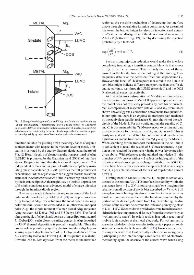
Fig. 12. Energy band diagram of a metal/Alq3 interface in the semi-insulating
(SI: top) and insulating (I: bottom) state (after Baldo and Forrest [31]). Electron
injectionto LUMOis promotedby theGaussiandensity of interfacestates(DOS)
in both cases, the I-state being the result of a damage to the true interface dipole
∆, caused possibly by injection of holes under positive biases on metal.
direction suitable for pushing down the energy bands of organicsemiconductor with respect to the vacuum level of metal, a sit-
uation illustrated by the energy diagram depicted at the top of
Fig. 12. Here, injection of electrons to the transport band of Alq3
(LUMO) is promoted by the Gaussian band (DOS) of interface
states. Keeping in mind that the fractional capacitance aC is
independent of bias and in parallel with the completely insu-
lating phase capacitance (1−a)C provides the full geometrical
capacitance C of the organic layer, we suggest that the resistor R
stands for the contact resistance of the interface region occupied
by the interfacedipole. A thorough study on the bias dependence
of R might contribute to an advanced model of charge injection
through the interface dipole region.
Now we are ready to handle this region in terms of the localorder model developed by Baldo et al. [29] and applied success-
fully to doped Alq3. For achieving the local order a strongly
polar material should be embedded in an otherwise undoped
polar Alq3, the dipole moment of a meridional Alq3 molecule
lying between 4.1 Debye [30] and 5.3 Debye [29]. The facial
phase molecule of Alq3 shouldpossess a largerdipole momentof
7.1 Debye [30], yet its close-to-surface content in Alq3 deposited
by UHV thermal deposition is probably negligible. Then the
crucial role is possibly played by the true interface dipole pos-
sessing a giant dipole moment of 30 Debye as deduced from
I –V curves by Baldo and Forrest [31]. If this picture is realistic,
it would lead to hole injection from the metal to the interface
region as the possible mechanism of destroying the interface
dipole through neutralizing its anion constituent. As a result of
this event the barrier height for electron injection (and extrac-
tion?) at the metal/Alq3 side of the device would increase by
∆≈1 eV (bottom of Fig. 12), thereby decreasing the injection
probability by a factor of
exp
∆
kT
≈ 6× 10¹⁶. (4)
Such a strong injection reduction would make the interface
completely insulating, a transition compatible with that shown
in Fig. 3 for the dc current. This is likely the case of the ac
current in the I-state, too, when looking at the missing low-
frequency data or at the persistent fractional capacitance C s.
However, the lone 103 Hz data point measured in the I-state at
zero bias might indicate different transport mechanisms for dc
and ac currents, e.g. through LUMO (extended) and the DOS
(via hopping) states, respectively.
At first sight any confrontation of I –V data with impedanceones expressed in terms of Model II appears impossible, since
the model does not explicitly provide any path for dc current.
Yet, a comparison of respective data on R and Rdc from tables
shown above suggests a correlation between the two quantities.
In our opinion, there is an implicit dc-transport path mediated
by the equivalent parallel resistance Rp (not shown) of the sub-
circuit of the Model I. For this configuration, the equality of C pand C s is documented (Fig. 7). Moreover, our experimental data
provide evidence for the equality of Rp and Rs as well. This is
easily understood if we define for both serial and parallel con-
figurations a unique time constant τ = RpC p = RsC s for Model I.
When searching for the transport mechanism in the dc limit, itis convenient to recall the results of I –V measurements, in par-
ticular the values of the exponent n in the power-law expression
given above. With reference to the standard knowledge [1], the
branches of I –V curves with n≈ 2 reflect the high-quality of the
organic material carrying space-charge limited currents (SCLC).
There have been a few cases when n approached values larger
than 3, a possible indication of the case of trap-limited current
flow [1].
Turning back to Model II, the R2, C 2 couple is tentatively
located at the bottom Alq3 /ITO interface. Its stability within the
bias range from −2 to 2 V is not surprising if one imagines the
relatively small portion of the dc bias absorbed by R2 R. Still
an explanation of having this almost ohmic back contact remainsa riddle. It remains to go back to the I-state represented by the
portion of the dashed j–U curve from Fig. 3 exhibiting the dis-
persion of the residual dc current, the inflexion point lying close
to U =−1.5 V. We consider the residual current to include a con-
siderable ionic component well known from electrochemistry as
“voltammetric wave”. Its origin resides in a redox reaction of
mobile ionic species at the metal electrode. For voltammetric
waves in solid electrolytes we refer to the review paper on solid-
state voltammetry by Kulesza and Cox [33]. In our case, we tend
to assign the wave to at least partially mobile cations (originally
participating in the interface dipole) reduced at the Al electrode,
mentioning again the absence of the current wave when using

7/29/2019 Inhomogeneous Transport of Alq3
http://slidepdf.com/reader/full/inhomogeneous-transport-of-alq3 9/10
1116 I. Thurzo et al. / Synthetic Metals 156 (2006) 1108–1117
Ag electrodes on top. One cannot exclude ionic species from the
surrounding atmosphere from playing a role in this slow charge
relaxation. This may be the right moment to touch the kinetics
of the equilibration of in situ Alq3 with atmosphere. The semi-
conducting or semiinsulating states stabilize on a time scale of
minutes after taking out devices from UHV. The bias-induced
I-state can be maintained for days, at least when the bias does
not exceed the interval used during the experiments presented.
Once the I-state has been reached, it is impossible to restore the
(non-ohmic) S- or SI-state without destroying the device.
A confrontation of present results with directly related pub-
lished work [27,28] deserves attention. Even though related
steady-state I –V curves of either PPV- or Alq3-based devices
were not shown in the publications, the polarity of bias may
correspond to the forward direction in each case. The data corre-
spond rather to admittance measurements (R−1p , C p) at different
frequencies and biases and exhibit pronounced dependence of
both components on frequency at a given bias. Despite quite dif-
ferent organic materials the published zero-bias data exhibit a
common distinct feature not compatible with our present results:the relative permittivities εr, as deduced from the overall high-
frequency capacitances, correspond to 2 (PPV) and 4 (Alq3),
respectively, while always showing a continuous increase when
lowering the frequency. The zero-bias conductanceG(ω) = R−1p
reported by Berleb andBrutting [27] f or E ≈105 V cm−1 may be
viewed as signaling the I-state. Under applied bias an apparent
negative contribution to capacitance is reported and assigned to
the relaxation of the injected space charge [27,28]. When pass-
ing to low frequencies, there is an apparent minimum (due to the
negative component) followed by a steep increase of the capaci-
tance, the minimum resulting from the interference between the
possibly negative component and the increasing dielectric lossdue to dc current. Berleb and Brutting [27] accepted the ear-
lier suggested analysis of the negative component [28] in terms
of a distribution of times-of-flight of injected excess carriers,
classifying the steep increase of capacitance as an indication
of dispersive transport, to be characterized by the dispersion
parameter ␣. Our results corresponding to even lower electric
fields are contradictory in the sense that one deals with an instru-
mental artifact due to excess conduction loss of whatever origin.
Moreover, our results and analysis presented above can be dealt
with an equivalent circuit composed of frequency independent
elements and εr≈ 2, the latter permittivity being in accordance
with the results on PPV by Martens et al. [28]. Nonetheless, even
some of their low-frequency admittance data are suspected of becoming inaccurate due to dc leakage of the diodes.
5. Conclusions
Evidence is provided for lateral inhomogeneity in the mor-
phology of Alq3 manifesting itself as a phase separation
deduced from the current–voltage and impedance behavior of
metal/Alq3 /ITO devices prepared in situ by thermal evapo-
ration and measured in air. Two phases seem to coexist in
the Alq3 thin films: an (instrumentally) completely insulating
(amorphous) phase along with a more or less conducting phase
building an interface dipole with the top metal (Ag, Al) elec-
trode. Such a coexistence is revealed by modeling the experi-
mentally observed fractional geometrical capacitance (1− a)C
(a = 0.5–0.7) of the devices as one component of the equiva-
lent circuit composed of frequency independent elements. The
interface dipole zone is represented by a bias-dependent contact
resistance in series with the complementary geometrical capac-
itance aC of the insulating bulk of Alq3. There seems to be a
correlation between this ac contact resistance and the dc resis-
tance as determined from I –V measurements. The dc current
obeys a power-law dependence ∝ U n on bias U , the coeffi-
cient n covering the range from 2 to 3.5 (space-charge to trap-
limited currents). The local formation of the zone is interpreted
within the framework of the metal/Alq3 energy band diagram
developed by Baldo and Forrest [31], along with the model of
dipole–dipole interaction leading to a local order (Baldo et al.
[29]). It is suggested that the local order is due to an interac-
tion of the giant interface dipole (30 Debye) with the intrinsic
dipoles of Alq3 molecules. The semiconducting phase under-
goes an irreversible semiinsulator-to-insulator transition undera critical positive potential of the top metal electrode. This tran-
sition is tentatively interpreted as coming from hole injection
and subsequent neutralization of the anion of the giant interface
dipole, thereby destroying the latter. The Alq3 /ITO barrier lead-
ing to an observable dispersion of the real part of impedance
at high frequencies is modeled via a linear parallel RC circuit
independent of the related absorbed portion of applied dc bias.
High-sensitivity impedance instrumentationis needed to acquire
low-frequency data on insulating Alq3, thereby enabling a com-
parison of transport mechanisms in frequency- and time-domain
(dc limit).
References
[1] W. Brutting, S. Berleb, A.G. Muckl, Org. Electron. 2 (2001) 1.
[2] J.C. Scott, J. Vac. Sci. Technol. A 21 (2003) 521.
[3] P.E. Burrows, Z. Shen, V. Bulovic, D.M. McCarty, S.R. Forrest, J. Appl.
Phys. 79 (1996) 7991.
[4] A. Curioni, M. Boero, W. Androni, Chem. Phys. Lett. 294 (1998) 263.
[5] M. Colle, R.E. Dinnebier, W. Brutting, Chem. Commun. (2002) 2908.
[6] M. Colle, S. Forero-Lenger, J. Gmeiner, W. Brutting, Phys. Chem. Chem.
Phys. 5 (2003) 2958.
[7] M. Colle, J. Gmeiner, W. Milius, H. Hillebrecht, W. Brutting, Adv. Funct.
Mater. 13 (2003) 108.
[8] M. Colle, W. Brutting, Phys. Status Solidi (a) 201 (2004) 1095.
[9] R.L. Martin, J.D. Kress, I.H. Cmpbell, D.L. Smith, Phys. Rev. B 61 (2000)15804.
[10] H. Aziz, Z.D. Popovic, N.-X. Hu, A.-M. Hor, G. Xu, Science 283 (1999)
1900.
[11] D.Y. Kondakov, J.R. Sandifer, C.W. Tang, R.H. Young, J. Appl. Phys. 93
(2003) 1108.
[12] D.Y. Kondakov, J. Appl. Phys. 97 (2005), 024503.
[13] F. Papadimitrakopoulos, X.-M. Zhang, Synth. Met. 85 (1997) 1221.
[14] S.H. Kim, H.Y. Chu, T. Zyung, Y.S. Yang, ETRI J. 26 (2004) 161.
[15] M.S. Xu, J.B. Xu, Thin Solid Films 491 (2005) 317.
[16] L.F. Cheng, L.S. Liao, W.Y. Lai, X.H. Sun, N.B. Wong, C.S. Lee, S.T. Lee,
Chem. Phys. Lett. 319 (2000).
[17] H. Mu, H. Shen, D. Klotzkin, Solid State Electron. 48 (2004) 2085.
[18] C.B. Lee, A. Uddin, X. Hu, T.G. Andersson, Mater. Sci. Eng. B 112 (2004)
14.
[19] I.H. Campbell, D.L. Smith, J.P. Ferraris, Appl. Phys. Lett. 66 (1995) 3030.

7/29/2019 Inhomogeneous Transport of Alq3
http://slidepdf.com/reader/full/inhomogeneous-transport-of-alq3 10/10
I. Thurzo et al. / Synthetic Metals 156 (2006) 1108–1117 1117
[20] Y. Li, J. Gao, G. Yu, Y. Cao, A.J. Heeger, Chem. Phys. Lett. 287 (1998) 83.
[21] G. Yu, Y. Cao, Ch. Zhang, Y. Li, J. Gao, A.J. Heeger, Appl. Phys. Lett. 73
(1998) 111.
[22] W. Brutting, H. Riel, T. Beierlein, W. Riess, J. Appl. Phys. 89 (2001) 1704.
[23] G. Paasch, S. Scheinert, Synth. Met. 122 (2001) 145.
[24] G.L. Pakhomov, V.I. Shashkin, D.E. Pozdnyaev, C. Muller, J.-M. Ribo,
Org. Electron. 3 (2002) 93.
[25] Y.S. Yeong, D. Troadec,A. Moliton,B. Ratier, R. Antony, G. Veriot, Synth.
Met. 127 (2002) 195.[26] P. Stallinga, H.L. Gomes, M. Murgia, K. Mullen, Org. Electron. 3 (2002)
43.
[27] S. Berleb, W. Brutting, Phys. Rev. Lett. 89 (2002) 286601.
[28] H.C.F. Martens, H.B. Brom, P.W.M. Blom, Phys. Rev. B 60 (1999)
R8489.
[29] M.A. Baldo, Z.G. Soos, S.R. Forrest, Chem. Phys. Lett. 347 (2001)
297.
[30] H. Ishii, N. Hayashi, E. Ito, Y. Washizu, K. Sugi, Y. Kimura, M. Nivano,
Y. Ouchi, K. Seki, Phys. Status Solidi (a) 201 (2004) 1075.
[31] M.A. Baldo, S.R. Forrest, Phys. Rev. B 64 (2001) 085201.
[32] S.A. Van Slyke, C.H. Chen, C.W. Tang, Appl. Phys. Lett. 69 (1996)2160.
[33] P.J. Kulesza, J.A. Cox, Electroanalysis 10 (1998) 73.