inhomogeneity of the ultrafast insulator-to-metal...
TRANSCRIPT
ARTICLE
Received 24 Aug 2014 | Accepted 5 Mar 2015 | Published 21 Apr 2015
Inhomogeneity of the ultrafast insulator-to-metaltransition dynamics of VO2
Brian T. O’Callahan1, Andrew C. Jones1, Jae Hyung Park2, David H. Cobden2, Joanna M. Atkin1,3
& Markus B. Raschke1
The insulator-metal transition (IMT) of vanadium dioxide (VO2) has remained a long-
standing challenge in correlated electron physics since its discovery five decades ago. Most
interpretations of experimental observations have implicitly assumed a homogeneous
material response. Here we reveal inhomogeneous behaviour of even individual VO2
microcrystals using pump-probe microscopy and nanoimaging. The timescales of the ultrafast
IMT vary from 40±8 fs, that is, shorter than a suggested phonon bottleneck, to 200±20 fs,
uncorrelated with crystal size, transition temperature and initial insulating structural phase,
with average value similar to results from polycrystalline thin-film studies. In combination
with the observed sensitive variations in the thermal nanodomain IMT behaviour, this sug-
gests that the IMT is highly susceptible to local changes in, for example, doping, defects and
strain. Our results suggest an electronic mechanism dominating the photoinduced IMT, but
also highlight the difficulty to deduce microscopic mechanisms when the true intrinsic
material response is yet unclear.
DOI: 10.1038/ncomms7849
1 Department of Physics, Department of Chemistry, and JILA, University of Colorado, Boulder, Colorado, 80309, USA. 2 Department of Physics, University ofWashington, Seattle, Washington 98195, USA. 3 Department of Chemistry, University of North Carolina, Chapel Hill, North Carolina 27599, USA.Correspondence and requests for materials should be addressed to J.M.A. (email: [email protected]) or to M.B.R. (email: [email protected]).
NATURE COMMUNICATIONS | 6:6849 | DOI: 10.1038/ncomms7849 | www.nature.com/naturecommunications 1
& 2015 Macmillan Publishers Limited. All rights reserved.

Vanadium dioxide (VO2) is one of the prototypicalcorrelated-electron materials, exhibiting an insulator-metal transition (IMT), with a change in resistivity of
several orders of magnitude that can be induced thermally atTB340 K (refs 1,2), or optically3. The photoinduced IMT occurson subpicosecond timescales, and therefore has a non-thermalbasis. This ultrafast transition has been studied using a widevariety of spectroscopies, with short-pulse optical3–6, terahertz7–9,X-ray10–12 and electron diffraction13–15 techniques. These studieshave addressed the ultrafast electron dynamics and latticestructural processes that occur during the transition, in additionto slower behaviour over multi-picosecond to nanosecondtimescales. However, the mechanism underlying both thethermal and photoinduced IMT remains unclear. Whileinsulating VO2 is clearly not a band insulator16, the importanceof electron correlations and electron–phonon coupling for itsproperties remain unclear after more than half a century of study,and experimental results conflict with both Mott or Peierlsexplanations7,16–19. For example, degenerate pump-probestudies5 revealed a limiting transition timescale of 75 fs,suggesting a phonon bottleneck and therefore a structurallylimited transition. In contrast, the observation of coherentphonon oscillations above the apparent threshold for triggeringthe photoinduced phase transition7 indicates that thephotoinduced IMT is decoupled from the structural transition.
Much of the work on VO2 has focused on polycrystalline thinfilms, grown by a variety of techniques20. Recently, differencesobserved in the ultrafast and thermal properties due to anisotropyand grain size in polycrystalline and epitaxial thin filmsamples9,21–23 suggest that growth conditions can substantiallymodify the measured response. These results contributed to theconfusion in the interpretation of previous measurements.Furthermore, most spectroscopy techniques average overmultiple crystallites, subject to large inhomogeneous strain,which could, for example, create mixtures of different competingphases. While nanoimaging techniques such as scattering scanningnear-field optical microscopy (s-SNOM)18 can access theheterogeneity in thin films, the complicating extrinsic inter-actions among crystallites make results difficult to interpret.
To overcome the limitations of averaging over ensembles ofcrystallites and other heterogeneities, we investigate individual
VO2 single microcrystals. We perform degenerate pump-probemicroscopy to monitor the femtosecond dynamics following theultrafast photoexcitation. In addition, we use infrared s-SNOM toprobe the nanoscopic details of the evolution of the spatial phasecompetition in the thermal IMT. These studies allow us toobserve the inhomogeneity in the dynamics among the micro-crystals measured, finding highly variable timescales associatedwith the photoinduced bandgap reorganization. In combinationwith micro-Raman spectroscopy, we systematically study therelationship of crystallographic orientation, insulating phaseand temperature to the photoinduced response dynamics. Withs-SNOM infrared nanoimaging, we monitor the growth andevolution of metallic and insulating domains through the thermaltransition with 10-nm spatial resolution, and find highlytemperature sensitive variations in the spatial organization ofthe domain structure in the individual single crystals. Theseresults suggest a unusually high sensitivity of both the photo-induced and thermal IMT of VO2 to yet unresolved smallperturbations in the form of defects or strain.
ResultsSingle-crystal pump-probe microscopy. A schematic of thedegenerate pump-probe experiment is shown in Fig. 1a, withdetails described in the Methods section. We perform frequency-resolved optical gating (FROG) of the laser pulses (Fig. 1b) anddetermine a pulse duration of B45 fs. We use the pulse char-acteristics (Fig. 1c) as parameters for the fit of the transientreflectivity (see Results section), to resolve 10 s of fs dynamics ofthe photoinduced transition by deconvolution.
The VO2 microcrystals that we study are grown by vapourtransport24. They show an abrupt, first-order transition in theabsence of strain or doping25, in contrast to the percolationbehaviour observed in thin-film samples18. The crystals vary insize (Fig. 1d), and are highly structurally homogeneous, with a flatsurface (root mean squared roughness o1.8 nm).
We characterize the crystallographic orientation, insulatingphase and thermal transition temperature using micro-Ramanspectroscopy and s-SNOM26 for all of the microcrystals measuredin these experiments. In the Raman spectra, the shift of the oV�O
Raman mode, at B600 cm� 1, allows us to estimate the amount
Delay �
PD
PolarizerSample
95:5 B.S.
Probe arm
Pump arm
Optical chopper
� = 800 nm� = 45 fsRep. rate = 125 kHz
Epu
lse
0
Pha
se (
rad)
Time (fs)0 50–50–100 1000 50–50–100
Time (fs)100
Wav
elen
gth
(nm
)
800
820
780
150
0 nm1 μm
25 μm
π
z
xy
�
Figure 1 | Single-crystal VO2 ultrafast pump-probe microscopy (a) Schematic of optical layout. (b) Typical FROG spectrogram of pulse, with (c) full phase
and amplitude reconstruction in time domain showing B45 fs pulse duration and small chirp. (d) Optical microscope image of VO2 microcrystals on Si/
SiO2 substrate. (e) Atomic force microscopy topography showing the homogeneous nature of the microcrystals.
ARTICLE NATURE COMMUNICATIONS | DOI: 10.1038/ncomms7849
2 NATURE COMMUNICATIONS | 6:6849 | DOI: 10.1038/ncomms7849 | www.nature.com/naturecommunications
& 2015 Macmillan Publishers Limited. All rights reserved.

of strain within the crystal due to substrate interactions ordoping. Three possible insulating structures can be distinguished,monoclinic 1 (M1), intermediate triclinic (T) and monoclinic 2(M2), with increasing degrees of strain27 (Fig. 2a). With theirwell-defined, controllable strain state and ability to withstand ahigh degree of strain, microcrystal samples have been studied toinvestigate the strain–temperature phase diagrams for VO2 (seeFig. 2b)27–31. The very low-luminescence background and narrowlinewidths in Raman spectroscopy indicate a low defect densityand confirm a high structural quality of the VO2 microcrystals.
For low pump fluences, the transient reflectivity responseshows an initial electronic excitation, due to the above-gapexcitation of the pump, followed by relaxation on a picosecondtimescale, as seen in Fig. 2c. Probing at 800 nm (1.55 eV), theresponse is expected to be dominated by electrons in the d|| bandsclose to the Fermi level6,32,33. The modulations in the reflectivitysignal indicate the excitation of coherent phonons in theinsulating phase34.
An orientational anisotropy is evident in the relaxation andcoherent phonon behaviour, with faster decay and moreprominent oscillations for probe polarization perpendicular(pump parallel) to the crystallographic cR-axis (black line),compared with probe parallel (pump perpendicular; red line).The Fourier transform phonon spectrum, shown in Fig. 2d,reveals an even more pronounced anisotropy. For probepolarization perpendicular to the cR axis, only one low energyphonon peak is resolved, at B200 cm� 1 (6 THz). For parallel
probe polarization, both phonon modes emerge, with the secondat B225 cm� 1 (6.7 THz). The reflectivity change at 3 ps alsoshows an angular anisotropy, with a cos2y dependence with angley of probe polarization with respect to the cR axis (Fig. 2e).
At higher fluences, the coherent phonon response is dimin-ished, eventually vanishing for fluences sufficiently high to drivethe microcrystal through the photoinduced IMT (Fig. 3a). Thepersistence of the reflectivity change (up to microseconds)indicates a metastable metal-like state. However, without asimultaneous structural probe, we cannot determine the crystal-lographic structure during this period and whether this statecorresponds to a rutile or monoclinic metallic state19,35,36. Theinset shows the reflectivity �DR/R at 1 ps plotted as a function offluence, to derive the threshold fluence Fth. Fth for differentmicrocrystals varies between 2 and 6 mJ cm� 2, which weattribute to variable coupling to the substrate. These values areclose to or slightly lower than those observed in thin films, whichrange from B5.5 mJ cm� 2 up to 415 mJ cm� 2 (refs 6,11,36,37),due to stronger substrate coupling.
To quantify the transition dynamics and relate to thephysical characteristics of the different microcrystals, wefit the above-threshold transient reflectivity behaviour to�DR=RðtÞ ¼ IðtÞ � f ðtÞ. Here f(t), the response function ofthe microcrystal, is convolved with I(t), the transient intensity ofthe pulse from FROG analysis, which accounts for the timeresolution and the step-like excitation at t¼ 0 without a prioriassumptions about pulse duration or shape (see Methods section
Ten
sile
str
ain
M1
M2
T
0
1
2
3
4
5
Inte
nsity
(ar
b. u
.)
200 300 400 500 600 700Raman shift (cm–1)
Perpendicular
Parallel
6 �V-O
–ΔR
/R
6543210Pump-probe delay � (ps)
0
45
90
135
180
225
270
315
–ΔR/R(�) for � = 3 ps
CR
CR10–4
10–5
10–3
Temp.
T
M1
M2
Wavenumber (cm–1)
CP
spe
c. (
arb.
u.)
180 200 220 240
0
1
2
3
4
�
�V2�V1
�V2
�V1
R0
338 K
Figure 2 | Insulating microcrystal phase characterization (a) Raman spectra of the three insulating phases, M1 (green, crystal #1), M2 (dark blue, crystal
#20) and intermediate triclinic T (light blue, crystal #4). Perpendicular (black) and parallel (red) Raman polarization with respect to cR of a microcrystal in
the M1 phase. (b) Strain–temperature phase diagram showing relation of three insulating phases to metallic rutile phase (gray)27,28. (c) Transient
reflectivity traces of crystal #29, �DR/R, for low fluence with coherent phonon excitation, with probe polarization parallel (red) and perpendicular (black)
to the cR axis. The pump pulse is shown in red near time zero. Inset: corresponding image of a microcrystal illustrating the probe polarization geometry.
Scale bar, 5 mm. (d) Fourier transform spectra of the reflectivity traces, exhibiting phonon modes at B200 and B220 cm� 1. (e) Reflectivity at 3 ps for
different probe polarizations (pump perpendicular to probe).
NATURE COMMUNICATIONS | DOI: 10.1038/ncomms7849 ARTICLE
NATURE COMMUNICATIONS | 6:6849 | DOI: 10.1038/ncomms7849 | www.nature.com/naturecommunications 3
& 2015 Macmillan Publishers Limited. All rights reserved.

for more details on the convolution procedure). f(t) is modelled asa biexponential function:
f ðtÞ ¼ � R11þ a
e� t=tf þ ae� t=ts
� �þR1; ð1Þ
with tf the initial, ultrashort transition time, constrained too1 ps. ts captures the longer timescale behaviour, with2 psotso10 ps, RN describes the magnitude of the reflectivitychange and the parameter a sets the relative scaling of the fast andslow exponential terms. We find that the contribution from slowdynamics is generally small (that is, aoo1) and therefore wefocus here on the short timescale dynamics captured by tf.
Representative fits of the transient reflectivity response forcrystal #13 for a range of above-threshold fluences are shown inFig. 3b (black dashed lines), with �DR/R normalized for clarity.For the o500-fs range, the response is dominated by tf. Weobserve three distinct characteristics in the ultrafast initialresponse. First, for the lowest fluence investigated we see atransition time of tf¼ 40±8 fs, shorter than the previouslyobserved dynamics in any VO2 sample, as discussed furtherbelow. Second, we observe a dramatic, up to threefold increase intransition time with increasing fluence (b, inset), in contrast to adecrease observed in previous work on polycrystalline films3,6.Third, we see the transition time tf decrease with increasingsample temperature (Fig. 3c). During the measurement, we usedsufficiently low laser repetition rates (o100 kHz) to allowcomplete relaxation to the initial insulating state, thusminimizing the effects due to hysteresis that can occur close tothe transition temperature. Through the combination withRaman spectroscopy, we can correlate this temperature-dependent change with the structural changes of the insulatingphase on heating, as has been observed previously27. The pump-probe measurement at T¼ 352 K has a small change in transientreflectivity and large uncertainty, since at this temperaturemetallic domains have appeared due to thermal excitation.
The data shown in Fig. 3 are for two different microcrystals.Figure. 3a,c shows fluence and temperature dependence for
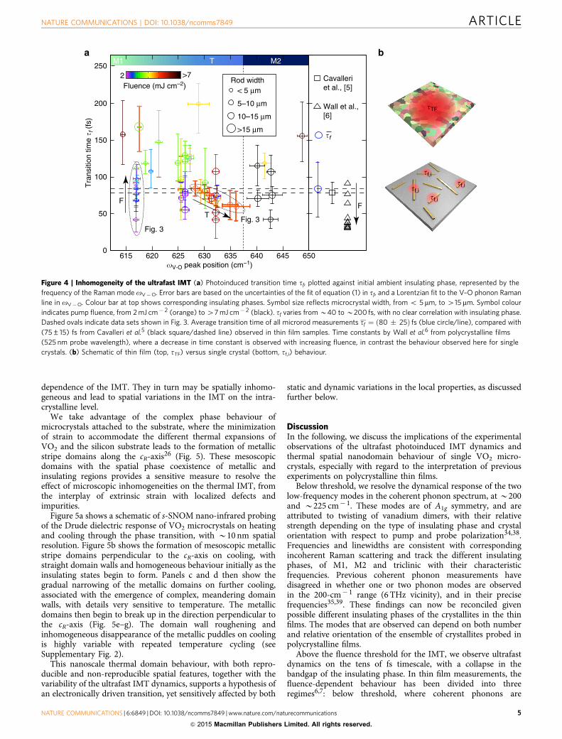
crystal #30 (see Supplementary Fig. 1 and Supplementary Note 1for discussion of hysteresis effects during the thermal MITtransition) and Fig. 3b shows data for crystal #13, respectively.The trends of an increase in tf with increasing fluence and adecrease in tf with increasing temperature are seen for allmeasured microcrystals, though extracted transition times varybetween crystals. The transition times tf obtained from allmeasurements on 28 microcrystals of different sizes, and forselected different initial temperatures, and range of fluences aresummarized in Fig. 4 and Supplementary Table 1. The values areshown as a function of the measured oV�O phonon frequencyfrom Raman spectroscopy, as a proxy for the different insulatingphases of the crystals (indicated by green–blue colour bar for theM1, T and M2 phases). The error bars are based on the statisticaluncertainties of the fit of equation (1) in tf, and a Lorentzian fit tothe V–O phonon Raman line in oV�O. Different microcrystalwidths are indicated by the size of the data symbols (see legend),from o5 mm to 415mm. The fluences used are all above thethreshold fluence for the specific microcrystal, with valuesindicated using false colour. The values of tf vary reproduciblyfrom 40 to 200 fs for each crystallite. Notably, the averagevalue of tf over all microcrystals is found to be tf ¼ 80 � 25 withtf� 1 ¼
Pi t� 1f ;i (blue circle). This value is in striking agreement
with transition times tTF from thin-film studies5 (Fig. 4b).
s-SNOM imaging. The large variations in tf indicate that thephotoinduced IMT is highly sensitive with respect to unknownelectronic or structural heterogeneities between different crystal-lites. This inhomogeneity appears to be uncorrelated with struc-ture, strain, temperature or microcrystal size, with no consistentbehaviour even between crystals attached to the substrate (that is,strained) or free. This suggests a high susceptibility of tf to minorvariations in doping, stoichiometric details or defects. Thesevariations are small enough that they are not reflected in thelattice structure at the level detectable by few-wavenumberRaman shifts, nor in the macroscopic strain or temperature
0 500 1,000 1,500
10−4
10−3
10−2
Pump-probe delay � (fs)
–ΔR
/R 0 100 200 300 400 500
2
3
45678
10
Delay � (fs)
–ΔR
/R (
norm
aliz
ed)
300 320 340 3600
20
40
60
80
100
Tra
nsiti
on ti
me
� f (
fs)
625
630
635
640
645
650
Temperature (K)
�V
-O p
eak
posi
tion
(cm
–1)
2.0 2.4 2.8 3.2
40
80
120
Fluence (mJ cm–2)
� f (
fs)
2 3 4 5 6 70
1
2
Fluence (mJ cm–2)
–ΔR
/R (
×10–4
)
Thresholdfluence
–ΔR/R at 1 ps
1.6
2.1
3.43.2
4.04.3 mJ cm–2
Incr.fluence
Figure 3 | Fluence and temperature dependence (a) Fluence-dependent transient reflectivity traces �DR/R for crystal #30. Inset shows the non-linear
dependence of the reflectivity with fluence at t¼ þ 1 ps delay. (b) Change in short timescale dynamics with fluence for F4Fth, on crystal #13. Black lines
show fits to exponential recovery behaviour, with extracted transition time tf shown in the inset. (c) Variation of transition time with temperature, measured
at 3.3 mJ cm� 2, showing a decrease in tf with increasing temperature (crystal #30). This is correlated with a change in insulating structure, as monitored
through the oV�O Raman mode (see Supplementary Table 2). Error bars are based on the uncertainties of the fit of equation (1) in tf, and a Lorentzian fit to
the V–O phonon Raman line in oV�O. Blue and red dashed lines are guides to the eye.
ARTICLE NATURE COMMUNICATIONS | DOI: 10.1038/ncomms7849
4 NATURE COMMUNICATIONS | 6:6849 | DOI: 10.1038/ncomms7849 | www.nature.com/naturecommunications
& 2015 Macmillan Publishers Limited. All rights reserved.
dependence of the IMT. They in turn may be spatially inhomo-geneous and lead to spatial variations in the IMT on the intra-crystalline level.
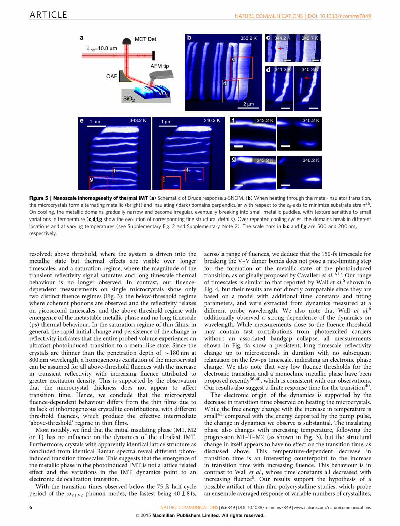
We take advantage of the complex phase behaviour ofmicrocrystals attached to the substrate, where the minimizationof strain to accommodate the different thermal expansions ofVO2 and the silicon substrate leads to the formation of metallicstripe domains along the cR-axis26 (Fig. 5). These mesoscopicdomains with the spatial phase coexistence of metallic andinsulating regions provides a sensitive measure to resolve theeffect of microscopic inhomogeneities on the thermal IMT, fromthe interplay of extrinsic strain with localized defects andimpurities.
Figure 5a shows a schematic of s-SNOM nano-infrared probingof the Drude dielectric response of VO2 microcrystals on heatingand cooling through the phase transition, with B10 nm spatialresolution. Figure 5b shows the formation of mesoscopic metallicstripe domains perpendicular to the cR-axis on cooling, withstraight domain walls and homogeneous behaviour initially as theinsulating states begin to form. Panels c and d then show thegradual narrowing of the metallic domains on further cooling,associated with the emergence of complex, meandering domainwalls, with details very sensitive to temperature. The metallicdomains then begin to break up in the direction perpendicular tothe cR-axis (Fig. 5e–g). The domain wall roughening andinhomogeneous disappearance of the metallic puddles on coolingis highly variable with repeated temperature cycling (seeSupplementary Fig. 2).
This nanoscale thermal domain behaviour, with both repro-ducible and non-reproducible spatial features, together with thevariability of the ultrafast IMT dynamics, supports a hypothesis ofan electronically driven transition, yet sensitively affected by both
static and dynamic variations in the local properties, as discussedfurther below.
DiscussionIn the following, we discuss the implications of the experimentalobservations of the ultrafast photoinduced IMT dynamics andthermal spatial nanodomain behaviour of single VO2 micro-crystals, especially with regard to the interpretation of previousexperiments on polycrystalline thin films.
Below threshold, we resolve the dynamical response of the twolow-frequency modes in the coherent phonon spectrum, at B200and B225 cm� 1. These modes are of A1g symmetry, and areattributed to twisting of vanadium dimers, with their relativestrength depending on the type of insulating phase and crystalorientation with respect to pump and probe polarization34,38.Frequencies and linewidths are consistent with correspondingincoherent Raman scattering and track the different insulatingphases, of M1, M2 and triclinic with their characteristicfrequencies. Previous coherent phonon measurements havedisagreed in whether one or two phonon modes are observedin the 200-cm� 1 range (6 THz vicinity), and in their precisefrequencies35,39. These findings can now be reconciled givenpossible different insulating phases of the crystallites in the thinfilms. The modes that are observed can depend on both numberand relative orientation of the ensemble of crystallites probed inpolycrystalline films.
Above the fluence threshold for the IMT, we observe ultrafastdynamics on the tens of fs timescale, with a collapse in thebandgap of the insulating phase. In thin film measurements, thefluence-dependent behaviour has been divided into threeregimes6,7: below threshold, where coherent phonons are
M1 T
615 620 625 630 635 640 645 6500
50
100
150
200
250
�V-O peak position (cm−1)
Tra
nsiti
on ti
me
� f (
fs)
Fluence (mJ cm–2)2
Fig. 3
�TF
�f,i
�f,i
�f,i
�f,i
ba
Wall et al.,[6]
Cavalleriet al., [5]
�f
>7
F
TF
M2
>15 μm
< 5 μm
5–10 μm
10–15 μm
Rod width
Fig. 3
Figure 4 | Inhomogeneity of the ultrafast IMT (a) Photoinduced transition time tf, plotted against initial ambient insulating phase, represented by the
frequency of the Raman mode oV�O. Error bars are based on the uncertainties of the fit of equation (1) in tf, and a Lorentzian fit to the V–O phonon Raman
line in oV�O. Colour bar at top shows corresponding insulating phases. Symbol size reflects microcrystal width, from o 5 mm, to 415 mm. Symbol colour
indicates pump fluence, from 2 mJ cm� 2 (orange) to 47 mJ cm� 2 (black). tf varies from B40 to B200 fs, with no clear correlation with insulating phase.
Dashed ovals indicate data sets shown in Fig. 3. Average transition time of all microrod measurements tf ¼ ð80 � 25Þ fs (blue circle/line), compared with
(75±15) fs from Cavalleri et al.5 (black square/dashed line) observed in thin film samples. Time constants by Wall et al.6 from polycrystalline films
(525 nm probe wavelength), where a decrease in time constant is observed with increasing fluence, in contrast the behaviour observed here for single
crystals. (b) Schematic of thin film (top, tTF) versus single crystal (bottom, tf,i) behaviour.
NATURE COMMUNICATIONS | DOI: 10.1038/ncomms7849 ARTICLE
NATURE COMMUNICATIONS | 6:6849 | DOI: 10.1038/ncomms7849 | www.nature.com/naturecommunications 5
& 2015 Macmillan Publishers Limited. All rights reserved.
resolved; above threshold, where the system is driven into themetallic state but thermal effects are visible over longertimescales; and a saturation regime, where the magnitude of thetransient reflectivity signal saturates and long timescale thermalbehaviour is no longer observed. In contrast, our fluence-dependent measurements on single microcrystals show onlytwo distinct fluence regimes (Fig. 3): the below-threshold regimewhere coherent phonons are observed and the reflectivity relaxeson picosecond timescales, and the above-threshold regime withemergence of the metastable metallic phase and no long timescale(ps) thermal behaviour. In the saturation regime of thin films, ingeneral, the rapid initial change and persistence of the change inreflectivity indicates that the entire probed volume experiences anultrafast photoinduced transition to a metal-like state. Since thecrystals are thinner than the penetration depth of B180 nm at800 nm wavelength, a homogeneous excitation of the microcrystalcan be assumed for all above-threshold fluences with the increasein transient reflectivity with increasing fluence attributed togreater excitation density. This is supported by the observationthat the microcrystal thickness does not appear to affecttransition time. Hence, we conclude that the microcrystalfluence-dependent behaviour differs from the thin films due toits lack of inhomogeneous crystallite contributions, with differentthreshold fluences, which produce the effective intermediate‘above-threshold’ regime in thin films.
Most notably, we find that the initial insulating phase (M1, M2or T) has no influence on the dynamics of the ultrafast IMT.Furthermore, crystals with apparently identical lattice structure asconcluded from identical Raman spectra reveal different photo-induced transition timescales. This suggests that the emergence ofthe metallic phase in the photoinduced IMT is not a lattice relatedeffect and the variations in the IMT dynamics point to anelectronic delocalization transition.
With the transition times observed below the 75-fs half-cycleperiod of the oV1,V2 phonon modes, the fastest being 40±8 fs,
across a range of fluences, we deduce that the 150-fs timescale forbreaking the V–V dimer bonds does not pose a rate-limiting stepfor the formation of the metallic state of the photoinducedtransition, as originally proposed by Cavalleri et al.5,15. Our rangeof timescales is similar to that reported by Wall et al.6 shown inFig. 4, but their results are not directly comparable since they arebased on a model with additional time constants and fittingparameters, and were extracted from dynamics measured at adifferent probe wavelength. We also note that Wall et al.6
additionally observed a strong dependence of the dynamics onwavelength. While measurements close to the fluence thresholdmay contain fast contributions from photoexcited carrierswithout an associated bandgap collapse, all measurementsshown in Fig. 4a show a persistent, long timescale reflectivitychange up to microseconds in duration with no subsequentrelaxation on the few-ps timescale, indicating an electronic phasechange. We also note that very low fluence thresholds for theelectronic transition and a monoclinic metallic phase have beenproposed recently36,40, which is consistent with our observations.Our results also suggest a finite response time for the transition40.
The electronic origin of the dynamics is supported by thedecrease in transition time observed on heating the microcrystals.While the free energy change with the increase in temperature issmall41 compared with the energy deposited by the pump pulse,the change in dynamics we observe is substantial. The insulatingphase also changes with increasing temperature, following theprogression M1–T–M2 (as shown in Fig. 3), but the structuralchange in itself appears to have no effect on the transition time, asdiscussed above. This temperature-dependent decrease intransition time is an interesting counterpoint to the increasein transition time with increasing fluence. This behaviour is incontrast to Wall et al., whose time constants all decreased withincreasing fluence6. Our results support the hypothesis of apossible artifact of thin-film polycrystalline studies, which probean ensemble averaged response of variable numbers of crystallites,
340.3 K
343.7 K
2 μm
343.2 K
MCT Det.
VO2
�inc=10.8 μm
OAP
AFM tip
SiO2
344.2 K
341.2 K
353.2 K
1 μm 1 μm 340.2 K 343.2 K
343.2 K
340.2 K
340.2 K
c
d
fg g
f
Figure 5 | Nanoscale inhomogeneity of thermal IMT (a) Schematic of Drude response s-SNOM. (b) When heating through the metal-insulator transition,
the microcrystals form alternating metallic (bright) and insulating (dark) domains perpendicular with respect to the cR-axis to minimize substrate strain26.
On cooling, the metallic domains gradually narrow and become irregular, eventually breaking into small metallic puddles, with texture sensitive to small
variations in temperature (c,d,f,g show the evolution of corresponding fine structural details). Over repeated cooling cycles, the domains break in different
locations and at varying temperatures (see Supplementary Fig. 2 and Supplementary Note 2). The scale bars in b,c and f,g are 500 and 200 nm,
respectively.
ARTICLE NATURE COMMUNICATIONS | DOI: 10.1038/ncomms7849
6 NATURE COMMUNICATIONS | 6:6849 | DOI: 10.1038/ncomms7849 | www.nature.com/naturecommunications
& 2015 Macmillan Publishers Limited. All rights reserved.
each with varying transition times and threshold fluences. Theensemble measurement will therefore appear to be asuperposition of multiple timescales, requiring a larger numberof fitting parameters and producing different fluence-dependentbehaviour.
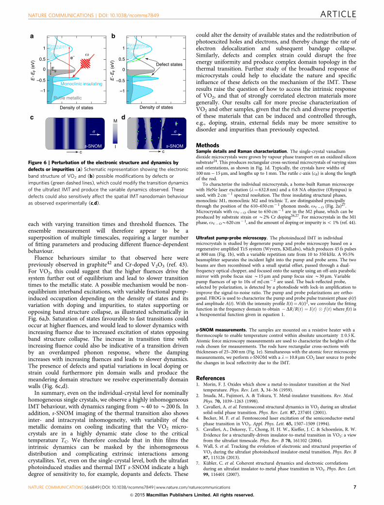
Fluence behaviours similar to that observed here werepreviously observed in graphite42 and Cr-doped V2O3 (ref. 43).For VO2, this could suggest that the higher fluences drive thesystem further out of equilibrium and lead to slower transitiontimes to the metallic state. A possible mechanism would be non-equilibrium interband excitations, with variable fractional pump-induced occupation depending on the density of states and itsvariation with doping and impurities, to states supporting oropposing band structure collapse, as illustrated schematically inFig. 6a,b. Saturation of states favourable to fast transitions couldoccur at higher fluences, and would lead to slower dynamics withincreasing fluence due to increased excitation of states opposingband structure collapse. The increase in transition time withincreasing fluence could also be indicative of a transition drivenby an overdamped phonon response, where the dampingincreases with increasing fluences and leads to slower dynamics.The presence of defects and spatial variations in local doping orstrain could furthermore pin domain walls and produce themeandering domain structure we resolve experimentally domainwalls (Fig. 6c,d).
In summary, even on the individual-crystal level for nominallyhomogeneous single crystals, we observe a highly inhomogeneousIMT behaviour, with dynamics ranging from B40 to B200 fs. Inaddition, s-SNOM imaging of the thermal transition also showsinter- and intracrystal inhomogeneity, with variability of themetallic domains on cooling indicating that the VO2 micro-crystals are in a highly dynamic state close to the criticaltemperature TC. We therefore conclude that in thin films theintrinsic dynamics can be masked by the inhomogeneousdistribution and complicating extrinsic interactions amongcrystallites. Yet, even on the single-crystal level, both the ultrafastphotoinduced studies and thermal IMT s-SNOM indicate a highdegree of sensitivity to, for example, dopants and defects. These
could alter the density of available states and the redistribution ofphotoexcited holes and electrons, and thereby change the rate ofelectron delocalization and subsequent bandgap collapse.Similarly, defects and complex strain could disrupt the freeenergy uniformity and produce complex domain topology in thethermal transition. Further study of the broadband response ofmicrocrystals could help to elucidate the nature and specificinfluence of these defects on the mechanism of the IMT. Theseresults raise the question of how to access the intrinsic responseof VO2, and that of strongly correlated electron materials moregenerally. Our results call for more precise characterization ofVO2 and other samples, given that the rich and diverse propertiesof these materials that can be induced and controlled through,e.g., doping, strain, external fields may be more sensitive todisorder and impurities than previously expected.
MethodsSample details and Raman characterization. The single-crystal vanadiumdioxide microcrystals were grown by vapour phase transport on an oxidized siliconsubstrate24. This produces rectangular cross-sectional microcrystals of varying sizesand orientations, as shown in Fig. 1d. Typically, the crystals have widths of100 nm� 15 mm, and lengths up to 1 mm. The rutile c-axis (cR) is along the lengthof the rod.
To characterize the individual microcrystals, a home-built Raman microscopewith HeNe laser excitation (l¼ 632.8 nm) and a 0.8 NA objective (Olympus) isused, with 2 cm� 1 spectral resolution. The three insulating structural phases,monoclinic M1, monoclinic M2 and triclinic T, are distinguished principallythrough the position of the 610–650 cm� 1 phonon mode, oV�O (Fig. 2a)27.Microcrystals with oV�O close to 650 cm� 1 are in the M2 phase, which can beproduced by substrate strain or B2% Cr doping26,27. For microcrystals in the M1phase, oV�OB620 cm� 1, and the amount of doping or impurity is o 1% (ref. 44).
Ultrafast pump-probe microscopy. The photoinduced IMT in individualmicrocrystals is studied by degenerate pump and probe microscopy based on aregenerative amplified Ti:S system (Wyvern, KMLabs), which produces 45 fs pulsesat 800 nm (Fig. 1b), with a variable repetition rate from 10 to 350 kHz. A 95:5%beamsplitter separates the incident light into the pump and probe arms. The twobeams are then recombined with a small spatial offset, passed through a dual-frequency optical chopper, and focused onto the sample using an off-axis parabolicmirror with probe focus size B15mm and pump focus size B30mm. Variablepump fluences of up to 10s of mJ cm� 2 are used. The back-reflected probe,selected by polarization, is detected by a photodiode with lock-in amplification toimprove the signal-to-noise ratio. The pump and probe polarizations are ortho-gonal. FROG is used to characterize the pump and probe pulse transient phase f(t)and amplitude A(t). With the intensity profile I(t)¼A(t)2, we convolute the fittingfunction in the frequency domain to obtain �DR=RðtÞ ¼ IðtÞ � f ðtÞ where f(t) isa biexponential function given in equation 1.
s-SNOM measurements. The samples are mounted on a resistive heater with athermocouple to enable temperature control within absolute uncertainty ±0.5 K.Atomic force microscopy measurements are used to characterize the heights of therods chosen for measurements. The rods have rectangular cross-sections withthicknesses of 25–200 nm (Fig. 1e). Simultaneous with the atomic force microscopymeasurements, we perform s-SNOM with a l¼ 10.8 mm CO2 laser source to probethe changes in local reflectivity due to the IMT.
References1. Morin, F. J. Oxides which show a metal-to-insulator transition at the Neel
temperature. Phys. Rev. Lett. 3, 34–36 (1959).2. Imada, M., Fujimori, A. & Tokura, Y. Metal-insulator transitions. Rev. Mod.
Phys. 70, 1039–1263 (1998).3. Cavalleri, A. et al. Femtosecond structural dynamics in VO2 during an ultrafast
solid-solid phase transition. Phys. Rev. Lett. 87, 237401 (2001).4. Becker, M. F. et al. Femtosecond laser excitation of the semiconductor-metal
phase transition in VO2. Appl. Phys. Lett. 65, 1507–1509 (1994).5. Cavalleri, A., Dekorsy, T., Chong, H. H. W., Kieffer, J. C. & Schoenlein, R. W.
Evidence for a structurally-driven insulator-to-metal transition in VO2: a viewfrom the ultrafast timescale. Phys. Rev. B 70, 161102 (2004).
6. Wall, S. et al. Tracking the evolution of electronic and structural properties ofVO2 during the ultrafast photoinduced insulator-metal transition. Phys. Rev. B87, 115126 (2013).
7. Kubler, C. et al. Coherent structural dynamics and electronic correlationsduring an ultrafast insulator-to-metal phase transition in VO2. Phys. Rev. Lett.99, 116401 (2007).
E-E
F (
eV)
–1
0
1
Density of states
0.5
–0.5 E-E
F (
eV)
–1
0
1
0.5
–0.5
Density of states
Monoclinic insulating
Defect states
e– �
Rutile metallic
a
c d
b
Eg
� �
c cI
M
s-SNOM s-SNOM
Figure 6 | Perturbation of the electronic structure and dynamics by
defects or impurities (a) Schematic representation showing the electronic
band structure of VO2 and (b) possible modifications by defects or
impurities (green dashed lines), which could modify the transition dynamics
of the ultrafast IMT and produce the variable dynamics observed. These
defects could also sensitively affect the spatial IMT nanodomain behaviour
as observed experimentally (c,d).
NATURE COMMUNICATIONS | DOI: 10.1038/ncomms7849 ARTICLE
NATURE COMMUNICATIONS | 6:6849 | DOI: 10.1038/ncomms7849 | www.nature.com/naturecommunications 7
& 2015 Macmillan Publishers Limited. All rights reserved.
8. Nakajima, M., Takubo, N., Hiroi, Z., Ueda, Y. & Suemoto, T. Photoinducedmetallic state in VO2 proved by the terahertz pump-probe spectroscopy. Appl.Phys. Lett. 92, 011907 (2008).
9. Xue, X. et al. Photoinduced insulator-metal phase transition and the metallicphase propagation in VO2 films investigated by time-resolved terahertzspectroscopy. J. Appl. Phys. 114, 193506 (2013).
10. Cavalleri, A. et al. Band-selective measurements of electron dynamics in VO2
using femtosecond near-edge X-ray absorption. Phys. Rev. Lett. 95, 067405(2005).
11. Cavalleri, A. et al. Picosecond soft X-ray absorption measurement of thephotoinduced insulator-to-metal transition in VO2. Phys. Rev. B 69, 153106(2004).
12. Hada, M., Okimura, K. & Matsuo, J. Characterization of structural dynamics ofVO2 thin film on c-Al2O3 using in-air time-resolved X-ray diffraction. Phys.Rev. B 82, 153401 (2010).
13. Grinolds, M. S., Lobastov, V. A., Weissenrieder, J. & Zewail, A. H. Four-dimensional ultrafast electron microscopy of phase transitions. Proc. Natl Acad.Sci. USA 103, 18427–18431 (2006).
14. Lobastov, V. A., Weissenrieder, J., Tang, J. & Zewail, A. H. Ultrafast electronmicroscopy (UEM): four-dimensional imaging and diffraction ofnanostructures during phase transitions. Nano Lett. 7, 2552–2558 (2007).
15. Baum, P., Yang, D.-S. & Zewail, A. H. 4d visualization of transitional structuresin phase transformations by electron diffraction. Science 318, 788–792 (2007).
16. Mott, N. F. Metal-insulator transition. Rev. Mod. Phys. 40, 677–683 (1968).17. Zylbersztejn, A. & Mott, N. F. Metal-insulator transition in vanadium dioxide.
Phys. Rev. B 11, 4383–4395 (1975).18. Qazilbash, M. M. et al. Mott transition in VO2 revealed by infrared
spectroscopy and nano-imaging. Science 318, 1750–1753 (2007).19. Tao, Z. et al. Decoupling of structural and electronic phase transitions in VO2.
Phys. Rev. Lett. 109, 166406 (2012).20. Warwick, M. E. A. & Binions, R. Advances in thermochromic vanadium
dioxide films. J. Mater. Chem. A 2, 3275–3292 (2014).21. Lysenko, S., Fernandez, F., Rua, A. & Liu, H. Ultrafast light scattering imaging
of multi-scale transition dynamics in vanadium dioxide. J. Appl. Phys. 114,153514 (2013).
22. Liu, H., Kwon, O.-H., Tang, J. & Zewail, A. H. 4d imaging and diffractiondynamics of single-particle phase transition in heterogeneous ensembles. NanoLett. 14, 946–954 (2014).
23. Huffman, T. J. et al. Anisotropic infrared response of vanadium dioxidemicrocrystals. Phys. Rev. B 87, 115121 (2013).
24. Guiton, B. S., Gu, Q., Prieto, A. L., Gudiksen, M. S. & Park, H. Single-crystallinevanadium dioxide nanowires with rectangular cross sections. J. Am. Chem. Soc.127, 498–499 (2005).
25. Wu, J. et al. Strain-induced self organization of metal-insulator domains insingle-crystalline VO2 nanobeams. Nano Lett. 6, 2313–2317 (2006).
26. Jones, A. C., Berweger, S., Wei, J., Cobden, D. & Raschke, M. B. Nano-opticalinvestigations of the metal-insulator phase behavior of individual VO2
microcrystals. Nano Lett. 10, 1574–1581 (2010).27. Atkin, J. M. et al. Strain and temperature dependence of the insulating phases
of VO2 near the metal-insulator transition. Phys. Rev. B 85, 020101 (2012).28. Park, J. H. et al. Measurement of a solid-state triple point at the metal-insulator
transition in VO2. Nature 500, 431–434 (2013).29. Cao, J. et al. Strain engineering and one-dimensional organization of metal-
insulator domains in single-crystal vanadium dioxide beams. Nat. Nanotechnol.4, 732–737 (2009).
30. Cao, J. et al. Extended mapping and exploration of the vanadium dioxide stress-temperature phase diagram. Nano Lett. 10, 2667–2673 (2010).
31. Tselev, A. et al. Symmetry relationship and strain-induced transitions betweeninsulating M1 and M2 and metallic R phases of vanadium dioxide. Nano Lett.10, 4409–4416 (2010).
32. Verleur, H. W., Barker, A. S. & Berglund, C. N. Optical properties of VO2
between 0.25 and 5 eV. Phys. Rev. 172, 788–798 (1968).33. van Veenendaal, M. Ultrafast photoinduced insulator-to-metal transitions in
vanadium dioxide. Phys. Rev. B 87, 235118 (2013).34. Zeiger, H. J. et al. Theory for displacive excitation of coherent phonons. Phys.
Rev. B 45, 768–778 (1992).35. Kim, H.-T. et al. Monoclinic and correlated metal phase in VO2 as evidence of
the Mott transition: coherent phonon analysis. Phys. Rev. Lett. 97, 266401(2006).
36. Morrison, V. R. et al. A photoinduced metal-like phase of monoclinic VO2
revealed by ultrafast electron diffraction. Science 346, 445–448 (2014).37. Cocker, T. L. et al. Phase diagram of the ultrafast photoinduced insulator-metal
transition in vanadium dioxide. Phys. Rev. B 85, 155120 (2012).38. Schilbe, P. Raman scattering in VO2. Physica B 316, 600–602 (2002).39. Wall, S. et al. Ultrafast changes in lattice symmetry probed by coherent
phonons. Nat. Commun. 3, 721 (2012).40. Wegkamp, D. et al. Instantaneous band gap collapse in photoexcited
monoclinic VO2 due to photocarrier doping. Phys. Rev. Lett. 113, 216401(2014).
41. Pouget, J. P. et al. Dimerization of a linear Heisenberg chain in the insulatingphases of V1� xCrxO2. Phys. Rev. B 10, 1801 (1974).
42. Ishioka, K. et al. Ultrafast electron-phonon decoupling in graphite. Phys. Rev. B77, 121402 (2008).
43. Mansart, B., Boschetto, D., Sauvage, S., Rousse, A. & Marsi, M. Mott transitionin Cr-doped V2O3 studied by ultrafast reflectivity: electron correlation effectson the transient response. Europhys. Lett. 92, 37007 (2010).
44. Marini, C. et al. Optical properties of V1� xCrxO2 compounds under highpressure. Phys. Rev. B 77, 235111 (2008).
AcknowledgementsWe thank Eric Muller for help with data fitting and the deconvolution procedure.Funding was provided from the U.S. Department of Energy, Office of Basic Sciences,Division of Materials Sciences and Engineering, under Award No. DE-FG02-12ER46893(Raschke) and BES IDE-SC0002197 (Cobden).
Author contributionsA.C.J. designed the experiment. B.T.O. and A.C.J. performed the measurements, withJ.H.P. and D.H.C. providing the samples. J.M.A. and B.T.O. analysed the data, and J.M.A.contributed to the interpretation of results. M.B.R. and D.H.C. conceived the experimentsand contributed to the interpretation of results.
Additional informationSupplementary Information accompanies this paper at http://www.nature.com/naturecommunications
Competing financial interests: The authors declare no competing financial interests.
Reprints and permission information is available online at http://npg.nature.com/reprintsandpermissions/
How to cite this article: O’Callahan, B. T. et al. Inhomogeneity of the ultrafast insulator-to-metal transition dynamics of VO2. Nat. Commun. 6:6849 doi: 10.1038/ncomms7849(2015).
ARTICLE NATURE COMMUNICATIONS | DOI: 10.1038/ncomms7849
8 NATURE COMMUNICATIONS | 6:6849 | DOI: 10.1038/ncomms7849 | www.nature.com/naturecommunications
& 2015 Macmillan Publishers Limited. All rights reserved.