ingan/gan laser diodes and their applicationseprints.gla.ac.uk/171586/1/171586.pdf · future work....
TRANSCRIPT
ICTON 2018 Tu.A2.3
978-1-5386-6605-0/18/$31.00 ©2018 IEEE 1
InGaN/GaN Laser Diodes and their Applications Scott Watson1, Steffan Gwyn1, Shaun Viola1, Giovanni Giuliano1,5, Thomas J. Slight2, Szymon Stanczyk3,
Szymon Grzanka3, Amit Yadav4, Duncan Rowe5, Leslie Laycock5, Kevin E. Docherty6, Edik Rafailov4, Piotr Perlin3, Steve Najda3, Mike Leszczynski3, and Anthony E. Kelly1
1University of Glasgow, School of Engineering, Glasgow, UK 2Compound Semiconductor Technologies Global Ltd, Hamilton, UK
3TopGaN Lasers, Sokolowska 29/37, Warsaw, Poland 4Aston University, Birmingham, UK
5BAE Systems, Applied Intelligence Laboratories, Great Baddow, Chelmsford, UK 6Kelvin Nanotechnology Ltd, Glasgow, UK
Tel: (0141) 330 8443, email: [email protected]
ABSTRACT Gallium nitride (GaN) laser diodes are becoming popular sources not only for lighting but for applications ranging from communications to quantum. This paper presents the use of a commercial, off-the-shelf laser diode, with an emission wavelength of 450 nm, for visible light communication, both in free space and for underwater scenarios. Data rates up to 15 Gbit/s have been achieved by making use of orthogonal frequency division multiplexing (OFDM). In addition, distributed feedback (DFB) lasers have been realised emitting at a single wavelength which lend themselves towards applications where high spectral purity is crucial such as atomic clocks or filtered free space transmission systems. These devices have the grating structure etched into the sidewall of the ridge and work is ongoing to measure the linewidth of these lasers with the intended application of cooling Sr+ ions. Keywords: laser diode, gallium nitride, optical communications, orthogonal frequency division multiplexing,
distributed feedback.
1. INTRODUCTIONGallium nitride (GaN) based sources are a safe and efficient way of modernising our existing lighting infrastructure and could reduce energy requirements to 1/5 of their current consumption [1]. The ability to use laser diodes for lighting and communications simultaneously has given rise to research into visible light communication (VLC) both in free space and underwater [2], [3]. Recently, GaN distributed feedback (DFB) lasers have been demonstrated which could be exploited for wavelength division multiplexing (WDM) VLC systems or quantum applications where spectral purity is critical. In this paper, a commercial GaN laser diode is used to perform free space optical communications, initially using non-return-to-zero on-off keying (NRZ-OOK), and then by making use of orthogonal frequency division multiplexing (OFDM) to extend the effective bandwidth of the system. The paper will also describe the fabrication of single wavelength DFB lasers which have the grating structure etched into the sidewall of the ridge. The intended application for these will be the cooling of Sr+ ions for atomic clocks.
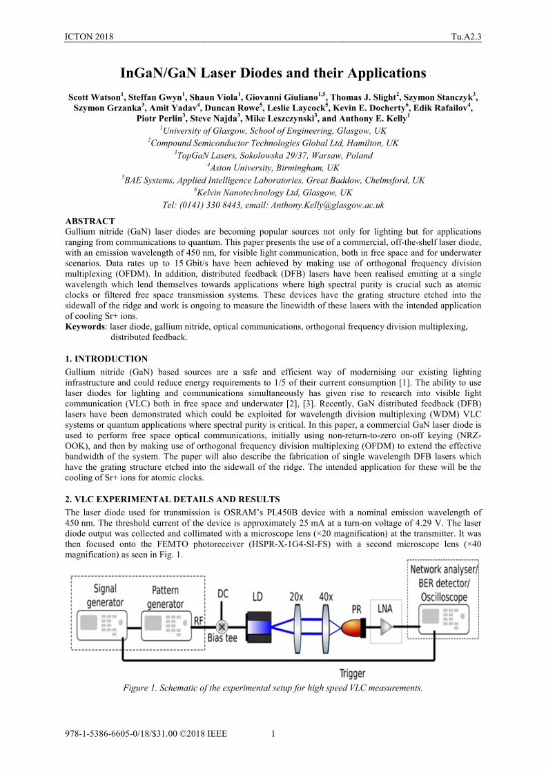
2. VLC EXPERIMENTAL DETAILS AND RESULTSThe laser diode used for transmission is OSRAM’s PL450B device with a nominal emission wavelength of 450 nm. The threshold current of the device is approximately 25 mA at a turn-on voltage of 4.29 V. The laser diode output was collected and collimated with a microscope lens (×20 magnification) at the transmitter. It was then focused onto the FEMTO photoreceiver (HSPR-X-1G4-SI-FS) with a second microscope lens (×40 magnification) as seen in Fig. 1.
Figure 1. Schematic of the experimental setup for high speed VLC measurements.
ICTON 2018 Tu.A2.3
2
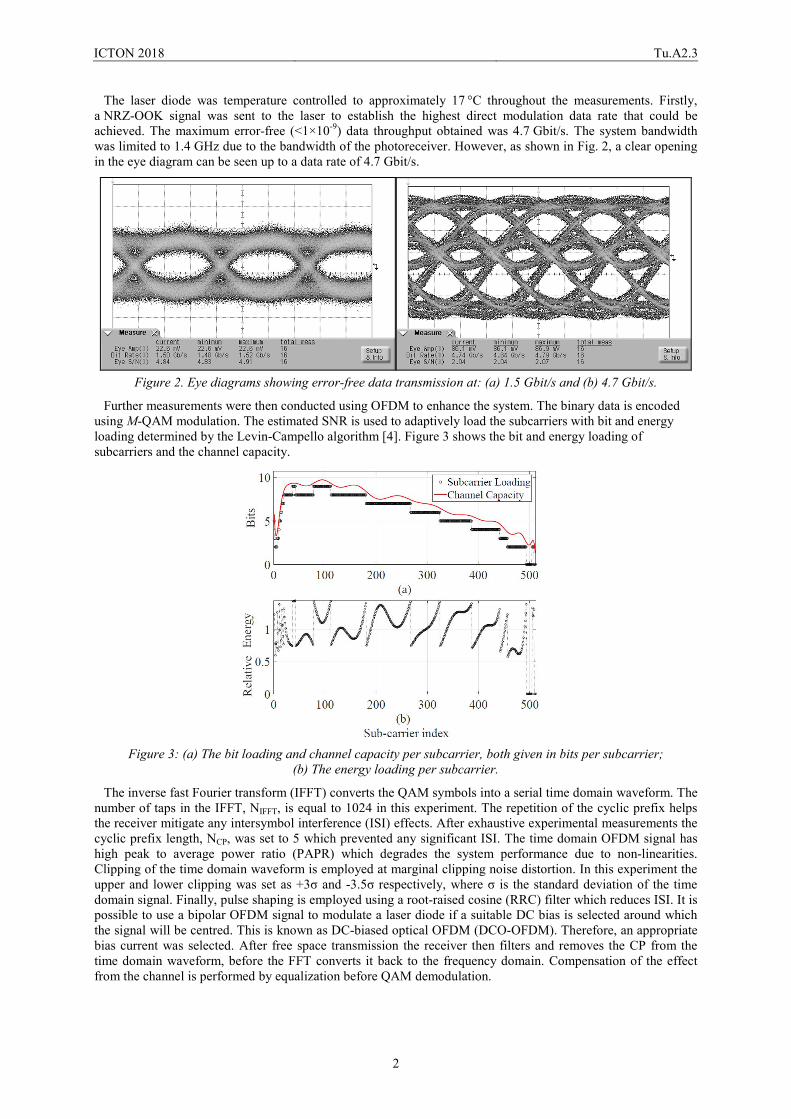
The laser diode was temperature controlled to approximately 17 °C throughout the measurements. Firstly, a NRZ-OOK signal was sent to the laser to establish the highest direct modulation data rate that could be achieved. The maximum error-free (<1×10⁻⁹) data throughput obtained was 4.7 Gbit/s. The system bandwidth was limited to 1.4 GHz due to the bandwidth of the photoreceiver. However, as shown in Fig. 2, a clear opening in the eye diagram can be seen up to a data rate of 4.7 Gbit/s.
Figure 2. Eye diagrams showing error-free data transmission at: (a) 1.5 Gbit/s and (b) 4.7 Gbit/s.
Further measurements were then conducted using OFDM to enhance the system. The binary data is encoded using M-QAM modulation. The estimated SNR is used to adaptively load the subcarriers with bit and energy loading determined by the Levin-Campello algorithm [4]. Figure 3 shows the bit and energy loading of subcarriers and the channel capacity.
Figure 3: (a) The bit loading and channel capacity per subcarrier, both given in bits per subcarrier;
(b) The energy loading per subcarrier.
The inverse fast Fourier transform (IFFT) converts the QAM symbols into a serial time domain waveform. The number of taps in the IFFT, NIFFT, is equal to 1024 in this experiment. The repetition of the cyclic prefix helps the receiver mitigate any intersymbol interference (ISI) effects. After exhaustive experimental measurements the cyclic prefix length, NCP, was set to 5 which prevented any significant ISI. The time domain OFDM signal has high peak to average power ratio (PAPR) which degrades the system performance due to non-linearities. Clipping of the time domain waveform is employed at marginal clipping noise distortion. In this experiment the upper and lower clipping was set as +3σ and -3.5σ respectively, where σ is the standard deviation of the time domain signal. Finally, pulse shaping is employed using a root-raised cosine (RRC) filter which reduces ISI. It is possible to use a bipolar OFDM signal to modulate a laser diode if a suitable DC bias is selected around which the signal will be centred. This is known as DC-biased optical OFDM (DCO-OFDM). Therefore, an appropriate bias current was selected. After free space transmission the receiver then filters and removes the CP from the time domain waveform, before the FFT converts it back to the frequency domain. Compensation of the effect from the channel is performed by equalization before QAM demodulation.

ICTON 2018 Tu.A2.3
3
Figure 4: (a) The SNR across the effective bandwidth for different bias levels over 15 cm link;
(b) Data rate versus BER over 15 cm and 197 cm link.
Figure 4(a) shows the SNR over the 15 cm free space link at different drive currents. Data was transmitted using the optimal modulation voltage of 500 mV at varying drive currents and the MATLAB receiver code measured the end to end system SNR of each subcarrier. It can be seen that by increasing the drive current from 60 mA to 70 mA there is a noticeable improvement in the SNR of the high frequency subcarriers due to the increase in laser bandwidth with current. However, the inset in Fig. 4(a) also details the reduction in SNR at lower subcarriers. It was found that 65 mA was the optimal drive current which resulted in the highest system data rate. Figure 4(b) shows BER versus data rate for the 15 cm free space link. The dashed horizontal line illustrates the BER required to meet the forward error correction (FEC) limit which is 3.8 × 10⁻³. From the figure it can be seen that 15 Gbit/s data transmission can be achieved below the FEC limit. The transmission distance was then increased to 197 cm which was deemed a practical distance for dual purpose lighting VLC systems or remotely operated underwater vehicles. The receiver lens, previously a microscope lens, was replaced with a larger aspheric lens (ACL7560U-A). The laser bias and modulation voltage were unchanged. The maximum successful data rate is reduced to 13.5 Gbit/s due to the increased losses and therefore lower SNR. The relatively small decrease in maximum bit rate for this distance is due to the use of a near collimated laser output which is promising that high data rate transmission over larger distances can be achieved.
3. FABRICATION AND MEASUREMENT OF BLUE DFB LASER There are several approaches that can be taken to fabricate a DFB laser such as buried gratings, surface gratings or shallow etched lateral gratings [5],[6]. However, here sidewall gratings in the InGaN/GaN material system are presented. Both 3rd order and higher order sidewall gratings (39th order) have been fabricated, achieving single wavelength emission [7]. One of the main aims of this work is to develop narrow linewidth (<1 MHz) blue laser operation suitable for implementation in quantum sensors based on ultracold atoms.
Device fabrication was carried out on commercially available GaN laser grade material which consisted of three InGaN quantum wells with GaN barriers. Similar steps are taken in the fabrication process for both 3rd order and higher order gratings. Grating and ridge patterns were defined in ZEP 520 resist using electron beam lithography (EBL). The EBL tool used (Vistech VB6 UHR) has a write resolution of 1 nm, enabling the emission wavelength to be targeted accurately. Reactive ion etching on an STS Multiplex tool was then used to form the grating and ridge. A Cl2/N2 based ICP etch process with 300 W platen and 600 W coil power produced the vertical and smooth etch profile required for good grating performance. Electron micrographs of the 3rd and 39th order gratings can be seen in Fig. 5.
Figure 5. SEM image of: (a) the etched 3rd order grating and (b) the etched 39th order grating.
Both the 3rd order and 39th order grating structures have been tested and show good single wavelength operation. More details can be found in [7], [8].
ICTON 2018 Tu.A2.3
4
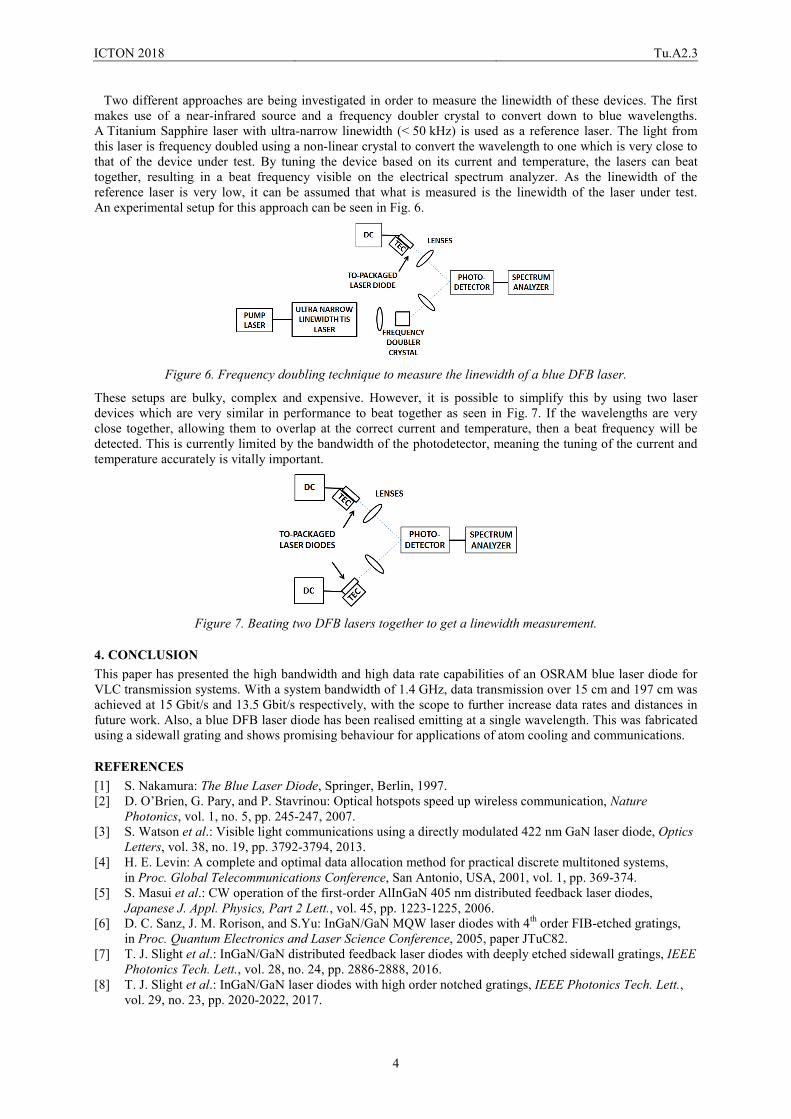
Two different approaches are being investigated in order to measure the linewidth of these devices. The first makes use of a near-infrared source and a frequency doubler crystal to convert down to blue wavelengths. A Titanium Sapphire laser with ultra-narrow linewidth (< 50 kHz) is used as a reference laser. The light from this laser is frequency doubled using a non-linear crystal to convert the wavelength to one which is very close to that of the device under test. By tuning the device based on its current and temperature, the lasers can beat together, resulting in a beat frequency visible on the electrical spectrum analyzer. As the linewidth of the reference laser is very low, it can be assumed that what is measured is the linewidth of the laser under test. An experimental setup for this approach can be seen in Fig. 6.
Figure 6. Frequency doubling technique to measure the linewidth of a blue DFB laser.
These setups are bulky, complex and expensive. However, it is possible to simplify this by using two laser devices which are very similar in performance to beat together as seen in Fig. 7. If the wavelengths are very close together, allowing them to overlap at the correct current and temperature, then a beat frequency will be detected. This is currently limited by the bandwidth of the photodetector, meaning the tuning of the current and temperature accurately is vitally important.
Figure 7. Beating two DFB lasers together to get a linewidth measurement.
4. CONCLUSION This paper has presented the high bandwidth and high data rate capabilities of an OSRAM blue laser diode for VLC transmission systems. With a system bandwidth of 1.4 GHz, data transmission over 15 cm and 197 cm was achieved at 15 Gbit/s and 13.5 Gbit/s respectively, with the scope to further increase data rates and distances in future work. Also, a blue DFB laser diode has been realised emitting at a single wavelength. This was fabricated using a sidewall grating and shows promising behaviour for applications of atom cooling and communications.
REFERENCES [1] S. Nakamura: The Blue Laser Diode, Springer, Berlin, 1997. [2] D. O’Brien, G. Pary, and P. Stavrinou: Optical hotspots speed up wireless communication, Nature
Photonics, vol. 1, no. 5, pp. 245-247, 2007. [3] S. Watson et al.: Visible light communications using a directly modulated 422 nm GaN laser diode, Optics
Letters, vol. 38, no. 19, pp. 3792-3794, 2013. [4] H. E. Levin: A complete and optimal data allocation method for practical discrete multitoned systems,
in Proc. Global Telecommunications Conference, San Antonio, USA, 2001, vol. 1, pp. 369-374. [5] S. Masui et al.: CW operation of the first-order AlInGaN 405 nm distributed feedback laser diodes,
Japanese J. Appl. Physics, Part 2 Lett., vol. 45, pp. 1223-1225, 2006. [6] D. C. Sanz, J. M. Rorison, and S.Yu: InGaN/GaN MQW laser diodes with 4th order FIB-etched gratings,
in Proc. Quantum Electronics and Laser Science Conference, 2005, paper JTuC82. [7] T. J. Slight et al.: InGaN/GaN distributed feedback laser diodes with deeply etched sidewall gratings, IEEE
Photonics Tech. Lett., vol. 28, no. 24, pp. 2886-2888, 2016. [8] T. J. Slight et al.: InGaN/GaN laser diodes with high order notched gratings, IEEE Photonics Tech. Lett.,
vol. 29, no. 23, pp. 2020-2022, 2017.