influence of temperature reaction for the cdse–tio2
TRANSCRIPT

materials
Article
Influence of Temperature Reaction for theCdSe–TiO2 Nanotube Thin Film Formation viaChemical Bath Deposition in Improving thePhotoelectrochemical Activity
Chin Wei Lai 1,* , Nurul Asma Samsudin 2,*, Foo Wah Low 2,* , Nur Azimah Abd Samad 1,Kung Shiuh Lau 1, Pui May Chou 3, Sieh Kiong Tiong 2 and Nowshad Amin 2,4
1 Level 3, Block A, Nanotechnology & Catalysis Research Centre (NANOCAT), Institute for AdvancedStudies (IAS), University of Malaya, Kuala Lumpur 50603, Malaysia; [email protected] (N.A.A.S.);[email protected] (K.S.L.)
2 Institute of Sustainable Energy (ISE), Universiti Tenaga Nasional (The Energy University), JalanIKRAM-UNITEN, Kajang 43000, Selangor, Malaysia; [email protected] (S.K.T.);[email protected] (N.A.)
3 School of Engineering, Faculty of Built Environment Engineering, Technology & Design, Taylor’s LakesideCampus, No. 1, Jalan Taylors, Subang Jaya 47500, Malaysia; [email protected]
4 Department of Electrical, Electronic and Systems Engineering, Faculty of Engineering and BuiltEnvironment, Universiti Kebangsaan Malaysia (National University of Malaysia), Bangi 43600, Malaysia
* Correspondence: [email protected] (C.W.L.); [email protected] (N.A.S.);[email protected] (F.W.L.); Tel.: +603-79676959 (ext. 2925) (C.W.L.)
Received: 6 February 2020; Accepted: 4 March 2020; Published: 3 June 2020�����������������
Abstract: In this present work, we report the deposition of cadmium selenide (CdSe) particles ontitanium dioxide (TiO2) nanotube thin films, using the chemical bath deposition (CBD) method atlow deposition temperatures ranging from 20 to 60 ◦C. The deposition temperature had an influenceon the overall CdSe–TiO2 nanotube thin film morphologies, chemical composition, phase transition,and optical properties, which, in turn, influenced the photoelectrochemical performance of thesamples that were investigated. All samples showed the presence of CdSe particles in the TiO2
nanotube thin film lattice structures with the cubic phase CdSe compound. The amount of CdSeloading on the TiO2 nanotube thin films were increased and tended to form agglomerates as a functionof deposition temperature. Interestingly, a significant enhancement in photocurrent density wasobserved for the CdSe–TiO2 nanotube thin films deposited at 20 ◦C with a photocurrent density of1.70 mA cm−2, which was 17% higher than the bare TiO2 nanotube thin films. This sample showed aclear surface morphology without any clogged nanotubes, leading to better ion diffusion, and, thus,an enhanced photocurrent density. Despite having the least CdSe loading on the TiO2 nanotubethin films, the CdSe–TiO2 nanotube thin films deposited at 20 ◦C showed the highest photocurrentdensity, which confirmed that a small amount of CdSe is enough to enhance the photoelectrochemicalperformance of the sample.
Keywords: electrochemical anodization; chemical bath deposition; photoelectrochemical activity;cadmium selenide; CdSe–TiO2 nanotube thin films
1. Introduction
Nanostructured titanium dioxide (TiO2) has been known as one of the most promisingsemiconductor materials, as it has been widely used in many applications, such as photocatalysts [1–4],photovoltaics [5–11], photoelectrochemical cells [12–15], supercapacitors [16–19], and sensors [20],
Materials 2020, 13, 2533; doi:10.3390/ma13112533 www.mdpi.com/journal/materials

Materials 2020, 13, 2533 2 of 16
due to its remarkable chemical, optical, and physical properties, as well as its low production costand lower toxicity. The electrochemical anodization method has come to light, as it is proven to bethe most facile and versatile method to synthesized TiO2 nanotube thin films due to its ability tomodify the morphology, diameter, and length of the nanotubes by varying the anodization parameters.In addition, their unique nanoarchitecture minimizes the photo-induced charge of the recombinationloss of the carrier at the nanostructure connections, thus, maximizing photon absorption [21,22].However, due to its wide band gap (3.2 eV for the anatase phase and 3.0 for the rutile phase TiO2),the adsorption by the material is limited to UV wavelength [23]. Moreover, the fast electron/holerecombination and sluggish charge transfer by the TiO2 nanotube thin films significantly demeritthe photoelectrochemical performance of this material [24]. In order to overcome the limitations,modification, such as electrochemical reduction [25,26], metal oxide heterojunction [27,28], defectengineering [29], and metal or non-metal doping [30–33], have been done to lower the band gap ofthe TiO2 nanotube thin films and, thus, enhance the conductivity, radiation adsorption, and catalyticactivity, respectively. The deposition of small band gap semiconductor materials as a sensitizer on theTiO2 nanotube thin films [34–36] have been proven to be an important approach in order to tune theoverall band gap of the material and improve its photoelectrochemical performance. By incorporatingthese materials on the TiO2 nanotube thin films, the further enhancement of the adsorption of visiblelight and fastening the charge transfer of photoexcited electrons into the TiO2 conduction bandis needed.
Cadmium selenide (CdSe) is one of most remarkable semiconductor materials in Group II–VI, thatis being used to sensitize wide band gap TiO2 nanotube thin films [23,37]. The CdSe has a lower bandedge than TiO2, thus, allowing band edge alignment, leading to efficient electron transfer. The bandedge alignment effect will improve photo-illumination absorption at visible or near-IR photons andeventually reduce the recombination change carrier losses [38–40]. There are several methods thathave been used to incorporate CdSe on the nanostructured TiO2, which is functional under highlycontrolled conditions [41–44]. Among the deposition method, chemical bath deposition (CBD) is one ofthe methods that has been widely used to deposit CdSe particles on the TiO2 nanotube thin films [45].This method becomes favourable, as it uses simple equipment and apparatus, making this methodcost-effective. Our previous report shows that by tuning the parameters of the CBD, the morphologyand other physical properties of the CdSe–TiO2 nanotube thin films can be altered, thus, enhancingthe photoelectrochemical performance of the sample [37,46]. Despite many reports on the aim toincrease the performance of CdSe–TiO2 nanotube thin films as photoelectrochemical cells, it is crucial tostudy the deposition parameters, which influence the chemical and physical properties of CdSe–TiO2
nanotube thin films.The CBD of CdSe used in this work could offer good controls of amount loading, size, and
uniformity of CdSe on the TiO2 nanotube thin films. Parameters, such as the temperature of the CBD,becomes a crucial role in manipulating the thermal dislocation of the Cd complex and Se anion bycontrolling the rate of ions released from the precursor, and thereby affecting the growth rate of CdSe onthe TiO2 nanotubes thin films. With increasing temperature, thermal dissociation of the CdSe precursoris used in this study: sodium selenosulfate (Na2SeSO3) and cadmium acetate dihydrate (Cd(CH3COO)2
2H2O) will be increased significantly. Henceforth, increasing the kinetic energy and driving force of theactive precursor leads to the increase of interaction between CdSe and nanotubular structures. Last butnot least, a comprehensive study has been conducted that aims to optimize the temperature of the CBDof CdSe on the TiO2 nanotube thin films in order to enhance their photoelectrochemical performance.
2. Experimental Section
2.1. Preparation of TiO2 Nanotube Thin Films
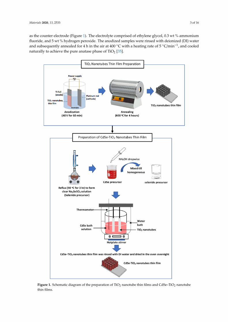
The TiO2 nanotube thin films were prepared by the electrochemical method of anodizing Ti foilsin a two-electrode cell at 40 V for 60 min, consisting of Ti foil as the working electrode and platinum rod
Materials 2020, 13, 2533 3 of 16
as the counter electrode (Figure 1). The electrolyte comprised of ethylene glycol, 0.3 wt % ammoniumfluoride, and 5 wt % hydrogen peroxide. The anodized samples were rinsed with deionized (DI) waterand subsequently annealed for 4 h in the air at 400 ◦C with a heating rate of 5 ◦C/min−1, and coolednaturally to achieve the pure anatase phase of TiO2 [35].Materials 2020, 13, x FOR PEER REVIEW 4 of 17
Figure 1. Schematic diagram of the preparation of TiO2 nanotube thin films and CdSe–TiO2 nanotube thin films.
Figure 1. Schematic diagram of the preparation of TiO2 nanotube thin films and CdSe–TiO2 nanotubethin films.

Materials 2020, 13, 2533 4 of 16
2.2. Preparation of CdSe–TiO2 Nanotube Thin Films
The CdSe was deposited on the TiO2 nanotube thin films via CBD, as shown in the schematicdiagram in Figure 1. To prepare the 5 mM CdSe solution precursor, the selenide precursor (Na2SeSO3
solution) was prepared by mixing 0.6 M sodium sulfite with 0.2 M selenium metal powder in DI water.The mixture was heated under reflux at 90 ◦C for 3 h to form a clear Na2SeSO3 solution. The cadmiumprecursor was prepared by dissolving 0.2 M of Cd(CH3COO)2·2H2O in DI water. Then, a concentratedammonia solution (30%) was added into the cadmium solution slowly to adjust the pH of the solutionbetween 12 to 12.5. This was to prevent a reverse reaction of Cd(NH3)4
2+ to form stable cadmiumhydroxide (Cd(OH)2). Both precursor solutions were then mixed until homogenous. The annealedanatase TiO2 nanotube thin films were soaked vertically inclined into the CdSe bath solution forthe deposition process for 1 h. The deposition temperature was varied from 20 to 60 ◦C. A digitalprogrammable hotplate (Torrey Pines Scientific) was used in this experiment. The temperature of thechemical bath was set and, upon the deposition process, the solution’s temperature was checked, usinga thermometer for confirmation. Throughout the deposition process, the temperature of the chemicalbath was checked from time to time. Then, the samples were the rinsed with DI water and dried in anoven overnight.
2.3. Characterizations
The surface and cross-sectional morphologies of the prepared samples (TiO2 nanotube thin filmsand CdSe/TiO2 nanotube thin films) were investigated via field emission scanning electron microscopy(FE-SEM, JEO JSM 7600-F, JOEL Ltd., Tokyo, Japan) while the elemental analysis was conducted usingOxford Instruments by means of energy dispersive X-ray spectroscopy (EDX, Oxford Instruments,Abingdon, United Kingdom) The phase transition and crystallinity of all prepared samples was studiedusing X-ray diffraction (XRD, Bruker AXS D8 Advance, Bruker, Karlsruhe, Germany)and a Ramanspectrometer (Renishaw inVia, Renishaw, Wotton-under-Edge, United Kingdom)In this study, XRD wasoperated using Cu Kα radiation (λ = 0.1546 nm) at a scanning rate of 2◦ min−1 over the angles 2θ = 20◦
to 70◦. The Raman spectroscopy was operated at an excitation wavelength of 532 nm generated byan Ar ion laser over the range of 100 to 1000 cm−1. The binding energy and chemical state of thesamples were measured and quantified with X-ray photoelectron spectroscopy (XPS, PHI Quantera II,Physical Electronic, Minnesota, USA) with an Al cathode scan (hv = 1486.8 eV) of 100 microns and280 eV with pass energy. The precise analysis of the features of each element was decomposed inthe Shirley background using the Voigt curve fitting function. The optical properties of the preparedsamples were recorded using a UV-Vis diffused reflectance spectrophotometer (Shimadzu UV-2700UV-Vis, Shimadzu, Kyoto, Tokyo) from 240 to 800 nm.
2.4. Photoelectrochemical Testing
A three-electrode system composed of Pt as the counter electrode, Ag/AgCl (3 M KCl) as thereference electrode, and the prepared samples as the working electrode were used in a 1 M KOHaqueous electrolyte. The photoelectrochemical measurement of the prepared samples was evaluated bylinear sweep voltammetry using a potantiostat (Autolab PGSTAT 204, Metrohm, Herisau, Switzerland)and illuminated by a 150 W Xenon lamp (Zolix LSP-X150, Zolix Instruments CO., Ltd., Beijing, China)with a light intensity of 100 mW cm−2 focusing on the dipped part of the electrode.
3. Results and Discussion
The surface and cross-section morphologies of all the prepared CdSe–TiO2 nanotube thin filmsamples deposited at various temperatures from 20 to 60 ◦C are shown in Figure 2a–d. The highlyordered TiO2 nanotube thin films were successfully synthesized in our previous report, with an averageinner-tube diameter and tube length of 76 nm and 5.6 µm, respectively [21,47]. In this study, a clearsurface morphology change was observed for all samples as function to the chemical bath temperature.

Materials 2020, 13, 2533 5 of 16
At a low temperature (20 ◦C), the deposition of CdSe on the TiO2 nanotube thin films was almostnegligible, as shown in Figure 2a. However, the average inner-tube’s diameter of the sample decreasedto 71 nm upon the deposition of CdSe, indicating that the nucleation process had taken place on thesample. A low chemical bath temperature of 20 ◦C led to a low deposition rate, thus, slowing thenuclei growth on the TiO2 nanotube thin films. As the chemical bath temperature increased to 40 ◦C,the presence of CdSe particles was observed, with an average inner-tube diameter of 90 nm, whichpartially covered the nanotubes (refer to Figure 2b). Moreover, the tube’s diameter decreased to 68 nmupon the deposition of CdSe on the TiO2 nanotube thin films. The agglomeration of CdSe into largerparticles was observed when the chemical bath temperature increased to 50 and 60 ◦C. They wereuniformly dispersed on the surface of the nanotubes with an average diameter of 145 nm at chemicalbath temperatures of 50 ◦C and 220 nm at 60 ◦C. Furthermore, the agglomeration of CdSe coveredmost of the nanotube circumferences, as shown in Figure 2c–d. The average tube diameters of thesamples were found to decrease to 57 nm (50 ◦C) and 54 nm (60 ◦C). The cross-sectional morphologies(inset figures) showed an adhesive texture, with the presence of CdSe particles deposited throughoutthe wall surface. This indicates that the deposition of CdSe took place on the top surface and the wallsurface of the nanotubes. The EDX analysis confirmed the presence of cadmium (Cd), selenium (Se),titanium (Ti), and oxygen (O) elements in all samples, as shown in Table 1. These results supportedthe observation from the FE-SEM results, as the elemental composition of Cd and Se increased as thechemical bath temperature increased. In addition, the ratio of the Cd and Se elements in all sampleswas 1:1, thereby confirming the deposition of stoichiometry CdSe on the TiO2 nanotube thin films.
Materials 2020, 13, x FOR PEER REVIEW 6 of 17
composition of Cd and Se increased as the chemical bath temperature increased. In addition, the ratio of the Cd and Se elements in all samples was 1:1, thereby confirming the deposition of stoichiometry CdSe on the TiO2 nanotube thin films.
Figure 2. FE-SEM images of CdSe–TiO2 nanotube thin films deposited at chemical batch temperatures of: (a) 20 °C, (b) 40 °C, (c) 50 °C, and (d) 60 °C, and the inset is cross-sectional view.
Table 1. An average at % of CdSe–TiO2 nanotube thin films deposited at different chemical bath temperatures, obtained by energy dispersive X-ray spectroscopy (EDX) analysis.
Temperature (°C) Atomic percentage (at %)
Ti O Cd Se 20 40.77 58.45 0.41 0.37 40 39.62 56.66 1.90 1.82 50 38.16 55.84 3.03 2.97 60 36.27 51.83 6.04 5.86
Figure 3 shows the XRD patterns for the CdSe–TiO2 nanotube thin films deposited at different chemical bath temperatures at 2θ = 20° to 70°. All samples exhibited an intense peak of CdSe at 2θ = 25.35°, which corresponded to the (1 1 1) preferred orientation of a cubic phase of CdSe (JCPDS No.: 19–0191). This peak was found to overlap with the peak of the anatase crystal plane at 2θ = 25.37° (1 0 1) phase. The intensity of the peak increased as function of the chemical bath temperature, which indicated an abundancy of the CdSe and the well crystalline nature of the CdSe [44]. These results were agreeable with the FE-SEM analysis, as the chemical bath temperature increased as the amount of CdSe deposited onto the TiO2 nanotube thin films increased. A small peak was observed at 2θ = 49.7°, corresponding to a (3 1 1) plane of cubic zinc blended phase CdSe in the CdSe–TiO2 nanotube thin films deposited at the chemical bath temperatures of 50 and 60 °C. However, the peak was not
Figure 2. FE-SEM images of CdSe–TiO2 nanotube thin films deposited at chemical batch temperaturesof: (a) 20 ◦C, (b) 40 ◦C, (c) 50 ◦C, and (d) 60 ◦C, and the inset is cross-sectional view.

Materials 2020, 13, 2533 6 of 16
Table 1. An average at % of CdSe–TiO2 nanotube thin films deposited at different chemical bathtemperatures, obtained by energy dispersive X-ray spectroscopy (EDX) analysis.
Temperature (◦C)Atomic Percentage (at %)
Ti O Cd Se
20 40.77 58.45 0.41 0.3740 39.62 56.66 1.90 1.8250 38.16 55.84 3.03 2.9760 36.27 51.83 6.04 5.86
Figure 3 shows the XRD patterns for the CdSe–TiO2 nanotube thin films deposited at differentchemical bath temperatures at 2θ = 20◦ to 70◦. All samples exhibited an intense peak of CdSe at2θ = 25.35◦, which corresponded to the (1 1 1) preferred orientation of a cubic phase of CdSe (JCPDSNo.: 19-0191). This peak was found to overlap with the peak of the anatase crystal plane at 2θ = 25.37◦
(1 0 1) phase. The intensity of the peak increased as function of the chemical bath temperature, whichindicated an abundancy of the CdSe and the well crystalline nature of the CdSe [44]. These resultswere agreeable with the FE-SEM analysis, as the chemical bath temperature increased as the amount ofCdSe deposited onto the TiO2 nanotube thin films increased. A small peak was observed at 2θ = 49.7◦,corresponding to a (3 1 1) plane of cubic zinc blended phase CdSe in the CdSe–TiO2 nanotube thin filmsdeposited at the chemical bath temperatures of 50 and 60 ◦C. However, the peak was not detected inthe CdSe–TiO2 nanotube thin films deposited at low chemical bath temperatures due to the low contentof CdSe (< 2 at % from EDX analysis) in the sample, which was too insufficient to be detected by XRDanalysis [48–50]. The single phase of TiO2 crystal indexed to anatase planes (JCPDS No.: 21–1272)was observed at 2θ = 38.67◦, 48.21◦, 54.10◦, 55.26◦, 62.66◦, and 68.74◦, corresponding respectively toplanes (1 1 2), (2 0 0), (1 0 5), (2 1 1), (2 0 4), and (1 1 6). In addition, the peaks at 2θ = 35.1◦, 38.4◦,40.2◦, and 53.0◦ corresponded to (1 0 0), (0 0 2), (1 0 1), and (1 0 2), and were originated from a Ti metalsubstrate (JCPDS no.: 44-1294).
Materials 2020, 13, x; doi: FOR PEER REVIEW www.mdpi.com/journal/materials
Figure 3. XRD diffraction patterns of CdSe–TiO2 nanotube thin films soaked at (a) 20 °C, (b) 40 °C, (c) 50 °C, and (d) 60 °C in 5 mM CdSe bath solution for 1 h (A = anatase TiO2, T = Ti metal).
Figure 3. XRD diffraction patterns of CdSe–TiO2 nanotube thin films soaked at (a) 20 ◦C, (b) 40 ◦C,(c) 50 ◦C, and (d) 60 ◦C in 5 mM CdSe bath solution for 1 h (A = anatase TiO2, T = Ti metal).

Materials 2020, 13, 2533 7 of 16
The Raman spectra of the CdSe–TiO2 nanotube thin films (shown in Figure 4) further confirmedthe presence of cubic CdSe phase in the samples. The characteristic peaks of the anatase phase of TiO2
were observed at 144, 394, 515, and 636 cm−1, corresponding to Eg, B1g, A1g, and Eg vibration modes.The Eg vibration mode was mainly caused by symmetric stretching vibration, while B1g was due tothe symmetric bending vibration, and A1g was caused by the anti-symmetric bending of O–Ti–O inTiO2 [46,51]. A gradual decrease in the intensity of these peaks was observed with an increase of thechemical bath temperature due to the increase of cubic CdSe content in the samples. The samplesprepared at chemical bath temperatures of 40, 50, and 60 ◦C showed presence of a Raman shift at206 cm−1, corresponding to the first order for the longitudinal optical phonon (LO) of cubic CdSe.Materials 2020, 13, x FOR PEER REVIEW 2 of 2
Figure 4. Raman spectrum of CdSe–TiO2 nanotube thin films soaked at (a) 20 °C, (b) 40 °C, (c) 50 °C, and (d) 60 °C in 5 mM CdSe solution for 1 h.
Figure 4. Raman spectrum of CdSe–TiO2 nanotube thin films soaked at (a) 20 ◦C, (b) 40 ◦C, (c) 50 ◦C,and (d) 60 ◦C in 5 mM CdSe solution for 1 h.
The surface chemical state of pure TiO2 nanotube thin films and CdSe–TiO2 nanotube thin filmswas investigated using XPS analysis. Figure 5 displays the XPS spectra of both samples, which mainlyconsisted of Ti 2p, O 1s, Cd 3d, and Se 3d elements. Two broad peaks centered at 458.80 and 464.50 eVare observed in Figure 4a, corresponding to the Ti 2p3/2 and Ti 2p1/2 peaks of Ti4+ in the TiO2 nanotubethin films [39]. The intensity of both peaks gradually decreased upon the deposition of CdSe intothe TiO2 nanotube thin films, indicating the presence of CdSe in the TiO2 lattice structure. However,the deposition of CdSe on TiO2 did not affect the Ti chemical state of the nanotubes. In contrast, theO 1s elements showed a slight shift from 530.90 eV for the pure TiO2 nanotube thin film samples to529.90 eV for the CdSe–TiO2 nanotube thin film samples due the strong interaction between CdSeclusters and TiO2 nanotube thin films. The strong interaction bond between CdSe and TiO2 served asthe heterojunctions that became captives of the electron/hole pairs from the CdSe clusters [38]. Hence,this will suppress the recombination of the electron/hole and photoelectrochemical activity.

Materials 2020, 13, 2533 8 of 16Materials 2020, 13, x FOR PEER REVIEW 9 of 17
Figure 5. High-resolution XPS spectra of (a) Ti 2p, (b) O 1s, (c) Cd 3d, and (d) Se 3d of pure TiO2 nanotube thin films and CdSe–TiO2 nanotube thin films.
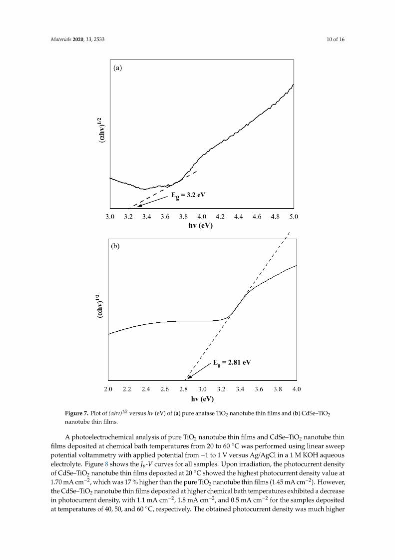
The optical properties of pure TiO2 nanotube thin films and CdSe–TiO2 nanotube thin films were carried out using a UV-Vis diffuse reflectance analysis (DRS). The adsorption spectra for both samples are shown in Figure 6. The adsorption edge of pure TiO2 nanotube thin films was observed below 400 nm due to the excitation of the electron from the valence band to the conduction band [54]. However, the CdSe–TiO2 nanotube thin films showed an adsorption above 400 nm, suggesting that more visible light was adsorbed by the sample, hence facilitating the generation of a high amount of carrier charge, which then enhanced the photocurrent response of the sample. The Tauc approach was used to determine the optical bandgap of the pure TiO2 nanotube thin films and CdSe–TiO2 nanotube thin film samples using the equation below:
(1)
where Eg is the separation between the bottom of the conduction band and the top of the valance band, hv is the photon energy, and n is the constant. In this case, n = ½, which follows a direct transition. The plot of (αhv)1/2 against hv for the pure TiO2 nanotube thin films and CdSe–TiO2 nanotube thin films are shown in Figure 7. The band gap of pure TiO2 nanotube thin films and CdSe–
Figure 5. High-resolution XPS spectra of (a) Ti 2p, (b) O 1s, (c) Cd 3d, and (d) Se 3d of pure TiO2
nanotube thin films and CdSe–TiO2 nanotube thin films.
Figure 5c illustrates the double peak features of the Cd 3d spectra for the CdSe–TiO2 nanotubethin film sample, suggesting the presence of Cd element in the sample, while no traces of Cd elementwere observed in the TiO2 nanotube thin film sample. The precise assessment of the functionsof the spin-orbital split Cd 3d5/2 and Cd 3d3/2 were disintegrated by using the Voigt curve fittingfunction within the Shirley background. Four peaks were observed, centered at 405.13 and 404.59 eVcorresponding to Cd 3d5/2, whereas the binding energy at 411.98 and 411.40 eV corresponded to Cd3d3/2. The prominent binding energy centered at 405.13 and 411.98 eV, which was due to the core levelof Cd2+ cations of the CdSe crystal structure [41]. The additional peaks observed with lower intensitiesof 405.13 and 411.98 had a weak shift in peak positions. CdO formation was also proved in CdSe, wherethe core levels of the oxidation of Cd were weak at the 3d5/2 and 3d3/2 core levels [51,52]. The smallCdO volume could, therefore, be verifiable using the CBD technique from low intensity peaks with404.59 and 411.40 bonding energy. The existence of the Se element in the CdSe–TiO2 nanotube thinfilms sample was proved from the Se 3d spectra shown in Figure 5d. A broad peak centered at 54.46 eVrepresented that the Se 3d3/2 characteristic was due to the Se2− anions of CdSe [53,54].

Materials 2020, 13, 2533 9 of 16
The optical properties of pure TiO2 nanotube thin films and CdSe–TiO2 nanotube thin filmswere carried out using a UV-Vis diffuse reflectance analysis (DRS). The adsorption spectra for bothsamples are shown in Figure 6. The adsorption edge of pure TiO2 nanotube thin films was observedbelow 400 nm due to the excitation of the electron from the valence band to the conduction band [54].However, the CdSe–TiO2 nanotube thin films showed an adsorption above 400 nm, suggesting thatmore visible light was adsorbed by the sample, hence facilitating the generation of a high amount ofcarrier charge, which then enhanced the photocurrent response of the sample. The Tauc approach wasused to determine the optical bandgap of the pure TiO2 nanotube thin films and CdSe–TiO2 nanotubethin film samples using the equation below:
α =α0√
hv− Eg
hv(1)
where Eg is the separation between the bottom of the conduction band and the top of the valance band,hv is the photon energy, and n is the constant. In this case, n = 1
2 , which follows a direct transition.The plot of (αhv)1/2 against hv for the pure TiO2 nanotube thin films and CdSe–TiO2 nanotube thinfilms are shown in Figure 7. The band gap of pure TiO2 nanotube thin films and CdSe–TiO2 nanotubethin films were estimated from the intersection of the baseline with the tangent line of the sharplydecreasing region of the spectra. It was noted that the band gap of the pure TiO2 nanotube thin filmswas 3.20 eV, while the band gap of the CdSe–TiO2 nanotube thin films was 2.81 eV. It was well knownthat the CdSe bulk sample band gap was 1.74 eV. Typically, the band gap of CdSe varies with thedeposition method and deposition parameters, and is also attributed due to the changes in the filmcomposition and structural defects. In this case, the large band gap of the CdSe–TiO2 nanotube thinfilms corresponded to the low amount of CdSe on the TiO2 nanotube thin films, as discussed in theEDX results.
Materials 2020, 13, x FOR PEER REVIEW 10 of 17
TiO2 nanotube thin films were estimated from the intersection of the baseline with the tangent line of the sharply decreasing region of the spectra. It was noted that the band gap of the pure TiO2 nanotube thin films was 3.20 eV, while the band gap of the CdSe–TiO2 nanotube thin films was 2.81 eV. It was well known that the CdSe bulk sample band gap was 1.74 eV. Typically, the band gap of CdSe varies with the deposition method and deposition parameters, and is also attributed due to the changes in the film composition and structural defects. In this case, the large band gap of the CdSe–TiO2 nanotube thin films corresponded to the low amount of CdSe on the TiO2 nanotube thin films, as discussed in the EDX results.
Figure 6. Absorption patterns for (a) CdSe–TiO2 nanotube thin films subjected to 20 °C soaking temperature and (b) pure TiO2 nanotube thin films.
300 400 500 600 700 800
Abs
orba
nce
(a.u
.)
Wavelength (nm)
(b)
(a)
3.0 3.2 3.4 3.6 3.8 4.0 4.2 4.4 4.6 4.8 5.0
(αhv
)1/2
hv (eV)
Eg = 3.2 eV
(a)
Figure 6. Absorption patterns for (a) CdSe–TiO2 nanotube thin films subjected to 20 ◦C soakingtemperature and (b) pure TiO2 nanotube thin films.
Materials 2020, 13, 2533 10 of 16
Materials 2020, 13, x FOR PEER REVIEW 10 of 17
TiO2 nanotube thin films were estimated from the intersection of the baseline with the tangent line of the sharply decreasing region of the spectra. It was noted that the band gap of the pure TiO2 nanotube thin films was 3.20 eV, while the band gap of the CdSe–TiO2 nanotube thin films was 2.81 eV. It was well known that the CdSe bulk sample band gap was 1.74 eV. Typically, the band gap of CdSe varies with the deposition method and deposition parameters, and is also attributed due to the changes in the film composition and structural defects. In this case, the large band gap of the CdSe–TiO2 nanotube thin films corresponded to the low amount of CdSe on the TiO2 nanotube thin films, as discussed in the EDX results.
Figure 6. Absorption patterns for (a) CdSe–TiO2 nanotube thin films subjected to 20 °C soaking temperature and (b) pure TiO2 nanotube thin films.
300 400 500 600 700 800
Abs
orba
nce
(a.u
.)
Wavelength (nm)
(b)
(a)
3.0 3.2 3.4 3.6 3.8 4.0 4.2 4.4 4.6 4.8 5.0
(αhv
)1/2
hv (eV)
Eg = 3.2 eV
(a)
Materials 2020, 13, x FOR PEER REVIEW 11 of 17
Figure 7. Plot of (αhν)1/2 versus hν (eV) of (a) pure anatase TiO2 nanotube thin films and (b) CdSe–TiO2
nanotube thin films.
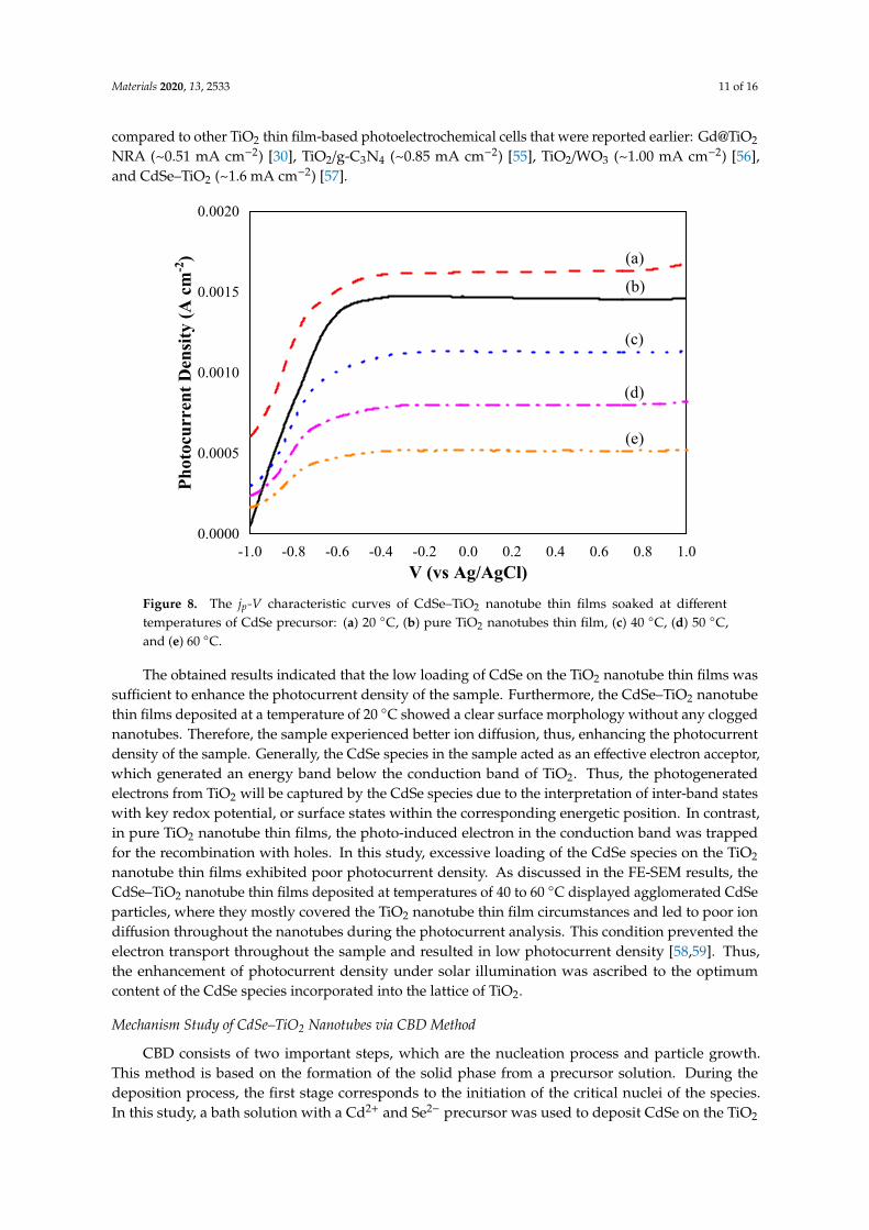
A photoelectrochemical analysis of pure TiO2 nanotube thin films and CdSe–TiO2 nanotube thin films deposited at chemical bath temperatures from 20 to 60 °C was performed using linear sweep potential voltammetry with applied potential from −1 to 1 V versus Ag/AgCl in a 1 M KOH aqueous electrolyte. Figure 8 shows the Jp-V curves for all samples. Upon irradiation, the photocurrent density of CdSe–TiO2 nanotube thin films deposited at 20 °C showed the highest photocurrent density value at 1.70 mA cm−2, which was 17 % higher than the pure TiO2 nanotube thin films (1.45 mA cm−2). However, the CdSe–TiO2 nanotube thin films deposited at higher chemical bath temperatures exhibited a decrease in photocurrent density, with 1.1 mA cm−2, 1.8 mA cm−2, and 0.5 mA cm−2 for the samples deposited at temperatures of 40, 50, and 60 °C, respectively. The obtained photocurrent density was much higher compared to other TiO2 thin film-based photoelectrochemical cells that were reported earlier: Gd@TiO2 NRA (~0.51 mA cm−2) [30], TiO2/g-C3N4 (~0.85 mA cm−2) [55], TiO2/WO3 (~1.00 mA cm−2) [56], and CdSe–TiO2 (~1.6 mA cm−2) [57].
The obtained results indicated that the low loading of CdSe on the TiO2 nanotube thin films was sufficient to enhance the photocurrent density of the sample. Furthermore, the CdSe–TiO2 nanotube thin films deposited at a temperature of 20 °C showed a clear surface morphology without any clogged nanotubes. Therefore, the sample experienced better ion diffusion, thus, enhancing the photocurrent density of the sample. Generally, the CdSe species in the sample acted as an effective electron acceptor, which generated an energy band below the conduction band of TiO2. Thus, the photogenerated electrons from TiO2 will be captured by the CdSe species due to the interpretation of inter-band states with key redox potential, or surface states within the corresponding energetic position. In contrast, in pure TiO2 nanotube thin films, the photo-induced electron in the conduction band was trapped for the recombination with holes. In this study, excessive loading of the CdSe species on the TiO2 nanotube thin films exhibited poor photocurrent density. As discussed in the FE-SEM results, the CdSe–TiO2 nanotube thin films deposited at temperatures of 40 to 60 °C displayed agglomerated CdSe particles, where they mostly covered the TiO2 nanotube thin film circumstances and led to poor ion diffusion throughout the nanotubes during the photocurrent analysis. This condition prevented the electron transport throughout the sample and resulted in low photocurrent density [58,59]. Thus, the enhancement of photocurrent density under solar illumination was ascribed to the optimum content of the CdSe species incorporated into the lattice of TiO2.
2.0 2.2 2.4 2.6 2.8 3.0 3.2 3.4 3.6 3.8 4.0
(b)
(αhv
)1/2
hv (eV)
Eg = 2.81 eV
Figure 7. Plot of (αhν)1/2 versus hν (eV) of (a) pure anatase TiO2 nanotube thin films and (b) CdSe–TiO2
nanotube thin films.
A photoelectrochemical analysis of pure TiO2 nanotube thin films and CdSe–TiO2 nanotube thinfilms deposited at chemical bath temperatures from 20 to 60 ◦C was performed using linear sweeppotential voltammetry with applied potential from −1 to 1 V versus Ag/AgCl in a 1 M KOH aqueouselectrolyte. Figure 8 shows the Jp-V curves for all samples. Upon irradiation, the photocurrent densityof CdSe–TiO2 nanotube thin films deposited at 20 ◦C showed the highest photocurrent density value at1.70 mA cm−2, which was 17 % higher than the pure TiO2 nanotube thin films (1.45 mA cm−2). However,the CdSe–TiO2 nanotube thin films deposited at higher chemical bath temperatures exhibited a decreasein photocurrent density, with 1.1 mA cm−2, 1.8 mA cm−2, and 0.5 mA cm−2 for the samples depositedat temperatures of 40, 50, and 60 ◦C, respectively. The obtained photocurrent density was much higher
Materials 2020, 13, 2533 11 of 16
compared to other TiO2 thin film-based photoelectrochemical cells that were reported earlier: Gd@TiO2
NRA (~0.51 mA cm−2) [30], TiO2/g-C3N4 (~0.85 mA cm−2) [55], TiO2/WO3 (~1.00 mA cm−2) [56],and CdSe–TiO2 (~1.6 mA cm−2) [57].Materials 2020, 13, x FOR PEER REVIEW 12 of 17
Figure 8. The jp-V characteristic curves of CdSe–TiO2 nanotube thin films soaked at different temperatures of CdSe precursor: (a) 20 °C, (b) pure TiO2 nanotubes thin film, (c) 40 °C, (d) 50 °C, and (e) 60 °C.
3.1. Mechanism Study of CdSe–TiO2 Nanotubes via CBD Method
CBD consists of two important steps, which are the nucleation process and particle growth. This method is based on the formation of the solid phase from a precursor solution. During the deposition process, the first stage corresponds to the initiation of the critical nuclei of the species. In this study, a bath solution with a Cd2+ and Se2− precursor was used to deposit CdSe on the TiO2 nanotube thin films. The mechanisms of the CdSe formation during the CBD have been described in our previous report [37]. Cd(CH3COO)2∙2H2O will form a Cd complex with ammonia solution to finally form Cd2+. ( ) + 2 → ( ) + 2 ( ) (2) ( ) + 4 ↔ ( ) + 2 + 4 (3) ( ) ↔ + 4 (4)
In addition, Na2SeSO3 will hydrolyze in the solution to produce Se2-, as presented below: + → + (5) + → + (6)
The Cd(NH3)22+ then reacts with Se2- to form a CdSe species to be deposited on the TiO2 nanotube thin films. ( ) + → + 4 (7)
The formation of CdSe and the deposition of the species on the TiO2 nanotube thin films will occur simultaneously in the chemical bath. The rate of deposition will depend on the deposition parameters, such as chemical bath temperature, pH, precursor’s concentration, and deposition time. The CdSe nuclei will form and initiate the deposition process on the TiO2 nanotube thin film surfaces. During this stage, the metastability of the precursor solution system is not affected by the emerging nuclei. As the deposition process progresses, the intermediate stage, which comprises a combination process of growth of the existing CdSe particles, and the initiation of additional nuclei will reduce
-1.0 -0.8 -0.6 -0.4 -0.2 0.0 0.2 0.4 0.6 0.8 1.00.0000
0.0005
0.0010
0.0015
0.0020
Phot
ocur
rent
Den
sity
(A c
m-2
)
V (vs Ag/AgCl)
(a)
(b)
(c)
(d)
(e)
Figure 8. The jp-V characteristic curves of CdSe–TiO2 nanotube thin films soaked at differenttemperatures of CdSe precursor: (a) 20 ◦C, (b) pure TiO2 nanotubes thin film, (c) 40 ◦C, (d) 50 ◦C,and (e) 60 ◦C.
The obtained results indicated that the low loading of CdSe on the TiO2 nanotube thin films wassufficient to enhance the photocurrent density of the sample. Furthermore, the CdSe–TiO2 nanotubethin films deposited at a temperature of 20 ◦C showed a clear surface morphology without any cloggednanotubes. Therefore, the sample experienced better ion diffusion, thus, enhancing the photocurrentdensity of the sample. Generally, the CdSe species in the sample acted as an effective electron acceptor,which generated an energy band below the conduction band of TiO2. Thus, the photogeneratedelectrons from TiO2 will be captured by the CdSe species due to the interpretation of inter-band stateswith key redox potential, or surface states within the corresponding energetic position. In contrast,in pure TiO2 nanotube thin films, the photo-induced electron in the conduction band was trappedfor the recombination with holes. In this study, excessive loading of the CdSe species on the TiO2
nanotube thin films exhibited poor photocurrent density. As discussed in the FE-SEM results, theCdSe–TiO2 nanotube thin films deposited at temperatures of 40 to 60 ◦C displayed agglomerated CdSeparticles, where they mostly covered the TiO2 nanotube thin film circumstances and led to poor iondiffusion throughout the nanotubes during the photocurrent analysis. This condition prevented theelectron transport throughout the sample and resulted in low photocurrent density [58,59]. Thus,the enhancement of photocurrent density under solar illumination was ascribed to the optimumcontent of the CdSe species incorporated into the lattice of TiO2.
Mechanism Study of CdSe–TiO2 Nanotubes via CBD Method
CBD consists of two important steps, which are the nucleation process and particle growth.This method is based on the formation of the solid phase from a precursor solution. During thedeposition process, the first stage corresponds to the initiation of the critical nuclei of the species.In this study, a bath solution with a Cd2+ and Se2− precursor was used to deposit CdSe on the TiO2

Materials 2020, 13, 2533 12 of 16
nanotube thin films. The mechanisms of the CdSe formation during the CBD have been describedin our previous report [37]. Cd(CH3COO)2·2H2O will form a Cd complex with ammonia solution tofinally form Cd2+.
Cd(CH3COO)2 + 2NH4OH→ Cd(OH)2 + 2NH4(CH3COO) (2)
Cd(OH)2 + 4NH2OH↔ Cd(NH3)42+ + 2OH+ + 4H2O (3)
Cd(NH3)42+↔ Cd2+ + 4NH3 (4)
In addition, Na2SeSO3 will hydrolyze in the solution to produce Se2-, as presented below:
Na2SeSO3 + OH− → Na2SO4 + HSe− (5)
HSe− + OH− → Se2− + H2O (6)
The Cd(NH3)22+ then reacts with Se2- to form a CdSe species to be deposited on the TiO2 nanotube
thin films.Cd(NH3)4
2+ + Se2−→ CdSe + 4NH3 (7)
The formation of CdSe and the deposition of the species on the TiO2 nanotube thin films willoccur simultaneously in the chemical bath. The rate of deposition will depend on the depositionparameters, such as chemical bath temperature, pH, precursor’s concentration, and deposition time.The CdSe nuclei will form and initiate the deposition process on the TiO2 nanotube thin film surfaces.During this stage, the metastability of the precursor solution system is not affected by the emergingnuclei. As the deposition process progresses, the intermediate stage, which comprises a combinationprocess of growth of the existing CdSe particles, and the initiation of additional nuclei will reducethe metastability of the precursor solution system. These processes will resume until the end of thedeposition process.
Figure 9 shows a simple schematic diagram representing the carrier transfer processes betweenCdSe and the TiO2 nanotubes, which can aid the understanding of the PEC mechanism. When the solarlight illuminates, both TiO2 and CdSe harvest photons and generate electron-hole pairs. The conductionband (CB) of CdSe is more positive than the TiO2 nanotubes, therefore, the photo-induced electronsin the CB of CdSe will transfer to the CB of the TiO2 nanotubes and further move along the TiO2
nanotubes, to the external circuitry [40,59,60]. Simultaneously, the left holes in the valance band (VB)of TiO2 will transfer to the VB of CdSe. Therefore, this results in a parallel array of rapid transferpathways for carrier transportation. The band gap narrowing, which improvises the visible lightabsorption, will provide more sites that can slow down the recombination of charge carriers [50,51,61].The holes migrating to the surface of CdSe will react with the electrolyte at the interface between thephotoanode and the electrolyte [59]. Based on the aforementioned scenario, CdSe has two advantages:first, CdSe enhances the photon-induced charge separation rate by widening the response spectrumcompared with the TiO2 nanotubes; second, the heterojunction that anchors CdSe on the surface ofthe TiO2 nanotubes provides additional channels for the separated charge transportation thanks tothe specific band potential distribution and the charge transfer property, so that the recombinationprobability decreases, which results in a higher PEC performance of the sample. In short, the PECproperties of the CdSe–TiO2 nanotubes are demonstrated to be controllable through the chemical bathdeposition’s temperature.

Materials 2020, 13, 2533 13 of 16
Materials 2020, 13, x FOR PEER REVIEW 13 of 17
the metastability of the precursor solution system. These processes will resume until the end of the deposition process.
Figure 9 shows a simple schematic diagram representing the carrier transfer processes between CdSe and the TiO2 nanotubes, which can aid the understanding of the PEC mechanism. When the solar light illuminates, both TiO2 and CdSe harvest photons and generate electron-hole pairs. The conduction band (CB) of CdSe is more positive than the TiO2 nanotubes, therefore, the photo-induced electrons in the CB of CdSe will transfer to the CB of the TiO2 nanotubes and further move along the TiO2 nanotubes, to the external circuitry [40,59,60]. Simultaneously, the left holes in the valance band (VB) of TiO2 will transfer to the VB of CdSe. Therefore, this results in a parallel array of rapid transfer pathways for carrier transportation. The band gap narrowing, which improvises the visible light absorption, will provide more sites that can slow down the recombination of charge carriers [50,51,61]. The holes migrating to the surface of CdSe will react with the electrolyte at the interface between the photoanode and the electrolyte [59]. Based on the aforementioned scenario, CdSe has two advantages: first, CdSe enhances the photon-induced charge separation rate by widening the response spectrum compared with the TiO2 nanotubes; second, the heterojunction that anchors CdSe on the surface of the TiO2 nanotubes provides additional channels for the separated charge transportation thanks to the specific band potential distribution and the charge transfer property, so that the recombination probability decreases, which results in a higher PEC performance of the sample. In short, the PEC properties of the CdSe–TiO2 nanotubes are demonstrated to be controllable through the chemical bath deposition’s temperature.
Figure 9. Schematic diagram representing the carrier transfer processes between CdSe and TiO2 nanotube thin films upon the solar light illumination. (CB and VB refer to the energy levels of the conduction and valence bands for the CdSe and TiO2, respectively.)
4. Conclusion
In summary, CdSe–TiO2 nanotube thin films were successfully synthesized using CBD by controlling the chemical bath temperature. The particle size and CdSe loading on the TiO2 nanotube thin films were controlled by varying the chemical bath temperature from 20 to 60 °C. The CdSe–TiO2 nanotube thin films showed an excellent photo response in the visible light region, thus, facilitating the generation of a high amount of carrier charge. The highest photocurrent density of 1.70 mA cm−2 was obtained by the CdSe–TiO2 nanotube thin films deposited at 20 °C, which affirmed that low loading of CdSe on the TiO2 nanotube thin films was sufficient to enhance the photocurrent of the sample. This study has brought light to the CdSe–TiO2 nanotube thin films as promising materials for photoelectrochemical cell application.
Author Contributions: Conceptualization, Supervision, Funding acquisition, Writing – review and editing, C.W.L.; Writing – original draft preparation, Formal analysis, N.A.S.; Writing – original draft preparation, F.W.L.; Experimental, Formal analysis, N.A.A.S.; Experimental, Formal analysis, K.S.L., Writing – review and editing, P.M.C.; Writing – review and editing, Funding acquisition, S.K.T.; Writing - review and editing, Funding acquisition, N.A. All authors have read and agreed to the published version of the manuscript.
Funding: This research work was financially supported by the Global Collaborative Programme - SATU Joint Research Scheme (No. ST012-2019), Impact-Oriented Interdisciplinary Research Grant (No. IIRG018A-2019)
Figure 9. Schematic diagram representing the carrier transfer processes between CdSe and TiO2
nanotube thin films upon the solar light illumination. (CB and VB refer to the energy levels of theconduction and valence bands for the CdSe and TiO2, respectively.)
4. Conclusions
In summary, CdSe–TiO2 nanotube thin films were successfully synthesized using CBD bycontrolling the chemical bath temperature. The particle size and CdSe loading on the TiO2 nanotubethin films were controlled by varying the chemical bath temperature from 20 to 60 ◦C. The CdSe–TiO2
nanotube thin films showed an excellent photo response in the visible light region, thus, facilitatingthe generation of a high amount of carrier charge. The highest photocurrent density of 1.70 mA cm−2
was obtained by the CdSe–TiO2 nanotube thin films deposited at 20 ◦C, which affirmed that lowloading of CdSe on the TiO2 nanotube thin films was sufficient to enhance the photocurrent of thesample. This study has brought light to the CdSe–TiO2 nanotube thin films as promising materials forphotoelectrochemical cell application.
Author Contributions: Conceptualization, Supervision, Funding acquisition, Writing – review and editing,C.W.L.; Writing – original draft preparation, Formal analysis, N.A.S.; Writing – original draft preparation, F.W.L.;Experimental, Formal analysis, N.A.A.S.; Experimental, Formal analysis, K.S.L., Writing – review and editing,P.M.C.; Writing – review and editing, Funding acquisition, S.K.T.; Writing - review and editing, Funding acquisition,N.A. All authors have read and agreed to the published version of the manuscript.
Funding: This research work was financially supported by the Global Collaborative Programme - SATU JointResearch Scheme (No. ST012-2019), Impact-Oriented Interdisciplinary Research Grant (No. IIRG018A-2019) fromUniversity of Malaya, Internal Research Grant Opex (No. RJ010517919/iRMC/Publication) and BOLD2025 Grant(No. 10436494/B/2019097) under Universiti Tenaga Nasional.
Acknowledgments: The authors would like to acknowledge the Institute for Advanced Studies (IAS), University ofMalaya and MIMOS Failure Analysis Lab for the provision of the laboratory and materials characterization facilities.
Conflicts of Interest: The authors declare no conflict of interest.
References
1. Hassan, F.U.; Ahmed, U.; Muhyuddin, M.; Yasir, M.; Ashiq, M.N.; Basit, M.A. Tactical modification ofpseudo-SILAR process for enhanced quantum-dot deposition on TiO2 and ZnO nanoparticles for solarenergy applications. Mater. Res. Bull. 2019, 120, 110588. [CrossRef]
2. Kleiman, A.; Meichtry, J.; Vega, D.; Litter, M.; Márquez, A. Photocatalytic activity of TiO2 films prepared bycathodic arc deposition: Dependence on thickness and reuse of the photocatalysts. Surf. Coat. Technol. 2020,382, 125154. [CrossRef]
3. Lim, Y.P.; Lim, Y.C. Synthesis of Hybrid Cu-Doped TiO2 Photocatalyst for Dye Removal. in Key EngineeringMaterials. Trans. Tech. Publ. 2019, 797, 84–91.
4. Özcan, L.; Mutlu, T.; Yurdakal, S. Photocatalytic degradation of Paraquat by pt loaded TiO2 nanotubes onTi anodes. Materials 2018, 9, 1715. [CrossRef]
5. Shikoh, A.S.; Ahmad, Z.; Touati, F.; Shakoor, R.; Al-Muhtaseb, S.A. Optimization of ITO glass/TiO2 basedDSSC photo-anodes through electrophoretic deposition and sintering techniques. Ceram. Int. 2017, 43,10540–10545. [CrossRef]

Materials 2020, 13, 2533 14 of 16
6. Hong, S.-T.; Lin, L.-Y. Fabrication of TiO2 nanoparticle/TiO2 microcone array photoanode for fiber-typedye-sensitized solar cells: Effect of acid concentration on morphology of microcone. Electrochim. Acta 2020,331, 135278. [CrossRef]
7. Low, F.W.; Lai, C.W.; Hamid, S.B.A. Study of reduced graphene oxide film incorporated of TiO2 speciesfor efficient visible light driven dye-sensitized solar cell. J. Mater. Sci. Mater. Electron. 2016, 28, 3819–3836.[CrossRef]
8. Low, F.W.; Lai, C.W.; Hamid, S.B.A. Surface modification of reduced graphene oxide film by Ti ion implantationtechnique for high dye-sensitized solar cells performance. Ceram. Int. 2017, 43, 625–633. [CrossRef]
9. Low, F.W.; Lai, C.W.; Lee, K.M.; Juan, J.C. Enhance of TiO2 dopants incorporated reduced graphene oxide viaRF magnetron sputtering for efficient dye-sensitised solar cells. Rare Met. 2018, 37, 919–928. [CrossRef]
10. Low, F.W.; Lai, C.W. Reduced Graphene Oxide Decorated TiO2 for Improving Dye-Sensitized Solar Cells(DSSCs). Curr. Nanosci. 2019, 15, 631–636. [CrossRef]
11. Haring, A.; Morris, A.; Hu, M. Controlling morphological parameters of anodized titania nanotubes foroptimized solar energy application. Materials 2012, 5, 1890–1909. [CrossRef]
12. Nguyen, V.N.; Nguyen, M.V.; Nguyen, T.H.T.; Doan, M.T.; Ngoc, L.L.T.; Janssens, E.; Yadav, A.; Lin, P.C.;Nguyen, M.S.; Hoang, N.H. Surface modified titanium dioxide nanofibers with gold nanoparticles forenhance photoelectrochemical water splitting. Materials 2020, 10, 261.
13. Wang, Q.; Sun, C.; Liu, Z.; Tan, X.; Zheng, S.; Zhang, H.; Wang, Y.; Gao, S. Ultrasound-assisted successive ioniclayer adsorption and reaction synthesis of Cu2O cubes sensitized TiO2 nanotube arrays for the enhancedphotoelectrochemical performance. Mater. Res. Bull. 2019, 111, 277–283. [CrossRef]
14. Lim, Y.-C.; Zainal, Z.; Tan, W.-T.; Hussein, M.Z.; Chin, L.Y. Anodization Parameters Influencing the Growth ofTitania Nanotubes and Their Photoelectrochemical Response. Int. J. Photoenergy 2012, 2012, 1–9. [CrossRef]
15. Ahmed, A.M.; Mohamed, F.; Ashraf, A.M.; Shaban, M.; Khan, A.A.P.; Asiri, A.M. Enhancedphotoelectrochemical water splitting activity of carbon nanotubes@TiO2 nanoribbons in different electrolytes.Chemosphere 2020, 238, 124554. [CrossRef]
16. Samsudin, N.A.; Zainal, Z.; Lim, H.N.; Sulaiman, Y.; Chang, S.-K.; Lim, Y.-C.; Amin, W.N.M. Enhancementof Capacitive Performance in Titania Nanotubes Modified by an Electrochemical Reduction Method.J. Nanomater. 2018, 2018, 1–9. [CrossRef]
17. Qorbani, M.; Khajehdehi, O.; Sabbah, A.; Naseri, N. Ti-rich TiO2 Tubular Nanolettuces by ElectrochemicalAnodization for All-Solid-State High-Rate Supercapacitor Devices. ChemSusChem 2019, 12, 4064–4073.[CrossRef]
18. Heng, I.; Lai, C.W.; Juan, J.C.; Numan, A.; Iqbal, J.; Teo, E.Y.L. Low-temperature synthesis of TiO2 nanocrystalsfor high performance electrochemical supercapacitors. Ceram. Int. 2019, 45, 4990–5000. [CrossRef]
19. Heng, I.; Low, F.W.; Lai, C.W.; Juan, J.C.; Amin, N.; Tiong, S.K. High performance supercapattery withrGO/TiO2 nanocomposites anode and activated carbon cathode. J. Alloy. Compd. 2019, 796, 13–24. [CrossRef]
20. Seekaew, Y.; Wisitsoraat, A.; Phokharatkul, D.; Wongchoosuk, C. Room temperature toluene gas sensor basedon TiO2 nanoparticles decorated 3D graphene-carbon nanotube nanostructures. Sens. Actuators B Chem.2019, 279, 69–78. [CrossRef]
21. Lai, C.W.; Sreekantan, S. Study of WO3 incorporated C-TiO2 nanotubes for efficient visible light driven watersplitting performance. J. Alloy. Compd. 2013, 547, 43–50. [CrossRef]
22. Momeni, M.M.; Ghayeb, Y.; Ezati, F. Fabrication, characterization and photoelectrochemical activity oftungsten-copper co-sensitized TiO2 nanotube composite photoanodes. J. Colloid Interface Sci. 2018, 514, 70–82.[CrossRef] [PubMed]
23. Ayal, A.K.; Zainal, Z.; Lim, H.N.; Talib, Z.A.; Lim, Y.-C.; Chang, S.-K.; Holi, A.M. Fabrication of CdSenanoparticles sensitized TiO 2 nanotube arrays via pulse electrodeposition for photoelectrochemicalapplication. Mater. Res. Bull. 2018, 106, 257–262. [CrossRef]
24. Tsui, L.-K.; Saito, M.; Homma, T.; Zangari, G. Trap-state passivation of titania nanotubes by electrochemicaldoping for enhanced photoelectrochemical performance. J. Mater. Chem. A 2015, 3, 360–367. [CrossRef]
25. Diaz-Real, J.; Elsaesser, P.; Holm, T.; Mérida, W. Electrochemical reduction on nanostructured TiO2 forenhanced photoelectrocatalytic oxidation. Electrochimica Acta 2020, 329, 135162. [CrossRef]
26. Cortes, M.A.L.R.M.; McMichael, S.; Hamilton, J.W.J.; Sharma, P.K.; Brown, A.; Byrne, J.A. Photoelectrochemicalreduction of CO2 with TiNT. Mater. Sci. Semicond. Process. 2020, 108, 104900. [CrossRef]

Materials 2020, 13, 2533 15 of 16
27. Pang, Y.; Feng, Q.; Kou, Z.; Xu, G.; Gao, F.; Wang, B.; Pan, Z.; Lv, J.; Zhang, Y.; Wu, Y. Surface precleaningstrategy intensifies interface coupling of Bi2O3/TiO2 heterostructure for enhanced photoelectrochemicaldetection properties. Mater. Chem. Front. 2020, 4, 638–644. [CrossRef]
28. Favet, T.; Keller, V.; Cottineau, T.; El Khakani, M.A. Enhanced visible-light-photoconversion efficiency ofTiO2 nanotubes decorated by pulsed laser deposited CoNi nanoparticles. Int. J. Hydrog. Energy 2019, 44,28656–28667. [CrossRef]
29. Fawzy, S.M.; Omar, M.M.; Allam, N.K. Photoelectrochemical water splitting by defects in nanostructuredmultinary transition metal oxides. Sol. Energy Mater. Sol. Cells 2019, 194, 184–194. [CrossRef]
30. Ahmad, A.; Yerlikaya, G.; Rehman, Z.-U.; Paksoy, H.; Kardas, G. Enhanced photoelectrochemical watersplitting using gadolinium doped titanium dioxide nanorod array photoanodes. Int. J. Hydrog. Energy 2020,45, 2709–2719. [CrossRef]
31. Venturini, J.; Bonatto, F.; Guaglianoni, W.C.; Lemes, T.; Arcaro, S.; Bonatto, F.; Bergmann, C.P. Cobalt-dopedtitanium oxide nanotubes grown via one-step anodization for water splitting applications. Appl. Surf. Sci.2019, 464, 351–359. [CrossRef]
32. Frites, M.; Khan, S.U. Nano-wall like visible-light active carbon modified n-TiO2 thin films for efficientphotoelectrochemical oxygen separation from water. Int. J. Hydrogen Energy 2019, 44, 10519–10527. [CrossRef]
33. Li, Z.; Cui, X.; Hao, H.; Lu, M.; Lin, Y. Enhanced photoelectrochemical water splitting from Si quantumdots/TiO2 nanotube arrays composite electrodes. Mater. Res. Bull. 2015, 66, 9–15. [CrossRef]
34. Wang, L.; Han, J.; Feng, J.; Wang, X.; Su, D.; Hou, X.; Hou, J.; Liang, J.; Dou, S.X. Simultaneously efficientlight absorption and charge transport of CdS/TiO2 nanotube array toward improved photoelectrochemicalperformance. Int. J. Hydrog. Energy 2019, 44, 30899–30909. [CrossRef]
35. Chen, S.; Li, C.; Hou, Z. A novel in situ synthesis of TiO2/CdS heterojunction for improvingphotoelectrochemical water splitting. Int. J. Hydrog. Energy 2019, 44, 25473–25485. [CrossRef]
36. Hajjaji, A.; Jemai, S.; Rebhi, A.; Trabelsi, K.; Gaidi, M.; AlHazaa, A.; Al-Gawati, M.; El Khakani, M.;Bessais, B. Enhancement of photocatalytic and photoelectrochemical properties of TiO2 nanotubes sensitizedby SILAR—Deposited PbS nanoparticles. J. Mater. 2020, 6, 62–69. [CrossRef]
37. Lai, C.W.; Lau, K.S.; Chou, P.M. CdSe/TiO2 nanotubes for enhanced photoelectrochemical activity under solarillumination: Influence of soaking time in CdSe bath solution. Chem. Phys. Lett. 2019, 714, 6–10. [CrossRef]
38. Buehler, N.; Meier, K.; Reber, J.F. Photochemical hydrogen production with cadmium sulfide suspensions.J. Phys. Chem. 1984, 88, 3261–3268. [CrossRef]
39. Babu, V.J.; Vempati, S.; Uyar, T.; Ramakrishna, S. Review of one-dimensional and two-dimensional nanostructuredmaterials for hydrogen generation. Phys. Chem. Chem. Phys. 2015, 17, 2960–2986. [CrossRef]
40. Wang, W.; Li, F.; Zhang, D.; Leung, D.Y.C.; Li, G. Photoelectrocatalytic hydrogen generation and simultaneousdegradation of organic pollutant via CdSe/TiO2 nanotube arrays. Appl. Surf. Sci. 2016, 362, 490–497. [CrossRef]
41. Ouyang, J.; Chang, M.; Zhang, Y.; Li, X. CdSe-sensitized TiO2 nanotube array film fabricated byultrasonic-assisted electrochemical deposition and subsequently wrapped with TiO2 thin layer for thevisible light photoelectrocatalysis. Thin Solid Films 2012, 520, 2994–2999. [CrossRef]
42. Jones, A.C. Developments in metalorganic precursors for semiconductor growth from the vapour phase.Chem. Soc. Rev. 1997, 26, 101. [CrossRef]
43. Fujii, M.; Kawai, T.; Kawai, S. Photoelectrochemical properties of cadmium chalcogenide thin films preparedby vacuum evaporation. Sol. Energy Mater. 1988, 18, 23–35. [CrossRef]
44. Lai, C.W.; Lau, K.S.; Samad, N.A.A.; Chou, P.M. CdSe Species Decorated TiO2 Nanotubes Film Via ChemicalBath Deposition for Enhancing Photoelectrochemical Water Splitting Performance. Curr. Nanosci. 2018, 14,1–6. [CrossRef]
45. Sun, W.-T.; Yu, Y.; Pan, H.-Y.; Gao, X.-F.; Chen, Q.; Peng, L.-M. CdS Quantum Dots SensitizedTiO2Nanotube-Array Photoelectrodes. J. Am. Chem. Soc. 2008, 130, 1124–1125. [CrossRef]
46. Lai, C.W.; Sreekantan, S. Preparation of hybrid WO3–TiO2 nanotube photoelectrodes using anodization andwet impregnation: Improved water-splitting hydrogen generation performance. Int. J. Hydrog. Energy 2013,38, 2156–2166. [CrossRef]
47. Zhang, H.; Quan, X.; Chen, S.; Yu, H.; Ma, N. “Mulberry-like” CdSe Nanoclusters Anchored on TiO2NanotubeArrays: A Novel Architecture with Remarkable Photoelectrochemical Performance. Chem. Mater. 2009, 21,3090–3095. [CrossRef]

Materials 2020, 13, 2533 16 of 16
48. Lai, C.W.; Sreekantan, S. Optimized Sputtering Power to Incorporate Wo3 into C–TiO2 Nanotubes for HighlyVisible Photoresponse Performance. Nano 2012, 7, 1250051. [CrossRef]
49. Leghari, S.A.K. WO3/TiO2 composite with morphology change via hydrothermal template-free route as anefficient visible light photocatalyst. Chem. Eng. J. 2011, 166, 906–915. [CrossRef]
50. Bhirud, A.P.; Sathaye, S.D.; Waichal, R.P.; Ambekar, J.D.; Park, C.J.; Kale, B.B. In-situ preparation of N-TiO2/graphene nanocomposite and its enhanced photocatalytic hydrogen production by H 2 S splitting undersolar light. Nanoscale 2015, 7, 5023–5034. [CrossRef]
51. Vargas-Hernandez, C.; Lara, V.C.; Vallejo, J.E.; Jurado, J.F.; Giraldo, O. XPS, SEM and XRD investigations ofCdSe films prepared by chemical bath deposition. Phys. Status Solidi 2005, 242, 1897–1901. [CrossRef]
52. Liang, Y.; Kong, B.; Zhu, A.; Wang, Z.; Tian, Y. A facile and efficient strategy for photoelectrochemical detectionof cadmium ions based on in situelectrodeposition of CdSe clusters on TiO2 nanotubes. Chem. Commun.2012, 48, 245–247. [CrossRef] [PubMed]
53. Song, X.; Wang, M.; Zhang, H.; Deng, J.; Yang, Z.; Ran, C.; Yao, X. Morphologically controlled electrodepositionof CdSe on mesoporous TiO2 film for quantum dot-sensitized solar cells. Electrochim. Acta 2013, 108, 449–457.[CrossRef]
54. Ayal, A.K.; Zainal, Z.; Lim, H.N.; Talib, Z.A.; Chang, S.-K.; Holi, A.M. Photocurrent enhancement of heattreated CdSe-sensitized titania nanotube photoelectrode. Opt. Quantum Electron. 2017, 49, 5204. [CrossRef]
55. Liu, C.; Wang, F.; Zhang, J.; Wang, K.; Qiu, Y.; Liang, Q.; Chen, Z. Efficient photoelectrochemical watersplitting by gC 3 N 4/TiO 2 nanotube array heterostructures. Nano-Micro Lett. 2018, 10, 37. [CrossRef]
56. Ali, H.; Ismail, N.; Amin, M.S.; Mekewi, M. Decoration of vertically aligned TiO2 nanotube arrays with WO3particles for hydrogen fuel production. Front. Energy 2018, 12, 249–258. [CrossRef]
57. Deshpande, M.P.; Garg, N.; Bhatt, S.V.; Sakariya, P.; Chaki, S. Characterization of CdSe thin films depositedby chemical bath solutions containing triethanolamine. Mater. Sci. Semicond. Process. 2013, 16, 915–922.[CrossRef]
58. Hatam, E.G.; Ghobadi, N. Effect of deposition temperature on structural, optical properties and configurationof CdSe nanocrystalline thin films deposited by chemical bath deposition. Mater. Sci. Semicond. Process.2016, 43, 177–181. [CrossRef]
59. Kale, R.B.; Lokhande, C.D. Systematic Study on Structural Phase Behavior of CdSe Thin Films. J. Phys. Chem.B 2005, 109, 20288–20294. [CrossRef]
60. Meng, Z.-D.; Zhu, L.; Ye, S.; Sun, Q.; Ullah, K.; Cho, K.Y.; Oh, W.-C. Fullerene modification CdSe/TiO2 andmodification of photocatalytic activity under visible light. Nanoscale Res. Lett. 2013, 8, 189. [CrossRef]
61. Ghayeb, Y.; Momeni, M.M. Efficient sunlight-driven photocatalytic activity of chromium TiO2 nanotubenanocomposites prepared by anodizing and chemical bath deposition. J. Mater. Sci. Mater. Electron. 2015, 26,5335–5341. [CrossRef]
© 2020 by the authors. Licensee MDPI, Basel, Switzerland. This article is an open accessarticle distributed under the terms and conditions of the Creative Commons Attribution(CC BY) license (http://creativecommons.org/licenses/by/4.0/).