infineon c161k, c161o/or, c161s, c161v user's manual
TRANSCRIPT
User's Manual 12.96 Version 1.0
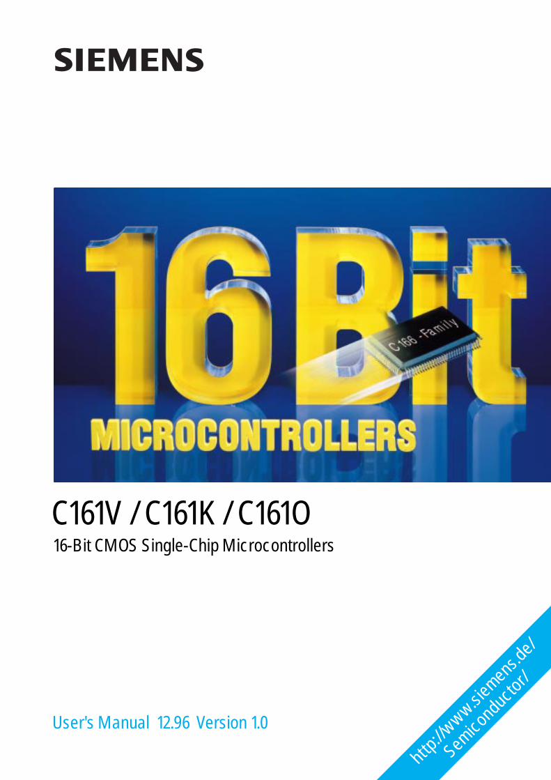
C161V / C161K / C161O16-Bit CMOS Single-Chip Microcontrollers
http://w
ww.siemens.d
e/
Semiconductor/
Edition 12.96This edition was realized using the software system FrameMaker.Published by Siemens AG,Bereich Halbleiter, Marketing-Kommunikation, Balanstraße 73,81541 München© Siemens AG 1996.All Rights Reserved.Attention please!As far as patents or other rights of third par-ties are concerned, liability is only assumed for components, not for applications, pro-cesses and circuits implemented within com-ponents or assemblies.The information describes the type of compo-nent and shall not be considered as assured characteristics.Terms of delivery and rights to change design reserved.For questions on technology, delivery and prices please contact the Semiconductor Group Offices in Germany or the Siemens Companies and Representatives worldwide (see address list).Due to technical requirements components may contain dangerous substances. For in-formation on the types in question please contact your nearest Siemens Office, Semi-conductor Group.Siemens AG is an approved CECC manufac-turer.PackingPlease use the recycling operators known to you. We can also help you – get in touch with your nearest sales office. By agreement we will take packing material back, if it is sorted. You must bear the costs of transport. For packing material that is returned to us un-sorted or which we are not obliged to accept, we shall have to invoice you for any costs in-curred.Components used in life-support devices or systems must be expressly authorized for such purpose!Critical components1 of the Semiconductor Group of Siemens AG, may only be used in life-support devices or systems2 with the ex-press written approval of the Semiconductor Group of Siemens AG.1 A critical component is a component used
in a life-support device or system whose failure can reasonably be expected to cause the failure of that life-support de-vice or system, or to affect its safety or ef-fectiveness of that device or system.
2 Life support devices or systems are in-tended (a) to be implanted in the human body, or (b) to support and/or maintain and sustain human life. If they fail, it is reasonable to assume that the health of the user may be endangered.

C161V / C161K / C161ORevision History: Original Version 1.0 (12.96)
Previous Version: –
Page(in previous version)
Page(in current version)
Subjects (major changes since last revision)
1996 Contents / C161
Table of Contents Page
1 Introduction . . . . . . . . . . . . . . . . . . . . . . . . . . . . . . . . . . . . . . . . . . . . . . . . 1-11.1 The Members of the 16-bit Microcontroller Family . . . . . . . . . . . . . . . . . . . . 1-11.2 Summary of Basic Features . . . . . . . . . . . . . . . . . . . . . . . . . . . . . . . . . . . . . 1-31.3 Abbreviations . . . . . . . . . . . . . . . . . . . . . . . . . . . . . . . . . . . . . . . . . . . . . . . . 1-6
2 Architectural Overview . . . . . . . . . . . . . . . . . . . . . . . . . . . . . . . . . . . . . . . 2-12.1 Basic CPU Concepts and Optimizations . . . . . . . . . . . . . . . . . . . . . . . . . . . 2-22.1.1 High Instruction Bandwidth / Fast Execution . . . . . . . . . . . . . . . . . . . . . . . . 2-32.1.2 Programmable Multiple Priority Interrupt System . . . . . . . . . . . . . . . . . . . . . 2-62.2 The On-chip System Resources . . . . . . . . . . . . . . . . . . . . . . . . . . . . . . . . . 2-72.3 The On-chip Peripheral Blocks . . . . . . . . . . . . . . . . . . . . . . . . . . . . . . . . . 2-112.4 Protected Bits . . . . . . . . . . . . . . . . . . . . . . . . . . . . . . . . . . . . . . . . . . . . . . . 2-15
3 Memory Organization . . . . . . . . . . . . . . . . . . . . . . . . . . . . . . . . . . . . . . . . 3-13.1 Internal ROM . . . . . . . . . . . . . . . . . . . . . . . . . . . . . . . . . . . . . . . . . . . . . . . . 3-33.2 Internal RAM and SFR Area . . . . . . . . . . . . . . . . . . . . . . . . . . . . . . . . . . . . 3-43.3 External Memory Space . . . . . . . . . . . . . . . . . . . . . . . . . . . . . . . . . . . . . . . . 3-93.4 Crossing Memory Boundaries . . . . . . . . . . . . . . . . . . . . . . . . . . . . . . . . . . 3-10
4 The Central Processing Unit (CPU) . . . . . . . . . . . . . . . . . . . . . . . . . . . . . 4-14.1 Instruction Pipelining . . . . . . . . . . . . . . . . . . . . . . . . . . . . . . . . . . . . . . . . . . 4-34.1.1 Particular Pipeline Effects . . . . . . . . . . . . . . . . . . . . . . . . . . . . . . . . . . . . . . 4-64.2 Bit-Handling and Bit-Protection . . . . . . . . . . . . . . . . . . . . . . . . . . . . . . . . . . 4-94.3 Instruction State Times . . . . . . . . . . . . . . . . . . . . . . . . . . . . . . . . . . . . . . . 4-104.4 CPU Special Function Registers . . . . . . . . . . . . . . . . . . . . . . . . . . . . . . . . 4-11
5 Interrupt and Trap Functions . . . . . . . . . . . . . . . . . . . . . . . . . . . . . . . . . . 5-15.1 Interrupt System Structure . . . . . . . . . . . . . . . . . . . . . . . . . . . . . . . . . . . . . . 5-25.1.1 Interrupt Control Registers . . . . . . . . . . . . . . . . . . . . . . . . . . . . . . . . . . . . . . 5-55.2 Operation of the PEC Channels . . . . . . . . . . . . . . . . . . . . . . . . . . . . . . . . . 5-105.3 Prioritization of Interrupt and PEC Service Requests . . . . . . . . . . . . . . . . 5-135.4 Saving the Status during Interrupt Service . . . . . . . . . . . . . . . . . . . . . . . . 5-145.5 Interrupt Response Times . . . . . . . . . . . . . . . . . . . . . . . . . . . . . . . . . . . . . 5-165.5.1 PEC Response Times . . . . . . . . . . . . . . . . . . . . . . . . . . . . . . . . . . . . . . . . 5-185.6 External Interrupts . . . . . . . . . . . . . . . . . . . . . . . . . . . . . . . . . . . . . . . . . . . 5-205.7 Trap Functions . . . . . . . . . . . . . . . . . . . . . . . . . . . . . . . . . . . . . . . . . . . . . . 5-23
6 Parallel Ports . . . . . . . . . . . . . . . . . . . . . . . . . . . . . . . . . . . . . . . . . . . . . . . 6-16.1 PORT0 . . . . . . . . . . . . . . . . . . . . . . . . . . . . . . . . . . . . . . . . . . . . . . . . . . . . . 6-46.1.1 Alternate Functions of PORT0 . . . . . . . . . . . . . . . . . . . . . . . . . . . . . . . . . . . 6-56.2 PORT1 . . . . . . . . . . . . . . . . . . . . . . . . . . . . . . . . . . . . . . . . . . . . . . . . . . . . . 6-76.2.1 Alternate Functions of PORT1 . . . . . . . . . . . . . . . . . . . . . . . . . . . . . . . . . . . 6-86.3 Port 2 . . . . . . . . . . . . . . . . . . . . . . . . . . . . . . . . . . . . . . . . . . . . . . . . . . . . . 6-106.3.1 Alternate Functions of Port 2 . . . . . . . . . . . . . . . . . . . . . . . . . . . . . . . . . . . 6-11
Semiconductor Group I-1

1996 Contents / C161
Table of Contents Page
6.4 Port 3 . . . . . . . . . . . . . . . . . . . . . . . . . . . . . . . . . . . . . . . . . . . . . . . . . . . . . 6-136.4.1 Alternate Functions of Port 3 . . . . . . . . . . . . . . . . . . . . . . . . . . . . . . . . . . . 6-146.5 Port 4 . . . . . . . . . . . . . . . . . . . . . . . . . . . . . . . . . . . . . . . . . . . . . . . . . . . . . 6-186.5.1 Alternate Functions of Port 4 . . . . . . . . . . . . . . . . . . . . . . . . . . . . . . . . . . . 6-186.6 Port 5 . . . . . . . . . . . . . . . . . . . . . . . . . . . . . . . . . . . . . . . . . . . . . . . . . . . . . 6-216.6.1 Alternate Functions of Port 5 . . . . . . . . . . . . . . . . . . . . . . . . . . . . . . . . . . . 6-216.7 Port 6 . . . . . . . . . . . . . . . . . . . . . . . . . . . . . . . . . . . . . . . . . . . . . . . . . . . . . 6-236.7.1 Alternate Functions of Port 6 . . . . . . . . . . . . . . . . . . . . . . . . . . . . . . . . . . . 6-24
7 Dedicated Pins . . . . . . . . . . . . . . . . . . . . . . . . . . . . . . . . . . . . . . . . . . . . . . 7-1
8 The External Bus Interface . . . . . . . . . . . . . . . . . . . . . . . . . . . . . . . . . . . . 8-18.1 External Bus Modes . . . . . . . . . . . . . . . . . . . . . . . . . . . . . . . . . . . . . . . . . . . 8-28.2 Programmable Bus Characteristics . . . . . . . . . . . . . . . . . . . . . . . . . . . . . . 8-108.3 Controlling the External Bus Controller . . . . . . . . . . . . . . . . . . . . . . . . . . . 8-158.4 EBC Idle State . . . . . . . . . . . . . . . . . . . . . . . . . . . . . . . . . . . . . . . . . . . . . . 8-238.5 The XBUS Interface . . . . . . . . . . . . . . . . . . . . . . . . . . . . . . . . . . . . . . . . . . 8-24
9 The General Purpose Timer Units . . . . . . . . . . . . . . . . . . . . . . . . . . . . . . 9-19.1 Timer Block GPT1 . . . . . . . . . . . . . . . . . . . . . . . . . . . . . . . . . . . . . . . . . . . . 9-19.1.1 GPT1 Core Timer T3 . . . . . . . . . . . . . . . . . . . . . . . . . . . . . . . . . . . . . . . . . . 9-39.1.2 GPT1 Auxiliary Timers T2 and T4 . . . . . . . . . . . . . . . . . . . . . . . . . . . . . . . . 9-89.1.3 Interrupt Control for GPT1 Timers . . . . . . . . . . . . . . . . . . . . . . . . . . . . . . . 9-159.2 Timer Block GPT2 . . . . . . . . . . . . . . . . . . . . . . . . . . . . . . . . . . . . . . . . . . . 9-169.2.1 GPT2 Core Timer T6 . . . . . . . . . . . . . . . . . . . . . . . . . . . . . . . . . . . . . . . . . 9-189.2.2 GPT2 Auxiliary Timer T5 . . . . . . . . . . . . . . . . . . . . . . . . . . . . . . . . . . . . . . 9-209.2.3 Interrupt Control for GPT2 Timers and CAPREL . . . . . . . . . . . . . . . . . . . . 9-26
10 The Asynchronous/Synchr. Serial Interface . . . . . . . . . . . . . . . . . . . . . 10-110.1 Asynchronous Operation . . . . . . . . . . . . . . . . . . . . . . . . . . . . . . . . . . . . . . 10-410.2 Synchronous Operation . . . . . . . . . . . . . . . . . . . . . . . . . . . . . . . . . . . . . . . 10-810.3 Hardware Error Detection Capabilities . . . . . . . . . . . . . . . . . . . . . . . . . . . 10-1010.4 ASC0 Baud Rate Generation . . . . . . . . . . . . . . . . . . . . . . . . . . . . . . . . . . 10-1010.5 ASC0 Interrupt Control . . . . . . . . . . . . . . . . . . . . . . . . . . . . . . . . . . . . . . . 10-12
11 The High-Speed Synchronous Serial Interface . . . . . . . . . . . . . . . . . . . 11-111.1 Full-Duplex Operation . . . . . . . . . . . . . . . . . . . . . . . . . . . . . . . . . . . . . . . . 11-611.2 Half Duplex Operation . . . . . . . . . . . . . . . . . . . . . . . . . . . . . . . . . . . . . . . . 11-811.3 Baud Rate Generation . . . . . . . . . . . . . . . . . . . . . . . . . . . . . . . . . . . . . . . 11-1011.4 Error Detection Mechanisms . . . . . . . . . . . . . . . . . . . . . . . . . . . . . . . . . . 11-1211.5 SSC Interrupt Control . . . . . . . . . . . . . . . . . . . . . . . . . . . . . . . . . . . . . . . . 11-14
12 The Watchdog Timer (WDT) . . . . . . . . . . . . . . . . . . . . . . . . . . . . . . . . . . 12-1
13 The Bootstrap Loader . . . . . . . . . . . . . . . . . . . . . . . . . . . . . . . . . . . . . . . 13-1
Semiconductor Group I-2

1996 Contents / C161
Table of Contents Page
14 System Reset . . . . . . . . . . . . . . . . . . . . . . . . . . . . . . . . . . . . . . . . . . . . . . 14-1
15 Power Reduction Modes . . . . . . . . . . . . . . . . . . . . . . . . . . . . . . . . . . . . . 15-115.1 Idle Mode . . . . . . . . . . . . . . . . . . . . . . . . . . . . . . . . . . . . . . . . . . . . . . . . . . 15-115.2 Power Down Mode . . . . . . . . . . . . . . . . . . . . . . . . . . . . . . . . . . . . . . . . . . . 15-315.3 Status of Output Pins during Idle and Power Down Mode . . . . . . . . . . . . . 15-4
16 System Programming . . . . . . . . . . . . . . . . . . . . . . . . . . . . . . . . . . . . . . . 16-116.1 Stack Operations . . . . . . . . . . . . . . . . . . . . . . . . . . . . . . . . . . . . . . . . . . . . 16-416.2 Register Banking . . . . . . . . . . . . . . . . . . . . . . . . . . . . . . . . . . . . . . . . . . . . 16-816.3 Procedure Call Entry and Exit . . . . . . . . . . . . . . . . . . . . . . . . . . . . . . . . . . 16-816.4 Table Searching . . . . . . . . . . . . . . . . . . . . . . . . . . . . . . . . . . . . . . . . . . . . 16-1116.5 Peripheral Control and Interface . . . . . . . . . . . . . . . . . . . . . . . . . . . . . . . 16-1116.6 Floating Point Support . . . . . . . . . . . . . . . . . . . . . . . . . . . . . . . . . . . . . . . 16-1216.7 Trap/Interrupt Entry and Exit . . . . . . . . . . . . . . . . . . . . . . . . . . . . . . . . . . 16-1216.8 Unseparable Instruction Sequences . . . . . . . . . . . . . . . . . . . . . . . . . . . . 16-1216.9 Overriding the DPP Addressing Mechanism . . . . . . . . . . . . . . . . . . . . . . 16-1316.10 Handling the Internal ROM . . . . . . . . . . . . . . . . . . . . . . . . . . . . . . . . . . . 16-1416.11 Pits, Traps and Mines . . . . . . . . . . . . . . . . . . . . . . . . . . . . . . . . . . . . . . . 16-15
17 The Register Set . . . . . . . . . . . . . . . . . . . . . . . . . . . . . . . . . . . . . . . . . . . . 17-117.1 CPU General Purpose Registers (GPRs) . . . . . . . . . . . . . . . . . . . . . . . . . 17-217.2 Special Function Registers ordered by Name . . . . . . . . . . . . . . . . . . . . . . 17-417.3 Registers ordered by Address . . . . . . . . . . . . . . . . . . . . . . . . . . . . . . . . . . 17-817.4 Special Notes . . . . . . . . . . . . . . . . . . . . . . . . . . . . . . . . . . . . . . . . . . . . . . 17-12
18 Instruction Set Summary . . . . . . . . . . . . . . . . . . . . . . . . . . . . . . . . . . . . . 18-1
19 Device Specification . . . . . . . . . . . . . . . . . . . . . . . . . . . . . . . . . . . . . . . . 19-1
20 Keyword Index . . . . . . . . . . . . . . . . . . . . . . . . . . . . . . . . . . . . . . . . . . . . . 20-1
Semiconductor Group I-3

10Jul97@15:19h Introduction / C161
1 Introduction
The rapidly growing area of embedded control applications is representing one of the most time-critical operating environments for today’s microcontrollers. Complex control algorithms have to beprocessed based on a large number of digital as well as analog input signals, and the appropriateoutput signals must be generated within a defined maximum response time. Embedded controlapplications also are often sensitive to board space, power consumption, and overall system cost.
Embedded control applications therefore require microcontrollers, which...
• offer a high level of system integration• eliminate the need for additional peripheral devices and the associated software overhead• provide system security and fail-safe mechanisms.
With the increasing complexity of embedded control applications, a significant increase in CPUperformance and peripheral functionality over conventional 8-bit controllers is required frommicrocontrollers for high-end embedded control systems. In order to achieve this high performancegoal Siemens has decided to develop its family of 16-bit CMOS microcontrollers without theconstraints of backward compatibility.
Of course the architecture of the 16-bit microcontroller family pursues successfull hardware andsoftware concepts, which have been established in Siemens's popular 8-bit controller families.
1.1 The Members of the 16-bit Microcontroller Family
The microcontrollers of the Siemens 16-bit family have been designed to meet the highperformance requirements of real-time embedded control applications. The architecture of thisfamily has been optimized for high instruction throughput and minimum response time to externalstimuli (interrupts). Intelligent peripheral subsystems have been integrated to reduce the need forCPU intervention to a minimum extent. This also minimizes the need for communication via theexternal bus interface. The high flexibility of this architecture allows to serve the diverse and varyingneeds of different application areas such as automotive, industrial control, or data communications.
The core of the 16-bit family has been developped with a modular family concept in mind. All familymembers execute an efficient control-optimized instruction set (additional instructions for membersof the second generation). This allows an easy and quick implementation of new family memberswith different internal memory sizes and technologies, different sets of on-chip peripherals and/ordifferent numbers of IO pins.
The XBUS concept opens a straight forward path for the integration of application specificperipheral modules in addition to the standard on-chip peripherals in order to build applicationspecific derivatives.
As programs for embedded control applications become larger, high level languages are favouredby programmers, because high level language programs are easier to write, to debug and tomaintain.
Semiconductor Group 1-1

10Jul97@15:19h Introduction / C161
The 80C166-type microcontrollers were the first generation of the 16-bit controller family. Thesedevices have established the C166 architecture.
The C165-type and C167-type devices are members of the second generation of this family. Thissecond generation is even more powerful due to additional instructions for HLL support, anincreased address space, increased internal RAM and highly efficient management of variousresources on the external bus.
Utilizing integration to design efficient systems may require the integration of application specificperipherals to boost system performance, while minimizing the part count. These efforts aresupported by the so-called XBUS, defined for the Siemens 16-bit microcontrollers (secondgeneration). This XBUS is an internal representation of the external bus interface that opens andsimplifies the integration of peripherals by standardizing the required interface. One representativetaking advantage of this technology is the integrated CAN module that is offered by some devices.
The C165-type devices are reduced versions of the C167 which provide a smaller package andreduced power consumption at the expense of the A/D converter, the CAPCOM units and the PWMmodule. The C161 derivatives are especially suited for cost sensitive applications.
A variety of different versions is provided which offer mask-programmable ROM, Flash memory orno non-volatile memory at all. Also there are devices with specific functional units.
The devices may be offered in different packages, temperature ranges and speed classes.
More standard and application-specific derivatives are planned and in development.
Information about specific versions and derivatives will be made available with the devicesthemselves. Contact your Siemens representative for up-to-date material.
Note: As the architecture and the basic features (ie. CPU core and built in peripherals) are identicalfor most of the currently offered versions of the C161, the descriptions within this manual thatrefer to the “C161” also apply to the other variations, unless otherwise noted.Especially those parts which refer exclusively to a single derivative are marked.
Semiconductor Group 1-2
10Jul97@15:19h Introduction / C161
1.2 Summary of Basic Features
The C161 is a cost effective representative of the Siemens family of full featured 16-bit single-chipCMOS microcontrollers. It combines high CPU performance (up to 8 million instructions per second)with high peripheral functionality.Several key features contribute to the high performance of the C161.
High Performance 16-Bit CPU With Four-Stage Pipeline
• 125 ns minimum instruction cycle time, with most instructions executed in 1 cycle• 625 ns multiplication (16-bit *16-bit), 1.25 µs division (32-bit/16-bit)• Multiple high bandwidth internal data buses• Register based design with multiple variable register banks• Single cycle context switching support• 4 MBytes linear address space for code and data (von Neumann architecture)• System stack cache support with automatic stack overflow/underflow detection
Control Oriented Instruction Set with High Efficiency
• Bit, byte, and word data types• Flexible and efficient addressing modes for high code density• Enhanced boolean bit manipulation with direct addressability of 4 Kbits
for peripheral control and user defined flags• Hardware traps to identify exception conditions during runtime• HLL support for semaphore operations and efficient data access
Integrated On-chip Memory
• Internal RAM for variables, register banks, system stack and code(2 KByte on the C161O, 1 KByte on the C161V C161K)
• Internal Mask ROM, OTP or Flash memory (not for romless devices)
External Bus Interface
• Multiplexed or demultiplexed bus configurations (MUX only on C161V)• Segmentation capability and chip select signal generation (not on the C161V)• 8-bit or 16-bit data bus• Bus cycle characteristics selectable for five programmable address areas
16-Priority-Level Interrupt System
• 20/14 interrupt nodes (C161O/C161V/K) with separate interrupt vectors• 315/625 ns typical/maximum interrupt latency in case of internal program execution• Fast external interrupts
Semiconductor Group 1-3
10Jul97@15:19h Introduction / C161
8-Channel Peripheral Event Controller (PEC)
• Interrupt driven single cycle data transfer• Transfer count option (standard CPU interrupt after a programmable
number of PEC transfers)• Eliminates overhead of saving and restoring system state for interrupt requests
Intelligent On-chip Peripheral Subsystems
• Multifunctional General Purpose Timer UnitsGPT1: three 16-bit timers/ counters, 500 ns maximum resolutionGPT2: two 16-bit timers/counters, 250 ns maximum resolution (C161O only)
• Asynchronous/Synchronous Serial Channel (USART)with baud rate generator, parity, framing, and overrun error detection
• High Speed Synchronous Serial Channelprogrammable data length and shift direction
• Watchdog Timer with programmable time intervals• Bootstrap Loader for flexible system initialization (not in the C161V)
63 IO Lines With Individual Bit Addressability
• Tri-stated in input mode• Push/pull or open drain output mode
Different Temperature Ranges
• 0 to +70 °C, –40 to +85 °C
Siemens CMOS Process
• Low Power CMOS Technology, including power saving Idle and Power Down modes
80-Pin Plastic Quad Flat Pack (PQFP) Package
• P-MQFP, 14*14 mm body, 0.65 mm (25.6 mil) lead spacing, surface mount technology
Semiconductor Group 1-4

10Jul97@15:19h Introduction / C161
Device Cross-Reference
The table below describes the differences between the three derivatives described in this datasheet. This table provides an overview on the capabilities of each derivative for a quick comparison.
Complete Development Support
A variety of software and hardware development tools for the Siemens family of 16-bitmicrocontrollers is available from experienced international tool suppliers. The high quality andreliability of these tools is already proven in many applications and by many users. The toolenvironment for the Siemens 16-bit microcontrollers includes the following tools:
• Compilers (C, MODULA2, FORTH)• Macro-Assemblers, Linkers, Locaters, Library Managers, Format-Converters• Architectural Simulators• HLL debuggers• Real-Time operating systems• VHDL chip models• In-Circuit Emulators (based on bondout or standard chips)• Plug-In emulators• Emulation and Clip-Over adapters, production sockets• Logic Analyzer disassemblers• Evaluation Boards with monitor programs• Industrial boards (also for CAN, FUZZY, PROFIBUS, FORTH applications)• Network driver software (CAN, PROFIBUS)
Feature C161V C161K C161O
Internal RAM Size (IRAM) 1 KByte 1 KByte 2 KBytes
Chip Select Signals --- 2 4
Bus Modes MUX MUX / Demux MUX / Demux
Power Saving Modes --- yes yes
Fast External Interrupts 4 4 7
General Purpose Timer Unit 1 (GPT1) yes yes yes
Input / Output Functionality of GPT1 --- yes yes
General Purpose Timer Unit 2 (GPT2)with Capture Input (CAPIN) Functionality
--- --- yes
Built-in Bootstrap Loader --- yes yes
Semiconductor Group 1-5

10Jul97@15:19h Introduction / C161
1.3 Abbreviations
The following acronyms and termini are used within this document:
ALE . . . . . . . . . . Address Latch Enable
ALU. . . . . . . . . . Arithmetic and Logic Unit
ASC . . . . . . . . . Asynchronous/synchronous Serial Controller
CISC . . . . . . . . . Complex Instruction Set Computing
CMOS . . . . . . . . Complementary Metal Oxide Silicon
CPU . . . . . . . . . Central Processing Unit
EBC . . . . . . . . . External Bus Controller
ESFR . . . . . . . . Extended Special Function Register
Flash . . . . . . . . . Non-volatile memory that may be electrically erased
GPR . . . . . . . . . General Purpose Register
GPT . . . . . . . . . General Purpose Timer unit
HLL . . . . . . . . . . High Level Language
IO . . . . . . . . . . . Input / Output
OTP . . . . . . . . . One Time Programmable non-volatile Memory
PEC . . . . . . . . . Peripheral Event Controller
PLA . . . . . . . . . . Programmable Logic Array
RAM . . . . . . . . . Random Access Memory
RISC . . . . . . . . . Reduced Instruction Set Computing
ROM . . . . . . . . . Read Only Memory
SFR. . . . . . . . . . Special Function Register
SSC . . . . . . . . . Synchronous Serial Controller
XBUS . . . . . . . . Internal representation of the External Bus
Semiconductor Group 1-6
10Jul97@15:19h Architectural Overview / C161
2 Architectural Overview
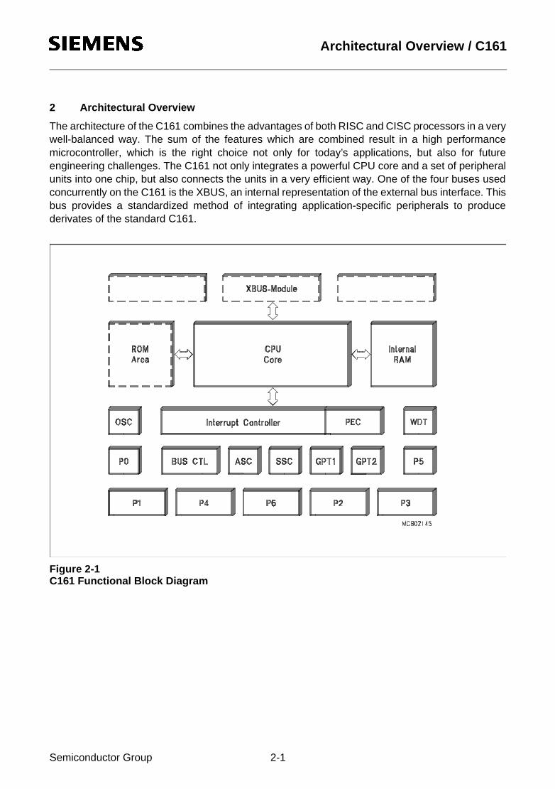
The architecture of the C161 combines the advantages of both RISC and CISC processors in a verywell-balanced way. The sum of the features which are combined result in a high performancemicrocontroller, which is the right choice not only for today’s applications, but also for futureengineering challenges. The C161 not only integrates a powerful CPU core and a set of peripheralunits into one chip, but also connects the units in a very efficient way. One of the four buses usedconcurrently on the C161 is the XBUS, an internal representation of the external bus interface. Thisbus provides a standardized method of integrating application-specific peripherals to producederivates of the standard C161.
Figure 2-1C161 Functional Block Diagram
Semiconductor Group 2-1

10Jul97@15:19h Architectural Overview / C161
2.1 Basic CPU Concepts and Optimizations
The main core of the CPU consists of a 4-stage instruction pipeline, a 16-bit arithmetic and logic unit(ALU) and dedicated SFRs. Additional hardware is provided for a separate multiply and divide unit,a bit-mask generator and a barrel shifter.
Figure 2-2CPU Block Diagram
To meet the demand for greater performance and flexibility, a number of areas has been optimizedin the processor core. Functional blocks in the CPU core are controlled by signals from theinstruction decode logic. These are summarized below, and described in detail in the followingsections:
1) High Instruction Bandwidth / Fast Execution
2) High Function 8-bit and 16-bit Arithmetic and Logic Unit
3) Extended Bit Processing and Peripheral Control
4) High Performance Branch-, Call-, and Loop Processing
5) Consistent and Optimized Instruction Formats
6) Programmable Multiple Priority Interrupt Structure
Semiconductor Group 2-2
10Jul97@15:19h Architectural Overview / C161
High Instruction Bandwidth / Fast Execution
Based on the hardware provisions, most of the C161’s instructions can be exected in just onemachine cycle, which requires 125 ns at 16 MHz CPU clock. For example, shift and rotateinstructions are always processed within one machine cycle, independent of the number of bits tobe shifted.
Branch-, multiply- and divide instructions normally take more than one machine cycle. Theseinstructions, however, have also been optimized. For example, branch instructions only require anadditional machine cycle, when a branch is taken, and most branches taken in loops require noadditional machine cycles at all, due to the so-called ‘Jump Cache’.A 32-bit / 16-bit division takes 1µs, a 16-bit * 16-bit multiplication takes 0.625 µs.
The instruction cycle time has been dramatically reduced through the use of instruction pipelining.This technique allows the core CPU to process portions of multiple sequential instruction stages inparallel. The following four stage pipeline provides the optimum balancing for the CPU core:
FETCH: In this stage, an instruction is fetched from the internal ROM or RAM or from the externalmemory, based on the current IP value.
DECODE: In this stage, the previously fetched instruction is decoded and the required operandsare fetched.
EXECUTE: In this stage, the specified operation is performed on the previously fetched operands.
WRITE BACK: In this stage, the result is written to the specified location.
If this technique were not used, each instruction would require four machine cycles. This increasedperformance allows a greater number of tasks and interrupts to be processed.
Instruction Decoder
Instruction decoding is primarily generated from PLA outputs based on the selected opcode. Nomicrocode is used and each pipeline stage receives control signals staged in control registers fromthe decode stage PLAs. Pipeline holds are primarily caused by wait states for external memoryaccesses and cause the holding of signals in the control registers. Multiple-cycle instructions areperformed through instruction injection and simple internal state machines which modify requiredcontrol signals.
High Function 8-bit and 16-bit Arithmetic and Logic Unit
All standard arithmetic and logical operations are performed in a 16-bit ALU. In addition, for byteoperations, signals are provided from bits six and seven of the ALU result to correctly set thecondition flags. Multiple precision arithmetic is provided through a 'CARRY-IN' signal to the ALUfrom previously calculated portions of the desired operation. Most internal execution blocks havebeen optimized to perform operations on either 8-bit or 16-bit quantities. Once the pipeline has beenfilled, one instruction is completed per machine cycle, except for multiply and divide. An advancedBooth algorithm has been incorporated to allow four bits to be multiplied and two bits to be dividedper machine cycle. Thus, these operations use two coupled 16-bit registers, MDL and MDH, andrequire four and nine machine cycles, respectively, to perform a 16-bit by 16-bit (or 32-bit by 16-bit)calculation plus one machine cycle to setup and adjust the operands and the result. Even these
Semiconductor Group 2-3

10Jul97@15:19h Architectural Overview / C161
longer multiply and divide instructions can be interrupted during their execution to allow for very fastinterrupt response. Instructions have also been provided to allow byte packing in memory whileproviding sign extension of bytes for word wide arithmetic operations. The internal bus structurealso allows transfers of bytes or words to or from peripherals based on the peripheral requirements.
A set of consistent flags is automatically updated in the PSW after each arithmetic, logical, shift, ormovement operation. These flags allow branching on specific conditions. Support for both signedand unsigned arithmetic is provided through user-specifiable branch tests. These flags are alsopreserved automatically by the CPU upon entry into an interrupt or trap routine.All targets for branch calculations are also computed in the central ALU.
A 16-bit barrel shifter provides multiple bit shifts in a single cycle. Rotates and arithmetic shifts arealso supported.
Extended Bit Processing and Peripheral Control
A large number of instructions has been dedicated to bit processing. These instructions provideefficient control and testing of peripherals while enhancing data manipulation. Unlike othermicrocontrollers, these instructions provide direct access to two operands in the bit-addressablespace without requiring to move them into temporary flags.
The same logical instructions available for words and bytes are also supported for bits. This allowsthe user to compare and modify a control bit for a peripheral in one instruction. Multiple bit shiftinstructions have been included to avoid long instruction streams of single bit shift operations.These are also performed in a single machine cycle.
In addition, bit field instructions have been provided, which allow the modification of multiple bitsfrom one operand in a single instruction.
High Performance Branch-, Call-, and Loop Processing
Due to the high percentage of branching in controller applications, branch instructions have beenoptimized to require one extra machine cycle only when a branch is taken. This is implemented byprecalculating the target address while decoding the instruction. To decrease loop executionoverhead, three enhancements have been provided:
• The first solution provides single cycle branch execution after the first iteration of a loop. Thus, onlyone machine cycle is lost during the execution of the entire loop. In loops which fall through uponcompletion, no machine cycles are lost when exiting the loop. No special instructions are requiredto perform loops, and loops are automatically detected during execution of branch instructions.
• The second loop enhancement allows the detection of the end of a table and avoids the use of twocompare instructions embedded in loops. One simply places the lowest negative number at the endof the specific table, and specifies branching if neither this value nor the compared value have beenfound. Otherwise the loop is terminated if either condition has been met. The terminating conditioncan then be tested.
• The third loop enhancement provides a more flexible solution than the Decrement and Skip onZero instruction which is found in other microcontrollers. Through the use of Compare andIncrement or Decrement instructions, the user can make comparisons to any value. This allows loopcounters to cover any range. This is particularly advantageous in table searching.
Semiconductor Group 2-4

10Jul97@15:19h Architectural Overview / C161
Saving of system state is automatically performed on the internal system stack avoiding the use ofinstructions to preserve state upon entry and exit of interrupt or trap routines. Call instructions pushthe value of the IP on the system stack, and require the same execution time as branch instructions.
Instructions have also been provided to support indirect branch and call instructions. This supportsimplementation of multiple CASE statement branching in assembler macros and high levellanguages.
Consistent and Optimized Instruction Formats
To obtain optimum performance in a pipelined design, an instruction set has been designed whichincorporates concepts from Reduced Instruction Set Computing (RISC). These concepts primarilyallow fast decoding of the instructions and operands while reducing pipeline holds. These concepts,however, do not preclude the use of complex instructions, which are required by microcontrollerusers. The following goals were used to design the instruction set:
1) Provide powerful instructions to perform operations which currently require sequences of instructions and are frequently used. Avoid transfer into and out of temporary registers such as accumulators and carry bits. Perform tasks in parallel such as saving state upon entry into interrupt routines or subroutines.
2) Avoid complex encoding schemes by placing operands in consistent fields for each instruc-tion. Also avoid complex addressing modes which are not frequently used. This decreases the instruction decode time while also simplifying the development of compilers and assem-blers.
3) Provide most frequently used instructions with one-word instruction formats. All other instruc-tions are placed into two-word formats. This allows all instructions to be placed on word boundaries, which alleviates the need for complex alignment hardware. It also has the bene-fit of increasing the range for relative branching instructions.
The high performance offered by the hardware implementation of the CPU can efficiently be utilizedby a programmer via the highly functional C161 instruction set which includes the followinginstruction classes:
• Arithmetic Instructions• Logical Instructions• Boolean Bit Manipulation Instructions• Compare and Loop Control Instructions• Shift and Rotate Instructions• Prioritize Instruction• Data Movement Instructions• System Stack Instructions• Jump and Call Instructions• Return Instructions• System Control Instructions• Miscellaneous Instructions
Possible operand types are bits, bytes and words. Specific instruction support the conversion(extension) of bytes to words. A variety of direct, indirect or immediate addressing modes areprovided to specify the required operands.
Semiconductor Group 2-5
10Jul97@15:19h Architectural Overview / C161
Programmable Multiple Priority Interrupt System
The following enhancements have been included to allow processing of a large number of interruptsources:
1) Peripheral Event Controller (PEC): This processor is used to off-load many interrupt requests from the CPU. It avoids the overhead of entering and exiting interrupt or trap routines by per-forming single-cycle interrupt-driven byte or word data transfers between any two locations in segment 0 with an optional increment of either the PEC source or the destination pointer. Just one cycle is ’stolen’ from the current CPU activity to perform a PEC service.
2) Multiple Priority Interrupt Controller: This controller allows all interrupts to be placed at any specified priority. Interrupts may also be grouped, which provides the user with the ability to prevent similar priority tasks from interrupting each other. For each of the possible interrupt sources there is a separate control register, which contains an interrupt request flag, an inter-rupt enable flag and an interrupt priority bitfield. Once having been accepted by the CPU, an interrupt service can only be interrupted by a higher prioritized service request. For standard interrupt processing, each of the possible interrupt sources has a dedicated vector location.
3) Multiple Register Banks: This feature allows the user to specify up to sixteen general pur-pose registers located anywhere in the internal RAM. A single one-machine-cycle instruction allows to switch register banks from one task to another.
4) Interruptable Multiple Cycle Instructions: Reduced interrupt latency is provided by allowing multiple-cycle instructions (multiply, divide) to be interruptable.
With an interrupt response time within a range from just 315 ns to 625 ns (in case of internalprogram execution), the C161 is capable of reacting very fast on non-deterministic events.
Its fast external interrupt inputs are sampled every 65 ns and allow to recognize even very shortexternal signals.
The C161 also provides an excellent mechanism to identify and to process exceptions or errorconditions that arise during run-time, so called ’Hardware Traps’. Hardware traps cause animmediate non-maskable system reaction which is similiar to a standard interrupt service(branching to a dedicated vector table location). The occurrence of a hardware trap is additionallysignified by an individual bit in the trap flag register (TFR). Except for another higher prioritized trapservice being in progress, a hardware trap will interrupt any current program execution. In turn,hardware trap services can normally not be interrupted by standard or PEC interrupts.
Software interrupts are supported by means of the ’TRAP’ instruction in combination with anindividual trap (interrupt) number.
Semiconductor Group 2-6

10Jul97@15:19h Architectural Overview / C161
2.2 The On-chip System Resources
The C161 controllers provide a number of powerful system resources designed around the CPU.The combination of CPU and these resources results in the high performance of the members ofthis controller family.
Peripheral Event Controller (PEC) and Interrupt Control
The Peripheral Event Controller allows to respond to an interrupt request with a single data transfer(word or byte) which only consumes one instruction cycle and does not require to save and restorethe machine status. Each interrupt source is prioritized every machine cycle in the interrupt controlblock. If PEC service is selected, a PEC transfer is started. If CPU interrupt service is requested, thecurrent CPU priority level stored in the PSW register is tested to determine whether a higher priorityinterrupt is currently being serviced. When an interrupt is acknowledged, the current state of themachine is saved on the internal system stack and the CPU branches to the system specific vectorfor the peripheral.
The PEC contains a set of SFRs which store the count value and control bits for eight data transferchannels. In addition, the PEC uses a dedicated area of RAM which contains the source anddestination addresses. The PEC is controlled similar to any other peripheral through SFRscontaining the desired configuration of each channel.
An individual PEC transfer counter is implicitly decremented for each PEC service except formingin the continuous transfer mode. When this counter reaches zero, a standard interrupt is performedto the vector location related to the corresponding source. PEC services are very well suited, forexample, to move register contents to/from a memory table. The C161 has 8 PEC channels eachof which offers such fast interrupt-driven data transfer capabilities.
Memory Areas
The memory space of the C161 is configured in a Von Neumann architecture which means thatcode memory, data memory, registers and IO ports are organized within the same linear addressspace which covers up to 16 MBytes. The entire memory space can be accessed bytewise orwordwise. Particular portions of the on-chip memory have additionally been made directly bitaddressable.
A 16-bit wide internal RAM (IRAM) provides fast access to General Purpose Registers (GPRs),user data (variables) and system stack. The internal RAM may also be used for code. A uniquedecoding scheme provides flexible user register banks in the internal memory while optimizing theremaining RAM for user data.
The size of the internal RAM is ...... 2 KByte for the C161O,... 1 KByte for the C161V and the C161K.
The CPU disposes of an actual register context consisting of up to 16 wordwide and/or bytewideGPRs, which are physically located within the on-chip RAM area. A Context Pointer (CP) registerdetermines the base address of the active register bank to be accessed by the CPU at a time. Thenumber of register banks is only restricted by the available internal RAM space. For easy parameterpassing, a register bank may overlap others.
Semiconductor Group 2-7
10Jul97@15:19h Architectural Overview / C161
A system stack of up to 1024 words is provided as a storage for temporary data. The system stackis also located within the on-chip RAM area, and it is accessed by the CPU via the stack pointer (SP)register. Two separate SFRs, STKOV and STKUN, are implicitly compared against the stackpointer value upon each stack access for the detection of a stack overflow or underflow.
Hardware detection of the selected memory space is placed at the internal memory decoders andallows the user to specify any address directly or indirectly and obtain the desired data without usingtemporary registers or special instructions.
An optional internal ROM provides for both code and constant data storage. This memory area isconnected to the CPU via a 32-bit-wide bus. Thus, an entire double-word instruction can be fetchedin just one machine cycle. Program execution from the on-chip ROM is the fastest of all possiblealternatives.
For Special Function Registers 1024 Bytes of the address space are reserved. The standardSpecial Function Register area (SFR) uses 512 bytes, while the Extended Special FunctionRegister area (ESFR) uses the other 512 bytes. (E)SFRs are wordwide registers which are used forcontrolling and monitoring functions of the different on-chip units. Unused (E)SFR addresses arereserved for future members of the C161 family with enhanced functionality.
External Bus Interface
In order to meet the needs of designs where more memory is required than is provided on chip, upto 4 MBytes of external RAM and/or ROM can be connected to the microcontroller via its externalbus interface. The integrated External Bus Controller (EBC) allows to access external memory and/or peripheral resources in a very flexible way. For up to five address areas the bus mode(multiplexed / demultiplexed), the data bus width (8-bit / 16-bit) and even the length of a bus cycle(waitstates, signal delays) can be selected independently. This allows to access a variety ofmemory and peripheral components directly and with maximum efficiency. If the device does notrun in Single Chip Mode, where no external memory is required, the EBC can control externalaccesses in one of the following four different external access modes:
16-/18-/20-/22-bit Addresses, 16-bit Data, Demultiplexed 16-/18-/20-/22-bit Addresses, 8-bit Data, Demultiplexed 16-/18-/20-/22-bit Addresses, 16-bit Data, Multiplexed 16-/18-/20-/22-bit Addresses, 8-bit Data, Multiplexed
The demultiplexed bus modes use PORT1 for addresses and PORT0 for data input/output. Themultiplexed bus modes use PORT0 for both addresses and data input/output. All modes use Port 4for the upper address lines (A16...) if selected.
Important timing characteristics of the external bus interface (waitstates, ALE length and Read/Write Delay) have been made programmable to allow the user the adaption of a wide range ofdifferent types of memories and/or peripherals.
For applications which require less than 64 KBytes of address space, a non-segmented memorymodel can be selected, where all locations can be addressed by 16 bits, and thus Port 4 is notneeded as an output for the upper address bits (A21/A19/A17...A16), as is the case when using thesegmented memory model.
Note: The Demultiplexed bus modes are supported by the C161K and the C161O,not by the C161V.
Semiconductor Group 2-8

10Jul97@15:19h Architectural Overview / C161
The on-chip XBUS is an internal representation of the external bus and allows to access integratedapplication-specific peripherals/modules in the same way as external components. It provides adefined interface for these customized peripherals.
The C161 derivatives have no X-Peripherals implemented.
Clock Generator
The on-chip clock generator provides the C161 with its basic clock signal that controls all activitiesof the controller hardware. Its oscillator can either run with an external crystal and appropriateoscillator circuitry (see also recommendations in chapter „Dedicated Pins“) or it can be driven by anexternal oscillator. The oscillator either directly feeds the external clock signal to the controllerhardware (through buffers, of course) or divides the external clock frequency by 2. This resultinginternal clock signal is also referred to as “CPU clock”. Two separated clock signals are generatedfor the CPU itself and the peripheral part of the chip. While the CPU clock is stopped during the idlemode, the peripheral clock keeps running. Both clocks are switched off, when the power downmode is entered.
Figure 2-3Clock Generation Block Diagram
C161 Clock Generation Modes
1) Prescaler operation. Default configuration after reset.2) Direct drive: the maximum frequency depends on the duty cycle of the external clock signal.
In emulation mode pin P0.15 (P0H.7) is inverted, ie. the configuration ’1XX’ would selectdirect drive in emulation mode.
Reset ConfigurationP0.15-13 (P0H.7-5)
CPU Frequency External Clock Input Range
1 X X fXTAL / 2 1) 2 to 32 MHz
0 X X fXTAL * 1 2) 1 to 16 MHz 2)
Semiconductor Group 2-9

10Jul97@15:19h Architectural Overview / C161
Prescaler Operation
When pins P0.15-13 (P0H.7-5) equal ’001’ (C163) during reset (’1XX’ on the C165) the CPU clockis derived from the internal oscillator (input clock signal) by a 2:1 prescaler.The frequency of fCPU is half the frequency of fXTAL and the high and low time of fCPU (ie. theduration of an individual TCL) is defined by the period of the input clock fXTAL.
The timings listed in the „AC Characteristics“ of the data sheet that refer to TCLs therefore can becalculated using the period of fXTAL for any TCL.
Direct Drive
When pins P0.15-13 (P0H.7-5) equal ’011’ (C163) during reset (’0XX’ on the C165) the clocksystem is directly driven from the internal oscillator with the input clock signal, ie. fOSC = fCPU.
The maximum input clock frequency depends on the clock signal’s duty cycle, because theminimum values for the clock phases (TCLs) must be respected.
Semiconductor Group 2-10
10Jul97@15:19h Architectural Overview / C161
2.3 The On-chip Peripheral Blocks
The C161 family clearly separates peripherals from the core. This structure permits the maximumnumber of operations to be performed in parallel and allows peripherals to be added or deleted fromfamily members without modifications to the core. Each functional block processes dataindependently and communicates information over common buses. Peripherals are controlled bydata written to the respective Special Function Registers (SFRs). These SFRs are located eitherwithin the standard SFR area (00’FE00H...00’FFFFH) or within the extended ESFR area(00’F000H...00’F1FFH).
These built in peripherals either allow the CPU to interface with the external world, or providefunctions on-chip that otherwise were to be added externally in the respective system.
The C161 peripherals are:
• Two General Purpose Timer Blocks GPT1 and GPT2 (C161O only)• An Asynchronous/Synchronous Serial Interface ASC0• A High-Speed Synchronous Serial Interface SSC• A Watchdog Timer• Seven IO ports with a total of 63 IO lines
Each peripheral also contains a set of Special Function Registers (SFRs), which control thefunctionality of the peripheral and temporarily store intermediate data results. Each peripheral hasan associated set of status flags. Individually selected clock signals are generated for eachperipheral from binary multiples of the CPU clock.
Peripheral Interfaces
The on-chip peripherals generally have two different types of interfaces, an interface to the CPUand an interface to external hardware. Communication between CPU and peripherals is performedthrough Special Function Registers (SFRs) and interrupts. The SFRs serve as control/status anddata registers for the peripherals. Interrupt requests are generated by the peripherals based onspecific events which occur during their operation (eg. operation complete, error, etc.).
For interfacing with external hardware, specific pins of the parallel ports are used, when an input oroutput function has been selected for a peripheral. During this time, the port pins are controlled bythe peripheral (when used as outputs) or by the external hardware which controls the peripheral(when used as inputs). This is called the 'alternate (input or output) function' of a port pin, in contrastto its function as a general purpose IO pin.
Peripheral Timing
Internal operation of CPU and peripherals is based on the CPU clock (fCPU). The on-chip oscillatorderives the CPU clock from the crystal or from the external clock signal. The clock signal which isgated to the peripherals is independent from the clock signal which feeds the CPU. During Idlemode the CPU’s clock is stopped while the peripherals continue their operation. Peripheral SFRsmay be accessed by the CPU once per state. When an SFR is written to by software in the samestate where it is also to be modified by the peripheral, the software write operation has priority.Further details on peripheral timing are included in the specific sections about each peripheral.
Semiconductor Group 2-11

10Jul97@15:19h Architectural Overview / C161
Programming Hints
Access to SFRsAll SFRs reside in data page 3 of the memory space. The following addressing mechanisms allowto access the SFRs:
• indirect or direct addressing with 16-bit (mem) addresses it must be guaranteed that the useddata page pointer (DPP0...DPP3) selects data page 3.• accesses via the Peripheral Event Controller (PEC) use the SRCPx and DSTPx pointers insteadof the data page pointers.• short 8-bit (reg) addresses to the standard SFR area do not use the data page pointers butdirectly access the registers within this 512 Byte area.• short 8-bit (reg) addresses to the extended ESFR area require switching to the 512 Byteextended SFR area. This is done via the EXTension instructions EXTR, EXTP(R), EXTS(R).
Byte write operations to word wide SFRs via indirect or direct 16-bit (mem) addressing or bytetransfers via the PEC force zeros in the non-addressed byte. Byte write operations via short 8-bit(reg) addressing can only access the low byte of an SFR and force zeros in the high byte. It istherefore recommended, to use the bit field instructions (BFLDL and BFLDH) to write to any numberof bits in either byte of an SFR without disturbing the non-addressed byte and the unselected bits.
Reserved BitsSome of the bits which are contained in the C161's SFRs are marked as 'Reserved'. User softwareshould never write '1's to reserved bits. These bits are currently not implemented and may be usedin future products to invoke new functions. In this case, the active state for these functions will be'1', and the inactive state will be '0'. Therefore writing only ‘0’s to reserved locations providesportability of the current software to future devices. Read accesses to reserved bits return ‘0’s.
Parallel Ports
The C161 provides up to 63 IO lines which are organized into six input/output ports and one inputport. All port lines are bit-addressable, and all input/output lines are individually (bit-wise)programmable as inputs or outputs via direction registers. The IO ports are true bidirectional portswhich are switched to high impedance state when configured as inputs. The output drivers of threeIO ports can be configured (pin by pin) for push/pull operation or open-drain operation via controlregisters. During the internal reset, all port pins are configured as inputs.
All port lines have programmable alternate input or output functions associated with them. PORT0and PORT1 may be used as address and data lines when accessing external memory, while Port 4outputs the additional segment address bits A21/19/17...A16 in systems where segmentation isused to access more than 64 KBytes of memory. Port 6 provides chip select signals. Port 2 acceptsthe fast external interrupt inputs. Port 3 includes alternate functions of timers, serial interfaces andthe optional bus control signal BHE/WRH. Port 5 is used for timer control signals. All port lines thatare not used for these alternate functions may be used as general purpose IO lines.
Semiconductor Group 2-12
10Jul97@15:19h Architectural Overview / C161
Serial Channels
Serial communication with other microcontrollers, processors, terminals or external peripheralcomponents is provided by two serial interfaces with different functionality, an Asynchronous/Synchronous Serial Channel (ASC0) and a High-Speed Synchronous Serial Channel (SSC).
The ASC0 is upward compatible with the serial ports of the Siemens 8-bit microcontroller familiesand supports full-duplex asynchronous communication at up to 500 KBaud and half-duplexsynchronous communication at up to 2 MBaud @ 16 MHz CPU clock.A dedicated baud rate generator allows to set up all standard baud rates without oscillator tuning.For transmission, reception and error handling 4 separate interrupt vectors are provided. Inasynchronous mode, 8- or 9-bit data frames are transmitted or received, preceded by a start bit andterminated by one or two stop bits. For multiprocessor communication, a mechanism to distinguishaddress from data bytes has been included (8-bit data plus wake up bit mode).In synchronous mode, the ASC0 transmits or receives bytes (8 bits) synchronously to a shift clockwhich is generated by the ASC0. The ASC0 always shifts the LSB first. A loop back option isavailable for testing purposes.A number of optional hardware error detection capabilities has been included to increase thereliability of data transfers. A parity bit can automatically be generated on transmission or bechecked on reception. Framing error detection allows to recognize data frames with missing stopbits. An overrun error will be generated, if the last character received has not been read out of thereceive buffer register at the time the reception of a new character is complete.
The SSC supports full-duplex synchronous communication at up to 4 Mbaud @ 16 MHz CPU clock.It may be configured so it interfaces with serially linked peripheral components. A dedicated baudrate generator allows to set up all standard baud rates without oscillator tuning. For transmission,reception and error handling 3 separate interrupt vectors are provided.The SSC transmits or receives characters of 2...16 bits length synchronously to a shift clock whichcan be generated by the SSC (master mode) or by an external master (slave mode). The SSC canstart shifting with the LSB or with the MSB and allows the selection of shifting and latching clockedges as well as the clock polarity.A number of optional hardware error detection capabilities has been included to increase thereliability of data transfers. Transmit and receive error supervise the correct handling of the databuffer. Phase and baudrate error detect incorrect serial data.
Semiconductor Group 2-13
10Jul97@15:19h Architectural Overview / C161
General Purpose Timer (GPT) Unit
The GPT units represent a very flexible multifunctional timer/counter structure which may be usedfor many different time related tasks such as event timing and counting, pulse width and duty cyclemeasurements, pulse generation, or pulse multiplication.
The five 16-bit timers are organized in two separate modules, GPT1 and GPT2. Each timer in eachmodule may operate independently in a number of different modes, or may be concatenated withanother timer of the same module.
Note: GPT1 is provided in all C161 derivatives, while GPT2 is only provided in the C161O.
Each GPT1 timer can be configured individually for one of three basic modes of operation, whichare Timer, Gated Timer, and Counter Mode. In Timer Mode the input clock for a timer is derivedfrom the internal CPU clock divided by a programmable prescaler, while Counter Mode allows atimer to be clocked in reference to external events (via TxIN).Pulse width or duty cycle measurement is supported in Gated Timer Mode where the operation ofa timer is controlled by the ‘gate’ level on its external input pin TxIN.
The count direction (up/down) for each timer is programmable by software or may additionally bealtered dynamically by an external signal (TxEUD) to facilitate eg. position tracking.
The core timers T3 and T6 have output toggle latches (TxOTL) which change their state on eachtimer over-flow/underflow. The state of these latches may be used internally to concatenate the coretimers with the respective auxiliary timers resulting in 32/33-bit timers/counters for measuring longtime periods with high resolution. The state of T3OTL may be output on a port pin (T3OUT).
Various reload or capture functions can be selected to reload timers or capture a timer’s contentstriggered by an external signal or a selectable transition of toggle latch TxOTL.
The GPT2 timers operate in timer mode.
The maximum resolution of the timers in module GPT1 is 500 ns (@ 16 MHz CPU clock). With itsmaximum resolution of 250 ns (@ 16 MHz CPU clock) the GPT2 timers provide precise eventcontrol and time measurement.
Note: The C161V does not provide external connections for its timers.
Watchdog Timer
The Watchdog Timer represents one of the fail-safe mechanisms which have been implemented toprevent the controller from malfunctioning for longer periods of time.
The Watchdog Timer is always enabled after a reset of the chip, and can only be disabled in the timeinterval until the EINIT (end of initialization) instruction has been executed. Thus, the chip’s start-upprocedure is always monitored. The software has to be designed to service the Watchdog Timerbefore it overflows. If, due to hardware or software related failures, the software fails to do so, theWatchdog Timer overflows and generates an internal hardware reset and pulls the RSTOUT pin lowin order to allow external hardware components to reset.
The Watchdog Timer is a 16-bit timer, clocked with the CPU clock divided either by 2 or by 128. Thehigh byte of the Watchdog Timer register can be set to a prespecified reload value (stored inWDTREL) in order to allow further variation of the monitored time interval. Each time it is serviced
Semiconductor Group 2-14
10Jul97@15:19h Architectural Overview / C161
by the application software, the high byte of the Watchdog Timer is reloaded. Thus, time intervalsbetween 31 µs and 525 ms can be monitored (@ 16 MHz). The default Watchdog Timer intervalafter reset is 8.2 ms (@ 16 MHz).
2.4 Protected Bits
The C161 provides a special mechanism to protect bits which can be modified by the on-chiphardware from being changed unintentionally by software accesses to related bits (see also chapter“The Central Processing Unit”).
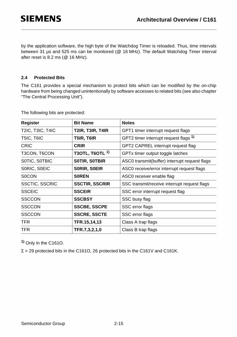
The following bits are protected:
1) Only in the C161O.
Σ = 29 protected bits in the C161O, 26 protected bits in the C161V and C161K.
Register Bit Name Notes
T2IC, T3IC, T4IC T2IR, T3IR, T4IR GPT1 timer interrupt request flags
T5IC, T6IC T5IR, T6IR GPT2 timer interrupt request flags 1)
CRIC CRIR GPT2 CAPREL interrupt request flag
T3CON, T6CON T3OTL, T6OTL 1) GPTx timer output toggle latches
S0TIC, S0TBIC S0TIR, S0TBIR ASC0 transmit(buffer) interrupt request flags
S0RIC, S0EIC S0RIR, S0EIR ASC0 receive/error interrupt request flags
S0CON S0REN ASC0 receiver enable flag
SSCTIC, SSCRIC SSCTIR, SSCRIR SSC transmit/receive interrupt request flags
SSCEIC SSCEIR SSC error interrupt request flag
SSCCON SSCBSY SSC busy flag
SSCCON SSCBE, SSCPE SSC error flags
SSCCON SSCRE, SSCTE SSC error flags
TFR TFR.15,14,13 Class A trap flags
TFR TFR.7,3,2,1,0 Class B trap flags
Semiconductor Group 2-15
15Jul97@11:09h Memory Organization / C161
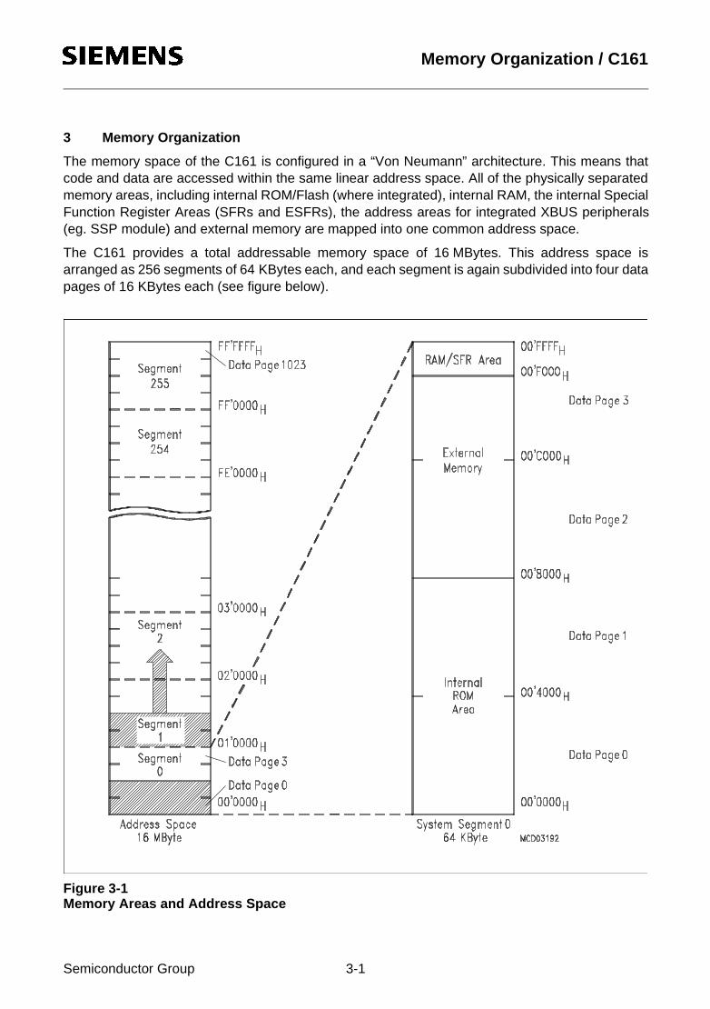
3 Memory Organization
The memory space of the C161 is configured in a “Von Neumann” architecture. This means thatcode and data are accessed within the same linear address space. All of the physically separatedmemory areas, including internal ROM/Flash (where integrated), internal RAM, the internal SpecialFunction Register Areas (SFRs and ESFRs), the address areas for integrated XBUS peripherals(eg. SSP module) and external memory are mapped into one common address space.
The C161 provides a total addressable memory space of 16 MBytes. This address space isarranged as 256 segments of 64 KBytes each, and each segment is again subdivided into four datapages of 16 KBytes each (see figure below).
Figure 3-1Memory Areas and Address Space
Semiconductor Group 3-1
15Jul97@11:09h Memory Organization / C161
Most internal memory areas are mapped into segment 0, the system segment. The upper 4 KByteof segment 0 (00’F000H...00’FFFFH) hold the Internal RAM and Special Function Register Areas(SFR and ESFR). The lower 32 KByte of segment 0 (00’0000H...00’7FFFH) may be occupied by apart of the on-chip ROM or Flash memory and is called the Internal ROM area. This ROM area canbe remapped to segment 1 (01’0000H...01’7FFFH), to enable external memory access in the lowerhalf of segment 0, or the internal ROM may be disabled at all.
Code and data may be stored in any part of the internal memory areas, except for the SFR blocks,which may be used for control / data, but not for instructions.
Note: Accesses to the internal ROM area on ROMless devices will produce unpredictable results.
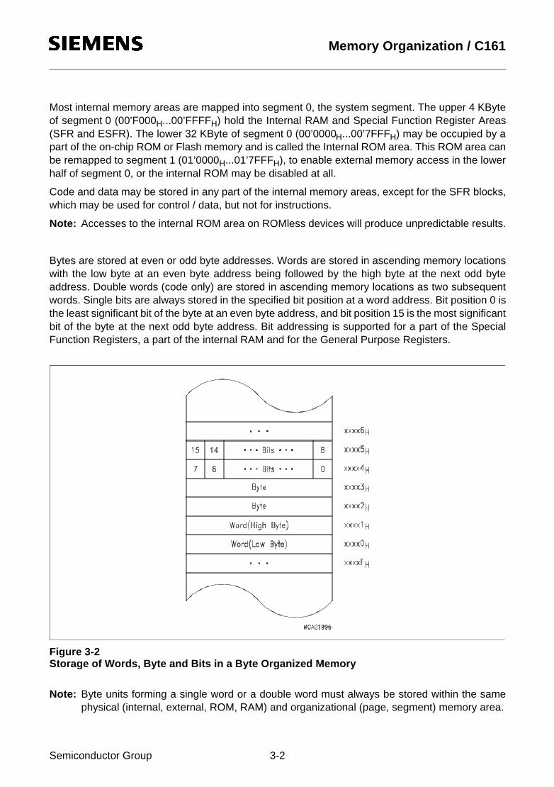
Bytes are stored at even or odd byte addresses. Words are stored in ascending memory locationswith the low byte at an even byte address being followed by the high byte at the next odd byteaddress. Double words (code only) are stored in ascending memory locations as two subsequentwords. Single bits are always stored in the specified bit position at a word address. Bit position 0 isthe least significant bit of the byte at an even byte address, and bit position 15 is the most significantbit of the byte at the next odd byte address. Bit addressing is supported for a part of the SpecialFunction Registers, a part of the internal RAM and for the General Purpose Registers.
Figure 3-2Storage of Words, Byte and Bits in a Byte Organized Memory
Note: Byte units forming a single word or a double word must always be stored within the samephysical (internal, external, ROM, RAM) and organizational (page, segment) memory area.
Semiconductor Group 3-2
15Jul97@11:09h Memory Organization / C161
3.1 Internal ROM
The C161 may reserve an address area of variable size (depending on the version) for on-chipmask-programmable ROM (organized as X * 32) or Flash memory. The lower 32 KByte of the on-chip ROM/Flash are referred to as “Internal ROM Area”. Internal ROM accesses are globallyenabled or disabled via bit ROMEN in register SYSCON. This bit is set during reset according to thelevel on pin EA, or may be altered via software. If enabled, the internal ROM area occupies thelower 32 KByte of either segment 0 or segment 1. This ROM mapping is controlled by bit ROMS1in register SYSCON.
Note: The size of the internal ROM area is independent of the size of the actual implemented ROM.Also devices with less than 32 KByte of ROM or with no ROM at all will have this 32 KBytearea occupied, if the ROM is enabled. Devices with larger ROMs provide the mapping optiononly for the ROM area.
Devices with a ROM size above 32 KByte expand the ROM area from the middle of segment 1, ie.starting at address 01’8000H.
The internal ROM/Flash can be used for both code (instructions) and data (constants, tables, etc.)storage.
Code fetches are always made on even byte addresses. The highest possible code storage locationin the internal ROM is either xx’xxFEH for single word instructions, or xx’xxFCH for double wordinstructions. The respective location must contain a branch instruction (unconditional), becausesequential boundary crossing from internal ROM to external memory is not supported and causeserroneous results.
Any word and byte data read accesses may use the indirect or long 16-bit addressing modes. Thereis no short addressing mode for internal ROM operands. Any word data access is made to an evenbyte address. The highest possible word data storage location in the internal ROM is xx’xxFEH. ForPEC data transfers the internal ROM can be accessed independent of the contents of the DPPregisters via the PEC source and destination pointers.
The internal ROM is not provided for single bit storage, and therefore it is not bit addressable.
Note: The ‘x’ in the locations above depend on the available ROM/Flash memory and on themapping.
The internal ROM may be enabled, disabled or mapped into segment 0 or segment 1 undersoftware control. Chapter “System Programming” shows how to do this and reminds of theprecautions that must be taken in order to prevent the system from crashing.
Semiconductor Group 3-3

15Jul97@10:59h Memory Organization / C161
3.2 Internal RAM and SFR Area
The RAM/SFR area is located within data page 3 and provides access to the on-chip RAM (IRAM,organized as xK*16) and to two 512 Byte blocks of Special Function Registers (SFRs).
The C161O provides 2 KByte of IRAM, the C161V and the C161K provide 1 KByte.The internal RAM serves for several purposes:• System Stack (programmable size)• General Purpose Register Banks (GPRs)• Source and destination pointers for the Peripheral Event Controller (PEC)• Variable and other data storage, or• Code storage.
Figure 3-3Internal RAM Area and SFR Areas
Note: The upper 256 Bytes of SFR area, ESFR area and internal RAM are bit-addressable (seeshaded blocks in the figure above).
Semiconductor Group 3-4
15Jul97@11:09h Memory Organization / C161
Code accesses are always made on even byte addresses. The highest possible code storagelocation in the internal RAM is either 00’FDFEH for single word instructions or 00’FDFCH for doubleword instructions. The respective location must contain a branch instruction (unconditional),because sequential boundary crossing from internal RAM to the SFR area is not supported andcauses erroneous results.
Any word and byte data in the internal RAM can be accessed via indirect or long 16-bit addressingmodes, if the selected DPP register points to data page 3. Any word data access is made on aneven byte address. The highest possible word data storage location in the internal RAM is00’FDFEH. For PEC data transfers, the internal RAM can be accessed independent of the contentsof the DPP registers via the PEC source and destination pointers.
The upper 256 Byte of the internal RAM (00’FD00H through 00’FDFFH) and the GPRs of the currentbank are provided for single bit storage, and thus they are bit addressable.
System Stack
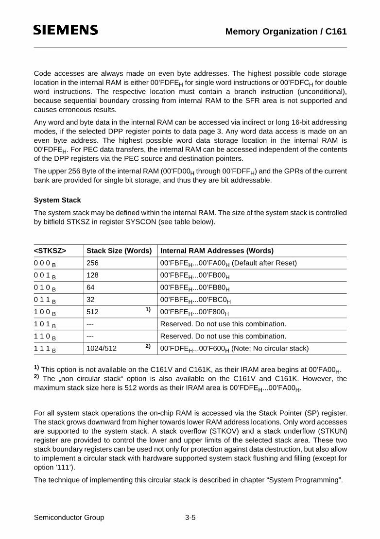
The system stack may be defined within the internal RAM. The size of the system stack is controlledby bitfield STKSZ in register SYSCON (see table below).
1) This option is not available on the C161V and C161K, as their IRAM area begins at 00’FA00H.2) The „non circular stack“ option is also available on the C161V and C161K. However, themaximum stack size here is 512 words as their IRAM area is 00’FDFEH...00’FA00H.
For all system stack operations the on-chip RAM is accessed via the Stack Pointer (SP) register.The stack grows downward from higher towards lower RAM address locations. Only word accessesare supported to the system stack. A stack overflow (STKOV) and a stack underflow (STKUN)register are provided to control the lower and upper limits of the selected stack area. These twostack boundary registers can be used not only for protection against data destruction, but also allowto implement a circular stack with hardware supported system stack flushing and filling (except foroption ’111’).
The technique of implementing this circular stack is described in chapter “System Programming”.
<STKSZ> Stack Size (Words) Internal RAM Addresses (Words)
0 0 0 B 256 00’FBFEH...00’FA00H (Default after Reset)
0 0 1 B 128 00’FBFEH...00’FB00H
0 1 0 B 64 00’FBFEH...00’FB80H
0 1 1 B 32 00’FBFEH...00’FBC0H
1 0 0 B 512 1) 00’FBFEH...00’F800H
1 0 1 B --- Reserved. Do not use this combination.
1 1 0 B --- Reserved. Do not use this combination.
1 1 1 B 1024/512 2) 00’FDFEH...00’F600H (Note: No circular stack)
Semiconductor Group 3-5
15Jul97@11:09h Memory Organization / C161
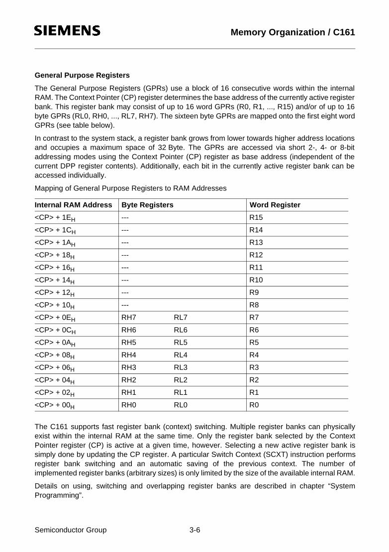
General Purpose Registers
The General Purpose Registers (GPRs) use a block of 16 consecutive words within the internalRAM. The Context Pointer (CP) register determines the base address of the currently active registerbank. This register bank may consist of up to 16 word GPRs (R0, R1, ..., R15) and/or of up to 16byte GPRs (RL0, RH0, ..., RL7, RH7). The sixteen byte GPRs are mapped onto the first eight wordGPRs (see table below).
In contrast to the system stack, a register bank grows from lower towards higher address locationsand occupies a maximum space of 32 Byte. The GPRs are accessed via short 2-, 4- or 8-bitaddressing modes using the Context Pointer (CP) register as base address (independent of thecurrent DPP register contents). Additionally, each bit in the currently active register bank can beaccessed individually.
Mapping of General Purpose Registers to RAM Addresses
The C161 supports fast register bank (context) switching. Multiple register banks can physicallyexist within the internal RAM at the same time. Only the register bank selected by the ContextPointer register (CP) is active at a given time, however. Selecting a new active register bank issimply done by updating the CP register. A particular Switch Context (SCXT) instruction performsregister bank switching and an automatic saving of the previous context. The number ofimplemented register banks (arbitrary sizes) is only limited by the size of the available internal RAM.
Details on using, switching and overlapping register banks are described in chapter “SystemProgramming”.
Internal RAM Address Byte Registers Word Register
<CP> + 1EH --- R15
<CP> + 1CH --- R14
<CP> + 1AH --- R13
<CP> + 18H --- R12
<CP> + 16H --- R11
<CP> + 14H --- R10
<CP> + 12H --- R9
<CP> + 10H --- R8
<CP> + 0EH RH7 RL7 R7
<CP> + 0CH RH6 RL6 R6
<CP> + 0AH RH5 RL5 R5
<CP> + 08H RH4 RL4 R4
<CP> + 06H RH3 RL3 R3
<CP> + 04H RH2 RL2 R2
<CP> + 02H RH1 RL1 R1
<CP> + 00H RH0 RL0 R0
Semiconductor Group 3-6

15Jul97@11:09h Memory Organization / C161
PEC Source and Destination Pointers
The 16 word locations in the internal RAM from 00’FCE0H to 00’FCFEH (just below the bit-addressable section) are provided as source and destination address pointers for data transfers onthe eight PEC channels. Each channel uses a pair of pointers stored in two subsequent wordlocations with the source pointer (SRCPx) on the lower and the destination pointer (DSTPx) on thehigher word address (x = 7...0).
Figure 3-4Location of the PEC Pointers
Whenever a PEC data transfer is performed, the pair of source and destination pointers, which isselected by the specified PEC channel number, is accessed independent of the current DPPregister contents and also the locations referred to by these pointers are accessed independent ofthe current DPP register contents. If a PEC channel is not used, the corresponding pointer locationsarea available and can be used for word or byte data storage.
For more details about the use of the source and destination pointers for PEC data transfers seesection “Interrupt and Trap Functions”.
Semiconductor Group 3-7

15Jul97@11:09h Memory Organization / C161
Special Function Registers
The functions of the CPU, the bus interface, the IO ports and the on-chip peripherals of the C161 arecontrolled via a number of so-called Special Function Registers (SFRs). These SFRs are arrangedwithin two areas of 512 Byte size each. The first register block, the SFR area, is located in the 512Bytes above the internal RAM (00’FFFFH...00’FE00H), the second register block, the Extended SFR(ESFR) area, is located in the 512 Bytes below the internal RAM (00’F1FFH...00’F000H).
Special function registers can be addressed via indirect and long 16-bit addressing modes. Usingan 8-bit offset together with an implicit base address allows to address word SFRs and theirrespective low bytes. However, this does not work for the respective high bytes!
Note: Writing to any byte of an SFR causes the non-addressed complementary byte to be cleared!
The upper half of each register block is bit-addressable, so the respective control/status bits candirectly be modified or checked using bit addressing.
When accessing registers in the ESFR area using 8-bit addresses or direct bit addressing, anExtend Register (EXTR) instruction is required before, to switch the short addressing mechanismfrom the standard SFR area to the Extended SFR area. This is not required for 16-bit and indirectaddresses. The GPRs R15...R0 are duplicated, ie. they are accessible within both register blocksvia short 2-, 4- or 8-bit addresses without switching.
Example:
EXTR #4 ;Switch to ESFR area for the next 4 instructionsMOV ODP2, #data16 ;ODP2 uses 8-bit reg addressingBFLDL DP6, #mask, #data8 ;Bit addressing for bit fieldsBSET DP1H.7 ;Bit addressing for single bitsMOV T8REL, R1 ;T8REL uses 16-bit address, R1 is duplicated...
;...and also accessible via the ESFR mode;(EXTR is not required for this access)
;------- ;------------------- ;The scope of the EXTR #4 instruction ends here!
MOV T8REL, R1 ;T8REL uses 16-bit address, R1 is duplicated...;...and does not require switching
In order to minimize the use of the EXTR instructions the ESFR area mostly holds registers whichare mainly required for initialization and mode selection. Registers that need to be accessedfrequently are allocated to the standard SFR area, wherever possible.
Note: The tools are equipped to monitor accesses to the ESFR area and will automatically insertEXTR instructions, or issue a warning in case of missing or excessive EXTR instructions.
Semiconductor Group 3-8

15Jul97@11:09h Memory Organization / C161
3.3 External Memory Space
The C161 is capable of using an address space of up to 4 MByte. Only parts of this address spaceare occupied by internal memory areas. All addresses which are not used for on-chip memory(ROM or RAM) or for registers may reference external memory locations. This external memory isaccessed via the C161’s external bus interface.
Four memory bank sizes are supported:
• Non-segmented mode: 64 KByte with A15...A0 on PORT0 or PORT1• 2-bit segmented mode: 256 KByte with A17...A16 on Port 4 and A15...A0 on PORT0 or PORT1• 4-bit segmented mode: 1 MByte with A19...A16 on Port 4 and A15...A0 on PORT0 or PORT1• 6-bit segmented mode: 4 MByte with A21...A16 on Port 4 and A15...A0 on PORT0 or PORT1
Each bank can be directly addressed via the address bus, while the programmable chip selectsignals can be used to select various memory banks.
The C161 also supports four different bus types:
• Multiplexed 16-bit Bus with address and data on PORT0 (Default after Reset)• Multiplexed 8-bit Bus with address and data on PORT0/P0L• Demultiplexed 16-bit Bus with address on PORT1 and data on PORT0 (not on the C161V)• Demultiplexed 8-bit Bus with address on PORT1 and data on P0L (not on the C161V)
Memory model and bus mode are selected during reset by pin EA and PORT0 pins. For furtherdetails about the external bus configuration and control please refer to chapter "The External BusInterface".
External word and byte data can only be accessed via indirect or long 16-bit addressing modesusing one of the four DPP registers. There is no short addressing mode for external operands. Anyword data access is made to an even byte address.
For PEC data transfers the external memory in segment 0 can be accessed independent of thecontents of the DPP registers via the PEC source and destination pointers.
The external memory is not provided for single bit storage and therefore it is not bit addressable.
Semiconductor Group 3-9
15Jul97@11:09h Memory Organization / C161
3.4 Crossing Memory Boundaries
The address space of the C161 is implicitly divided into equally sized blocks of different granularityand into logical memory areas. Crossing the boundaries between these blocks (code or data) orareas requires special attention to ensure that the controller executes the desired operations.
Memory Areas are partitions of the address space that represent different kinds of memory (ifprovided at all). These memory areas are the internal RAM/SFR area, the internal ROM (ifavailable), the on-chip X-Peripherals (if integrated) and the external memory.
Accessing subsequent data locations that belong to different memory areas is no problem.However, when executing code, the different memory areas must be switched explicitly via branchinstructions. Sequential boundary crossing is not supported and leads to erroneous results.
Note: Changing from the external memory area to the internal RAM/SFR area takes place withinsegment 0.
Segments are contiguous blocks of 64 KByte each. They are referenced via the code segmentpointer CSP for code fetches and via an explicit segment number for data accesses overriding thestandard DPP scheme.During code fetching segments are not changed automatically, but rather must be switchedexplicitly. The instructions JMPS, CALLS and RETS will do this.In larger sequential programs make sure that the highest used code location of a segment containsan unconditional branch instruction to the respective following segment, to prevent the prefetcherfrom trying to leave the current segment.
Data Pages are contiguous blocks of 16 KByte each. They are referenced via the data pagepointers DPP3...0 and via an explicit data page number for data accesses overriding the standardDPP scheme. Each DPP register can select one of the possible 1024 data pages. The DPP registerthat is used for the current access is selected via the two upper bits of the 16-bit data address.Subsequent 16-bit data addresses that cross the 16 KByte data page boundaries therefore will usedifferent data page pointers, while the physical locations need not be subsequent within memory.
Semiconductor Group 3-10

10Jul97@15:19h The Central Processing Unit (CPU) / C161
4 The Central Processing Unit (CPU)
Basic tasks of the CPU are to fetch and decode instructions, to supply operands for the arithmeticand logic unit (ALU), to perform operations on these operands in the ALU, and to store thepreviously calculated results. As the CPU is the main engine of the C161 controller, it is alsoaffected by certain actions of the peripheral subsystem.
Since a four stage pipeline is implemented in the C161, up to four instructions can be processed inparallel. Most instructions of the C161 are executed in one machine cycle (ie. 100 ns @ 20 MHzCPU clock) due to this parallelism. This chapter describes how the pipeline works for sequential andbranch instructions in general, and which hardware provisions have been made to speed theexecution of jump instructions in particular. The general instruction timing is described includingstandard and exceptional timing.
While internal memory accesses are normally performed by the CPU itself, external peripheral ormemory accesses are performed by a particular on-chip External Bus Controller (EBC), which isautomatically invoked by the CPU whenever a code or data address refers to the external addressspace. If possible, the CPU continues operating while an external memory access is in progress. Ifexternal data are required but are not yet available, or if a new external memory access is requestedby the CPU, before a previous access has been completed, the CPU will be held by the EBC untilthe request can be satisfied. The EBC is described in a dedicated chapter.
Figure 4-1CPU Block Diagram
Semiconductor Group 4-1

10Jul97@15:19h The Central Processing Unit (CPU) / C161
The on-chip peripheral units of the C161 work nearly independent of the CPU with a separate clockgenerator. Data and control information is interchanged between the CPU and these peripherals viaSpecial Function Registers (SFRs). Whenever peripherals need a non-deterministic CPU action, anon-chip Interrupt Controller compares all pending peripheral service requests against each otherand prioritizes one of them. If the priority of the current CPU operation is lower than the priority ofthe selected peripheral request, an interrupt will occur.
Basically, there are two types of interrupt processing:
• Standard interrupt processing forces the CPU to save the current program status and the returnaddress on the stack before branching to the interrupt vector jump table.
• PEC interrupt processing steals just one machine cycle from the current CPU activity to performa single data transfer via the on-chip Peripheral Event Controller (PEC).
System errors detected during program execution (socalled hardware traps) or an external non-maskable interrupt are also processed as standard interrupts with a very high priority.
In contrast to other on-chip peripherals, there is a closer conjunction between the watchdog timerand the CPU. If enabled, the watchdog timer expects to be serviced by the CPU within aprogrammable period of time, otherwise it will reset the chip. Thus, the watchdog timer is able toprevent the CPU from going totally astray when executing erroneous code. After reset, thewatchdog timer starts counting automatically, but it can be disabled via software, if desired.
Beside its normal operation there are the following particular CPU states:
• Reset state: Any reset (hardware, software, watchdog) forces the CPU into a predefined activestate.
• IDLE state: The clock signal to the CPU itself is switched off, while the clocks for the on-chipperipherals keep running.
• POWER DOWN state: All of the on-chip clocks are switched off.
A transition into an active CPU state is forced by an interrupt (if being IDLE) or by a reset (if beingin POWER DOWN mode).The IDLE, POWER DOWN and RESET states can be entered by particular C161 system controlinstructions.
A set of Special Function Registers is dedicated to the functions of the CPU core:
• General System Configuration : SYSCON (RP0H)• CPU Status Indication and Control : PSW• Code Access Control : IP, CSP• Data Paging Control : DPP0, DPP1, DPP2, DPP3• GPRs Access Control : CP• System Stack Access Control : SP, STKUN, STKOV• Multiply and Divide Support : MDL, MDH, MDC• ALU Constants Support : ZEROS, ONES
Semiconductor Group 4-2
10Jul97@15:19h The Central Processing Unit (CPU) / C161
4.1 Instruction Pipelining
The instruction pipeline of the C161 partitiones instruction processing into four stages of which eachone has its individual task:
1st –>FETCH:In this stage the instruction selected by the Instruction Pointer (IP) and the Code Segment Pointer(CSP) is fetched from either the internal ROM, internal RAM, or external memory.
2nd –>DECODE:In this stage the instructions are decoded and, if required, the operand addresses are calculatedand the respective operands are fetched. For all instructions, which implicitly access the systemstack, the SP register is either decremented or incremented, as specified. For branch instructionsthe Instruction Pointer and the Code Segment Pointer are updated with the desired branch targetaddress (provided that the branch is taken).
3rd –>EXECUTE:In this stage an operation is performed on the previously fetched operands in the ALU. Additionally,the condition flags in the PSW register are updated as specified by the instruction. All explicit writesto the SFR memory space and all auto-increment or auto-decrement writes to GPRs used asindirect address pointers are performed during the execute stage of an instruction, too.
4th –>WRITE BACK:In this stage all external operands and the remaining operands within the internal RAM space arewritten back.
A particularity of the C161 are the so-called injected instructions. These injected instructions aregenerated internally by the machine to provide the time needed to process instructions, whichcannot be processed within one machine cycle. They are automatically injected into the decodestage of the pipeline, and then they pass through the remaining stages like every standardinstruction. Program interrupts are performed by means of injected instructions, too. Although theseinternally injected instructions will not be noticed in reality, they are introduced here to ease theexplanation of the pipeline in the following.
Sequential Instruction Processing
Each single instruction has to pass through each of the four pipeline stages regardless of whetherall possible stage operations are really performed or not. Since passing through one pipeline stagetakes at least one machine cycle, any isolated instruction takes at least four machine cycles to becompleted. Pipelining, however, allows parallel (ie. simultaneous) processing of up to fourinstructions. Thus, most of the instructions seem to be processed during one machine cycle as soonas the pipeline has been filled once after reset (see figure below).
Instruction pipelining increases the average instruction throughput considered over a certain periodof time. In the following, any execution time specification of an instruction always refers to theaverage execution time due to pipelined parallel instruction processing.
Semiconductor Group 4-3
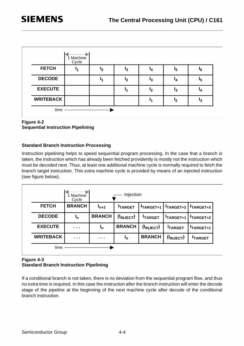
10Jul97@15:19h The Central Processing Unit (CPU) / C161
Figure 4-2Sequential Instruction Pipelining
Standard Branch Instruction Processing
Instruction pipelining helps to speed sequential program processing. In the case that a branch istaken, the instruction which has already been fetched providently is mostly not the instruction whichmust be decoded next. Thus, at least one additional machine cycle is normally required to fetch thebranch target instruction. This extra machine cycle is provided by means of an injected instruction(see figure below).
Figure 4-3Standard Branch Instruction Pipelining
If a conditional branch is not taken, there is no deviation from the sequential program flow, and thusno extra time is required. In this case the instruction after the branch instruction will enter the decodestage of the pipeline at the beginning of the next machine cycle after decode of the conditionalbranch instruction.
1 Machine Cycle
FETCH I2
I1
I3
I2
I1
I4
I3
I2
I1
I6
I5
I4
I3
I5
I4
I3
I2
I1
DECODE
EXECUTE
WRITEBACK
time
1 Machine Cycle
FETCH In+2
BRANCH
In
. . .
ITARGET
(IINJECT)
BRANCH
In
ITARGET+1
ITARGET
(IINJECT)
BRANCH
ITARGET+3
ITARGET+2
ITARGET+1
ITARGET
ITARGET+2
ITARGET+1
ITARGET
(IINJECT)
BRANCH
In
. . .
. . .
DECODE
EXECUTE
WRITEBACK
time
Injection
Semiconductor Group 4-4
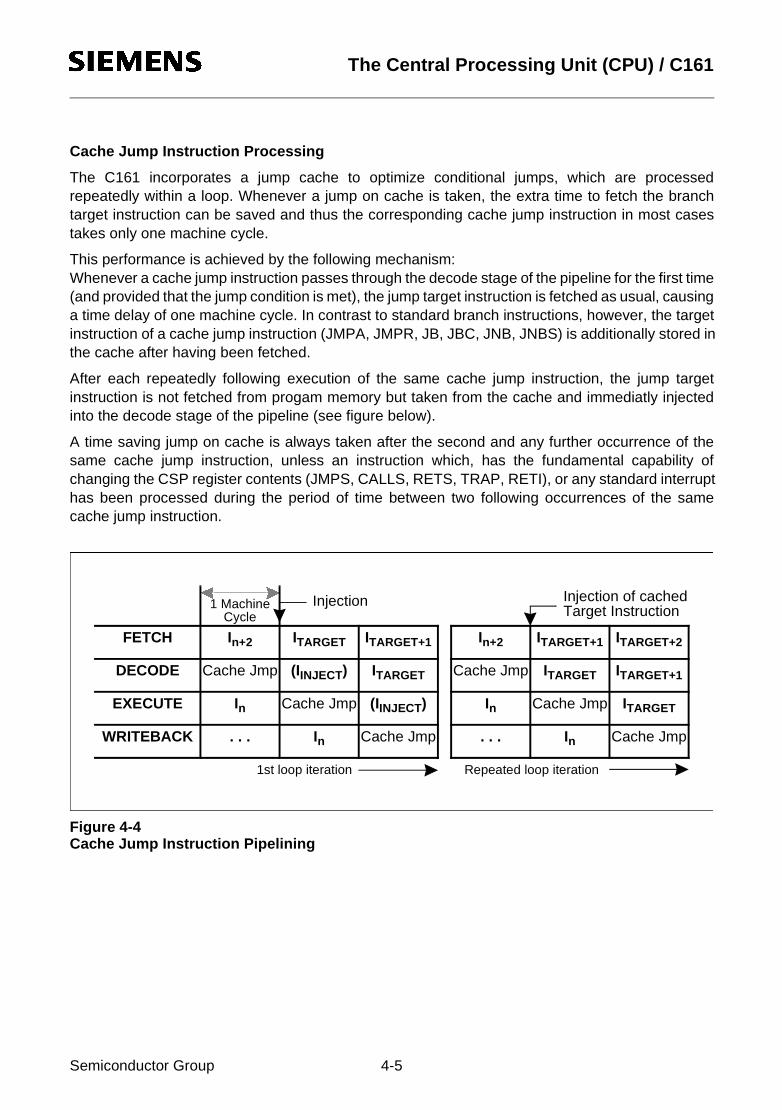
10Jul97@15:19h The Central Processing Unit (CPU) / C161
Cache Jump Instruction Processing
The C161 incorporates a jump cache to optimize conditional jumps, which are processedrepeatedly within a loop. Whenever a jump on cache is taken, the extra time to fetch the branchtarget instruction can be saved and thus the corresponding cache jump instruction in most casestakes only one machine cycle.
This performance is achieved by the following mechanism:Whenever a cache jump instruction passes through the decode stage of the pipeline for the first time(and provided that the jump condition is met), the jump target instruction is fetched as usual, causinga time delay of one machine cycle. In contrast to standard branch instructions, however, the targetinstruction of a cache jump instruction (JMPA, JMPR, JB, JBC, JNB, JNBS) is additionally stored inthe cache after having been fetched.
After each repeatedly following execution of the same cache jump instruction, the jump targetinstruction is not fetched from progam memory but taken from the cache and immediatly injectedinto the decode stage of the pipeline (see figure below).
A time saving jump on cache is always taken after the second and any further occurrence of thesame cache jump instruction, unless an instruction which, has the fundamental capability ofchanging the CSP register contents (JMPS, CALLS, RETS, TRAP, RETI), or any standard interrupthas been processed during the period of time between two following occurrences of the samecache jump instruction.
Figure 4-4Cache Jump Instruction Pipelining
In+2
Cache Jmp
In
. . .
ITARGET+1
ITARGET
Cache Jmp
In
ITARGET+2
ITARGET+1
ITARGET
Cache Jmp
In+2
Cache Jmp
In
. . .
ITARGET
(IINJECT)
Cache Jmp
In
ITARGET+1
ITARGET
(IINJECT)
Cache Jmp
1 Machine Cycle
FETCH
DECODE
EXECUTE
WRITEBACK
1st loop iteration
Injection Injection of cachedTarget Instruction
Repeated loop iteration
Semiconductor Group 4-5

10Jul97@15:19h The Central Processing Unit (CPU) / C161
Particular Pipeline Effects
Since up to four different instructions are processed simultaneously, additional hardware has beenspent in the C161 to consider all causal dependencies which may exist on instructions in differentpipeline stages without a loss of performance. This extra hardware (ie. for ’forwarding’ operand readand write values) resolves most of the possible conflicts (eg. multiple usage of buses) in a timeoptimized way and thus avoids that the pipeline becomes noticeable for the user in most cases.However, there are some very rare cases, where the circumstance that the C161 is a pipelinedmachine requires attention by the programmer. In these cases the delays caused by pipelineconflicts can be used for other instructions in order to optimize performance.
• Context Pointer Updating
An instruction, which calculates a physical GPR operand address via the CP register, is mostly notcapable of using a new CP value, which is to be updated by an immediately preceding instruction.Thus, to make sure that the new CP value is used, at least one instruction must be inserted betweena CP-changing and a subsequent GPR-using instruction, as shown in the following example:
In : SCXT CP, #0FC00h ; select a new contextIn+1 : .... ; must not be an instruction using a GPRIn+2 : MOV R0, #dataX ; write to GPR 0 in the new context
• Data Page Pointer Updating
An instruction, which calculates a physical operand address via a particular DPPn (n=0 to 3)register, is mostly not capable of using a new DPPn register value, which is to be updated by animmediately preceding instruction. Thus, to make sure that the new DPPn register value is used, atleast one instruction must be inserted between a DPPn-changing instruction and a subsequentinstruction which implicitly uses DPPn via a long or indirect addressing mode, as shown in thefollowing example:
In : MOV DPP0, #4 ; select data page 4 via DPP0In+1 : .... ; must not be an instruction using DPP0In+2 : MOV DPP0:0000H, R1 ; move contents of R1 to address location 01’0000H
; (in data page 4) supposed segmentation is enabled
• Explicit Stack Pointer Updating
None of the RET, RETI, RETS, RETP or POP instructions is capable of correctly using a new SPregister value, which is to be updated by an immediately preceding instruction. Thus, in order to usethe new SP register value without erroneously performed stack accesses, at least one instructionmust be inserted between an explicitly SP-writing and any subsequent of the just mentionedimplicitly SP-using instructions, as shown in the following example:
In : MOV SP, #0FA40H ; select a new top of stackIn+1 : .... ; must not be an instruction popping operands
; from the system stackIn+2 : POP R0 ; pop word value from new top of stack into R0
Note: Conflicts with instructions writing to the stack (PUSH, CALL, SCXT) are solved internally bythe CPU logic.
Semiconductor Group 4-6

10Jul97@15:19h The Central Processing Unit (CPU) / C161
• External Memory Access Sequences
The effect described here will only become noticeable, when watching the external memory accesssequences on the external bus (eg. by means of a Logic Analyzer). Different pipeline stages cansimultaneously put a request on the External Bus Controller (EBC). The sequence of instructionsprocessed by the CPU may diverge from the sequence of the corresponding external memoryaccesses performed by the EBC, due to the predefined priority of external memory accesses:
1st Write Data2nd Fetch Code3rd Read Data.
• Controlling Interrupts
Software modifications (implicit or explicit) of the PSW are done in the execute phase of therespective instructions. In order to maintain fast interrupt responses, however, the current interruptprioritization round does not consider these changes, ie. an interrupt request may be acknowledgedafter the instruction that disables interrupts via IEN or ILVL or after the following instructions.Timecritical instruction sequences therefore should not begin directly after the instruction disablinginterrupts, as shown in the following example:
INT_OFF: BCLR IEN ; globally disable interruptsIN-1 ; non-critical instruction
CRIT_1ST: IN ; begin of uninterruptable critical sequence. . .
CRIT_LAST: IN+x ; end of uninterruptable critical sequenceINT_ON: BSET IEN ; globally re-enable interrupts
Note: The described delay of 1 instruction also applies for enabling the interrupts system ie. nointerrupt requests are acknowledged until the instruction following the enabling instruction.
• Initialization of Port Pins
Modifications of the direction of port pins (input or output) become effective only after the instructionfollowing the modifying instruction. As bit instructions (BSET, BCLR) use internal read-modify-writesequences accessing the whole port, instructions modifying the port direction should be followed byan instruction that does not access the same port (see example below).
WRONG: BSET DP3.13 ; change direction of P3.13 to outputBSET P3.5 ; P3.13 is still input, the rd-mod-wr reads pin P3.13
RIGHT: BSET DP3.13 ; change direction of P3.13 to outputNOP ; any instruction not accessing port 3BSET P3.5 ; P3.13 is now output,
; the rd-mod-wr reads the P3.13 output latch
Semiconductor Group 4-7

10Jul97@15:19h The Central Processing Unit (CPU) / C161
• Changing the System Configuration
The instruction following an instruction that changes the system configuration via register SYSCON(eg. the mapping of the internal ROM, segmentation, stack size) cannot use the new resources (eg.ROM or stack). In these cases an instruction that does not access these resources should beinserted. Code accesses to the new ROM area are only possible after an absolute branch to thisarea.
Note: As a rule, instructions that change ROM mapping should be executed from internal RAM orexternal memory.
• BUSCON/ADDRSEL
The instruction following an instruction that changes the properties of an external address areacannot access operands within the new area. In these cases an instruction that does not access thisaddress area should be inserted. Code accesses to the new address area should be made after anabsolute branch to this area.
Note: As a rule, instructions that change external bus properties should not be executed from therespective external memory area.
• Timing
Instruction pipelining reduces the average instruction processing time in a wide scale (from four toone machine cycles, mostly). However, there are some rare cases, where a particular pipelinesituation causes the processing time for a single instruction to be extended either by a half or by onemachine cycle. Although this additional time represents only a tiny part of the total programexecution time, it might be of interest to avoid these pipeline-caused time delays in time criticalprogram modules.
Besides a general execution time description, the following section provides some hints on how tooptimize time-critical program parts with regard to such pipeline-caused timing particularities.
Semiconductor Group 4-8

10Jul97@15:19h The Central Processing Unit (CPU) / C161
4.2 Bit-Handling and Bit-Protection
The C161 provides several mechanisms to manipulate bits. These mechanisms either manipulatesoftware flags within the internal RAM, control on-chip peripherals via control bits in their respectiveSFRs or control IO functions via port pins.
The instructions BSET, BCLR, BAND, BOR, BXOR, BMOV, BMOVN explicitly set or clear specificbits. The instructions BFLDL and BFLDH allow to manipulate up to 8 bits of a specific byte at onetime. The instructions JBC and JNBS implicitly clear or set the specified bit when the jump is taken.The instructions JB and JNB (also conditional jump instructions that refer to flags) evaluate thespecified bit to determine if the jump is to be taken.
Note: Bit operations on undefined bit locations will always read a bit value of ‘0’, while the writeaccess will not effect the respective bit location.
All instructions that manipulate single bits or bit groups internally use a read-modify-write sequencethat accesses the whole word, which contains the specified bit(s).
This method has several consequences:
• Bits can only be modified within the internal address areas, ie. internal RAM and SFRs. Externallocations cannot be used with bit instructions.
The upper 256 bytes of the SFR area, the ESFR area and the internal RAM are bit-addressable (seechapter “Memory Organization”), ie. those register bits located within the respective sections can bedirectly manipulated using bit instructions. The other SFRs must be accessed byte/word wise.
Note: All GPRs are bit-addressable independent of the allocation of the register bank via thecontext pointer CP. Even GPRs which are allocated to not bit-addressable RAM locationsprovide this feature.
• The read-modify-write approach may be critical with hardware-effected bits. In these cases thehardware may change specific bits while the read-modify-write operation is in progress, where thewriteback would overwrite the new bit value generated by the hardware. The solution is either theimplemented hardware protection (see below) or realized through special programming (see“Particular Pipeline Effects”).
Protected bits are not changed during the read-modify-write sequence, ie. when hardware sets eg.an interrupt request flag between the read and the write of the read-modify-write sequence. Thehardware protection logic guarantees that only the intended bit(s) is/are effected by the write-backoperation.
Note: If a conflict occurs between a bit manipulation generated by hardware and an intendedsoftware access the software access has priority and determines the final value of therespective bit.
A summary of the protected bits implemented in the C161 can be found at the end of chapter“Architectural Overview”.
Semiconductor Group 4-9

10Jul97@15:19h The Central Processing Unit (CPU) / C161
4.3 Instruction State Times
Basically, the time to execute an instruction depends on where the instruction is fetched from, andwhere possible operands are read from or written to. The fastest processing mode of the C161 is toexecute a program fetched from the internal ROM. In that case most of the instructions can beprocessed within just one machine cycle, which is also the general minimum execution time.
All external memory accesses are performed by the C161’s on-chip External Bus Controller (EBC),which works in parallel with the CPU.
This section summarizes the execution times in a very condensed way. A detailled description ofthe execution times for the various instructions and the specific exceptions can be found in the“C16x Family Instruction Set Manual” .
The table below shows the minimum execution times required to process a C161 instruction fetchedfrom the internal ROM, the internal RAM or from external memory. These execution times apply tomost of the C161 instructions - except some of the branches, the multiplication, the division and aspecial move instruction. In case of internal ROM program execution there is no execution timedependency on the instruction length except for some special branch situations. The numbers in thetable are in units of [ns], refer to a CPU clock of 20 MHz and assume no waitstates.
Minimum Execution Times
Execution from the internal RAM provides flexibility in terms of loadable and modifyable code on theaccount of execution time.Execution from external memory strongly depends on the selected bus mode and the programmingof the bus cycles (waitstates).
The operand and instruction accesses listed below can extend the execution time of an instruction:
• Internal ROM operand reads (same for byte and word operand reads)• Internal RAM operand reads via indirect addressing modes• Internal SFR operand reads immediately after writing• External operand reads• External operand writes• Jumps to non-aligned double word instructions in the internal ROM space• Testing Branch Conditions immediately after PSW writes
Instruction Fetch Word Operand Access
Memory Area Word Instruction
Doubleword Instruction
Read from Write to
Internal ROM 100 100 100 ---
Internal RAM 300 400 0/50 0
16-bit Demux Bus 100 200 100 100
16-bit Mux Bus 150 300 150 150
8-bit Demux Bus 200 400 200 200
8-bit Mux Bus 300 600 300 300
Semiconductor Group 4-10
10Jul97@15:19h The Central Processing Unit (CPU) / C161
4.4 CPU Special Function Registers
The core CPU requires a set of Special Function Registers (SFRs) to maintain the system stateinformation, to supply the ALU with register-addressable constants and to control system and busconfiguration, multiply and divide ALU operations, code memory segmentation, data memorypaging, and accesses to the General Purpose Registers and the System Stack.
The access mechanism for these SFRs in the CPU core is identical to the access mechanism forany other SFR. Since all SFRs can simply be controlled by means of any instruction, which iscapable of addressing the SFR memory space, a lot of flexibility has been gained, without the needto create a set of system-specific instructions.
Note, however, that there are user access restrictions for some of the CPU core SFRs to ensureproper processor operations. The instruction pointer IP and code segment pointer CSP cannot beaccessed directly at all. They can only be changed indirectly via branch instructions.
The PSW, SP, and MDC registers can be modified not only explicitly by the programmer, but alsoimplicitly by the CPU during normal instruction processing. Note that any explicit write request (viasoftware) to an SFR supersedes a simultaneous modification by hardware of the same register.
Note: Any write operation to a single byte of an SFR clears the non-addressed complementary bytewithin the specified SFR.Non-implemented (reserved) SFR bits cannot be modified, and will always supply a readvalue of ’0’.
The System Configuration Register SYSCON
This bit-addressable register provides general system configuration and control functions. Thereset value for register SYSCON depends on the state of the PORT0 pins during reset (seehardware effectable bits).
Semiconductor Group 4-11

10Jul97@15:19h The Central Processing Unit (CPU) / C161
SYSCON (FF12H / 89H) SFR Reset Value: 0XX0H
Note: Register SYSCON cannot be changed after execution of the EINIT instruction.The function of bits XPER-SHARE, VISIBLE, WRCFG, BYTDIS, ROMEN and ROMS1 isdescribed in more detail in chapter “The External Bus Controller”.
Bit Function
XPER-SHARE XBUS Peripheral Share Mode Control‘0’: External accesses to XBUS peripherals are disabled‘1’: XBUS peripherals are accessible via the external bus during hold mode
VISIBLE Visible Mode Control‘0’: Accesses to XBUS peripherals are done internally‘1’: XBUS peripheral accesses are made visible on the external pins
XPEN XBUS Peripheral Enable Bit‘0’: Accesses to the on-chip X-Peripherals and their functions are disabled‘1’: The on-chip X-Peripherals are enabled and can be accessedNote: This bit is valid only for derivatives that contain X-Peripherals.
WRCFG Write Configuration Control (Set according to pin P0H.0 during reset)‘0’: Pins WR and BHE retain their normal function‘1’: Pin WR acts as WRL, pin BHE acts as WRH
BYTDIS Disable/Enable Control for Pin BHE (Set according to data bus width)‘0’: Pin BHE enabled‘1’: Pin BHE disabled, pin may be used for general purpose IO
ROMEN Internal ROM Enable (Set according to pin EA during reset)‘0’: Internal ROM disabled: accesses to the ROM area use the external bus‘1’: Internal ROM enabled
SGTDIS Segmentation Disable/Enable Control‘0’: Segmentation enabled (CSP is saved/restored during interrupt entry/exit)‘1’: Segmentation disabled (Only IP is saved/restored)
ROMS1 Internal ROM Mapping‘0’: Internal ROM area mapped to segment 0 (00’0000H...00’7FFFH)‘1’: Internal ROM area mapped to segment 1 (01’0000H...01’7FFFH)
STKSZ System Stack SizeSelects the size of the system stack (in the internal RAM) from 32 to 1024 words
-- XPENXPER-SHARE
VISIBLE- - -
ROMS1
WRCFG
5 4 3 2 1 011 10 9 8 7 615 14 13 12
- - rwrw rw rwrw rw
STKSZSGTDIS
ROMEN
rw
BYTDIS
- - rw rw-
Semiconductor Group 4-12
10Jul97@15:19h The Central Processing Unit (CPU) / C161
Segmentation Disable/Enable Control (SGTDIS) Bit SGTDIS allows to select either the segmented or non-segmented memory mode.In non-segmented memory mode (SGTDIS=’1’) it is assumed that the code address space isrestricted to 64 KBytes (segment 0) and thus 16 bits are sufficient to represent all code addresses.For implicit stack operations (CALL or RET) the CSP register is totally ignored and only the IP issaved to and restored from the stack.In segmented memory mode (SGTDIS=’0’) it is assumed that the whole address space isavailable for instructions. For implicit stack operations (CALL or RET) the CSP register and the IPare saved to and restored from the stack. After reset the segmented memory mode is selected.
Note: Bit SGTDIS controls if the CSP register is pushed onto the system stack in addition to the IPregister before an interrupt service routine is entered, and it is repopped when the interruptservice routine is left again.
System Stack Size (STKSZ)
This bitfield defines the size of the physical system stack, which is located in the internal RAM of theC161. An area of 32...512 words (256 words in the C161V and C161K) or all of the internal RAMmay be dedicated to the system stack. A so-called “circular stack” mechanism allows to use a biggervirtual stack than this dedicated RAM area.
These techniques as well as the encoding of bitfield STKSZ are described in more detail in chapter“System Programming”.
Semiconductor Group 4-13
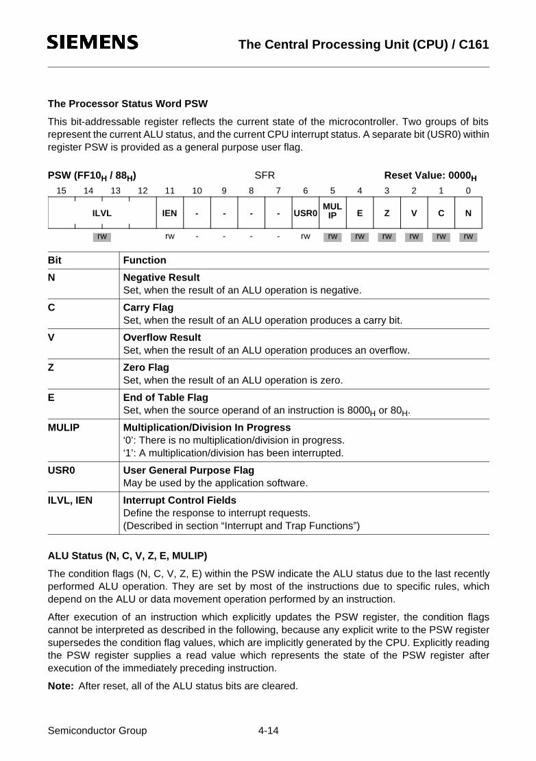
10Jul97@15:19h The Central Processing Unit (CPU) / C161
The Processor Status Word PSW
This bit-addressable register reflects the current state of the microcontroller. Two groups of bitsrepresent the current ALU status, and the current CPU interrupt status. A separate bit (USR0) withinregister PSW is provided as a general purpose user flag.
PSW (FF10H / 88H) SFR Reset Value: 0000H
ALU Status (N, C, V, Z, E, MULIP)
The condition flags (N, C, V, Z, E) within the PSW indicate the ALU status due to the last recentlyperformed ALU operation. They are set by most of the instructions due to specific rules, whichdepend on the ALU or data movement operation performed by an instruction.
After execution of an instruction which explicitly updates the PSW register, the condition flagscannot be interpreted as described in the following, because any explicit write to the PSW registersupersedes the condition flag values, which are implicitly generated by the CPU. Explicitly readingthe PSW register supplies a read value which represents the state of the PSW register afterexecution of the immediately preceding instruction.
Note: After reset, all of the ALU status bits are cleared.
Bit Function
N Negative ResultSet, when the result of an ALU operation is negative.
C Carry FlagSet, when the result of an ALU operation produces a carry bit.
V Overflow ResultSet, when the result of an ALU operation produces an overflow.
Z Zero FlagSet, when the result of an ALU operation is zero.
E End of Table FlagSet, when the source operand of an instruction is 8000H or 80H.
MULIP Multiplication/Division In Progress‘0’: There is no multiplication/division in progress.‘1’: A multiplication/division has been interrupted.
USR0 User General Purpose FlagMay be used by the application software.
ILVL, IEN Interrupt Control FieldsDefine the response to interrupt requests.(Described in section “Interrupt and Trap Functions”)
--MUL
IPUSR0 NZ CVE
5 4 3 2 1 011 10 9 8 7 615 14 13 12
rw rw rw rw- rw rw rw-rw --
IEN --ILVL
rw
Semiconductor Group 4-14

10Jul97@15:19h The Central Processing Unit (CPU) / C161
• N-Flag: For most of the ALU operations, the N-flag is set to ’1’, if the most significant bit of theresult contains a ’1’, otherwise it is cleared. In the case of integer operations the N-flag can beinterpreted as the sign bit of the result (negative: N=’1’, positive: N=’0’). Negative numbers arealways represented as the 2's complement of the corresponding positive number. The range ofsigned numbers extends from '–8000H' to '+7FFFH' for the word data type, or from '–80H' to '+7FH'for the byte data type.For Boolean bit operations with only one operand the N-flag represents theprevious state of the specified bit. For Boolean bit operations with two operands the N-flagrepresents the logical XORing of the two specified bits.
• C-Flag: After an addition the C-flag indicates that a carry from the most significant bit of thespecified word or byte data type has been generated. After a subtraction or a comparison the C-flagindicates a borrow, which represents the logical negation of a carry for the addition.This means that the C-flag is set to ’1’, if no carry from the most significant bit of the specified wordor byte data type has been generated during a subtraction, which is performed internally by the ALUas a 2’s complement addition, and the C-flag is cleared when this complement addition caused acarry.The C-flag is always cleared for logical, multiply and divide ALU operations, because theseoperations cannot cause a carry anyhow.For shift and rotate operations the C-flag represents the value of the bit shifted out last. If a shiftcount of zero is specified, the C-flag will be cleared. The C-flag is also cleared for a prioritize ALUoperation, because a ’1’ is never shifted out of the MSB during the normalization of an operand.For Boolean bit operations with only one operand the C-flag is always cleared. For Boolean bitoperations with two operands the C-flag represents the logical ANDing of the two specified bits.
• V-Flag: For addition, subtraction and 2’s complementation the V-flag is always set to ’1’, if theresult overflows the maximum range of signed numbers, which are representable by either 16 bitsfor word operations ('–8000H' to '+7FFFH'), or by 8 bits for byte operations ('–80H' to '+7FH'),otherwise the V-flag is cleared. Note that the result of an integer addition, integer subtraction, or 2'scomplement is not valid, if the V-flag indicates an arithmetic overflow.For multiplication and division the V-flag is set to '1', if the result cannot be represented in a worddata type, otherwise it is cleared. Note that a division by zero will always cause an overflow. Incontrast to the result of a division, the result of a multiplication is valid regardless of whether the V-flag is set to '1' or not.Since logical ALU operations cannot produce an invalid result, the V-flag is cleared by theseoperations.
The V-flag is also used as 'Sticky Bit' for rotate right and shift right operations. With only using theC-flag, a rounding error caused by a shift right operation can be estimated up to a quantity of onehalf of the LSB of the result. In conjunction with the V-flag, the C-flag allows evaluating the roundingerror with a finer resolution (see table below).For Boolean bit operations with only one operand the V-flag is always cleared. For Boolean bitoperations with two operands the V-flag represents the logical ORing of the two specified bits.
Semiconductor Group 4-15
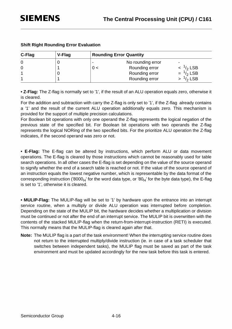
10Jul97@15:19h The Central Processing Unit (CPU) / C161
Shift Right Rounding Error Evaluation
• Z-Flag: The Z-flag is normally set to ’1’, if the result of an ALU operation equals zero, otherwise itis cleared.For the addition and subtraction with carry the Z-flag is only set to ’1’, if the Z-flag already containsa ’1’ and the result of the current ALU operation additionally equals zero. This mechanism isprovided for the support of multiple precision calculations.For Boolean bit operations with only one operand the Z-flag represents the logical negation of theprevious state of the specified bit. For Boolean bit operations with two operands the Z-flagrepresents the logical NORing of the two specified bits. For the prioritize ALU operation the Z-flagindicates, if the second operand was zero or not.
• E-Flag: The E-flag can be altered by instructions, which perform ALU or data movementoperations. The E-flag is cleared by those instructions which cannot be reasonably used for tablesearch operations. In all other cases the E-flag is set depending on the value of the source operandto signify whether the end of a search table is reached or not. If the value of the source operand ofan instruction equals the lowest negative number, which is representable by the data format of thecorresponding instruction (’8000H’ for the word data type, or ’80H’ for the byte data type), the E-flagis set to ’1’, otherwise it is cleared.
• MULIP-Flag: The MULIP-flag will be set to ’1’ by hardware upon the entrance into an interruptservice routine, when a multiply or divide ALU operation was interrupted before completion.Depending on the state of the MULIP bit, the hardware decides whether a multiplication or divisionmust be continued or not after the end of an interrupt service. The MULIP bit is overwritten with thecontents of the stacked MULIP-flag when the return-from-interrupt-instruction (RETI) is executed.This normally means that the MULIP-flag is cleared again after that.
Note: The MULIP flag is a part of the task environment! When the interrupting service routine doesnot return to the interrupted multiply/divide instruction (ie. in case of a task scheduler thatswitches between independent tasks), the MULIP flag must be saved as part of the taskenvironment and must be updated accordingly for the new task before this task is entered.
C-Flag V-Flag Rounding Error Quantity
0011
0101
- No rounding error -0 < Rounding error < 1/2 LSB
Rounding error = 1/2 LSBRounding error > 1/2 LSB
Semiconductor Group 4-16

10Jul97@15:19h The Central Processing Unit (CPU) / C161
CPU Interrupt Status (IEN, ILVL)
The Interrupt Enable bit allows to globally enable (IEN=’1’) or disable (IEN=’0’) interrupts. The four-bit Interrupt Level field (ILVL) specifies the priority of the current CPU activity. The interrupt level isupdated by hardware upon entry into an interrupt service routine, but it can also be modified viasoftware to prevent other interrupts from being acknowledged. In case an interrupt level '15' hasbeen assigned to the CPU, it has the highest possible priority, and thus the current CPU operationcannot be interrupted except by hardware traps or external non-maskable interrupts. For detailsplease refer to chapter “Interrupt and Trap Functions”.
After reset all interrupts are globally disabled, and the lowest priority (ILVL=0) is assigned to theinitial CPU activity.
The Instruction Pointer IP
This register determines the 16-bit intra-segment address of the currently fetched instruction withinthe code segment selected by the CSP register. The IP register is not mapped into the C161'saddress space, and thus it is not directly accessable by the programmer. The IP can, however, bemodified indirectly via the stack by means of a return instruction.
The IP register is implicitly updated by the CPU for branch instructions and after instruction fetchoperations.
IP (---- / --) --- Reset Value: 0000H
Bit Function
ip Specifies the intra segment offset, from where the current instruction is to be fetched. IP refers to the current segment <SEGNR>.
5 4 3 2 1 011 10 9 8 7 615 14 13 12
(r)(w)
ip
Semiconductor Group 4-17
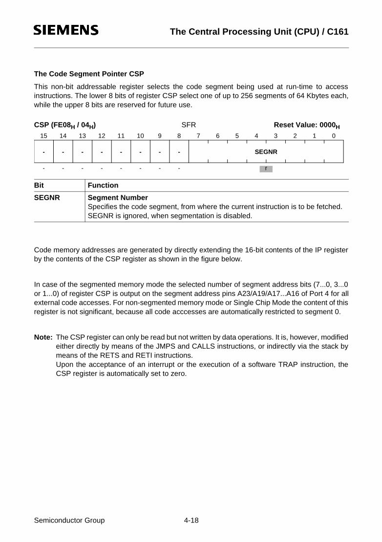
10Jul97@15:19h The Central Processing Unit (CPU) / C161
The Code Segment Pointer CSP
This non-bit addressable register selects the code segment being used at run-time to accessinstructions. The lower 8 bits of register CSP select one of up to 256 segments of 64 Kbytes each,while the upper 8 bits are reserved for future use.
CSP (FE08H / 04H) SFR Reset Value: 0000H
Code memory addresses are generated by directly extending the 16-bit contents of the IP registerby the contents of the CSP register as shown in the figure below.
In case of the segmented memory mode the selected number of segment address bits (7...0, 3...0or 1...0) of register CSP is output on the segment address pins A23/A19/A17...A16 of Port 4 for allexternal code accesses. For non-segmented memory mode or Single Chip Mode the content of thisregister is not significant, because all code acccesses are automatically restricted to segment 0.
Note: The CSP register can only be read but not written by data operations. It is, however, modifiedeither directly by means of the JMPS and CALLS instructions, or indirectly via the stack bymeans of the RETS and RETI instructions.Upon the acceptance of an interrupt or the execution of a software TRAP instruction, theCSP register is automatically set to zero.
Bit Function
SEGNR Segment NumberSpecifies the code segment, from where the current instruction is to be fetched. SEGNR is ignored, when segmentation is disabled.
- -- --
5 4 3 2 1 011 10 9 8 7 615 14 13 12
- - - r-- --
- --
-
SEGNR
Semiconductor Group 4-18

10Jul97@15:19h The Central Processing Unit (CPU) / C161
Figure 4-5Addressing via the Code Segment Pointer
Note: When segmentation is disabled, the IP value is used directly as the 16-bit address.
Semiconductor Group 4-19

10Jul97@15:19h The Central Processing Unit (CPU) / C161
The Data Page Pointers DPP0, DPP1, DPP2, DPP3
These four non-bit addressable registers select up to four different data pages being activesimultaneously at run-time. The lower 10 bits of each DPP register select one of the 1024 possible16-Kbyte data pages while the upper 6 bits are reserved for future use. The DPP registers allow toaccess the entire memory space in pages of 16 Kbytes each.
The DPP registers are implicitly used, whenever data accesses to any memory location are madevia indirect or direct long 16-bit addressing modes (except for override accesses via EXTendedinstructions and PEC data transfers). After reset, the Data Page Pointers are initialized in a way thatall indirect or direct long 16-bit addresses result in identical 18-bit addresses. This allows to accessdata pages 3...0 within segment 0 as shown in the figure below. If the user does not want to use anydata paging, no further action is required.
DPP0 (FE00H / 00H) SFR Reset Value: 0000H
DPP1 (FE02H / 01H) SFR Reset Value: 0001H
DPP2 (FE04H / 02H) SFR Reset Value: 0002H
DPP3 (FE06H / 03H) SFR Reset Value: 0003H
Bit Function
DPPxPN Data Page Number of DPPxSpecifies the data page selected via DPPx. Only the least significant two bits of DPPx are significant, when segmentation is disabled.
- --
5 4 3 2 1 011 10 9 8 7 615 14 13 12
- rw-- --
- --
-
DPP0PN
- --
5 4 3 2 1 011 10 9 8 7 615 14 13 12
- rw-- --
- --
-
DPP1PN
- --
5 4 3 2 1 011 10 9 8 7 615 14 13 12
- rw-- --
- --
-
DPP2PN
- --
5 4 3 2 1 011 10 9 8 7 615 14 13 12
- rw-- --
- --
-
DPP3PN
Semiconductor Group 4-20
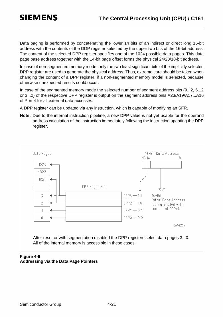
10Jul97@15:19h The Central Processing Unit (CPU) / C161
Data paging is performed by concatenating the lower 14 bits of an indirect or direct long 16-bitaddress with the contents of the DDP register selected by the upper two bits of the 16-bit address.The content of the selected DPP register specifies one of the 1024 possible data pages. This datapage base address together with the 14-bit page offset forms the physical 24/20/18-bit address.
In case of non-segmented memory mode, only the two least significant bits of the implicitly selectedDPP register are used to generate the physical address. Thus, extreme care should be taken whenchanging the content of a DPP register, if a non-segmented memory model is selected, becauseotherwise unexpected results could occur.
In case of the segmented memory mode the selected number of segment address bits (9...2, 5...2or 3...2) of the respective DPP register is output on the segment address pins A23/A19/A17...A16of Port 4 for all external data accesses.
A DPP register can be updated via any instruction, which is capable of modifying an SFR.
Note: Due to the internal instruction pipeline, a new DPP value is not yet usable for the operandaddress calculation of the instruction immediately following the instruction updating the DPPregister.
Figure 4-6Addressing via the Data Page Pointers
After reset or with segmentation disabled the DPP registers select data pages 3...0.All of the internal memory is accessible in these cases.
Semiconductor Group 4-21
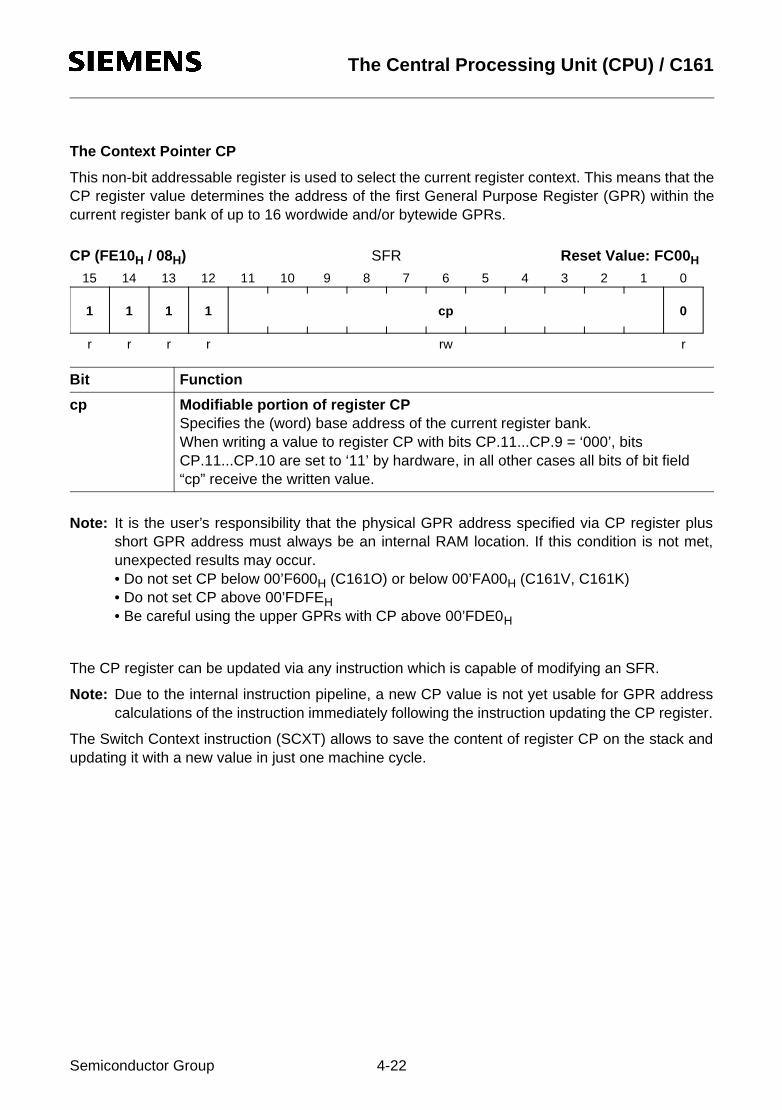
10Jul97@15:19h The Central Processing Unit (CPU) / C161
The Context Pointer CP
This non-bit addressable register is used to select the current register context. This means that theCP register value determines the address of the first General Purpose Register (GPR) within thecurrent register bank of up to 16 wordwide and/or bytewide GPRs.
CP (FE10H / 08H) SFR Reset Value: FC00H
Note: It is the user’s responsibility that the physical GPR address specified via CP register plusshort GPR address must always be an internal RAM location. If this condition is not met,unexpected results may occur.• Do not set CP below 00’F600H (C161O) or below 00’FA00H (C161V, C161K)• Do not set CP above 00’FDFEH• Be careful using the upper GPRs with CP above 00’FDE0H
The CP register can be updated via any instruction which is capable of modifying an SFR.
Note: Due to the internal instruction pipeline, a new CP value is not yet usable for GPR addresscalculations of the instruction immediately following the instruction updating the CP register.
The Switch Context instruction (SCXT) allows to save the content of register CP on the stack andupdating it with a new value in just one machine cycle.
Bit Function
cp Modifiable portion of register CPSpecifies the (word) base address of the current register bank.When writing a value to register CP with bits CP.11...CP.9 = ‘000’, bits CP.11...CP.10 are set to ‘11’ by hardware, in all other cases all bits of bit field “cp” receive the written value.
1 01
5 4 3 2 1 011 10 9 8 7 615 14 13 12
rrwr rr
1 1
r
cp
Semiconductor Group 4-22
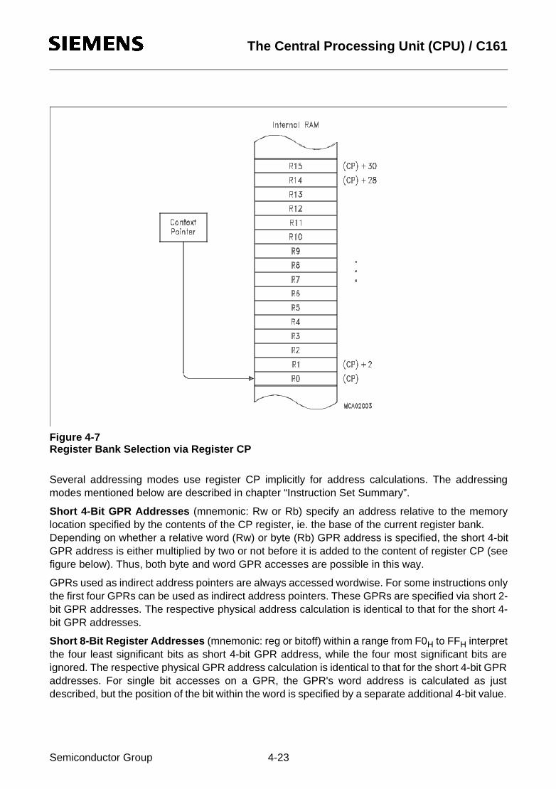
10Jul97@15:19h The Central Processing Unit (CPU) / C161
Figure 4-7Register Bank Selection via Register CP
Several addressing modes use register CP implicitly for address calculations. The addressingmodes mentioned below are described in chapter “Instruction Set Summary”.
Short 4-Bit GPR Addresses (mnemonic: Rw or Rb) specify an address relative to the memorylocation specified by the contents of the CP register, ie. the base of the current register bank.Depending on whether a relative word (Rw) or byte (Rb) GPR address is specified, the short 4-bitGPR address is either multiplied by two or not before it is added to the content of register CP (seefigure below). Thus, both byte and word GPR accesses are possible in this way.
GPRs used as indirect address pointers are always accessed wordwise. For some instructions onlythe first four GPRs can be used as indirect address pointers. These GPRs are specified via short 2-bit GPR addresses. The respective physical address calculation is identical to that for the short 4-bit GPR addresses.
Short 8-Bit Register Addresses (mnemonic: reg or bitoff) within a range from F0H to FFH interpretthe four least significant bits as short 4-bit GPR address, while the four most significant bits areignored. The respective physical GPR address calculation is identical to that for the short 4-bit GPRaddresses. For single bit accesses on a GPR, the GPR's word address is calculated as justdescribed, but the position of the bit within the word is specified by a separate additional 4-bit value.
Semiconductor Group 4-23
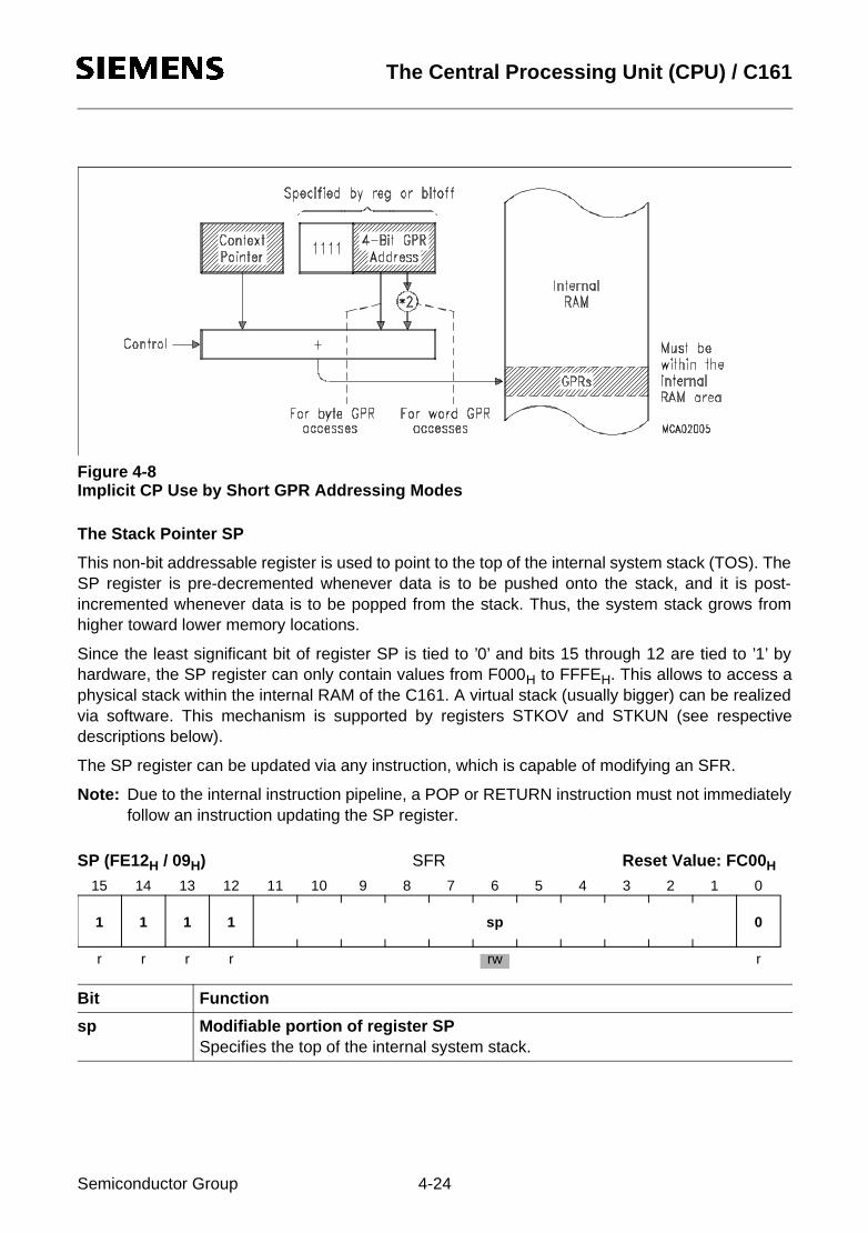
10Jul97@15:19h The Central Processing Unit (CPU) / C161
Figure 4-8Implicit CP Use by Short GPR Addressing Modes
The Stack Pointer SP
This non-bit addressable register is used to point to the top of the internal system stack (TOS). TheSP register is pre-decremented whenever data is to be pushed onto the stack, and it is post-incremented whenever data is to be popped from the stack. Thus, the system stack grows fromhigher toward lower memory locations.
Since the least significant bit of register SP is tied to ’0’ and bits 15 through 12 are tied to ’1’ byhardware, the SP register can only contain values from F000H to FFFEH. This allows to access aphysical stack within the internal RAM of the C161. A virtual stack (usually bigger) can be realizedvia software. This mechanism is supported by registers STKOV and STKUN (see respectivedescriptions below).
The SP register can be updated via any instruction, which is capable of modifying an SFR.
Note: Due to the internal instruction pipeline, a POP or RETURN instruction must not immediatelyfollow an instruction updating the SP register.
SP (FE12H / 09H) SFR Reset Value: FC00H
Bit Function
sp Modifiable portion of register SPSpecifies the top of the internal system stack.
1 01
5 4 3 2 1 011 10 9 8 7 615 14 13 12
rrwr rr
1 1
r
sp
Semiconductor Group 4-24

10Jul97@15:19h The Central Processing Unit (CPU) / C161
The Stack Overflow Pointer STKOV
This non-bit addressable register is compared against the SP register after each operation, whichpushes data onto the system stack (eg. PUSH and CALL instructions or interrupts) and after eachsubtraction from the SP register. If the content of the SP register is less than the content of theSTKOV register, a stack overflow hardware trap will occur.
Since the least significant bit of register STKOV is tied to ’0’ and bits 15 through 12 are tied to ’1’ byhardware, the STKOV register can only contain values from F000H to FFFEH.
STKOV (FE14H / 0AH) SFR Reset Value: FA00H
The Stack Overflow Trap (entered when (SP) < (STKOV)) may be used in two different ways:
• Fatal error indication treats the stack overflow as a system error through the associated trapservice routine. Under these circumstances data in the bottom of the stack may have beenoverwritten by the status information stacked upon servicing the stack overflow trap.
• Automatic system stack flushing allows to use the system stack as a ’Stack Cache’ for a biggerexternal user stack. In this case register STKOV should be initialized to a value, which representsthe desired lowest Top of Stack address plus 12 according to the selected maximum stack size.This considers the worst case that will occur, when a stack overflow condition is detected just duringentry into an interrupt service routine. Then, six additional stack word locations are required to pushIP, PSW, and CSP for both the interrupt service routine and the hardware trap service routine.
More details about the stack overflow trap service routine and virtual stack management are givenin chapter “System Programming”.
Bit Function
stkov Modifiable portion of register STKOVSpecifies the lower limit of the internal system stack.
1 01
5 4 3 2 1 011 10 9 8 7 615 14 13 12
rrwr rr
1 1
r
stkov
Semiconductor Group 4-25

10Jul97@15:19h The Central Processing Unit (CPU) / C161
The Stack Underflow Pointer STKUN
This non-bit addressable register is compared against the SP register after each operation, whichpops data from the system stack (eg. POP and RET instructions) and after each addition to the SPregister. If the content of the SP register is greater than the the content of the STKUN register, astack underflow hardware trap will occur.
Since the least significant bit of register STKUN is tied to ’0’ and bits 15 through 12 are tied to ’1’ byhardware, the STKUN register can only contain values from F000H to FFFEH.
STKUN (FE16H / 0BH) SFR Reset Value: FC00H
The Stack Underflow Trap (entered when (SP) > (STKUN)) may be used in two different ways:
• Fatal error indication treats the stack underflow as a system error through the associated trapservice routine.
• Automatic system stack refilling allows to use the system stack as a ’Stack Cache’ for a biggerexternal user stack. In this case register STKUN should be initialized to a value, which representsthe desired highest Bottom of Stack address.
More details about the stack underflow trap service routine and virtual stack management are givenin chapter “System Programming”.
Scope of Stack Limit Control
The stack limit control realized by the register pair STKOV and STKUN detects cases where thestack pointer SP is moved outside the defined stack area either by ADD or SUB instructions or byPUSH or POP operations (explicit or implicit, ie. CALL or RET instructions).
This control mechanism is not triggered, ie. no stack trap is generated, when
• the stack pointer SP is directly updated via MOV instructions• the limits of the stack area (STKOV, STKUN) are changed, so that SP is outside of the new limits.
Bit Function
stkun Modifiable portion of register STKUNSpecifies the upper limit of the internal system stack.
1 01
5 4 3 2 1 011 10 9 8 7 615 14 13 12
rrwr rr
1 1
r
stkun
Semiconductor Group 4-26
10Jul97@15:19h The Central Processing Unit (CPU) / C161
The Multiply/Divide High Register MDH
This register is a part of the 32-bit multiply/divide register, which is implicitly used by the CPU, whenit performs a multiplication or a division. After a multiplication, this non-bit addressable registerrepresents the high order 16 bits of the 32-bit result. For long divisions, the MDH register must beloaded with the high order 16 bits of the 32-bit dividend before the division is started. After anydivision, register MDH represents the 16-bit remainder.
MDH (FE0CH / 06H) SFR Reset Value: 0000H
Whenever this register is updated via software, the Multiply/Divide Register In Use (MDRIU) flag inthe Multiply/Divide Control register (MDC) is set to ’1’.
When a multiplication or division is interrupted before its completion and when a new multiply ordivide operation is to be performed within the interrupt service routine, register MDH must be savedalong with registers MDL and MDC to avoid erroneous results.
A detailed description of how to use the MDH register for programming multiply and dividealgorithms can be found in chapter “System Programming”.
The Multiply/Divide Low Register MDL
This register is a part of the 32-bit multiply/divide register, which is implicitly used by the CPU, whenit performs a multiplication or a division. After a multiplication, this non-bit addressable registerrepresents the low order 16 bits of the 32-bit result. For long divisions, the MDL register must beloaded with the low order 16 bits of the 32-bit dividend before the division is started. After anydivision, register MDL represents the 16-bit quotient.
MDL (FE0EH / 07H) SFR Reset Value: 0000H
Bit Function
mdh Specifies the high order 16 bits of the 32-bit multiply and divide register MD.
Bit Function
mdl Specifies the low order 16 bits of the 32-bit multiply and divide register MD.
5 4 3 2 1 011 10 9 8 7 615 14 13 12
rw
mdh
5 4 3 2 1 011 10 9 8 7 615 14 13 12
rw
mdl
Semiconductor Group 4-27

10Jul97@15:19h The Central Processing Unit (CPU) / C161
Whenever this register is updated via software, the Multiply/Divide Register In Use (MDRIU) flag inthe Multiply/Divide Control register (MDC) is set to ’1’. The MDRIU flag is cleared, whenever theMDL register is read via software.
When a multiplication or division is interrupted before its completion and when a new multiply ordivide operation is to be performed within the interrupt service routine, register MDL must be savedalong with registers MDH and MDC to avoid erroneous results.
A detailed description of how to use the MDL register for programming multiply and dividealgorithms can be found in chapter “System Programming”.
The Multiply/Divide Control Register MDC
This bit addressable 16-bit register is implicitly used by the CPU, when it performs a multiplicationor a division. It is used to store the required control information for the corresponding multiply ordivide operation. Register MDC is updated by hardware during each single cycle of a multiply ordivide instruction.
MDC (FF0EH / 87H) SFR Reset Value: 0000H
When a division or multiplication was interrupted before its completion and the multiply/divide unitis required, the MDC register must first be saved along with registers MDH and MDL (to be able torestart the interrupted operation later), and then it must be cleared prepare it for the new calculation.After completion of the new division or multiplication, the state of the interrupted multiply or divideoperation must be restored.
The MDRIU flag is the only portion of the MDC register which might be of interest for the user. Theremaining portions of the MDC register are reserved for dedicated use by the hardware, and shouldnever be modified by the user in another way than described above. Otherwise, a correctcontinuation of an interrupted multiply or divide operation cannot be guaranteed.
A detailed description of how to use the MDC register for programming multiply and dividealgorithms can be found in chapter “System Programming”.
Bit Function
MDRIU Multiply/Divide Register In Use‘0’: Cleared, when register MDL is read via software.‘1’: Set when register MDL or MDH is written via software, or when a multiply
or divide instruction is executed.
!! Internal Machine StatusThe multiply/divide unit uses these bits to control internal operations.Never modify these bits without saving and restoring register MDC.
- !!--
5 4 3 2 1 011 10 9 8 7 615 14 13 12
- r(w)-- --
- --
-
!!!!!!!!!!!!- -
- - r(w) r(w) r(w) r(w) r(w) r(w) r(w)
MDRIU
Semiconductor Group 4-28

10Jul97@15:19h The Central Processing Unit (CPU) / C161
The Constant Zeros Register ZEROS
All bits of this bit-addressable register are fixed to ’0’ by hardware. This register can be read only.Register ZEROS can be used as a register-addressable constant of all zeros, ie. for bit manipulationor mask generation. It can be accessed via any instruction, which is capable of addressing an SFR.
ZEROS (FF1CH / 8EH) SFR Reset Value: 0000H
The Constant Ones Register ONES
All bits of this bit-addressable register are fixed to ’1’ by hardware. This register can be read only.Register ONES can be used as a register-addressable constant of all ones, ie. for bit manipulationor mask generation. It can be accessed via any instruction, which is capable of addressing an SFR.
ONES (FF1EH / 8FH) SFR Reset Value: FFFFH
0 0 000
5 4 3 2 1 011 10 9 8 7 615 14 13 12
r rrr rr
0 00
r
0000000 0
r r r r r r r r r
1 1 111
5 4 3 2 1 011 10 9 8 7 615 14 13 12
r rrr rr
1 11
r
1111111 1
r r r r r r r r r
Semiconductor Group 4-29

10Jul97@15:19h Interrupt and Trap Functions / C161
5 Interrupt and Trap Functions
The architecture of the C161 supports several mechanisms for fast and flexible response to servicerequests that can be generated from various sources internal or external to the microcontroller.
These mechanisms include:
Normal Interrupt Processing
The CPU temporarily suspends the current program execution and branches to an interrupt serviceroutine in order to service an interrupt requesting device. The current program status (IP, PSW, insegmentation mode also CSP) is saved on the internal system stack. A prioritization scheme with16 priority levels allows the user to specify the order in which multiple interrupt requests are to behandled.
Interrupt Processing via the Peripheral Event Controller (PEC)
A faster alternative to normal software controlled interrupt processing is servicing an interruptrequesting device with the C161’s integrated Peripheral Event Controller (PEC). Triggered by aninterrupt request, the PEC performs a single word or byte data transfer between any two locationsin segment 0 (data pages 0 through 3) through one of eight programmable PEC Service Channels.During a PEC transfer the normal program execution of the CPU is halted for just 1 instruction cycle.No internal program status information needs to be saved. The same prioritization scheme is usedfor PEC service as for normal interrupt processing. PEC transfers share the 2 highest priority levels.
Trap Functions
Trap functions are activated in response to special conditions that occur during the execution ofinstructions. A trap can also be caused externally by the Non-Maskable Interrupt pin NMI. Severalhardware trap functions are provided for handling erroneous conditions and exceptions that ariseduring the execution of an instruction. Hardware traps always have highest priority and causeimmediate system reaction. The software trap function is invoked by the TRAP instruction, whichgenerates a software interrupt for a specified interrupt vector. For all types of traps the currentprogram status is saved on the system stack.
External Interrupt Processing
Although the C161 does not provide dedicated interrupt pins, it allows to connect external interruptsources and provides several mechanisms to react on external events, including standard inputs,non-maskable interrupts and fast external interrupts. These interrupt functions are alternate portfunctions, except for the non-maskable interrupt and the reset input.
Semiconductor Group 5-1
10Jul97@15:19h Interrupt and Trap Functions / C161
5.1 Interrupt System Structure
The C161 provides 20 separate interrupt nodes (14 on the C161V) that may be assigned to 16priority levels. In order to support modular and consistent software design techniques, each sourceof an interrupt or PEC request is supplied with a separate interrupt control register and interruptvector. The control register contains the interrupt request flag, the interrupt enable bit, and theinterrupt priority of the associated source. Each source request is activated by one specific event,depending on the selected operating mode of the respective device. The only exceptions are thetwo serial channels of the C161, where an error interrupt request can be generated by differentkinds of error. However, specific status flags which identify the type of error are implemented in theserial channels’ control registers.
The C161 provides a vectored interrupt system. In this system specific vector locations in thememory space are reserved for the reset, trap, and interrupt service functions. Whenever a requestoccurs, the CPU branches to the location that is associated with the respective interrupt source.This allows direct identification of the source that caused the request. The only exceptions are theclass B hardware traps, which all share the same interrupt vector. The status flags in the Trap FlagRegister (TFR) can then be used to determine which exception caused the trap. For the specialsoftware TRAP instruction, the vector address is specified by the operand field of the instruction,which is a seven bit trap number.
The reserved vector locations build a jump table in the low end of the C161’s address space(segment 0). The jump table is made up of the appropriate jump instructions that transfer control tothe interrupt or trap service routines, which may be located anywhere within the address space. Theentries of the jump table are located at the lowest addresses in code segment 0 of the addressspace. Each entry occupies 2 words, except for the reset vector and the hardware trap vectors,which occupy 4 or 8 words.
The table below lists all sources that are capable of requesting interrupt or PEC service in the C161,the associated interrupt vectors, their locations and the associated trap numbers. It also lists themnemonics of the affected Interrupt Request flags and their corresponding Interrupt Enable flags.The mnemonics are composed of a part that specifies the respective source, followed by a part thatspecifies their function (IR=Interrupt Request flag, IE=Interrupt Enable flag).
Note: The “External Interrupt Nodes” use naming conventions that are compatible with therespective C167 interrupt nodes
Semiconductor Group 5-2

10Jul97@15:19h Interrupt and Trap Functions / C161
Note: Each entry of the interrupt vector table provides room for two word instructions or onedoubleword instruction. The respective vector location results from multiplying the trapnumber by 4 (4 bytes per entry).
Source of Interrupt or PEC Service Request
RequestFlag
EnableFlag
InterruptVector
VectorLocation
TrapNumber
External Interrupt 1 CC9IR CC9IE CC9INT 00’0064H 19H / 25D
External Interrupt 2 CC10IR CC10IE CC10INT 00’0068H 1AH / 26D
External Interrupt 3 CC11IR CC11IE CC11INT 00’006CH 1BH / 27D
External Interrupt 4 CC12IR CC12IE CC12INT 00’0070H 1CH / 28D
External Interrupt 5 CC13IR CC13IE CC13INT 00’0074H 1DH / 29D
External Interrupt 6 CC14IR CC14IE CC14INT 00’0078H 1EH / 30D
External Interrupt 7 CC15IR CC15IE CC15INT 00’007CH 1FH / 31D
GPT1 Timer 2 T2IR T2IE T2INT 00’0088H 22H / 34D
GPT1 Timer 3 T3IR T3IE T3INT 00’008CH 23H / 35D
GPT1 Timer 4 T4IR T4IE T4INT 00’0090H 24H / 36D
GPT2 Timer 5 T5IR T5IE T5INT 00’0094H 25H / 37D
GPT2 Timer 6 T6IR T6IE T6INT 00’0098H 26H / 38D
GPT2 CAPREL Register CRIR CRIE CRINT 00’009CH 27H / 39D
ASC0 Transmit S0TIR S0TIE S0TINT 00’00A8H 2AH / 42D
ASC0 Transmit Buffer S0TBIR S0TBIE S0TBINT 00’011CH 47H / 71D
ASC0 Receive S0RIR S0RIE S0RINT 00’00ACH 2BH / 43D
ASC0 Error S0EIR S0EIE S0EINT 00’00B0H 2CH / 44D
SSC Transmit SSCTIR SSCTIE SSCTINT 00’00B4H 2DH / 45D
SSC Receive SSCRIR SSCRIE SSCRINT 00’00B8H 2EH / 46D
SSC Erro SSCEIR SSCEIE SSCEINT 00’00BCH 2FH / 47D
The shaded interrupt nodes are only available in the C161O, not in the C161V and theC161K.
Semiconductor Group 5-3
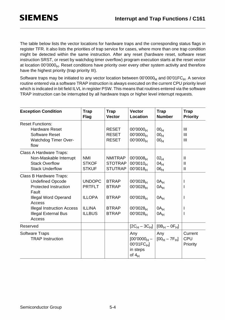
10Jul97@15:19h Interrupt and Trap Functions / C161
The table below lists the vector locations for hardware traps and the corresponding status flags inregister TFR. It also lists the priorities of trap service for cases, where more than one trap conditionmight be detected within the same instruction. After any reset (hardware reset, software resetinstruction SRST, or reset by watchdog timer overflow) program execution starts at the reset vectorat location 00’0000H. Reset conditions have priority over every other system activity and thereforehave the highest priority (trap priority III).
Software traps may be initiated to any vector location between 00’0000H and 00’01FCH. A serviceroutine entered via a software TRAP instruction is always executed on the current CPU priority levelwhich is indicated in bit field ILVL in register PSW. This means that routines entered via the softwareTRAP instruction can be interrupted by all hardware traps or higher level interrupt requests.
Exception Condition TrapFlag
TrapVector
VectorLocation
TrapNumber
TrapPriority
Reset Functions:Hardware ResetSoftware ResetWatchdog Timer Over-flow
RESETRESETRESET
00’0000H00’0000H00’0000H
00H00H00H
IIIIIIIII
Class A Hardware Traps:Non-Maskable InterruptStack OverflowStack Underflow
NMISTKOFSTKUF
NMITRAPSTOTRAPSTUTRAP
00’0008H00’0010H00’0018H
02H04H06H
IIIIII
Class B Hardware Traps:Undefined OpcodeProtected InstructionFaultIllegal Word OperandAccessIllegal Instruction AccessIllegal External BusAccess
UNDOPCPRTFLT
ILLOPA
ILLINAILLBUS
BTRAPBTRAP
BTRAP
BTRAPBTRAP
00’0028H00’0028H
00’0028H
00’0028H00’0028H
0AH0AH
0AH
0AH0AH
II
I
II
Reserved [2CH – 3CH] [0BH – 0FH]
Software TrapsTRAP Instruction
Any[00’0000H – 00’01FCH]in stepsof 4H
Any[00H – 7FH]
CurrentCPU Priority
Semiconductor Group 5-4
10Jul97@15:19h Interrupt and Trap Functions / C161
Normal Interrupt Processing and PEC Service
During each instruction cycle one out of all sources which require PEC or interrupt processing isselected according to its interrupt priority. This priority of interrupts and PEC requests isprogrammable in two levels. Each requesting source can be assigned to a specific priority. Asecond level (called “group priority”) allows to specify an internal order for simultaneous requestsfrom a group of different sources on the same priority level. At the end of each instruction cycle theone source request with the highest current priority will be determined by the interrupt system. Thisrequest will then be serviced, if its priority is higher than the current CPU priority in register PSW.
Interrupt System Register Description
Interrupt processing is controlled globally by register PSW through a general interrupt enable bit(IEN) and the CPU priority field (ILVL). Additionally the different interrupt sources are controlledindividually by their specific interrupt control registers (...IC). Thus, the acceptance of requests bythe CPU is determined by both the individual interrupt control registers and the PSW. PEC servicesare controlled by the respective PECCx register and the source and destination pointers, whichspecify the task of the respective PEC service channel.
Interrupt Control Registers
All interrupt control registers are organized identically. The lower 8 bits of an interrupt controlregister contain the complete interrupt status information of the associated source, which is requiredduring one round of prioritization, the upper 8 bits of the respective register are reserved.. Allinterrupt control registers are bit-addressable and all bits can be read or written via software. Thisallows each interrupt source to be programmed or modified with just one instruction. Whenaccessing interrupt control registers through instructions which operate on word data types, theirupper 8 bits (15...8) will return zeros, when read, and will discard written data.
The layout of the Interrupt Control registers shown below applies to each xxIC register, where xxstands for the mnemonic for the respective source.
Semiconductor Group 5-5
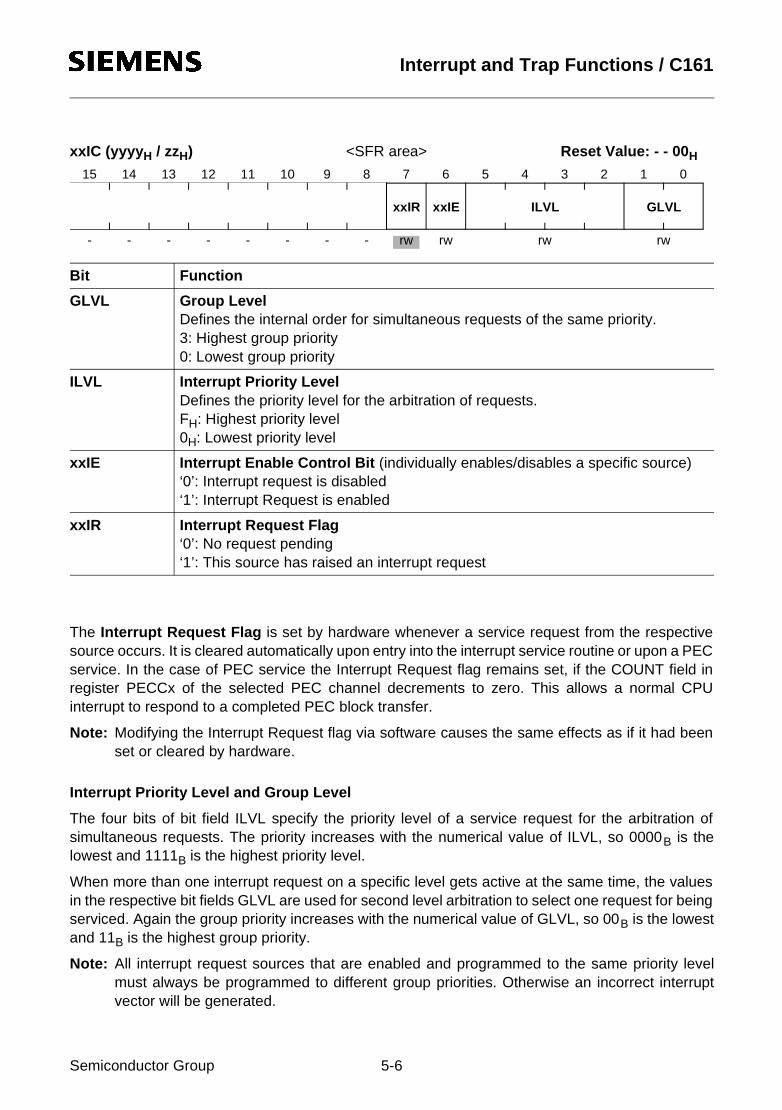
10Jul97@15:19h Interrupt and Trap Functions / C161
xxIC (yyyyH / zzH) <SFR area> Reset Value: - - 00H
The Interrupt Request Flag is set by hardware whenever a service request from the respectivesource occurs. It is cleared automatically upon entry into the interrupt service routine or upon a PECservice. In the case of PEC service the Interrupt Request flag remains set, if the COUNT field inregister PECCx of the selected PEC channel decrements to zero. This allows a normal CPUinterrupt to respond to a completed PEC block transfer.
Note: Modifying the Interrupt Request flag via software causes the same effects as if it had beenset or cleared by hardware.
Interrupt Priority Level and Group Level
The four bits of bit field ILVL specify the priority level of a service request for the arbitration ofsimultaneous requests. The priority increases with the numerical value of ILVL, so 0000B is thelowest and 1111B is the highest priority level.
When more than one interrupt request on a specific level gets active at the same time, the valuesin the respective bit fields GLVL are used for second level arbitration to select one request for beingserviced. Again the group priority increases with the numerical value of GLVL, so 00B is the lowestand 11B is the highest group priority.
Note: All interrupt request sources that are enabled and programmed to the same priority levelmust always be programmed to different group priorities. Otherwise an incorrect interruptvector will be generated.
Bit Function
GLVL Group LevelDefines the internal order for simultaneous requests of the same priority.3: Highest group priority0: Lowest group priority
ILVL Interrupt Priority LevelDefines the priority level for the arbitration of requests.FH: Highest priority level0H: Lowest priority level
xxIE Interrupt Enable Control Bit (individually enables/disables a specific source)‘0’: Interrupt request is disabled‘1’: Interrupt Request is enabled
xxIR Interrupt Request Flag‘0’: No request pending‘1’: This source has raised an interrupt request
5 4 3 2 1 011 10 9 8 7 615 14 13 12
rw rw- - - - rw rw- - - -
xxIExxIR GLVLILVL
Semiconductor Group 5-6

10Jul97@15:19h Interrupt and Trap Functions / C161
Upon entry into the interrupt service routine, the priority level of the source that won the arbitrationand who’s priority level is higher than the current CPU level, is copied into bit field ILVL of registerPSW after pushing the old PSW contents on the stack.
The interrupt system of the C161 allows nesting of up to 15 interrupt service routines of differentpriority levels (level 0 cannot be arbitrated).
Interrupt requests that are programmed to priority levels 15 or 14 (ie, ILVL=111XB) will be servicedby the PEC, unless the COUNT field of the associated PECC register contains zero. In this case therequest will instead be serviced by normal interrupt processing. Interrupt requests that areprogrammed to priority levels 13 through 1 will always be serviced by normal interrupt processing.
Note: Priority level 0000B is the default level of the CPU. Therefore a request on level 0 will neverbe serviced, because it can never interrupt the CPU. However, an enabled interrupt requeston level 0000B will terminate the C161’s Idle mode and reactivate the CPU.
For interrupt requests which are to be serviced by the PEC, the associated PEC channel number isderived from the respective ILVL (LSB) and GLVL (see figure below). So programming a source topriority level 15 (ILVL=1111B) selects the PEC channel group 7...4, programming a source topriority level 14 (ILVL=1110B) selects the PEC channel group 3...0. The actual PEC channelnumber is then determined by the group priority field GLVL.
Figure 5-1Priority Levels and PEC Channels
Simultaneous requests for PEC channels are prioritized according to the PEC channel number,where channel 0 has lowest and channel 8 has highest priority.
Note: All sources that request PEC service must be programmed to different PEC channels.Otherwise an incorrect PEC channel may be activated.
InterruptControl Register
PEC Control
Semiconductor Group 5-7

10Jul97@15:19h Interrupt and Trap Functions / C161
The table below shows in a few examples, which action is executed with a given programming of aninterrupt control register.
Note: All requests on levels 13...1 cannot initiate PEC transfers. They are always serviced by aninterrupt service routine. No PECC register is associated and no COUNT field is checked.
Interrupt Control Functions in the PSW
The Processor Status Word (PSW) is functionally divided into 2 parts: the lower byte of the PSWbasically represents the arithmetic status of the CPU, the upper byte of the PSW controls theinterrupt system of the C161 and the arbitration mechanism for the external bus interface.
Note: Pipeline effects have to be considered when enabling/disabling interrupt requests viamodifications of register PSW (see chapter “The Central Processing Unit”).
Priority Level Type of Service
ILVL GLVL COUNT = 00H COUNT ≠ 00H
1 1 1 1 1 1 CPU interrupt,level 15, group priority 3
PEC service,channel 7
1 1 1 1 1 0 CPU interrupt,level 15, group priority 2
PEC service,channel 6
1 1 1 0 1 0 CPU interrupt,level 14, group priority 2
PEC service,channel 2
1 1 0 1 1 0 CPU interrupt,level 13, group priority 2
CPU interrupt,level 13, group priority 2
0 0 0 1 1 1 CPU interrupt,level 1, group priority 3
CPU interrupt,level 1, group priority 3
0 0 0 1 0 0 CPU interrupt,level 1, group priority 0
CPU interrupt,level 1, group priority 0
0 0 0 0 X X No service! No service!
Semiconductor Group 5-8

10Jul97@15:19h Interrupt and Trap Functions / C161
PSW (FF10H / 88H) SFR Reset Value: 0000H
CPU Priority ILVL defines the current level for the operation of the CPU. This bit field reflects thepriority level of the routine that is currently executed. Upon the entry into an interrupt service routinethis bit field is updated with the priority level of the request that is being serviced. The PSW is savedon the system stack before. The CPU level determines the minimum interrupt priority level that willbe serviced. Any request on the same or a lower level will not be acknowledged.The current CPU priority level may be adjusted via software to control which interrupt requestsources will be acknowledged.
PEC transfers do not really interrupt the CPU, but rather “steal” a single cycle, so PEC services donot influence the ILVL field in the PSW.
Hardware traps switch the CPU level to maximum priority (ie. 15) so no interrupt or PEC requestswill be acknowledged while an exception trap service routine is executed.
Note: The TRAP instruction does not change the CPU level, so software invoked trap serviceroutines may be interrupted by higher requests.
Interrupt Enable bit IEN globally enables or disables PEC operation and the acceptance ofinterrupts by the CPU. When IEN is cleared, no interrupt requests are accepted by the CPU. WhenIEN is set to '1', all interrupt sources, which have been individually enabled by the interrupt enablebits in their associated control registers, are globally enabled.
Note: Traps are non-maskable and are therefore not affected by the IEN bit.
Bit Function
N, C, V, Z, E, MULIP, USR0
CPU status flags (Described in section “The Central Processing Unit”)Define the current status of the CPU (ALU, multiplication unit).
ILVL CPU Priority LevelDefines the current priority level for the CPUFH: Highest priority level0H: Lowest priority level
IEN Interrupt Enable Control Bit (globally enables/disables interrupt requests)‘0’: Interrupt requests are disabled‘1’: Interrupt requests are enabled
--MUL
IPUSR0 NZ CVE
5 4 3 2 1 011 10 9 8 7 615 14 13 12
rw rw rw rw- rw rw rw-rw --
IEN --ILVL
rw
Semiconductor Group 5-9

10Jul97@15:19h Interrupt and Trap Functions / C161
5.2 Operation of the PEC Channels
The C161’s Peripheral Event Controller (PEC) provides 8 PEC service channels, which move asingle byte or word between two locations in segment 0 (data pages 3...0). This is the fastestpossible interrupt response and in many cases is sufficient to service the respective peripheralrequest (eg. serial channels, etc.). Each channel is controlled by a dedicated PEC ChannelCounter/Control register (PECCx) and a pair of pointers for source (SRCPx) and destination(DSTPx) of the data transfer.
The PECC registers control the action that is performed by the respective PEC channel.
PECCx (FECyH / 6zH, see table) SFR Reset Value: 0000H
PEC Control Register Addresses
Byte/Word Transfer bit BWT controls, if a byte or a word is moved during a PEC service cycle.This selection controls the transferred data size and the increment step for the modified pointer.
Bit Function
COUNT PEC Transfer CountCounts PEC transfers and influences the channel’s action (see table below)
BWT Byte / Word Transfer Selection0: Transfer a Word1: Transfer a Byte
INC Increment Control (Modification of SRCPx or DSTPx)0 0: Pointers are not modified0 1: Increment DSTPx by 1 or 2 (BWT)1 0: Increment SRCPx by 1 or 2 (BWT)1 1: Reserved. Do not use this combination. (changed to 10 by hardware)
Register Address Reg. Space Register Address Reg. Space
PECC0 FEC0H / 60H SFR PECC4 FEC8H / 64H SFR
PECC1 FEC2H / 61H SFR PECC5 FECAH / 65H SFR
PECC2 FEC4H / 62H SFR PECC6 FECCH / 66H SFR
PECC3 FEC6H / 63H SFR PECC7 FECEH / 67H SFR
--
5 4 3 2 1 011 10 9 8 7 615 14 13 12
rwrwrw
- BWT
-----
-- INC COUNT
Semiconductor Group 5-10

10Jul97@15:19h Interrupt and Trap Functions / C161
Increment Control Field INC controls, if one of the PEC pointers is incremented after the PECtransfer. It is not possible to increment both pointers, however. If the pointers are not modified(INC=’00’), the respective channel will always move data from the same source to the samedestination.
Note: The reserved combination ‘11’ is changed to ‘10’ by hardware. However, it is notrecommended to use this combination.
The PEC Transfer Count Field COUNT controls the action of a respective PEC channel, where thecontent of bit field COUNT at the time the request is activated selects the action. COUNT may allowa specified number of PEC transfers, unlimited transfers or no PEC service at all.
The table below summarizes, how the COUNT field itself, the interrupt requests flag IR and the PECchannel action depends on the previous content of COUNT.
The PEC transfer counter allows to service a specified number of requests by the respective PECchannel, and then (when COUNT reaches 00H) activate the interrupt service routine, which isassociated with the priority level. After each PEC transfer the COUNT field is decremented and therequest flag is cleared to indicate that the request has been serviced.
Continuous transfers are selected by the value FFH in bit field COUNT. In this case COUNT is notmodified and the respective PEC channel services any request until it is disabled again.
When COUNT is decremented from 01H to 00H after a transfer, the request flag is not cleared,which generates another request from the same source. When COUNT already contains the value00H, the respective PEC channel remains idle and the associated interrupt service routine isactivated instead. This allows to choose, if a level 15 or 14 request is to be serviced by the PEC orby the interrupt service routine.
Note: PEC transfers are only executed, if their priority level is higher than the CPU level, ie. onlyPEC channels 7...4 are processed, while the CPU executes on level 14.All interrupt request sources that are enabled and programmed for PEC service should usedifferent channels. Otherwise only one transfer will be performed for all simultaneousrequests. When COUNT is decremented to 00H, and the CPU is to be interrupted, anincorrect interrupt vector will be generated.
Previous COUNT
Modified COUNT
IR after PEC service
Action of PEC Channeland Comments
FFH FFH ‘0’ Move a Byte / WordContinuous transfer mode, ie. COUNT is not modified
FEH..02H FDH..01H ‘0’ Move a Byte / Word and decrement COUNT
01H 00H ‘1’ Move a Byte / WordLeave request flag set, which triggers another request
00H 00H (‘1’) No action!Activate interrupt service routine rather than PEC channel.
Semiconductor Group 5-11
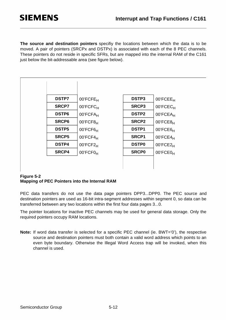
10Jul97@15:19h Interrupt and Trap Functions / C161
The source and destination pointers specifiy the locations between which the data is to bemoved. A pair of pointers (SRCPx and DSTPx) is associated with each of the 8 PEC channels.These pointers do not reside in specific SFRs, but are mapped into the internal RAM of the C161just below the bit-addressable area (see figure below).
Figure 5-2Mapping of PEC Pointers into the Internal RAM
PEC data transfers do not use the data page pointers DPP3...DPP0. The PEC source anddestination pointers are used as 16-bit intra-segment addresses within segment 0, so data can betransferred between any two locations within the first four data pages 3...0.
The pointer locations for inactive PEC channels may be used for general data storage. Only therequired pointers occupy RAM locations.
Note: If word data transfer is selected for a specific PEC channel (ie. BWT=’0’), the respectivesource and destination pointers must both contain a valid word address which points to aneven byte boundary. Otherwise the Illegal Word Access trap will be invoked, when thischannel is used.
DSTP7 00’FCFEH
SRCP7 00’FCFCH
DSTP6 00’FCFAH
SRCP6 00’FCF8H
DSTP5 00’FCF6H
SRCP5 00’FCF4H
DSTP4 00’FCF2H
SRCP4 00’FCF0H
DSTP3 00’FCEEH
SRCP3 00’FCECH
DSTP2 00’FCEAH
SRCP2 00’FCE8H
DSTP1 00’FCE6H
SRCP1 00’FCE4H
DSTP0 00’FCE2H
SRCP0 00’FCE0H
Semiconductor Group 5-12
10Jul97@15:19h Interrupt and Trap Functions / C161
5.3 Prioritization of Interrupt and PEC Service Requests
Interrupt and PEC service requests from all sources can be enabled, so they are arbitrated andserviced (if they win), or they may be disabled, so their requests are disregarded and not serviced.
Enabling and disabling interrupt requests may be done via three mechanisms:
Control Bits allow to switch each individual source “ON” or “OFF”, so it may generate a request ornot. The control bits (xxIE) are located in the respective interrupt control registers. All interruptrequests may be enabled or disabled generally via bit IEN in register PSW. This control bit is the“main switch” that selects, if requests from any source are accepted or not.For a specific request to be arbitrated the respective source’s enable bit and the global enable bitmust both be set.
The Priority Level automatically selects a certain group of interrupt requests that will beacknowledged, disclosing all other requests. The priority level of the source that won the arbitrationis compared against the CPU’s current level and the source is only serviced, if its level is higher thanthe current CPU level. Changing the CPU level to a specific value via software blocks all requestson the same or a lower level. An interrupt source that is assigned to level 0 will be disabled andnever be serviced.
The ATOMIC and EXTend instructions automatically disable all interrupt requests for the durationof the following 1...4 instructions. This is useful eg. for semaphore handling and does not require tore-enable the interrupt system after the unseparable instruction sequence (see chapter “SystemProgramming”).
Interrupt Class Management
An interrupt class covers a set of interrupt sources with the same importance, ie. the same priorityfrom the system’s viewpoint. Interrupts of the same class must not interrupt each other. The C161supports this function with two features:
Classes with up to 4 members can be established by using the same interrupt priority (ILVL) andassigning a dedicated group level (GLVL) to each member. This functionality is built-in and handledautomatically by the interrupt controller.
Classes with more than 4 members can be established by using a number of adjacent interruptpriorities (ILVL) and the respective group levels (4 per ILVL). Each interrupt service routine withinthis class sets the CPU level to the highest interrupt priority within the class. All requests from thesame or any lower level are blocked now, ie. no request of this class will be accepted.
The example below establishes 3 interrupt classes which cover 2 or 3 interrupt priorities, dependingon the number of members in a class. A level 6 interrupt disables all other sources in class 2 bychanging the current CPU level to 8, which is the highest priority (ILVL) in class 2. Class 1 requestsor PEC requests are still serviced in this case.
The 19 interrupt sources (excluding PEC requests) are so assigned to 3 classes of priority ratherthan to 7 different levels, as the hardware support would do.
Semiconductor Group 5-13
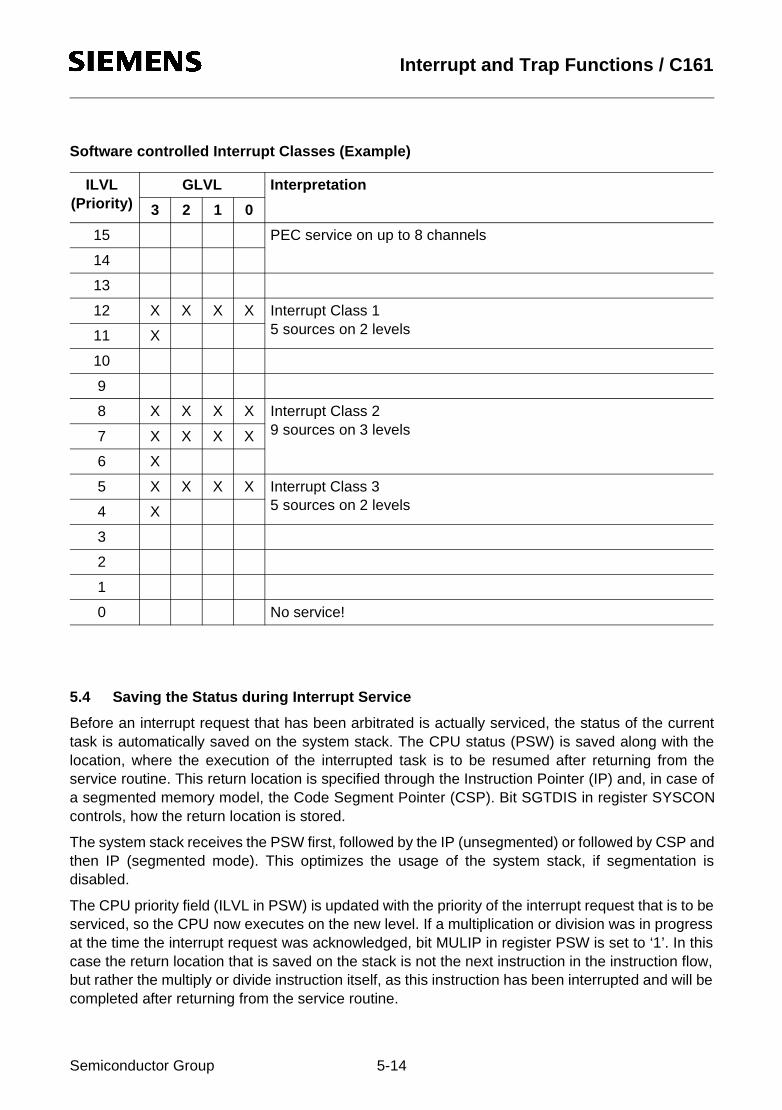
10Jul97@15:19h Interrupt and Trap Functions / C161
Software controlled Interrupt Classes (Example)
5.4 Saving the Status during Interrupt Service
Before an interrupt request that has been arbitrated is actually serviced, the status of the currenttask is automatically saved on the system stack. The CPU status (PSW) is saved along with thelocation, where the execution of the interrupted task is to be resumed after returning from theservice routine. This return location is specified through the Instruction Pointer (IP) and, in case ofa segmented memory model, the Code Segment Pointer (CSP). Bit SGTDIS in register SYSCONcontrols, how the return location is stored.
The system stack receives the PSW first, followed by the IP (unsegmented) or followed by CSP andthen IP (segmented mode). This optimizes the usage of the system stack, if segmentation isdisabled.
The CPU priority field (ILVL in PSW) is updated with the priority of the interrupt request that is to beserviced, so the CPU now executes on the new level. If a multiplication or division was in progressat the time the interrupt request was acknowledged, bit MULIP in register PSW is set to ‘1’. In thiscase the return location that is saved on the stack is not the next instruction in the instruction flow,but rather the multiply or divide instruction itself, as this instruction has been interrupted and will becompleted after returning from the service routine.
ILVL(Priority)
GLVL Interpretation
3 2 1 0
15 PEC service on up to 8 channels
14
13
12 X X X X Interrupt Class 15 sources on 2 levels11 X
10
9
8 X X X X Interrupt Class 29 sources on 3 levels7 X X X X
6 X
5 X X X X Interrupt Class 35 sources on 2 levels4 X
3
2
1
0 No service!
Semiconductor Group 5-14

10Jul97@15:19h Interrupt and Trap Functions / C161
Figure 5-3Task Status saved on the System Stack
The interrupt request flag of the source that is being serviced is cleared. The IP is loaded with thevector associated with the requesting source (the CSP is cleared in case of segmentation) and thefirst instruction of the service routine is fetched from the respective vector location, which isexpected to branch to the service routine itself. The data page pointers and the context pointer arenot affected.
When the interrupt service routine is left (RETI is executed), the status information is popped fromthe system stack in the reverse order, taking into account the value of bit SGTDIS.
Context Switching
An interrupt service routine usually saves all the registers it uses on the stack, and restores thembefore returning. The more registers a routine uses, the more time is wasted with saving andrestoring. The C161 allows to switch the complete bank of CPU registers (GPRs) with a singleinstruction, so the service routine executes within its own, separate context.
The instruction “SCXT CP, #New_Bank” pushes the content of the context pointer (CP) on thesystem stack and loads CP with the immediate value “New_Bank”, which selects a new registerbank. The service routine may now use its “own registers”. This register bank is preserved, whenthe service routine terminates, ie. its contents are available on the next call.Before returning (RETI) the previous CP is simply POPped from the system stack, which returns theregisters to the original bank.
Note: The first instruction following the SCXT instruction must not use a GPR.
Resources that are used by the interrupting program must eventually be saved and restored, eg. theDPPs and the registers of the MUL/DIV unit.
Semiconductor Group 5-15

10Jul97@15:19h Interrupt and Trap Functions / C161
5.5 Interrupt Response Times
The interrupt response time defines the time from an interrupt request flag of an enabled interruptsource being set until the first instruction (I1) being fetched from the interrupt vector location. Thebasic interrupt response time for the C161 is 3 instruction cycles.
Figure 5-4Pipeline Diagram for Interrupt Response Time
All instructions in the pipeline including instruction N (during which the interrupt request flag is set)are completed before entering the service routine. The actual execution time for these instructions(eg. waitstates) therefore influences the interrupt response time.
In the figure above the respective interrupt request flag is set in cycle 1 (fetching of instruction N).The indicated source wins the prioritization round (during cycle 2). In cycle 3 a TRAP instruction isinjected into the decode stage of the pipeline, replacing instruction N+1 and clearing the source’sinterrupt request flag to ’0’. Cycle 4 completes the injected TRAP instruction (save PSW, IP andCSP, if segmented mode) and fetches the first instruction (I1) from the respective vector location.
All instructions that entered the pipeline after setting of the interrupt request flag (N+1, N+2) will beexecuted after returning from the interrupt service routine.
The minimum interrupt response time is 5 states (250 ns @ 20 MHz CPU clock). This requiresprogram execution from the internal ROM, no external operand read requests and setting theinterrupt request flag during the last state of an instruction cycle. When the interrupt request flag isset during the first state of an instruction cycle, the minimum interrupt response time under theseconditions is 6 state times (300 ns @ 20 MHz CPU clock).
The interrupt response time is increased by all delays of the instructions in the pipeline that areexecuted before entering the service routine (including N).
Pipeline Stage Cycle 1 Cycle 2 Cycle 3 Cycle 4
FETCH N N + 1 N + 2 I1
DECODE N - 1 N TRAP (1) TRAP (2)
EXECUTE N - 2 N - 1 N TRAP
WRITEBACK N - 3 N - 2 N - 1 N
Interrupt Response Time
10
IR-Flag
Semiconductor Group 5-16

10Jul97@15:19h Interrupt and Trap Functions / C161
• When internal hold conditions between instruction pairs N-2/N-1 or N-1/N occur, or instruction Nexplicitly writes to the PSW or the SP, the minimum interrupt response time may be extended by 1state time for each of these conditions.
• When instruction N reads an operand from the internal ROM, or when N is a call, return, trap, orMOV Rn, [Rm+ #data16] instruction, the minimum interrupt response time may additionally beextended by 2 state times during internal ROM program execution.
• In case instruction N reads the PSW and instruction N-1 has an effect on the condition flags, theinterrupt response time may additionally be extended by 2 state times.
The worst case interrupt response time during internal ROM program execution adds to 12 statetimes (600 ns @ 20 MHz CPU clock).
Any reference to external locations increases the interrupt response time due to pipeline relatedaccess priorities. The following conditions have to be considered:
• Instruction fetch from an external location• Operand read from an external location• Result write-back to an external location
Depending on where the instructions, source and destination operands are located, there are anumber of combinations. Note, however, that only access conflicts contribute to the delay.
A few examples illustrate these delays:
• The worst case interrupt response time including external accesses will occur, when instructionsN, N+1 and N+2 are executed out of external memory, instructions N-1 and N require externaloperand read accesses, instructions N-3 through N write back external operands, and the interruptvector also points to an external location. In this case the interrupt response time is the time toperform 9 word bus accesses, because instruction I1 cannot be fetched via the external bus until allwrite, fetch and read requests of preceding instructions in the pipeline are terminated.
• When the above example has the interrupt vector pointing into the internal ROM, the interruptresponse time is 7 word bus accesses plus 2 states, because fetching of instruction I1 from internalROM can start earlier.
• When instructions N, N+1 and N+2 are executed out of external memory and the interrupt vectoralso points to an external location, but all operands for instructions N-3 through N are in internalmemory, then the interrupt response time is the time to perform 3 word bus accesses.
• When the above example has the interrupt vector pointing into the internal ROM, the interruptresponse time is 1 word bus access plus 4 states.
After an interrupt service routine has been terminated by executing the RETI instruction, and iffurther interrupts are pending, the next interrupt service routine will not be entered until at least twoinstruction cycles have been executed of the program that was interrupted. In most cases twoinstructions will be executed during this time. Only one instruction will typically be executed, if thefirst instruction following the RETI instruction is a branch instruction (without cache hit), or if it readsan operand from internal ROM, or if it is executed out of the internal RAM.
Note: A bus access in this context also includes delays caused by an external READY signal or bybus arbitration (HOLD mode).
Semiconductor Group 5-17
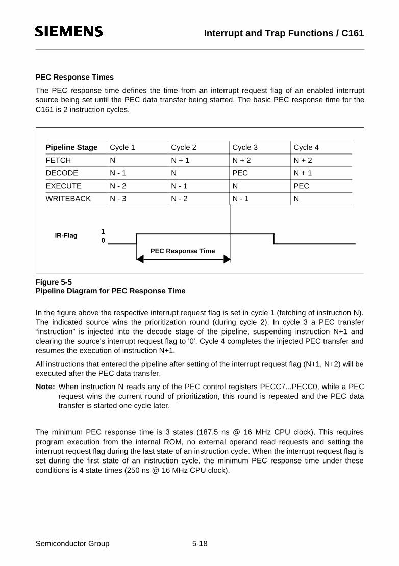
10Jul97@15:19h Interrupt and Trap Functions / C161
PEC Response Times
The PEC response time defines the time from an interrupt request flag of an enabled interruptsource being set until the PEC data transfer being started. The basic PEC response time for theC161 is 2 instruction cycles.
Figure 5-5Pipeline Diagram for PEC Response Time
In the figure above the respective interrupt request flag is set in cycle 1 (fetching of instruction N).The indicated source wins the prioritization round (during cycle 2). In cycle 3 a PEC transfer“instruction” is injected into the decode stage of the pipeline, suspending instruction N+1 andclearing the source's interrupt request flag to '0'. Cycle 4 completes the injected PEC transfer andresumes the execution of instruction N+1.
All instructions that entered the pipeline after setting of the interrupt request flag (N+1, N+2) will beexecuted after the PEC data transfer.
Note: When instruction N reads any of the PEC control registers PECC7...PECC0, while a PECrequest wins the current round of prioritization, this round is repeated and the PEC datatransfer is started one cycle later.
The minimum PEC response time is 3 states (187.5 ns @ 16 MHz CPU clock). This requiresprogram execution from the internal ROM, no external operand read requests and setting theinterrupt request flag during the last state of an instruction cycle. When the interrupt request flag isset during the first state of an instruction cycle, the minimum PEC response time under theseconditions is 4 state times (250 ns @ 16 MHz CPU clock).
Pipeline Stage Cycle 1 Cycle 2 Cycle 3 Cycle 4
FETCH N N + 1 N + 2 N + 2
DECODE N - 1 N PEC N + 1
EXECUTE N - 2 N - 1 N PEC
WRITEBACK N - 3 N - 2 N - 1 N
PEC Response Time
10
IR-Flag
Semiconductor Group 5-18
10Jul97@15:19h Interrupt and Trap Functions / C161
The PEC response time is increased by all delays of the instructions in the pipeline that areexecuted before starting the data transfer (including N).
• When internal hold conditions between instruction pairs N-2/N-1 or N-1/N occur, the minimumPEC response time may be extended by 1 state time for each of these conditions.
• When instruction N reads an operand from the internal ROM, or when N is a call, return, trap, orMOV Rn, [Rm+ #data16] instruction, the minimum PEC response time may additionally beextended by 2 state times during internal ROM program execution.
• In case instruction N reads the PSW and instruction N-1 has an effect on the condition flags, thePEC response time may additionally be extended by 2 state times.
The worst case PEC response time during internal ROM program execution adds to 9 state times(562.5 ns @ 16 MHz CPU clock).
Any reference to external locations increases the PEC response time due to pipeline related accesspriorities. The following conditions have to be considered:
• Instruction fetch from an external location• Operand read from an external location• Result write-back to an external location
Depending on where the instructions, source and destination operands are located, there are anumber of combinations. Note, however, that only access conflicts contribute to the delay.
A few examples illustrate these delays:
• The worst case interrupt response time including external accesses will occur, when instructionsN and N+1 are executed out of external memory, instructions N-1 and N require external operandread accesses and instructions N-3, N-2 and N-1 write back external operands. In this case the PECresponse time is the time to perform 7 word bus accesses.
• When instructions N and N+1 are executed out of external memory, but all operands forinstructions N-3 through N-1 are in internal memory, then the PEC response time is the time toperform 1 word bus access plus 2 state times.
Once a request for PEC service has been acknowledged by the CPU, the execution of the nextinstruction is delayed by 2 state times plus the additional time it might take to fetch the sourceoperand from internal ROM or external memory and to write the destination operand over theexternal bus in an external program environment.
Note: A bus access in this context also includes delays caused by an external READY signal or bybus arbitration (HOLD mode).
Semiconductor Group 5-19

10Jul97@15:19h Interrupt and Trap Functions / C161
5.6 External Interrupts
Although the C161 has no dedicated INTR input pins, it provides many possibilities to react onexternal asynchronous events by using a number of IO lines for interrupt input. The interruptfunction may either be combined with the pin’s main function or may be used instead of it, ie. if themain pin function is not required.
Interrupt signals may be connected to:
• T4IN, T2IN, the timer input pins,• CAPIN, the capture input of GPT2
For each of these pins either a positive, a negative, or both a positive and a negative externaltransition can be selected to cause an interrupt or PEC service request. The edge selection isperformed in the control register of the peripheral device associated with the respective port pin.The peripheral must be programmed to a specific operating mode to allow generation of an interruptby the external signal. The priority of the interrupt request is determined by the interrupt controlregister of the respective peripheral interrupt source, and the interrupt vector of this source will beused to service the external interrupt request.
Note: In order to use any of the listed pins as external interrupt input, it must be switched to inputmode via its direction control bit DPx.y in the respective port direction control register DPx.
Pins to be used as External Interrupt Inputs
Pins T2IN or T4IN can be used as external interrupt input pins when the associated auxiliary timerT2 or T4 in block GPT1 is configured for capture mode. This mode is selected by programming themode control fields T2M or T4M in control registers T2CON or T4CON to 101B. The active edge ofthe external input signal is determined by bit fields T2I or T4I. When these fields are programmedto X01B, interrupt request flags T2IR or T4IR in registers T2IC or T4IC will be set on a positiveexternal transition at pins T2IN or T4IN, respectively. When T2I or T4I are programmed to X10B,then a negative external transition will set the corresponding request flag. When T2I or T4I areprogrammed to X11B, both a positive and a negative transition will set the request flag. In all threecases, the contents of the core timer T3 will be captured into the auxiliary timer registers T2 or T4based on the transition at pins T2IN or T4IN. When the interrupt enable bits T2IE or T4IE are set,a PEC request or an interrupt request for vector T2INT or T4INT will be generated.
Pin CAPIN differs slightly from the timer input pins as it can be used as external interrupt input pinwithout affecting peripheral functions. When the capture mode enable bit T5SC in register T5CONis cleared to '0', signal transitions on pin CAPIN will only set the interrupt request flag CRIR inregister CRIC, and the capture function of register CAPREL is not activated.
Note: The GPT2 unit is only available on the C161O, not on the C161V and the C161K.
Port Pin Original Function Control Register
P3.7/T2IN Auxiliary timer T2 input pin T2CON
P3.5/T4IN Auxiliary timer T4 input pin T4CON
P3.2/CAPIN GPT2 capture input pin T5CON
Semiconductor Group 5-20

10Jul97@15:19h Interrupt and Trap Functions / C161
So register CAPREL can still be used as reload register for GPT2 timer T5, while pin CAPIN servesas external interrupt input. Bit field CI in register T5CON selects the effective transition of theexternal interrupt input signal. When CI is programmed to 01B, a positive external transition will setthe interrupt request flag. CI=10B selects a negative transition to set the interrupt request flag, andwith CI=11B, both a positive and a negative transition will set the request flag. When the interruptenable bit CRIE is set, an interrupt request for vector CRINT or a PEC request will be generated.
Note: The non-maskable interrupt input pin NMI and the reset input RSTIN provide anotherpossibility for the CPU to react on an external input signal. NMI and RSTIN are dedicatedinput pins, which cause hardware traps.
Fast External Interrupts
The input pins that may be used for external interrupts are sampled every 500 ns (@ 16 MHz CPUclock), ie. external events are scanned and detected in timeframes of 400 ns. The C161 provides 7interrupt inputs (4 on the C161V and C161K) that are sampled every 62.5 ns (@ 16 MHz CPUclock), so external events are captured faster than with standard interrupt inputs.
The pins of Port 2 (P2.15...P2.9) can individually be programmed to this fast interrupt mode, wherealso the trigger transition (rising, falling or both) can be selected. The External Interrupt Controlregister EXICON controls this feature for all 7 pins.
EXICON (F1C0H / E0H) ESFR Reset Value: 0000H
These fast external interrupt nodes and vectors are named according to the C167’s CAPCOMchannels CC15...CC9, so interrupt nodes receive equal names throughout the architecture. Seeregister description below.
Note: The fast external interrupt inputs are sampled every 62.5 ns. The interrupt request arbitrationand processing, however, is executed every 250 ns (both @ 16 MHz CPU clock).
Bit Function
EXIxES External Interrupt x Edge Selection Field (x=7...1)0 0: Fast external interrupts disabled: standard mode0 1: Interrupt on positive edge (rising)1 0: Interrupt on negative edge (falling)1 1: Interrupt on any edge (rising or falling)
--
5 4 3 2 1 011 10 9 8 7 615 14 13 12
-rwrw
EXI2ES EXI1ES
rwrwrw
EXI7ES EXI5ESEXI6ES
rwrw
EXI3ESEXI4ES
-
Semiconductor Group 5-21
10Jul97@15:19h Interrupt and Trap Functions / C161
The interrupt control registers listed below (CC15IC...CC9IC) control the fast external interrupts ofthe C161. They are named according to the C167’s CAPCOM channels, so interrupt nodes receiveequal names throughout the architecture.
CCxIC (See Table) SFR Reset Value: - - 00H
Note: Please refer to the general Interrupt Control Register description for an explanation of thecontrol fields.
Fast External Interrupt Control Register Addresses
Register Address External Interrupt
CC9IC FF8AH / C5H EX1IN
CC10IC FF8CH / C6H EX2IN
CC11IC FF8EH / C7H EX3IN
CC12IC FF90H / C8H EX4IN
CC13IC FF92H / C9H EX5IN
CC14IC FF94H / CAH EX6IN
CC15IC FF96H / CBH EX7IN
5 4 3 2 1 011 10 9 8 7 615 14 13 12
rw rw- - - - rw rw- - - -
CCxIE
CCxIR ILVL GLVL
Semiconductor Group 5-22
10Jul97@15:19h Interrupt and Trap Functions / C161
5.7 Trap Functions
Traps interrupt the current execution similar to standard interrupts. However, trap functions offer thepossibility to bypass the interrupt system’s prioritization process in cases where immediate systemreaction is required. Trap functions are not maskable and always have priority over interruptrequests on any priority level.
The C161 provides two different kinds of trapping mechanisms. Hardware traps are triggered byevents that occur during program execution (eg. illegal access or undefined opcode), softwaretraps are initiated via an instruction within the current execution flow.
Software Traps
The TRAP instruction is used to cause a software call to an interrupt service routine. The trapnumber that is specified in the operand field of the trap instruction determines which vector locationin the address range from 00’0000H through 00’01FCH will be branched to.
Executing a TRAP instruction causes a similar effect as if an interrupt at the same vector hadoccurred. PSW, CSP (in segmentation mode), and IP are pushed on the internal system stack anda jump is taken to the specified vector location. When segmentation is enabled and a trap isexecuted, the CSP for the trap service routine is set to code segment 0. No Interrupt Request flagsare affected by the TRAP instruction. The interrupt service routine called by a TRAP instructionmust be terminated with a RETI (return from interrupt) instruction to ensure correct operation.
Note: The CPU level in register PSW is not modified by the TRAP instruction, so the service routineis executed on the same priority level from which it was invoked. Therefore, the serviceroutine entered by the TRAP instruction can be interrupted by other traps or higher priorityinterrupts, other than when triggered by a hardware trap.
Hardware Traps
Hardware traps are issued by faults or specific system states that occur during runtime of a program(not identified at assembly time). A hardware trap may also be triggered intentionally, eg. to emulateadditional instructions by generating an Illegal Opcode trap. The C161 distinguishes eight differenthardware trap functions. When a hardware trap condition has been detected, the CPU branches tothe trap vector location for the respective trap condition. Depending on the trap condition, theinstruction which caused the trap is either completed or cancelled (ie. it has no effect on the systemstate) before the trap handling routine is entered.
Hardware traps are non-maskable and always have priority over every other CPU activity. If severalhardware trap conditions are detected within the same instruction cycle, the highest priority trap isserviced (see table in section “Interrupt System Structure”).
PSW, CSP (in segmentation mode), and IP are pushed on the internal system stack and the CPUlevel in register PSW is set to the highest possible priority level (ie. level 15), disabling all interrupts.The CSP is set to code segment zero, if segmentation is enabled. A trap service routine must beterminated with the RETI instruction.
Semiconductor Group 5-23

10Jul97@15:19h Interrupt and Trap Functions / C161
The eight hardware trap functions of the C161 are divided into two classes:
Class A traps are• external Non-Maskable Interrupt (NMI)• Stack Overflow• Stack Underflow trapThese traps share the same trap priority, but have an individual vector address.
Class B traps are• Undefined Opcode• Protection Fault• Illegal Word Operand Access• Illegal Instruction Access• Illegal External Bus Access TrapThese traps share the same trap priority, and the same vector address.
The bit-addressable Trap Flag Register (TFR) allows a trap service routine to identify the kind oftrap which caused the exception. Each trap function is indicated by a separate request flag. Whena hardware trap occurs, the corresponding request flag in register TFR is set to '1'.
TFR (FFACH / D6H) SFR Reset Value: 0000H
Bit Function
ILLBUS Illegal External Bus Access FlagAn external access has been attempted with no external bus defined.
ILLINA Illegal Instruction Access FlagA branch to an odd address has been attempted.
ILLOPA Illegal Word Operand Access FlagA word operand access (read or write) to an odd address has been attempted.
PRTFLT Protection Fault FlagA protected instruction with an illegal format has been detected.
UNDOPC Undefined Opcode FlagThe currently decoded instruction has no valid C161 opcode.
STKUF Stack Underflow FlagThe current stack pointer value exceeds the content of register STKUN.
STKOF Stack Overflow FlagThe current stack pointer value falls below the content of register STKOV.
NMI Non Maskable Interrupt FlagA negative transition (falling edge) has been detected on pin NMI.
NMI
5 4 3 2 1 011 10 9 8 7 615 14 13 12
rw rw rw rwrw - - --rw ---
STKUF
ILLBUS
ILLINA
ILLOPA
PRTFLT
UNDOPC
STKOF - - - - - - --
-rwrw
Semiconductor Group 5-24
10Jul97@15:19h Interrupt and Trap Functions / C161
Note: The trap service routine must clear the respective trap flag, otherwise a new trap will berequested after exiting the service routine. Setting a trap request flag by software causes thesame effects as if it had been set by hardware.
The reset functions (hardware, software, watchdog) may be regarded as a type of trap. Resetfunctions have the highest system priority (trap priority III).
Class A traps have the second highest priority (trap priority II), on the 3rd rank are class B traps, soa class A trap can interrupt a class B trap. If more than one class A trap occur at a time, they areprioritized internally, with the NMI trap on the highest and the stack underflow trap on the lowestpriority.
All class B traps have the same trap priority (trap priority I). When several class B traps get activeat a time, the corresponding flags in the TFR register are set and the trap service routine is entered.Since all class B traps have the same vector, the priority of service of simultaneously occurring classB traps is determined by software in the trap service routine.
A class A trap occurring during the execution of a class B trap service routine will be servicedimmediately. During the execution of a class A trap service routine, however, any class B trapoccurring will not be serviced until the class A trap service routine is exited with a RETI instruction.In this case, the occurrence of the class B trap condition is stored in the TFR register, but the IPvalue of the instruction which caused this trap is lost.
In the case where e.g. an Undefined Opcode trap (class B) occurs simultaneously with an NMI trap(class A), both the NMI and the UNDOPC flag is set, the IP of the instruction with the undefinedopcode is pushed onto the system stack, but the NMI trap is executed. After return from the NMIservice routine, the IP is popped from the stack and immediately pushed again because of thepending UNDOPC trap.
External NMI Trap
Whenever a high to low transition on the dedicated external NMI pin (Non-Maskable Interrupt) isdetected, the NMI flag in register TFR is set and the CPU will enter the NMI trap routine. The IPvalue pushed on the system stack is the address of the instruction following the one after whichnormal processing was interrupted by the NMI trap.
Stack Overflow Trap
Whenever the stack pointer is decremented to a value which is less than the value in the stackoverflow register STKOV, the STKOF flag in register TFR is set and the CPU will enter the stackoverflow trap routine. Which IP value will be pushed onto the system stack depends on whichoperation caused the decrement of the SP. When an implicit decrement of the SP is made througha PUSH or CALL instruction, or upon interrupt or trap entry, the IP value pushed is the address ofthe following instruction. When the SP is decremented by a subtract instruction, the IP value pushedrepresents the address of the instruction after the instruction following the subtract instruction.
For recovery from stack overflow it must be ensured that there is enough excess space on the stackfor saving the current system state (PSW, IP, in segmented mode also CSP) twice. Otherwise, asystem reset should be generated.
Semiconductor Group 5-25

10Jul97@15:19h Interrupt and Trap Functions / C161
Stack Underflow Trap
Whenever the stack pointer is incremented to a value which is greater than the value in the stackunderflow register STKUN, the STKUF flag is set in register TFR and the CPU will enter the stackunderflow trap routine. Again, which IP value will be pushed onto the system stack depends onwhich operation caused the increment of the SP. When an implicit increment of the SP is madethrough a POP or return instruction, the IP value pushed is the address of the following instruction.When the SP is incremented by an add instruction, the pushed IP value represents the address ofthe instruction after the instruction following the add instruction.
Undefined Opcode Trap
When the instruction currently decoded by the CPU does not contain a valid C161 opcode, theUNDOPC flag is set in register TFR and the CPU enters the undefined opcode trap routine. The IPvalue pushed onto the system stack is the address of the instruction that caused the trap.
This can be used to emulate unimplemented instructions. The trap service routine can examine thefaulting instruction to decode operands for unimplemented opcodes based on the stacked IP. Inorder to resume processing, the stacked IP value must be incremented by the size of the undefinedinstruction, which is determined by the user, before a RETI instruction is executed.
Protection Fault Trap
Whenever one of the special protected instructions is executed where the opcode of that instructionis not repeated twice in the second word of the instruction and the byte following the opcode is notthe complement of the opcode, the PRTFLT flag in register TFR is set and the CPU enters theprotection fault trap routine. The protected instructions include DISWDT, EINIT, IDLE, PWRDN,SRST, and SRVWDT. The IP value pushed onto the system stack for the protection fault trap is theaddress of the instruction that caused the trap.
Illegal Word Operand Access Trap
Whenever a word operand read or write access is attempted to an odd byte address, the ILLOPAflag in register TFR is set and the CPU enters the illegal word operand access trap routine. The IPvalue pushed onto the system stack is the address of the instruction following the one which causedthe trap.
Illegal Instruction Access Trap
Whenever a branch is made to an odd byte address, the ILLINA flag in register TFR is set and theCPU enters the illegal instruction access trap routine. The IP value pushed onto the system stackis the illegal odd target address of the branch instruction.
Illegal External Bus Access Trap
Whenever the CPU requests an external instruction fetch, data read or data write, and no externalbus configuration has been specified, the ILLBUS flag in register TFR is set and the CPU enters theillegal bus access trap routine. The IP value pushed onto the system stack is the address of theinstruction following the one which caused the trap.
Semiconductor Group 5-26

10Jul97@15:19h Parallel Ports / C161
6 Parallel Ports
In order to accept or generate single external control signals or parallel data, the C161 provides upto 63 parallel IO lines organized into six IO ports and one input port:PORT0 made of P0H and P0L (8-bit), PORT1 made of P1H and P1L (8-bit), Port 2 (7-bit), Port 4(6-bit), Port 6 (4-bit), Port 3 (12-bit) and Port 5 (2-bit).
These port lines may be used for general purpose Input/Output controlled via software or may beused implicitly by the C161’s integrated peripherals or the External Bus Controller.
All port lines are bit addressable, and all input/output lines are individually (bit-wise) programmableas inputs or outputs via direction registers (except Port 5, of course). The IO ports are truebidirectional ports which are switched to high impedance state when configured as inputs. Theoutput drivers of three IO ports (2, 3, 6) can be configured (pin by pin) for push/pull operation oropen-drain operation via control registers. The logic level of a pin is clocked into the input latch onceper state time, regardless whether the port is configured for input or output.
A write operation to a port pin configured as an input causes the value to be written into the portoutput latch, while a read operation returns the latched state of the pin itself. A read-modify-writeoperation reads the value of the pin, modifies it, and writes it back to the output latch.
Writing to a pin configured as an output (DPx.y=‘1’) causes the output latch and the pin to have thewritten value, since the output buffer is enabled. Reading this pin returns the value of the outputlatch. A read-modify-write operation reads the value of the output latch, modifies it, and writes itback to the output latch, thus also modifying the level at the pin.
Figure 6-1SFRs and Pins associated with the Parallel Ports
ODP2 EDP2
P5
P2
Data Input / Output Registers
Direction Control Registers
Open Drain Control Registers
P6 DP6 ODP6 E
P0L
P0H
DP0L E
DP0H E
P4
P1L
P1H
P3 DP3
DP4
DP1H E
DP1L E
ODP3 E
Semiconductor Group 6-1

10Jul97@15:19h Parallel Ports / C161
In the C161 certain ports provide Open Drain Control, which allows to switch the output driver of aport pin from a push/pull configuration to an open drain configuration. In push/pull mode a portoutput driver has an upper and a lower transistor, thus it can actively drive the line either to a highor a low level. In open drain mode the upper transistor is always switched off, and the output drivercan only actively drive the line to a low level. When writing a ‘1’ to the port latch, the lower transistoris switched off and the output enters a high-impedance state. The high level must then be providedby an external pullup device. With this feature, it is possible to connect several port pins together toa Wired-AND configuration, saving external glue logic and/or additional software overhead forenabling/disabling output signals.
This feature is implemented for ports P2, P3 and P6 (see respective sections), and is controlledthrough the respective Open Drain Control Registers ODPx. These registers allow the individual bit-wise selection of the open drain mode for each port line. If the respective control bit ODPx.y is ‘0’(default after reset), the output driver is in the push/pull mode. If ODPx.y is ‘1’, the open drainconfiguration is selected. Note that all ODPx registers are located in the ESFR space.
Figure 6-2Output Drivers in Push/Pull Mode and in Open Drain Mode
Alternate Port Functions
Each port line has one programmable alternate input or output function associated with it.
PORT0 and PORT1 may be used as the address and data lines when accessing external memory.
Port 4 outputs the additional segment address bits A21/19/17...A16 in systems where more than64 KBytes of memory are to be accessed directly.
Port 6 provides the optional chip select outputs.
Port 2 is used for fast external interrupt inputs.
Port 3 includes alternate input/output functions of timers, serial interfaces and the optional buscontrol signal BHE/WRH.
Port 5 is used for timer control signals.
Semiconductor Group 6-2
10Jul97@15:19h Parallel Ports / C161
If an alternate output function of a pin is to be used, the direction of this pin must be programmedfor output (DPx.y=‘1’), except for some signals that are used directly after reset and are configuredautomatically. Otherwise the pin remains in the high-impedance state and is not effected by thealternate output function. The respective port latch should hold a ‘1’, because its output is ANDedwith the alternate output data.
If an alternate input function of a pin is used, the direction of the pin must be programmed for input(DPx.y=‘0’) if an external device is driving the pin. The input direction is the default after reset. If noexternal device is connected to the pin, however, one can also set the direction for this pin to output.In this case, the pin reflects the state of the port output latch. Thus, the alternate input function readsthe value stored in the port output latch. This can be used for testing purposes to allow a softwaretrigger of an alternate input function by writing to the port output latch.
On most of the port lines, the user software is responsible for setting the proper direction when usingan alternate input or output function of a pin. This is done by setting or clearing the direction controlbit DPx.y of the pin before enabling the alternate function. There are port lines, however, where thedirection of the port line is switched automatically. For instance, in the multiplexed external busmodes of PORT0, the direction must be switched several times for an instruction fetch in order tooutput the addresses and to input the data. Obviously, this cannot be done through instructions. Inthese cases, the direction of the port line is switched automatically by hardware if the alternatefunction of such a pin is enabled.To determine the appropriate level of the port output latches check how the alternate data output iscombined with the respective port latch output.
There is one basic structure for all port lines with only an alternate input function. Port lines with onlyan alternate output function, however, have different structures due to the way the direction of thepin is switched and depending on whether the pin is accessible by the user software or not in thealternate function mode.
All port lines that are not used for these alternate functions may be used as general purpose IOlines. When using port pins for general purpose output, the initial output value should be written tothe port latch prior to enabling the output drivers, in order to avoid undesired transitions on theoutput pins. This applies to single pins as well as to pin groups (see examples below).
SINGLE_BIT: BSET P4.7 ; Initial output level is “high”BSET DP4.7 ; Switch on the output driver
BIT_GROUP: BFLDH P4, #24H, #24H ; Initial output level is “high”BFLDH DP4, #24H, #24H ; Switch on the output drivers
Note: When using several BSET pairs to control more pins of one port, these pairs must beseparated by instructions, which do not reference the respective port (see “ParticularPipeline Effects” in chapter “The Central Processing Unit”).
Each of these ports and the alternate input and output functions are described in detail in thefollowing subsections.
Semiconductor Group 6-3
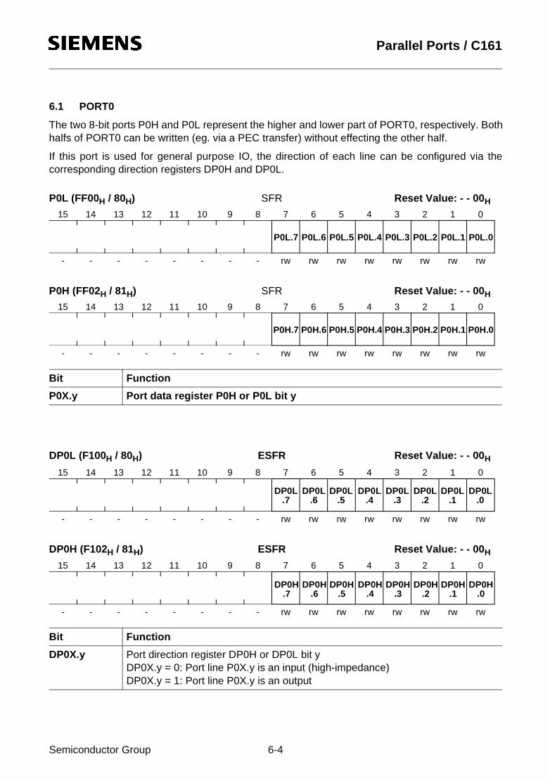
10Jul97@15:19h Parallel Ports / C161
6.1 PORT0
The two 8-bit ports P0H and P0L represent the higher and lower part of PORT0, respectively. Bothhalfs of PORT0 can be written (eg. via a PEC transfer) without effecting the other half.
If this port is used for general purpose IO, the direction of each line can be configured via thecorresponding direction registers DP0H and DP0L.
P0L (FF00H / 80H) SFR Reset Value: - - 00H
P0H (FF02H / 81H) SFR Reset Value: - - 00H
DP0L (F100H / 80H) ESFR Reset Value: - - 00H
DP0H (F102H / 81H) ESFR Reset Value: - - 00H
Bit Function
P0X.y Port data register P0H or P0L bit y
Bit Function
DP0X.y Port direction register DP0H or DP0L bit yDP0X.y = 0: Port line P0X.y is an input (high-impedance)DP0X.y = 1: Port line P0X.y is an output
5 4 3 2 1 011 10 9 8 7 615 14 13 12
rw rw rw rw rw rw- - - - rw rw- - - -
P0L.0P0L.1P0L.2P0L.3P0L.4P0L.5P0L.6P0L.7
5 4 3 2 1 011 10 9 8 7 615 14 13 12
rw rw rw rw rw rw- - - - rw rw- - - -
P0H.0P0H.1P0H.2P0H.3P0H.4P0H.5P0H.6P0H.7
DP0L.0
5 4 3 2 1 011 10 9 8 7 615 14 13 12
rw rw rw rw rw rw- - - - rw rw- - - -
DP0L.7
DP0L.6
DP0L.5
DP0L.4
DP0L.3
DP0L.2
DP0L.1
5 4 3 2 1 011 10 9 8 7 615 14 13 12
rw rw rw rw rw rw- - - - rw rw- - - -
DP0H.7
DP0H.6
DP0H.5
DP0H.4
DP0H.3
DP0H.2
DP0H.1
DP0H.0
Semiconductor Group 6-4
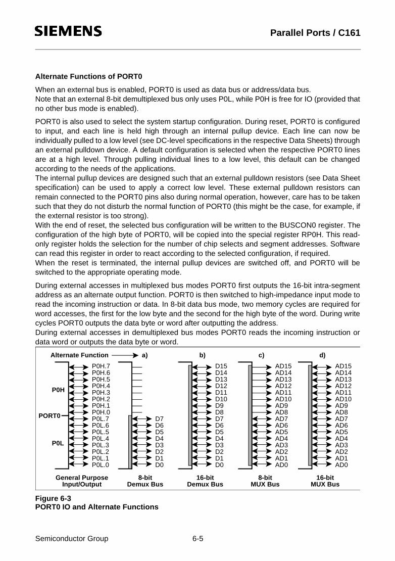
10Jul97@15:19h Parallel Ports / C161
Alternate Functions of PORT0
When an external bus is enabled, PORT0 is used as data bus or address/data bus.Note that an external 8-bit demultiplexed bus only uses P0L, while P0H is free for IO (provided thatno other bus mode is enabled).
PORT0 is also used to select the system startup configuration. During reset, PORT0 is configuredto input, and each line is held high through an internal pullup device. Each line can now beindividually pulled to a low level (see DC-level specifications in the respective Data Sheets) throughan external pulldown device. A default configuration is selected when the respective PORT0 linesare at a high level. Through pulling individual lines to a low level, this default can be changedaccording to the needs of the applications.The internal pullup devices are designed such that an external pulldown resistors (see Data Sheetspecification) can be used to apply a correct low level. These external pulldown resistors canremain connected to the PORT0 pins also during normal operation, however, care has to be takensuch that they do not disturb the normal function of PORT0 (this might be the case, for example, ifthe external resistor is too strong).With the end of reset, the selected bus configuration will be written to the BUSCON0 register. Theconfiguration of the high byte of PORT0, will be copied into the special register RP0H. This read-only register holds the selection for the number of chip selects and segment addresses. Softwarecan read this register in order to react according to the selected configuration, if required.When the reset is terminated, the internal pullup devices are switched off, and PORT0 will beswitched to the appropriate operating mode.
During external accesses in multiplexed bus modes PORT0 first outputs the 16-bit intra-segmentaddress as an alternate output function. PORT0 is then switched to high-impedance input mode toread the incoming instruction or data. In 8-bit data bus mode, two memory cycles are required forword accesses, the first for the low byte and the second for the high byte of the word. During writecycles PORT0 outputs the data byte or word after outputting the address.During external accesses in demultiplexed bus modes PORT0 reads the incoming instruction ordata word or outputs the data byte or word.
Figure 6-3PORT0 IO and Alternate Functions
P0H.7P0H.6P0H.5P0H.4P0H.3P0H.2P0H.1P0H.0P0L.7P0L.6P0L.5P0L.4P0L.3P0L.2P0L.1P0L.0
PORT0 D7D6D5D4D3D2D1D0
P0H
P0L
D15D14D13D12D11D10D9D8D7D6D5D4D3D2D1D0
AD15AD14AD13AD12AD11AD10AD9AD8AD7AD6AD5AD4AD3AD2AD1AD0
AD15AD14AD13AD12AD11AD10AD9AD8AD7AD6AD5AD4AD3AD2AD1AD0
Alternate Function a) b) c) d)
General PurposeInput/Output
8-bitDemux Bus
16-bitDemux Bus
8-bitMUX Bus
16-bitMUX Bus
Semiconductor Group 6-5

10Jul97@15:19h Parallel Ports / C161
When an external bus mode is enabled, the direction of the port pin and the loading of data into theport output latch are controlled by the bus controller hardware. The input of the port output latch isdisconnected from the internal bus and is switched to the line labeled “Alternate Data Output” via amultiplexer. The alternate data can be the 16-bit intrasegment address or the 8/16-bit datainformation. The incoming data on PORT0 is read on the line “Alternate Data Input”. While anexternal bus mode is enabled, the user software should not write to the port output latch, otherwiseunpredictable results may occur. When the external bus modes are disabled, the contents of thedirection register last written by the user becomes active.
The figure below shows the structure of a PORT0 pin.
Figure 6-4Block Diagram of a PORT0 Pin
y = 7...0
Semiconductor Group 6-6

10Jul97@15:19h Parallel Ports / C161
6.2 PORT1
The two 8-bit ports P1H and P1L represent the higher and lower part of PORT1, respectively. Bothhalfs of PORT1 can be written (eg. via a PEC transfer) without effecting the other half.
If this port is used for general purpose IO, the direction of each line can be configured via thecorresponding direction registers DP1H and DP1L.
P1L (FF04H / 82H) SFR Reset Value: - - 00H
P1H (FF06H / 83H) SFR Reset Value: - - 00H
DP1L (F104H / 82H) ESFR Reset Value: - - 00H
DP1H (F106H / 83H) ESFR Reset Value: - - 00H
Bit Function
P1X.y Port data register P1H or P1L bit y
Bit Function
DP1X.y Port direction register DP1H or DP1L bit yDP1X.y = 0: Port line P1X.y is an input (high-impedance)DP1X.y = 1: Port line P1X.y is an output
5 4 3 2 1 011 10 9 8 7 615 14 13 12
rw rw rw rw rw rw- - - - rw rw- - - -
P1L.0P1L.1P1L.2P1L.3P1L.4P1L.5P1L.6P1L.7
5 4 3 2 1 011 10 9 8 7 615 14 13 12
rw rw rw rw rw rw- - - - rw rw- - - -
P1H.0P1H.1P1H.2P1H.3P1H.4P1H.5P1H.6P1H.7
5 4 3 2 1 011 10 9 8 7 615 14 13 12
rw rw rw rw rw rw- - - - rw rw- - - -
DP1L.7
DP1L.6
DP1L.5
DP1L.4
DP1L.3
DP1L.2
DP1L.1
DP1L.0
5 4 3 2 1 011 10 9 8 7 615 14 13 12
rw rw rw rw rw rw- - - - rw rw- - - -
DP1H.7
DP1H.6
DP1H.5
DP1H.4
DP1H.3
DP1H.2
DP1H.1
DP1H.0
Semiconductor Group 6-7

10Jul97@15:19h Parallel Ports / C161
Alternate Functions of PORT1
When a demultiplexed external bus is enabled, PORT1 is used as address bus.Note that demultiplexed bus modes use PORT1 as a 16-bit port. Otherwise all 16 port lines can beused for general purpose IO.
During external accesses in demultiplexed bus modes PORT1 outputs the 16-bit intra-segmentaddress as an alternate output function.
During external accesses in multiplexed bus modes, when no BUSCON register selects ademultiplexed bus mode, PORT1 is not used and is available for general purpose IO.
Figure 6-5PORT1 IO and Alternate Functions
Note: Demultiplexed bus modes are only available on the C161K and C161O.
When an external bus mode is enabled, the direction of the port pin and the loading of data into theport output latch are controlled by the bus controller hardware. The input of the port output latch isdisconnected from the internal bus and is switched to the line labeled “Alternate Data Output” via amultiplexer. The alternate data is the 16-bit intrasegment address. While an external bus mode isenabled, the user software should not write to the port output latch, otherwise unpredictable resultsmay occur. When the external bus modes are disabled, the contents of the direction register lastwritten by the user becomes active.
P1H.7P1H.6P1H.5P1H.4P1H.3P1H.2P1H.1P1H.0P1L.7P1L.6P1L.5P1L.4P1L.3P1L.2P1L.1P1L.0
PORT1
P1H
P1L
A15A14A13A12A11A10A9A8A7A6A5A4A3A2A1A0
Alternate Function a)
General PurposeInput/Output
8/16-bitDemux Bus
Semiconductor Group 6-8
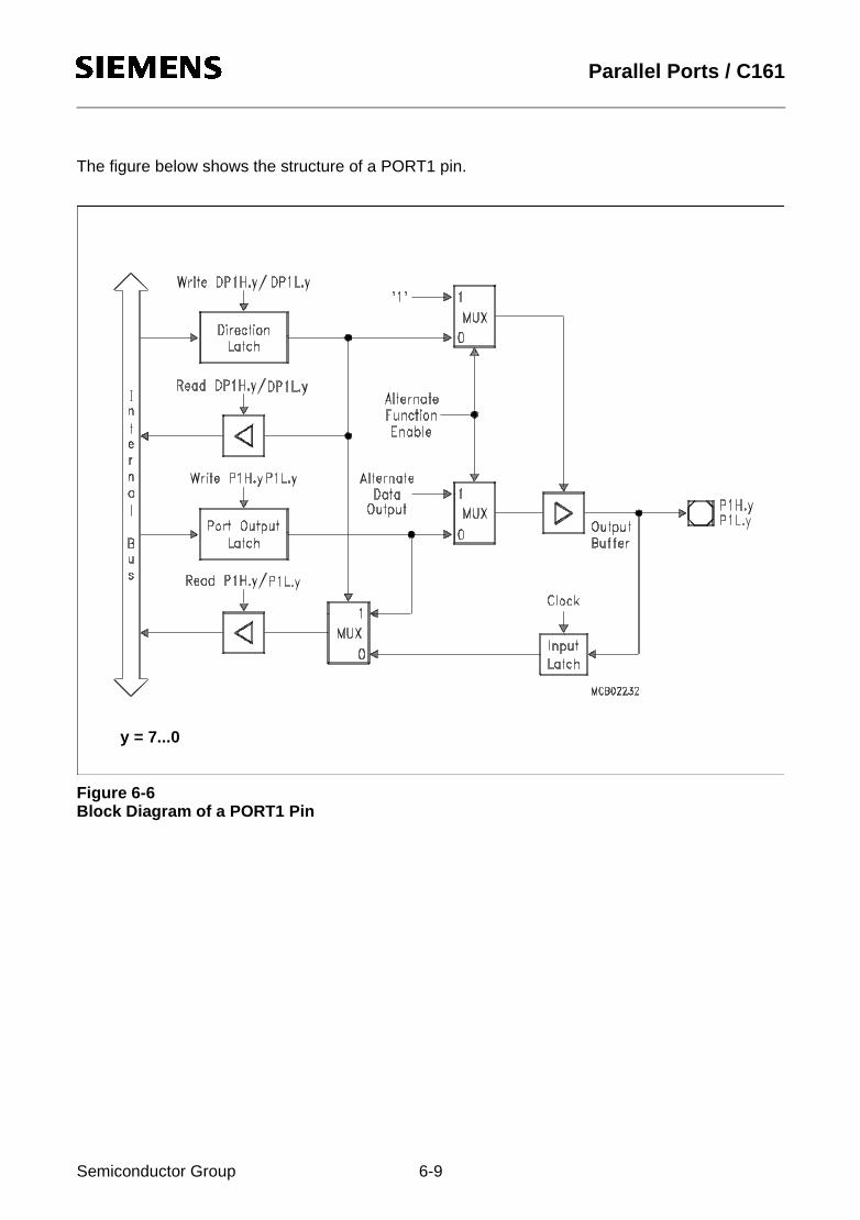
10Jul97@15:19h Parallel Ports / C161
The figure below shows the structure of a PORT1 pin.
Figure 6-6Block Diagram of a PORT1 Pin
y = 7...0
Semiconductor Group 6-9
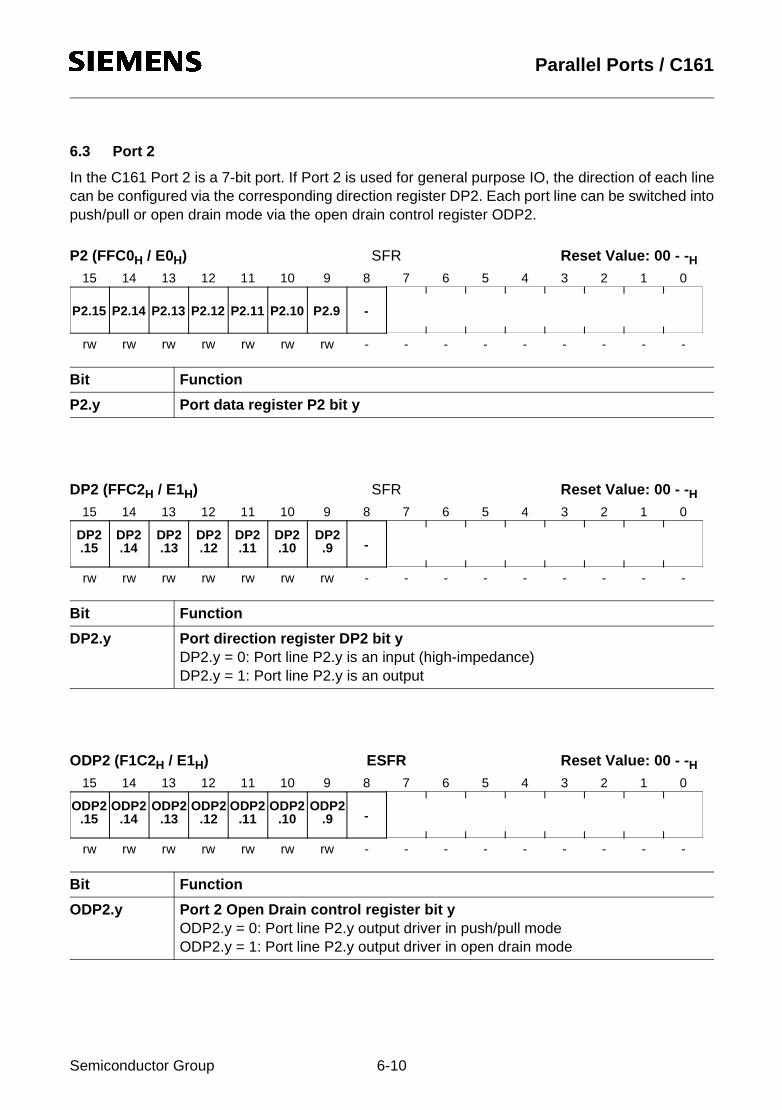
10Jul97@15:19h Parallel Ports / C161
6.3 Port 2
In the C161 Port 2 is a 7-bit port. If Port 2 is used for general purpose IO, the direction of each linecan be configured via the corresponding direction register DP2. Each port line can be switched intopush/pull or open drain mode via the open drain control register ODP2.
P2 (FFC0H / E0H) SFR Reset Value: 00 - -H
DP2 (FFC2H / E1H) SFR Reset Value: 00 - -H
ODP2 (F1C2H / E1H) ESFR Reset Value: 00 - -H
Bit Function
P2.y Port data register P2 bit y
Bit Function
DP2.y Port direction register DP2 bit yDP2.y = 0: Port line P2.y is an input (high-impedance)DP2.y = 1: Port line P2.y is an output
Bit Function
ODP2.y Port 2 Open Drain control register bit yODP2.y = 0: Port line P2.y output driver in push/pull modeODP2.y = 1: Port line P2.y output driver in open drain mode
5 4 3 2 1 011 10 9 8 7 615 14 13 12
- - - - - -rw rw rw - - -rw rw rw rw
-P2.9P2.10P2.11P2.12P2.13P2.14P2.15
5 4 3 2 1 011 10 9 8 7 615 14 13 12
- - - - - -rw rw rw - - -rw rw rw rw
DP2.15
DP2.14
DP2.13
DP2.12
DP2.11
DP2.10
DP2.9 -
ODP2.9 -
5 4 3 2 1 011 10 9 8 7 615 14 13 12
- - - - - -rw rw rw - - -rw rw rw rw
ODP2.15
ODP2.14
ODP2.13
ODP2.12
ODP2.11
ODP2.10
Semiconductor Group 6-10

10Jul97@15:19h Parallel Ports / C161
Alternate Functions of Port 2
All Port 2 lines (P2.15...P2.9) can serve as Fast External Interrupt inputs (EX7IN...EX1IN).
Note: EX7IN...EX5IN on P2.15...P2.13 are only available on the C161O.
The table below summarizes the alternate functions of Port 2.
Figure 6-7Port 2 IO and Alternate Functions
Port 2 Pin Alternate Function
P2.9P2.10P2.11P2.12
EX1IN Fast External Interrupt 1 InputEX2IN Fast External Interrupt 2 InputEX3IN Fast External Interrupt 3 InputEX4IN Fast External Interrupt 4 Input
P2.13P2.14P2.15
EX5IN Fast External Interrupt 5 InputEX6IN Fast External Interrupt 6 InputEX7IN Fast External Interrupt 7 Input
P2.15P2.14P2.13P2.12P2.11P2.10P2.9---------
Port 2
EX7INEX6INEX5INEX4INEX3INEX2INEX1IN---------
Alternate Function a)
General PurposeInput/Output
Fast ExternalInterrupt Input
Semiconductor Group 6-11

10Jul97@15:19h Parallel Ports / C161
Figure 6-8Block Diagram of a Port 2 Pin
y = 15...8
Semiconductor Group 6-12
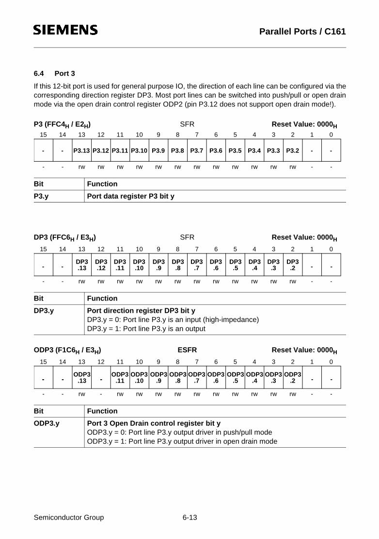
10Jul97@15:19h Parallel Ports / C161
6.4 Port 3
If this 12-bit port is used for general purpose IO, the direction of each line can be configured via thecorresponding direction register DP3. Most port lines can be switched into push/pull or open drainmode via the open drain control register ODP2 (pin P3.12 does not support open drain mode!).
P3 (FFC4H / E2H) SFR Reset Value: 0000H
DP3 (FFC6H / E3H) SFR Reset Value: 0000H
ODP3 (F1C6H / E3H) ESFR Reset Value: 0000H
Bit Function
P3.y Port data register P3 bit y
Bit Function
DP3.y Port direction register DP3 bit yDP3.y = 0: Port line P3.y is an input (high-impedance)DP3.y = 1: Port line P3.y is an output
Bit Function
ODP3.y Port 3 Open Drain control register bit yODP3.y = 0: Port line P3.y output driver in push/pull modeODP3.y = 1: Port line P3.y output driver in open drain mode
-
5 4 3 2 1 011 10 9 8 7 615 14 13 12
rw rw rw rw - -rw rw rw rw rw rw- - rw rw
-P3.2P3.3P3.4P3.5P3.6P3.7P3.8P3.9P3.10P3.11P3.12P3.13--
-- --
5 4 3 2 1 011 10 9 8 7 615 14 13 12
rw rw rw rw - -rw rw rw rw rw rw- - rw rw
DP3.13
DP3.11
DP3.10
DP3.9
DP3.8
DP3.7
DP3.6
DP3.5
DP3.4
DP3.3
DP3.2
DP3.12
- - -- - -
5 4 3 2 1 011 10 9 8 7 615 14 13 12
rw rw rw rw - -rw rw rw rw rw rw- - rw -
ODP3.13
ODP3.11
ODP3.10
ODP3.9
ODP3.8
ODP3.7
ODP3.6
ODP3.5
ODP3.4
ODP3.3
ODP3.2- -
Semiconductor Group 6-13

10Jul97@15:19h Parallel Ports / C161
Alternate Functions of Port 3
The pins of Port 3 serve for various functions which include external timer control lines, the twoserial interfaces and the control lines BHE and CLKOUT.
The table below summarizes the alternate functions of Port 3.
Figure 6-9Port 3 IO and Alternate Functions
Note: The alternate functions of P3.13...P3.8 are available on all derivatives. The alternatefunctions of P3.7...P3.3 are only available on the C161K and the C161O. The alternatefunction of P3.2 is only available on the C161O.
Port 3 Pin Alternate Function
P3.2P3.3P3.4P3.5P3.6P3.7
CAPIN GPT2 Capture InputT3OUT Timer 3 Toggle OutputT3EUD Timer 3 External Up/Down Control InputT4IN Timer 4 Count InputT3IN Timer 3 Count InputT2IN Timer 2 Count Input
P3.8P3.9P3.10P3.11P3.12P3.13
MRST SSC Master Receive / Slave TransmitMTSR SSC Master Transmit / Slave ReceiveTxD0 ASC0 Transmit Data OutputRxD0 ASC0 Receive Data InputBHE/WRH Byte High Enable / Write High OutputSCLK SSC Shift Clock Input/Output
--P3.13P3.12P3.11P3.10P3.9P3.8P3.7P3.6P3.5P3.4P3.3P3.2--
Port 3
No PinSCLKBHERxD0TxD0MTSR *) MRST *) T2INT3INT4INT3EUDT3OUTCAPIN
WRH
Alternate Function a) b)
General PurposeInput/Output
Semiconductor Group 6-14
10Jul97@15:19h Parallel Ports / C161
The port structure of the Port 3 pins depends on their alternate function (see figures below).
When the on-chip peripheral associated with a Port 3 pin is configured to use the alternate inputfunction, it reads the input latch, which represents the state of the pin, via the line labeled “AlternateData Input”. Port 3 pins with alternate input functions are:T2IN, T3IN, T4IN, T3EUD and CAPIN (where implemented).
When the on-chip peripheral associated with a Port 3 pin is configured to use the alternate outputfunction, its “Alternate Data Output” line is ANDed with the port output latch line. When using thesealternate functions, the user must set the direction of the port line to output (DP3.y=1) and must setthe port output latch (P3.y=1). Otherwise the pin is in its high-impedance state (when configured asinput) or the pin is stuck at '0' (when the port output latch is cleared). When the alternate outputfunctions are not used, the “Alternate Data Output” line is in its inactive state, which is a high level('1'). Port 3 pins with alternate output functions are:T3OUT and TxD0.
When the on-chip peripheral associated with a Port 3 pin is configured to use both the alternateinput and output function, the descriptions above apply to the respective current operating mode.The direction must be set accordingly. Port 3 pins with alternate input/output functions are:MTSR, MRST, RxD0 and SCLK.
Semiconductor Group 6-15
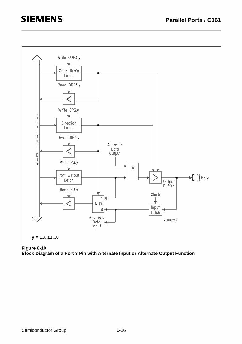
10Jul97@15:19h Parallel Ports / C161
Figure 6-10Block Diagram of a Port 3 Pin with Alternate Input or Alternate Output Function
y = 13, 11...0
Semiconductor Group 6-16
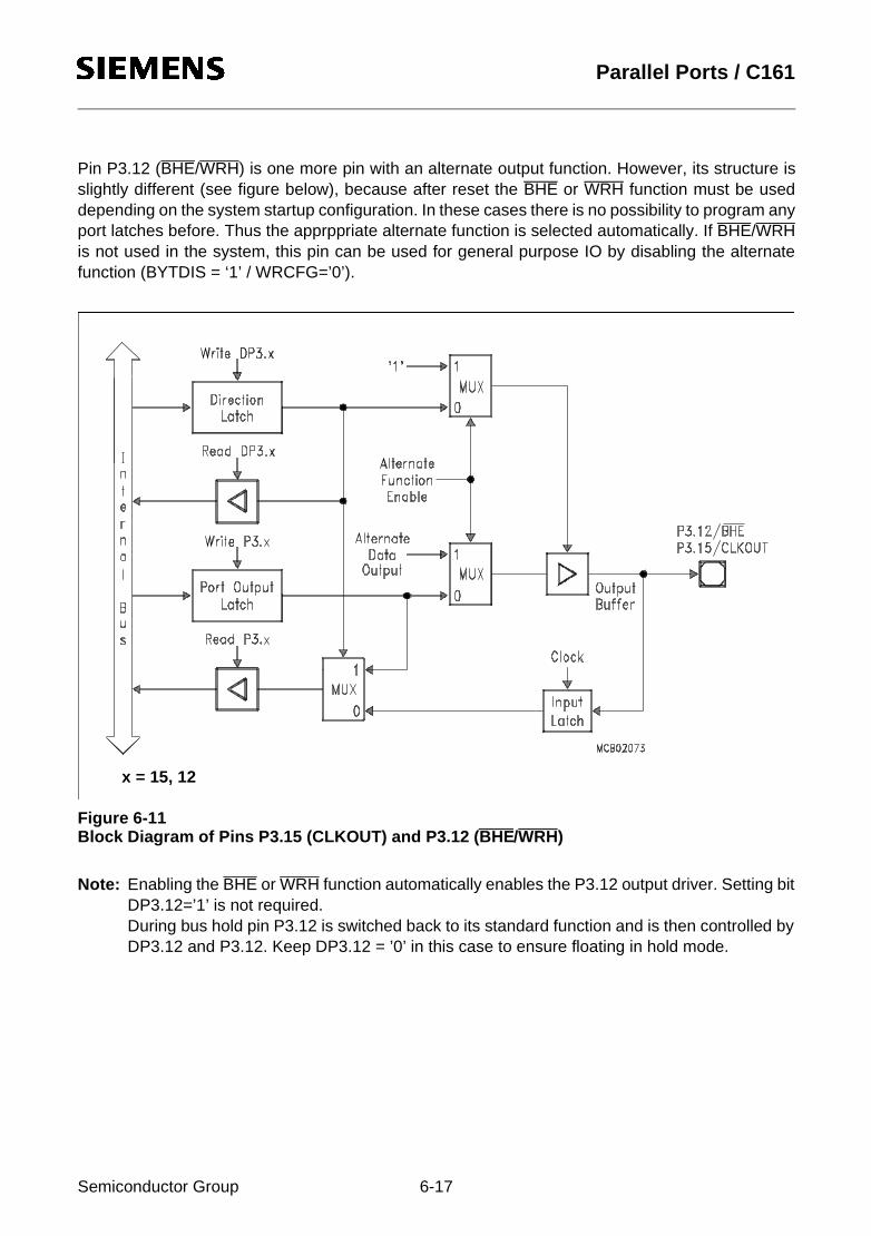
10Jul97@15:19h Parallel Ports / C161
Pin P3.12 (BHE/WRH) is one more pin with an alternate output function. However, its structure isslightly different (see figure below), because after reset the BHE or WRH function must be useddepending on the system startup configuration. In these cases there is no possibility to program anyport latches before. Thus the apprppriate alternate function is selected automatically. If BHE/WRHis not used in the system, this pin can be used for general purpose IO by disabling the alternatefunction (BYTDIS = ‘1’ / WRCFG=’0’).
Figure 6-11Block Diagram of Pins P3.15 (CLKOUT) and P3.12 (BHE/WRH)
Note: Enabling the BHE or WRH function automatically enables the P3.12 output driver. Setting bitDP3.12=’1’ is not required.During bus hold pin P3.12 is switched back to its standard function and is then controlled byDP3.12 and P3.12. Keep DP3.12 = ’0’ in this case to ensure floating in hold mode.
x = 15, 12
Semiconductor Group 6-17
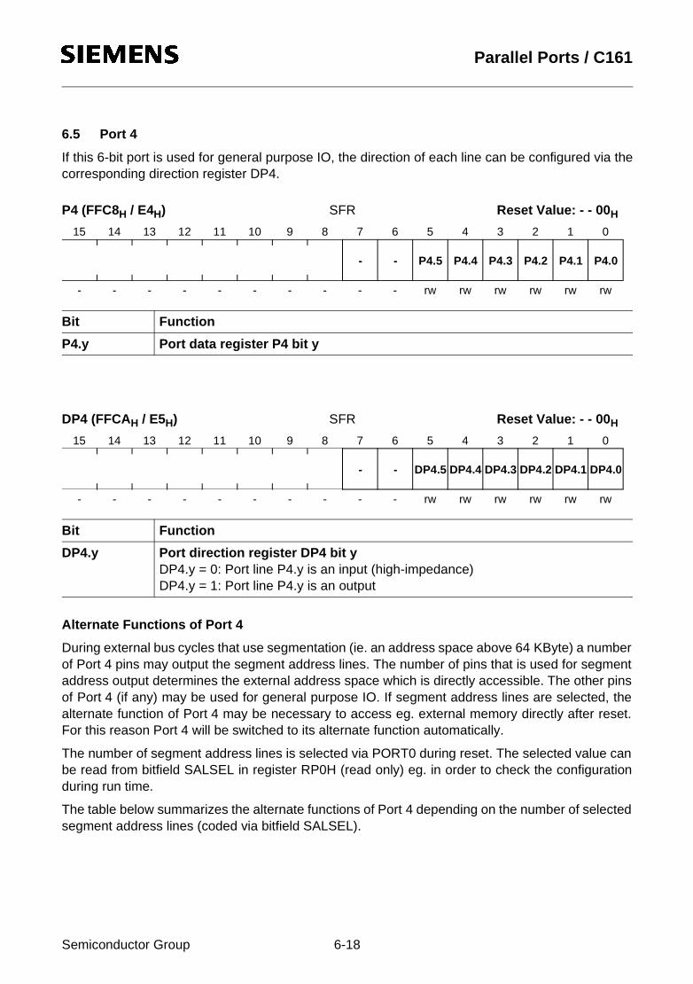
10Jul97@15:19h Parallel Ports / C161
6.5 Port 4
If this 6-bit port is used for general purpose IO, the direction of each line can be configured via thecorresponding direction register DP4.
P4 (FFC8H / E4H) SFR Reset Value: - - 00H
DP4 (FFCAH / E5H) SFR Reset Value: - - 00H
Alternate Functions of Port 4
During external bus cycles that use segmentation (ie. an address space above 64 KByte) a numberof Port 4 pins may output the segment address lines. The number of pins that is used for segmentaddress output determines the external address space which is directly accessible. The other pinsof Port 4 (if any) may be used for general purpose IO. If segment address lines are selected, thealternate function of Port 4 may be necessary to access eg. external memory directly after reset.For this reason Port 4 will be switched to its alternate function automatically.
The number of segment address lines is selected via PORT0 during reset. The selected value canbe read from bitfield SALSEL in register RP0H (read only) eg. in order to check the configurationduring run time.
The table below summarizes the alternate functions of Port 4 depending on the number of selectedsegment address lines (coded via bitfield SALSEL).
Bit Function
P4.y Port data register P4 bit y
Bit Function
DP4.y Port direction register DP4 bit yDP4.y = 0: Port line P4.y is an input (high-impedance)DP4.y = 1: Port line P4.y is an output
5 4 3 2 1 011 10 9 8 7 615 14 13 12
rw rw rw rw rw rw- - - - - -- - - -
P4.0P4.1P4.2P4.3P4.4P4.5--
5 4 3 2 1 011 10 9 8 7 615 14 13 12
rw rw rw rw rw rw- - - - - -- - - -
DP4.0DP4.1DP4.2DP4.3DP4.4DP4.5--
Semiconductor Group 6-18

10Jul97@15:19h Parallel Ports / C161
Figure 6-12Port 4 IO and Alternate Functions
Port 4 Pin Std. FunctionSALSEL=01 64 KB
Altern. FunctionSALSEL=11 256KB
Altern. FunctionSALSEL=00 1 MB
Altern. FunctionSALSEL=10 4 MB
P4.0P4.1P4.2P4.3P4.4P4.5
Gen. purpose IOGen. purpose IOGen. purpose IOGen. purpose IOGen. purpose IOGen. purpose IO
Seg. Address A16Seg. Address A17Gen. purpose IOGen. purpose IOGen. purpose IOGen. purpose IO
Seg. Address A16Seg. Address A17Seg. Address A18Seg. Address A19Gen. purpose IOGen. purpose IO
Seg. Address A16Seg. Address A17Seg. Address A18Seg. Address A19Seg. Address A20Seg. Address A21
----------P4.5P4.4P4.3P4.2P4.1P4.0
Port 4
----------A21A20A19A18A17A16
Alternate Function a)
General PurposeInput/Output
Semiconductor Group 6-19
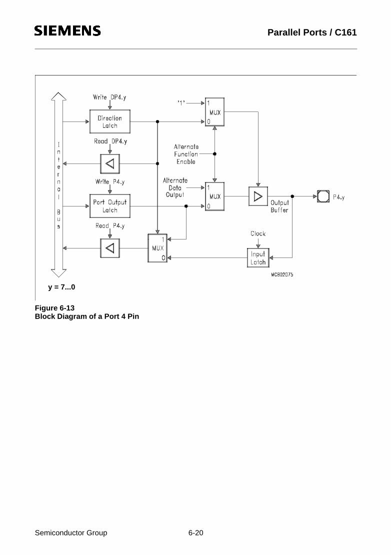
10Jul97@15:19h Parallel Ports / C161
Figure 6-13Block Diagram of a Port 4 Pin
y = 7...0
Semiconductor Group 6-20

10Jul97@15:19h Parallel Ports / C161
6.6 Port 5
This 2-bit input port can only read data. There is no output latch and no direction register. Datawritten to P5 will be lost.
P5 (FFA2H / D1H) SFR Reset Value: X - - -H
Alternate Functions of Port 5
Each line of Port 5 serves as external timer control line for GPT1.
The table below summarizes the alternate functions of Port 5.
Figure 6-14Port 5 IO and Alternate Functions
Note: The alternate functions of P5.15...P5.14 are only available on the C161K and the C161O.
Bit Function
P5.y Port data register P5 bit y (Read only)
Port 5 Pin Alternate Function
P5.14P5.15
T4EUD Timer 4 external Up/Down Control InputT2EUD Timer 2 external Up/Down Control Input
5 4 3 2 1 011 10 9 8 7 615 14 13 12
- - - - - -- - - - - -r r - -
P5.14P5.15
P5.15P5.14--------------
Port 5
T2EUDT4EUD--------------
Alternate Function a)
General PurposeInput
Semiconductor Group 6-21

10Jul97@15:19h Parallel Ports / C161
Port 5 pins have a special port structure (see figure below), because it is an input only port.
Figure 6-15Block Diagram of a Port 5 Pin
y = 15...10
Semiconductor Group 6-22
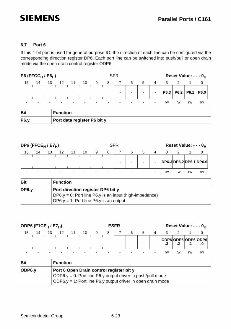
10Jul97@15:19h Parallel Ports / C161
6.7 Port 6
If this 4-bit port is used for general purpose IO, the direction of each line can be configured via thecorresponding direction register DP6. Each port line can be switched into push/pull or open drainmode via the open drain control register ODP6.
P6 (FFCCH / E6H) SFR Reset Value: - - - 0H
DP6 (FFCEH / E7H) SFR Reset Value: - - - 0H
ODP6 (F1CEH / E7H) ESFR Reset Value: - - - 0H
Bit Function
P6.y Port data register P6 bit y
Bit Function
DP6.y Port direction register DP6 bit yDP6.y = 0: Port line P6.y is an input (high-impedance)DP6.y = 1: Port line P6.y is an output
Bit Function
ODP6.y Port 6 Open Drain control register bit yODP6.y = 0: Port line P6.y output driver in push/pull modeODP6.y = 1: Port line P6.y output driver in open drain mode
5 4 3 2 1 011 10 9 8 7 615 14 13 12
- - rw rw rw rw- - - - - -- - - -
P6.0P6.1P6.2P6.3----
5 4 3 2 1 011 10 9 8 7 615 14 13 12
- - rw rw rw rw- - - - - -- - - -
DP6.0DP6.1DP6.2DP6.3----
ODP6.2
ODP6.1
ODP6.0
ODP6.3----
5 4 3 2 1 011 10 9 8 7 615 14 13 12
- - rw rw rw rw- - - - - -- - - -
Semiconductor Group 6-23
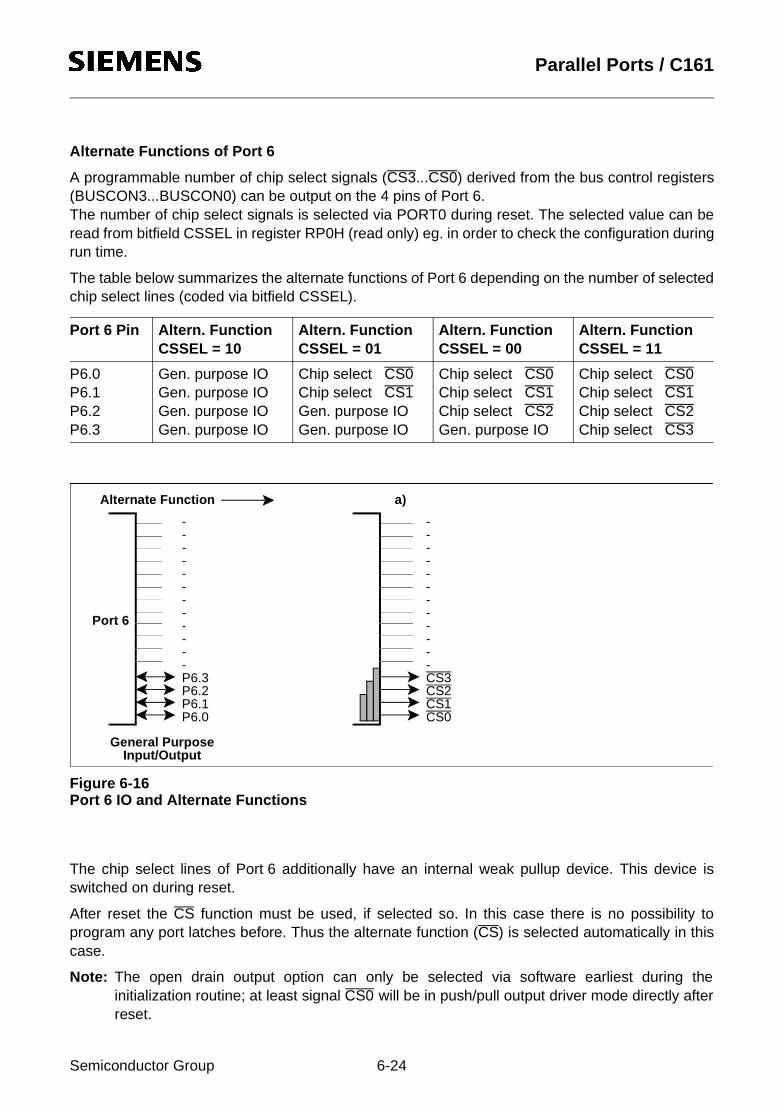
10Jul97@15:19h Parallel Ports / C161
Alternate Functions of Port 6
A programmable number of chip select signals (CS3...CS0) derived from the bus control registers(BUSCON3...BUSCON0) can be output on the 4 pins of Port 6.The number of chip select signals is selected via PORT0 during reset. The selected value can beread from bitfield CSSEL in register RP0H (read only) eg. in order to check the configuration duringrun time.
The table below summarizes the alternate functions of Port 6 depending on the number of selectedchip select lines (coded via bitfield CSSEL).
Figure 6-16Port 6 IO and Alternate Functions
The chip select lines of Port 6 additionally have an internal weak pullup device. This device isswitched on during reset.
After reset the CS function must be used, if selected so. In this case there is no possibility toprogram any port latches before. Thus the alternate function (CS) is selected automatically in thiscase.
Note: The open drain output option can only be selected via software earliest during theinitialization routine; at least signal CS0 will be in push/pull output driver mode directly afterreset.
Port 6 Pin Altern. FunctionCSSEL = 10
Altern. FunctionCSSEL = 01
Altern. FunctionCSSEL = 00
Altern. FunctionCSSEL = 11
P6.0P6.1P6.2P6.3
Gen. purpose IOGen. purpose IOGen. purpose IOGen. purpose IO
Chip select CS0Chip select CS1Gen. purpose IOGen. purpose IO
Chip select CS0Chip select CS1Chip select CS2Gen. purpose IO
Chip select CS0Chip select CS1Chip select CS2Chip select CS3
------------P6.3P6.2P6.1P6.0
Port 6
------------CS3CS2CS1CS0
Alternate Function a)
General PurposeInput/Output
Semiconductor Group 6-24

10Jul97@15:19h Parallel Ports / C161
Figure 6-17Block Diagram of Port 6 Pins with an alternate output function
Semiconductor Group 6-25
10Jul97@15:19h Dedicated Pins / C161
7 Dedicated Pins
Most of the input/output or control signals of the functional the C161 are realized as alternatefunctions of pins of the parallel ports. There is, however, a number of signals that use separate pins,including the oscillator, special control signals and, of course, the power supply.
The table below summarizes the 17 dedicated pins of the C161.
The Address Latch Enable signal ALE controls external address latches that provide a stableaddress in multiplexed bus modes.ALE is activated for every external bus cycle independent of the selected bus mode, ie. it is alsoactivated for bus cycles with a demultiplexed address bus. When an external bus is enabled (oneor more of the BUSACT bits set) also X-Peripheral accesses will generate an active ALE signal.ALE is not activated for internal accesses, ie. accesses to ROM/Flash (if provided), the internalRAM and the special function registers. In single chip mode, ie. when no external bus is enabled (noBUSACT bit set), ALE will also remain inactive for X-Peripheral accesses.
The External Read Strobe RD controls the output drivers of external memory or peripherals whenthe C161 reads data from these external devices. During reset and during Hold mode an internalpullup ensures an inactive (high) level on the RD output. During accesses to on-chip X-PeripheralsRD remains inactive (high).
The External Write Strobe WR/WRL controls the data transfer from the C161 to an externalmemory or peripheral device. This pin may either provide an general WR signal activated for bothbyte and word write accesses, or specifically control the low byte of an external 16-bit device (WRL)together with the signal WRH (alternate function of P3.12/BHE). During reset and during Hold modean internal pullup ensures an inactive (high) level on the WR/WRL output. During accesses to on-chip X-Peripherals WR/WRL remains inactive (high).
Pin(s) Function
ALE Address Latch Enable
RD External Read Strobe
WR/WRL External Write/Write Low Strobe
EA External Access Enable
NMI Non-Maskable Interrupt Input
RSTIN Reset Input
RSTOUT Reset Output
XTAL1, XTAL2 Oscillator Input/Output
VCC, VSS Digital Power Supply and Ground (4 pins each)
Semiconductor Group 7-1
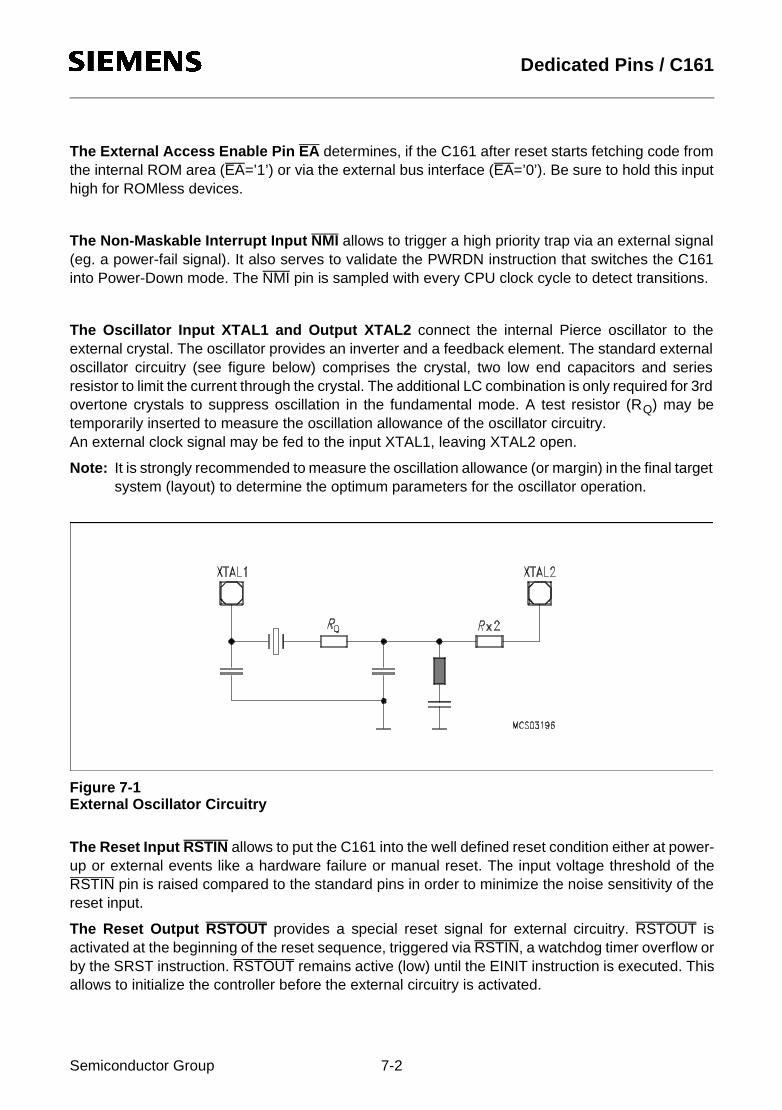
10Jul97@15:19h Dedicated Pins / C161
The External Access Enable Pin EA determines, if the C161 after reset starts fetching code fromthe internal ROM area (EA=’1’) or via the external bus interface (EA=’0’). Be sure to hold this inputhigh for ROMless devices.
The Non-Maskable Interrupt Input NMI allows to trigger a high priority trap via an external signal(eg. a power-fail signal). It also serves to validate the PWRDN instruction that switches the C161into Power-Down mode. The NMI pin is sampled with every CPU clock cycle to detect transitions.
The Oscillator Input XTAL1 and Output XTAL2 connect the internal Pierce oscillator to theexternal crystal. The oscillator provides an inverter and a feedback element. The standard externaloscillator circuitry (see figure below) comprises the crystal, two low end capacitors and seriesresistor to limit the current through the crystal. The additional LC combination is only required for 3rdovertone crystals to suppress oscillation in the fundamental mode. A test resistor (RQ) may betemporarily inserted to measure the oscillation allowance of the oscillator circuitry.An external clock signal may be fed to the input XTAL1, leaving XTAL2 open.
Note: It is strongly recommended to measure the oscillation allowance (or margin) in the final targetsystem (layout) to determine the optimum parameters for the oscillator operation.
Figure 7-1External Oscillator Circuitry
The Reset Input RSTIN allows to put the C161 into the well defined reset condition either at power-up or external events like a hardware failure or manual reset. The input voltage threshold of theRSTIN pin is raised compared to the standard pins in order to minimize the noise sensitivity of thereset input.
The Reset Output RSTOUT provides a special reset signal for external circuitry. RSTOUT isactivated at the beginning of the reset sequence, triggered via RSTIN, a watchdog timer overflow orby the SRST instruction. RSTOUT remains active (low) until the EINIT instruction is executed. Thisallows to initialize the controller before the external circuitry is activated.
Semiconductor Group 7-2

10Jul97@15:19h Dedicated Pins / C161
The Power Supply pins VCC and VSS provide the power supply for the digital logic of the C161.The respective VCC/VSS pairs should be decoupled as close to the pins as possible. For bestresults it is recommended to implement two-level decoupling, eg. (the widely used) 100 nF inparallel with 30...40 pF capacitors which deliver the peak currents.
Note: All VCC pins and all VSS pins must be connected to the power supply and ground,respectively.
Semiconductor Group 7-3
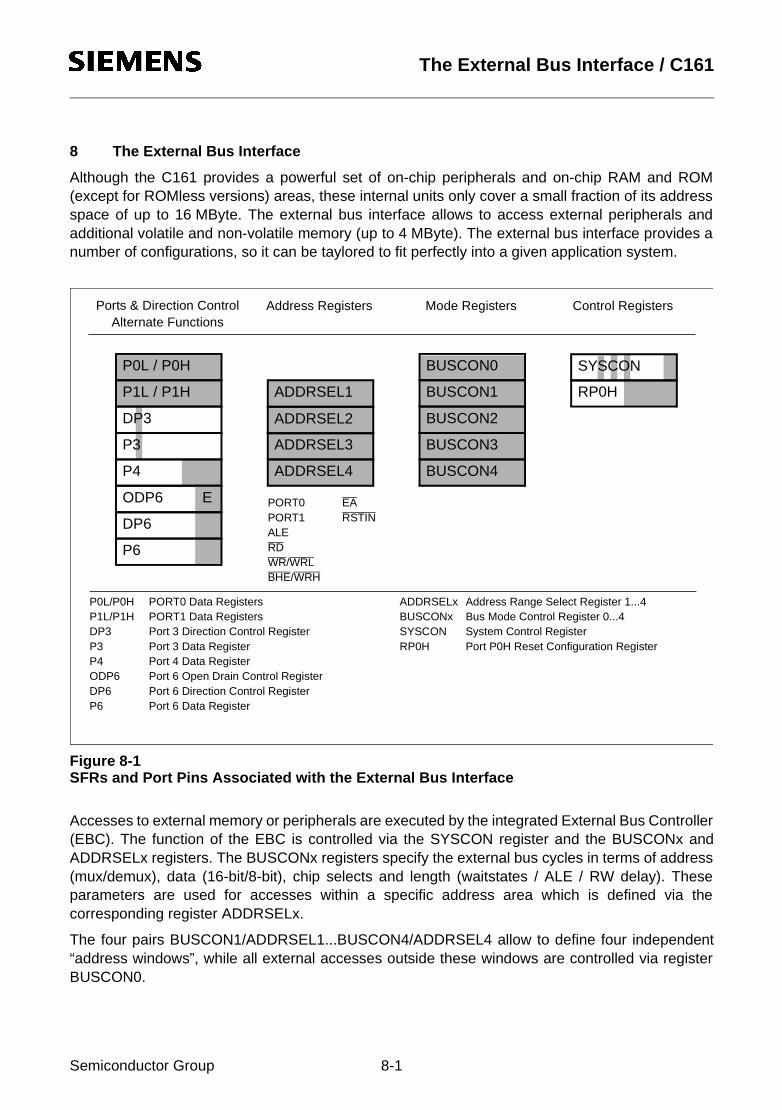
10Jul97@15:19h The External Bus Interface / C161
8 The External Bus Interface
Although the C161 provides a powerful set of on-chip peripherals and on-chip RAM and ROM(except for ROMless versions) areas, these internal units only cover a small fraction of its addressspace of up to 16 MByte. The external bus interface allows to access external peripherals andadditional volatile and non-volatile memory (up to 4 MByte). The external bus interface provides anumber of configurations, so it can be taylored to fit perfectly into a given application system.
Figure 8-1SFRs and Port Pins Associated with the External Bus Interface
Accesses to external memory or peripherals are executed by the integrated External Bus Controller(EBC). The function of the EBC is controlled via the SYSCON register and the BUSCONx andADDRSELx registers. The BUSCONx registers specify the external bus cycles in terms of address(mux/demux), data (16-bit/8-bit), chip selects and length (waitstates / ALE / RW delay). Theseparameters are used for accesses within a specific address area which is defined via thecorresponding register ADDRSELx.
The four pairs BUSCON1/ADDRSEL1...BUSCON4/ADDRSEL4 allow to define four independent“address windows”, while all external accesses outside these windows are controlled via registerBUSCON0.
BUSCON0
BUSCON1
BUSCON2
ADDRSEL4
P0L / P0H
P4
P6
ADDRSEL1
ODP6 E
P0L/P0H PORT0 Data RegistersP1L/P1H PORT1 Data RegistersDP3 Port 3 Direction Control RegisterP3 Port 3 Data RegisterP4 Port 4 Data RegisterODP6 Port 6 Open Drain Control RegisterDP6 Port 6 Direction Control RegisterP6 Port 6 Data Register
PORT0 EAPORT1 RSTINALERDWR/WRLBHE/WRH
SYSCON
Control Registers
ADDRSELx Address Range Select Register 1...4BUSCONx Bus Mode Control Register 0...4SYSCON System Control RegisterRP0H Port P0H Reset Configuration Register
Ports & Direction ControlAlternate Functions
Address Registers Mode Registers Control Registers
BUSCON3
P1L / P1H
BUSCON4
ADDRSEL2
RP0H
DP6
DP3
P3 ADDRSEL3
Semiconductor Group 8-1
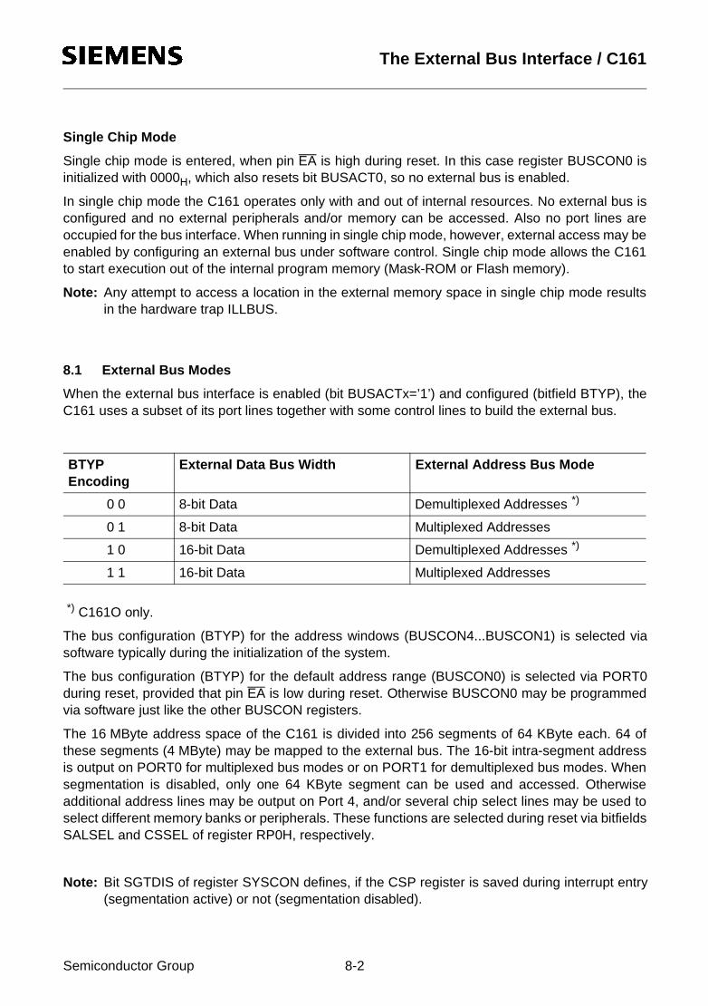
10Jul97@15:19h The External Bus Interface / C161
Single Chip Mode
Single chip mode is entered, when pin EA is high during reset. In this case register BUSCON0 isinitialized with 0000H, which also resets bit BUSACT0, so no external bus is enabled.
In single chip mode the C161 operates only with and out of internal resources. No external bus isconfigured and no external peripherals and/or memory can be accessed. Also no port lines areoccupied for the bus interface. When running in single chip mode, however, external access may beenabled by configuring an external bus under software control. Single chip mode allows the C161to start execution out of the internal program memory (Mask-ROM or Flash memory).
Note: Any attempt to access a location in the external memory space in single chip mode resultsin the hardware trap ILLBUS.
8.1 External Bus Modes
When the external bus interface is enabled (bit BUSACTx=’1’) and configured (bitfield BTYP), theC161 uses a subset of its port lines together with some control lines to build the external bus.
*) C161O only.
The bus configuration (BTYP) for the address windows (BUSCON4...BUSCON1) is selected viasoftware typically during the initialization of the system.
The bus configuration (BTYP) for the default address range (BUSCON0) is selected via PORT0during reset, provided that pin EA is low during reset. Otherwise BUSCON0 may be programmedvia software just like the other BUSCON registers.
The 16 MByte address space of the C161 is divided into 256 segments of 64 KByte each. 64 ofthese segments (4 MByte) may be mapped to the external bus. The 16-bit intra-segment addressis output on PORT0 for multiplexed bus modes or on PORT1 for demultiplexed bus modes. Whensegmentation is disabled, only one 64 KByte segment can be used and accessed. Otherwiseadditional address lines may be output on Port 4, and/or several chip select lines may be used toselect different memory banks or peripherals. These functions are selected during reset via bitfieldsSALSEL and CSSEL of register RP0H, respectively.
Note: Bit SGTDIS of register SYSCON defines, if the CSP register is saved during interrupt entry(segmentation active) or not (segmentation disabled).
BTYP Encoding
External Data Bus Width External Address Bus Mode
0 0 8-bit Data Demultiplexed Addresses *)
0 1 8-bit Data Multiplexed Addresses
1 0 16-bit Data Demultiplexed Addresses *)
1 1 16-bit Data Multiplexed Addresses
Semiconductor Group 8-2

10Jul97@15:19h The External Bus Interface / C161
Multiplexed Bus Modes
In the multiplexed bus modes the 16-bit intra-segment address as well as the data use PORT0. Theaddress is time-multiplexed with the data and has to be latched externally. The width of the requiredlatch depends on the selected data bus width, ie. an 8-bit data bus requires a byte latch (the addressbits A15...A8 on P0H do not change, while P0L multiplexes address and data), a 16-bit data busrequires a word latch (the least significant address line A0 is not relevant for word accesses).The upper address lines (An...A16) are permanently output on Port 4 (if segmentation is enabled)and do not require latches.
The EBC initiates an external access by generating the Address Latch Enable signal (ALE) andthen placing an address on the bus. The falling edge of ALE triggers an external latch to capture theaddress. After a period of time during which the address must have been latched externally, theaddress is removed from the bus. The EBC now activates the respective command signal (RD, WR,WRL, WRH). Data is driven onto the bus either by the EBC (for write cycles) or by the externalmemory/peripheral (for read cycles). After a period of time, which is determined by the access timeof the memory/peripheral, data become valid.
Read cycles: Input data is latched and the command signal is now deactivated. This causes theaccessed device to remove its data from the bus which is then tri-stated again.
Write cycles: The command signal is now deactivated. The data remain valid on the bus until thenext external bus cycle is started.
Figure 8-2Multiplexed Bus Cycle
Semiconductor Group 8-3

10Jul97@15:19h The External Bus Interface / C161
Demultiplexed Bus Modes
In the demultiplexed bus modes the 16-bit intra-segment address is permanently output on PORT1,while the data uses PORT0 (16-bit data) or P0L (8-bit data).The upper address lines are permanently output on Port 4 (if selected via SALSEL during reset). Noaddress latches are required.
The EBC initiates an external access by placing an address on the address bus. After aprogrammable period of time the EBC activates the respective command signal (RD, WR, WRL,WRH). Data is driven onto the data bus either by the EBC (for write cycles) or by the externalmemory/peripheral (for read cycles). After a period of time, which is determined by the access timeof the memory/peripheral, data become valid.
Read cycles: Input data is latched and the command signal is now deactivated. This causes theaccessed device to remove its data from the data bus which is then tri-stated again.
Write cycles: The command signal is now deactivated. If a subsequent external bus cycle isrequired, the EBC places the respective address on the address bus. The data remain valid on thebus until the next external bus cycle is started.
Figure 8-3Demultiplexed Bus Cycle
Note: Demultiplexed bus modes are only provided on the C161O.
Semiconductor Group 8-4

10Jul97@15:19h The External Bus Interface / C161
Switching between the Bus Modes
The EBC allows to switch between different bus modes dynamically, ie. subsequent external buscycles may be executed in different ways. Certain address areas may use multiplexed ordemultiplexed buses or use predefined waitstates.
A change of the external bus characteristics can be initiated in two different ways:
Reprogramming the BUSCON and/or ADDRSEL registers allows to either change the bus modefor a given address window, or change the size of an address window that uses a certain bus mode.Reprogramming allows to use a great number of different address windows (more than BUSCONsare available) on the expense of the overhead for changing the registers and keeping appropriatetables.
Switching between predefined address windows automatically selects the bus mode that isassociated with the respective window. Predefined address windows allow to use different busmodes without any overhead, but restrict their number to the number of BUSCONs. However, asBUSCON0 controls all address areas, which are not covered by the other BUSCONs, this allows tohave gaps between these windows, which use the bus mode of BUSCON0.
PORT1 will output the intra-segment address, when any of the BUSCON registers selects ademultiplexed bus mode, even if the current bus cycle uses a multiplexed bus mode. This allows tohave an external address decoder connected to PORT1 only, while using it for all kinds of buscycles.
Note: Never change the configuration for an address area that currently supplies the instructionstream. Due to the internal pipelining it is very difficult to determine the first instruction fetchthat will use the new configuration. Only change the configuration for address areas that arenot currently accessed. This applies to BUSCON registers as well as to ADDRSEL registers.
The usage of the BUSCON/ADDRSEL registers is controlled via the issued addresses. When anaccess (code fetch or data) is initiated, the respective generated physical address defines, if theaccess is made internally, uses one of the address windows defined by ADDRSEL4...1, or uses thedefault configuration in BUSCON0. After initializing the active registers, they are selected andevaluated automatically by interpreting the physical address. No additional switching or selecting isnecessary during run time, except when more than the four address windows plus the default is tobe used.
Switching from demultiplexed to multiplexed bus mode represents a special case. The buscycle is started by activating ALE and driving the address to Port 4 and PORT1 as usual, if anotherBUSCON register selects a demultiplexed bus. However, in the multiplexed bus modes the addressis also required on PORT0. In this special case the address on PORT0 is delayed by one CPU clockcycle, which delays the complete (multiplexed) bus cycle and extends the corresponding ALE signal(see figure below).
This extra time is required to allow the previously selected device (via demultiplexed bus) to releasethe data bus, which would be available in a demultiplexed bus cycle.
Semiconductor Group 8-5
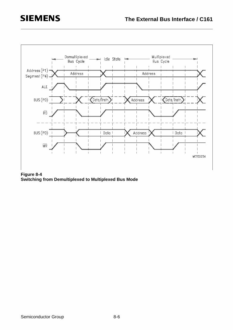
10Jul97@15:19h The External Bus Interface / C161
Figure 8-4Switching from Demultiplexed to Multiplexed Bus Mode
Semiconductor Group 8-6

10Jul97@15:19h The External Bus Interface / C161
External Data Bus Width
The EBC can operate on 8-bit or 16-bit wide external memory/peripherals. A 16-bit data bus usesPORT0, while an 8-bit data bus only uses P0L, the lower byte of PORT0. This saves on addresslatches, bus transceivers, bus routing and memory cost on the expense of transfer time. The EBCcan control word accesses on an 8-bit data bus as well as byte accesses on a 16-bit data bus.
Word accesses on an 8-bit data bus are automatically split into two subsequent byte accesses,where the low byte is accessed first, then the high byte. The assembly of bytes to words and thedisassembly of words into bytes is handled by the EBC and is transparent to the CPU and theprogrammer.
Byte accesses on a 16-bit data bus require that the upper and lower half of the memory can beaccessed individually. In this case the upper byte is selected with the BHE signal, while the lowerbyte is selected with the A0 signal. So the two bytes of the memory can be enabled independentfrom each other, or together when accessing words.
When writing bytes to an external 16-bit device, which has a single CS input, but two WR enableinputs (for the two bytes), the EBC can directly generate these two write control signals. This savesthe external combination of the WR signal with A0 or BHE. In this case pin WR serves as WRL (writelow byte) and pin BHE serves as WRH (write high byte). Bit WRCFG in register SYSCON selectsthe operating mode for pins WR and BHE. The respective byte will be written on both data bus halfs.
When reading bytes from an external 16-bit device, whole words may be read and the C161automatically selects the byte to be input and discards the other. However, care must be takenwhen reading devices that change state when being read, like FIFOs, interrupt status registers, etc.In this case individual bytes should be selected using BHE and A0.
Note: PORT1 gets available for general purpose IO, when none of the BUSCON registers selectsa demultiplexed bus mode (where available).
Disable/Enable Control for Pin BHE (BYTDIS) Bit BYTDIS is provided for controlling the active low Byte High Enable (BHE) pin. The function of theBHE pin is enabled, if the BYTDIS bit contains a ’0’. Otherwise, it is disabled and the pin can be usedas standard IO pin. The BHE pin is implicitly used by the External Bus Controller to select one of twobyte-organized memory chips, which are connected to the C161 via a word-wide external data bus.After reset the BHE function is automatically enabled (BYTDIS = ’0’), if a 16-bit data bus is selectedduring reset, otherwise it is disabled (BYTDIS=’1’). It may be disabled, if byte access to 16-bitmemory is not required, and the BHE signal is not used.
Bus Mode Transfer Rate (Speed factor for byte/word/dword access)
System Requirements Free IO Lines
8-bit Multiplexed Very low ( 1.5 / 3 / 6 ) Low (8-bit latch, byte bus) P1H, P1L
8-bit Demultipl. Low ( 1 / 2 / 4 ) Very low (no latch, byte bus) P0H
16-bit Multiplexed High ( 1.5 / 1.5 / 3 ) High (16-bit latch, word bus) P1H, P1L
16-bit Demultipl. Very high ( 1 / 1 / 2 ) Low (no latch, word bus) ---
Semiconductor Group 8-7
10Jul97@15:19h The External Bus Interface / C161
Segment Address Generation
During external accesses the EBC generates a (programmable) number of address lines on Port 4,which extend the 16-bit address output on PORT0 or PORT1, and so increase the accessibleaddress space. The number of segment address lines is selected during reset and coded in bit fieldSALSEL in register RP0H (see table below).
Note: The total accessible address space may be increased by accessing several banks which aredistinguished by individual chip select signals.
CS Signal Generation
During external accesses the EBC can generate a (programmable) number of CS lines on Port 6,which allow to directly select external peripherals or memory banks without requiring an externaldecoder. The number of CS lines is selected during reset and coded in bit field CSSEL in registerRP0H (see table below).
The CSx outputs are associated with the BUSCONx registers and are driven active (low) for anyaccess within the address area defined for the respective BUSCON register. For any accessoutside this defined address area the respective CSx signal will go inactive (high). At the beginningof each external bus cycle the corresponding valid CS signal is determined and activated. All otherCS lines are deactivated (driven high) at the same time.
Note: The CSx signals will not be updated for an access to any internal address area (ie. when noexternal bus cycle is started), even if this area is covered by the respective ADDRSELxregister. An access to an on-chip X-Peripheral deactivates all external CS signals.Upon accesses to address windows without a selected CS line all selected CS lines aredeactivated.The CSx signals are not available on the C161V.
SALSEL Segment Address Lines Directly accessible Address Space
1 1 Two: A17...A16 256 KByte (Default without pull-downs)
1 0 Six: A21...A16 4 MByte (Maximum)
0 1 None 64 KByte (Minimum)
0 0 Four: A19...A16 1 MByte
CSSEL Chip Select Lines Note
1 1 Four: CS3...CS0 Default without pull-downs
1 0 None Port 6 pins free for IO
0 1 Two: CS1...CS0
0 0 Three: CS2...CS0
Semiconductor Group 8-8

10Jul97@15:19h The External Bus Interface / C161
The chip select signals allow to be operated in four different modes, which are selected via bitsCSWENx and CSRENx in the respective BUSCONx register.
Address Chip Select signals remain active until an access to another address window. An addresschip select becomes active with the falling edge of ALE and becomes inactive with the falling edgeof ALE of an external bus cycle that accesses a different address area. No spikes will be generatedon the chip select lines.
Read or Write Chip Select signals remain active only as long as the associated control signal (RDor WR) is active. This also includes the programmable read/write delay. Read chip select is onlyactivated for read cycles, write chip select is only activated for write cycles, read/write chip select isactivated for both read and write cycles (write cycles are assumed, if any of the signals WRH orWRL gets active). These modes save external glue logic, when accessing external devices likelatches or drivers that only provide a single enable input.
Note: CS0 provides an address chip select directly after reset (except for single chip mode) whenthe first instruction is fetched.
Internal pullup devices hold all CS lines high during reset. After the end of a reset sequence thepullup devices are switched off and the pin drivers control the pin levels on the selected CS lines.Not selected CS lines will enter the high-impedance state and are available for general purpose IO.
Segment Address versus Chip Select
The external bus interface of the C161 supports many configurations for the external memory. Byincreasing the number of segment address lines the C161 can address a linear address space of256 KByte, 1 MByte or 4 MByte. This allows to implement a large sequential memory area, and alsoallows to access a great number of external devices, using an external decoder. By increasing thenumber of CS lines the C161 can access memory banks or peripherals without external glue logic.These two features may be combined to optimize the overall system performance. Enabling 4segment address lines and 5 chip select lines eg. allows to access five memory banks of 1 MByteeach. So the available address space is 5 MByte (without glue logic).
Note: Bit SGTDIS of register SYSCON defines, if the CSP register is saved during interrupt entry(segmentation active) or not (segmentation disabled).
CSWENx CSRENx Chip Select Mode
0 0 Address Chip Select (Default after Reset, mode for CS0)
0 1 Read Chip Select
1 0 Write Chip Select
1 1 Read/Write Chip Select
Semiconductor Group 8-9

10Jul97@15:19h The External Bus Interface / C161
8.2 Programmable Bus Characteristics
Important timing characteristics of the external bus interface have been made user programmableto allow to adapt it to a wide range of different external bus and memory configurations with differenttypes of memories and/or peripherals.
The following parameters of an external bus cycle are programmable:
• ALE Control defines the ALE signal length and the address hold time after its falling edge• Memory Cycle Time (extendable with 1...15 waitstates) defines the allowable access time• Memory Tri-State Time (extendable with 1 waitstate) defines the time for a data driver to float• Read/Write Delay Time defines when a command is activated after the falling edge of ALE
Note: Internal accesses are executed with maximum speed and therefore are not programmable.External acceses use the slowest possible bus cycle after reset. The bus cycle timing maythen be optimized by the initialization software.
Figure 8-5Programmable External Bus Cycle
ALECTL MCTC MTTC
Semiconductor Group 8-10

10Jul97@15:19h The External Bus Interface / C161
ALE Length Control
The length of the ALE signal and the address hold time after its falling edge are controlled by theALECTLx bits in the BUSCON registers. When bit ALECTL is set to ‘1’, external bus cyclesaccessing the respective address window will have their ALE signal prolonged by half a CPU clock(31.25 ns at fCPU = 16 MHz). Also the address hold time after the falling edge of ALE (on amultiplexed bus) will be prolonged by half a CPU clock, so the data transfer within a bus cycle refersto the same CLKOUT edges as usual (ie. the data transfer is delayed by one CPU clock). Thisallows more time for the address to be latched.
Note: ALECTL0 is ‘1’ after reset to select the slowest possible bus cycle, the other ALECTLx are‘0’ after reset.
Figure 8-6ALE Length Control
Semiconductor Group 8-11
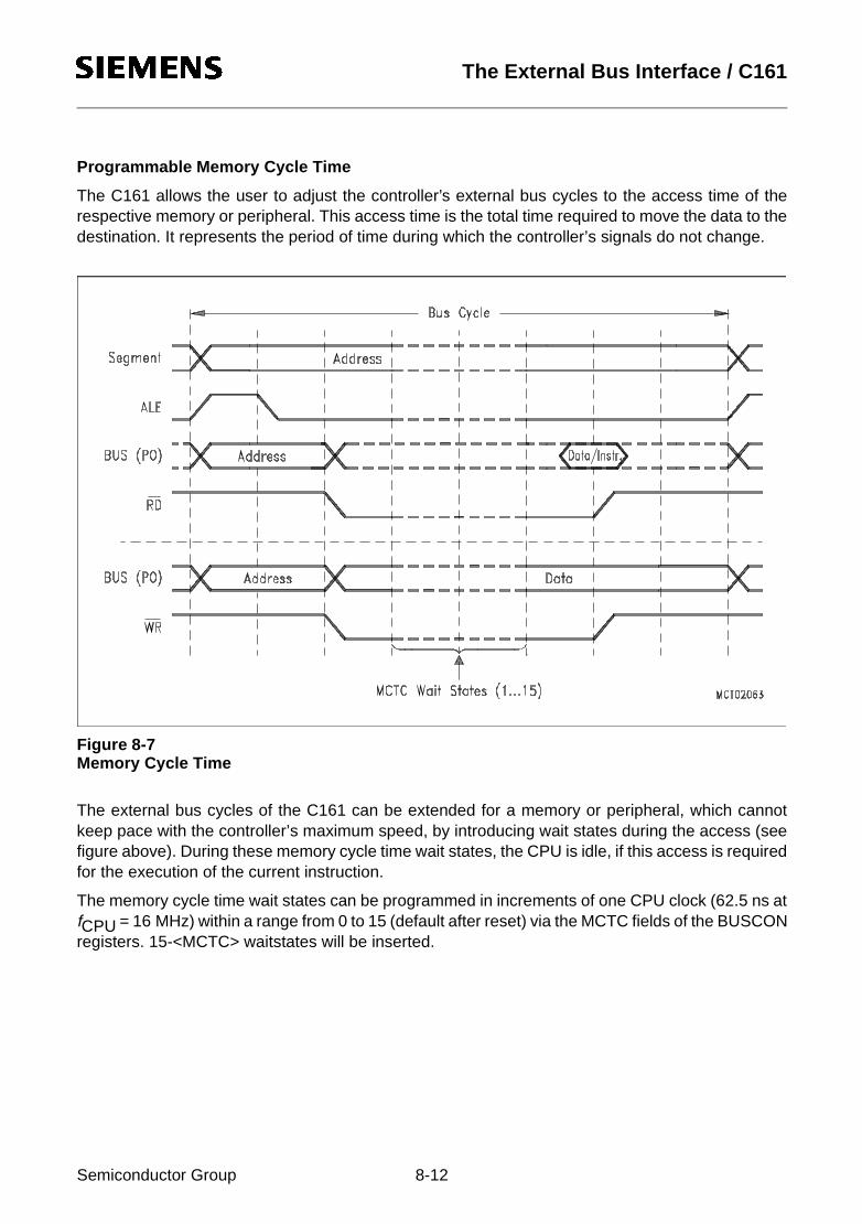
10Jul97@15:19h The External Bus Interface / C161
Programmable Memory Cycle Time
The C161 allows the user to adjust the controller’s external bus cycles to the access time of therespective memory or peripheral. This access time is the total time required to move the data to thedestination. It represents the period of time during which the controller’s signals do not change.
Figure 8-7Memory Cycle Time
The external bus cycles of the C161 can be extended for a memory or peripheral, which cannotkeep pace with the controller’s maximum speed, by introducing wait states during the access (seefigure above). During these memory cycle time wait states, the CPU is idle, if this access is requiredfor the execution of the current instruction.
The memory cycle time wait states can be programmed in increments of one CPU clock (62.5 ns atfCPU = 16 MHz) within a range from 0 to 15 (default after reset) via the MCTC fields of the BUSCONregisters. 15-<MCTC> waitstates will be inserted.
Semiconductor Group 8-12

10Jul97@15:19h The External Bus Interface / C161
Programmable Memory Tri-State Time
The C161 allows the user to adjust the time between two subsequent external accesses to accountfor the tri-state time of the external device. The tri-state time defines, when the external device hasreleased the bus after deactivation of the read command (RD).
Figure 8-8Memory Tri-State Time
The output of the next address on the external bus can be delayed for a memory or peripheral,which needs more time to switch off its bus drivers, by introducing a wait state after the previous buscycle (see figure above). During this memory tri-state time wait state, the CPU is not idle, so CPUoperations will only be slowed down if a subsequent external instruction or data fetch operation isrequired during the next instruction cycle.
The memory tri-state time waitstate requires one CPU clock (62.5 ns at fCPU = 16 MHz) and iscontrolled via the MTTCx bits of the BUSCON registers. A waitstate will be inserted, if bit MTTCx is‘0’ (default after reset).
Note: External bus cycles in multiplexed bus modes implicitly add one tri-state time waitstate inaddition to the programmable MTTC waitstate.
Semiconductor Group 8-13

10Jul97@15:19h The External Bus Interface / C161
Read/Write Signal Delay
The C161 allows the user to adjust the timing of the read and write commands to account for timingrequirements of external peripherals. The read/write delay controls the time between the fallingedge of ALE and the falling edge of the command. Without read/write delay the falling edges of ALEand command(s) are coincident (except for propagation delays). With the delay enabled, thecommand(s) become active half a CPU clock (31.25 ns at fCPU = 16 MHz) after the falling edge ofALE.The read/write delay does not extend the memory cycle time, and does not slow down the controllerin general. In multiplexed bus modes, however, the data drivers of an external device may conflictwith the C161’s address, when the early RD signal is used. Therefore multiplexed bus cycles shouldalways be programmed with read/write delay.
Figure 8-9Read/Write Delay
The read/write delay is controlled via the RWDCx bits in the BUSCON registers. The command(s)will be delayed, if bit RWDCx is ‘0’ (default after reset).
1) The data drivers from the previous bus cycle should be disabled when the RD signal becomes active.
Semiconductor Group 8-14
10Jul97@15:19h The External Bus Interface / C161
8.3 Controlling the External Bus Controller
A set of registers controls the functions of the EBC. General features like the usage of interface pins(WR, BHE), segmentation and internal ROM mapping are controlled via register SYSCON. Theproperties of a bus cycle like chip select mode, length of ALE, external bus mode, read/write delayand waitstates are controlled via registers BUSCON4...BUSCON0. Four of these registers(BUSCON4...BUSCON1) have an address select register (ADDRSEL4...ADDRSEL1) associatedwith them, which allows to specify up to four address areas and the individual bus characteristicswithin these areas. All accesses that are not covered by these four areas are then controlled viaBUSCON0. This allows to use memory components or peripherals with different interfaces withinthe same system, while optimizing accesses to each of them.
Semiconductor Group 8-15

10Jul97@15:19h The External Bus Interface / C161
SYSCON (FF12H / 89H) SFR Reset Value: 0XX0H
Note: Register SYSCON cannot be changed after execution of the EINIT instruction.Bit SGTDIS controls the correct stack operation (push/pop of CSP or not) during traps andinterrupts.
Bit Function
XPER-SHARE XBUS Peripheral Share Mode Control‘0’: External accesses to XBUS peripherals are disabled‘1’: XBUS peripherals are accessible via the external bus during hold mode
VISIBLE Visible Mode Control‘0’: Accesses to XBUS peripherals are done internally‘1’: XBUS peripheral accesses are made visible on the external pins
XPEN XBUS Peripheral Enable Bit‘0’: Accesses to the on-chip X-Peripherals and their functions are disabled‘1’: The on-chip X-Peripherals are enabled and can be accessed
WRCFG Write Configuration Control (Set according to pin P0H.0 during reset)‘0’: Pins WR and BHE retain their normal function‘1’: Pin WR acts as WRL, pin BHE acts as WRH
BYTDIS Disable/Enable Control for Pin BHE (Set according to data bus width)‘0’: Pin BHE enabled‘1’: Pin BHE disabled, pin may be used for general purpose IO
ROMEN Internal ROM Enable (Set according to pin EA during reset)‘0’: Internal ROM disabled: accesses to the ROM area use the external bus‘1’: Internal ROM enabled
SGTDIS Segmentation Disable/Enable Control‘0’: Segmentation enabled (CSP is saved/restored during interrupt entry/exit)‘1’: Segmentation disabled (Only IP is saved/restored)
ROMS1 Internal ROM Mapping‘0’: Internal ROM area mapped to segment 0 (00’0000H...00’7FFFH)‘1’: Internal ROM area mapped to segment 1 (01’0000H...01’7FFFH)
STKSZ System Stack SizeSelects the size of the system stack (in the internal RAM) from 32 to 1024 words
-- XPENXPER-SHARE
VISIBLE- - -
ROMS1
WRCFG
5 4 3 2 1 011 10 9 8 7 615 14 13 12
- - rwrw rw rwrw rw
STKSZSGTDIS
ROMEN
rw
BYTDIS
- - rw rw-
Semiconductor Group 8-16

10Jul97@15:19h The External Bus Interface / C161
The layout of the five BUSCON registers is identical. Registers BUSCON4...BUSCON1, whichcontrol the selected address windows, are completely under software control, while registerBUSCON0, which eg. is also used for the very first code access after reset, is partly controlled byhardware, ie. it is initialized via PORT0 during the reset sequence. This hardware control allows todefine an appropriate external bus for systems, where no internal program memory is provided.
BUSCON0 (FF0CH / 86H) SFR Reset Value: 0XX0H
BUSCON1 (FF14H / 8AH) SFR Reset Value: 0000H
BUSCON2 (FF16H / 8BH) SFR Reset Value: 0000H
BUSCON3 (FF18H / 8CH) SFR Reset Value: 0000H
BUSCON4 (FF1AH / 8DH) SFR Reset Value: 0000H
Note: BUSCON0 is initialized with 0000H, if pin EA is high during reset. If pin EA is low during reset,bits BUSACT0 and ALECTL0 are set (‘1’) and bit field BTYP is loaded with the busconfiguration selected via PORT0.
---CSWEN0
CSREN0 -
MTTC0
RWDC0
5 4 3 2 1 011 10 9 8 7 615 14 13 12
rw rw- rw rwrw rwrw - -
BUSACT0
rw
ALECTL0
- rw
BTYP MCTC
-- --MTTC1
RWDC1
5 4 3 2 1 011 10 9 8 7 615 14 13 12
rw rw- rw rwrw rw
BTYP MCTC
rw - -
BUSACT1
rw
ALECTL1
- rw
CSWEN1
CSREN1
-- --MTTC2
RWDC2
5 4 3 2 1 011 10 9 8 7 615 14 13 12
rw rw- rw rwrw rw
BTYP MCTC
rw - -
BUSACT2
rw
ALECTL2
- rw
CSWEN2
CSREN2
-- --MTTC3
RWDC3
5 4 3 2 1 011 10 9 8 7 615 14 13 12
rw rw- rw rwrw rw
BTYP MCTC
rw - -
BUSACT3
rw
ALECTL3
- rw
CSWEN3
CSREN3
-- --MTTC4
RWDC4
5 4 3 2 1 011 10 9 8 7 615 14 13 12
rw rw- rw rwrw rw
BTYP MCTC
rw - -
BUSACT4
rw
ALECTL4
- rw
CSWEN4
CSREN4
Semiconductor Group 8-17
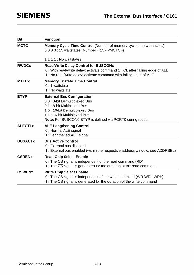
10Jul97@15:19h The External Bus Interface / C161
Bit Function
MCTC Memory Cycle Time Control (Number of memory cycle time wait states)0 0 0 0 : 15 waitstates (Number = 15 - <MCTC>). . .1 1 1 1 : No waitstates
RWDCx Read/Write Delay Control for BUSCONx‘0’: With read/write delay: activate command 1 TCL after falling edge of ALE‘1’: No read/write delay: activate command with falling edge of ALE
MTTCx Memory Tristate Time Control‘0’: 1 waitstate‘1’: No waitstate
BTYP External Bus Configuration0 0 : 8-bit Demultiplexed Bus0 1 : 8-bit Multiplexed Bus1 0 : 16-bit Demultiplexed Bus1 1 : 16-bit Multiplexed BusNote: For BUSCON0 BTYP is defined via PORT0 during reset.
ALECTLx ALE Lengthening Control‘0’: Normal ALE signal‘1’: Lengthened ALE signal
BUSACTx Bus Active Control‘0’: External bus disabled‘1’: External bus enabled (within the respective address window, see ADDRSEL)
CSRENx Read Chip Select Enable‘0’: The CS signal is independent of the read command (RD)‘1’: The CS signal is generated for the duration of the read command
CSWENx Write Chip Select Enable‘0’: The CS signal is independent of the write command (WR,WRL,WRH)‘1’: The CS signal is generated for the duration of the write command
Semiconductor Group 8-18

10Jul97@15:19h The External Bus Interface / C161
ADDRSEL1 (FE18H / 0CH) SFR Reset Value: 0000H
ADDRSEL2 (FE1AH / 0DH) SFR Reset Value: 0000H
ADDRSEL3(FE1CH / 0EH) SFR Reset Value: 0000H
ADDRSEL4 (FE1EH / 0FH) SFR Reset Value: 0000H
Note: There is no register ADDRSEL0, as register BUSCON0 controls all external accessesoutside the four address windows of BUSCON4...BUSCON1 within the complete addressspace.
Bit Function
RGSZ Range Size SelectionDefines the size of the address area controlled by the respective BUSCONx/ADDRSELx register pair. See table below.
RGSAD Range Start AddressDefines the upper bits of the start address (A23...) of the respective address area. See table below.
5 4 3 2 1 011 10 9 8 7 615 14 13 12
rw
RGSAD RGSZ
rw
5 4 3 2 1 011 10 9 8 7 615 14 13 12
rw
RGSAD RGSZ
rw
5 4 3 2 1 011 10 9 8 7 615 14 13 12
rw
RGSAD RGSZ
rw
5 4 3 2 1 011 10 9 8 7 615 14 13 12
rw
RGSAD RGSZ
rw
Semiconductor Group 8-19
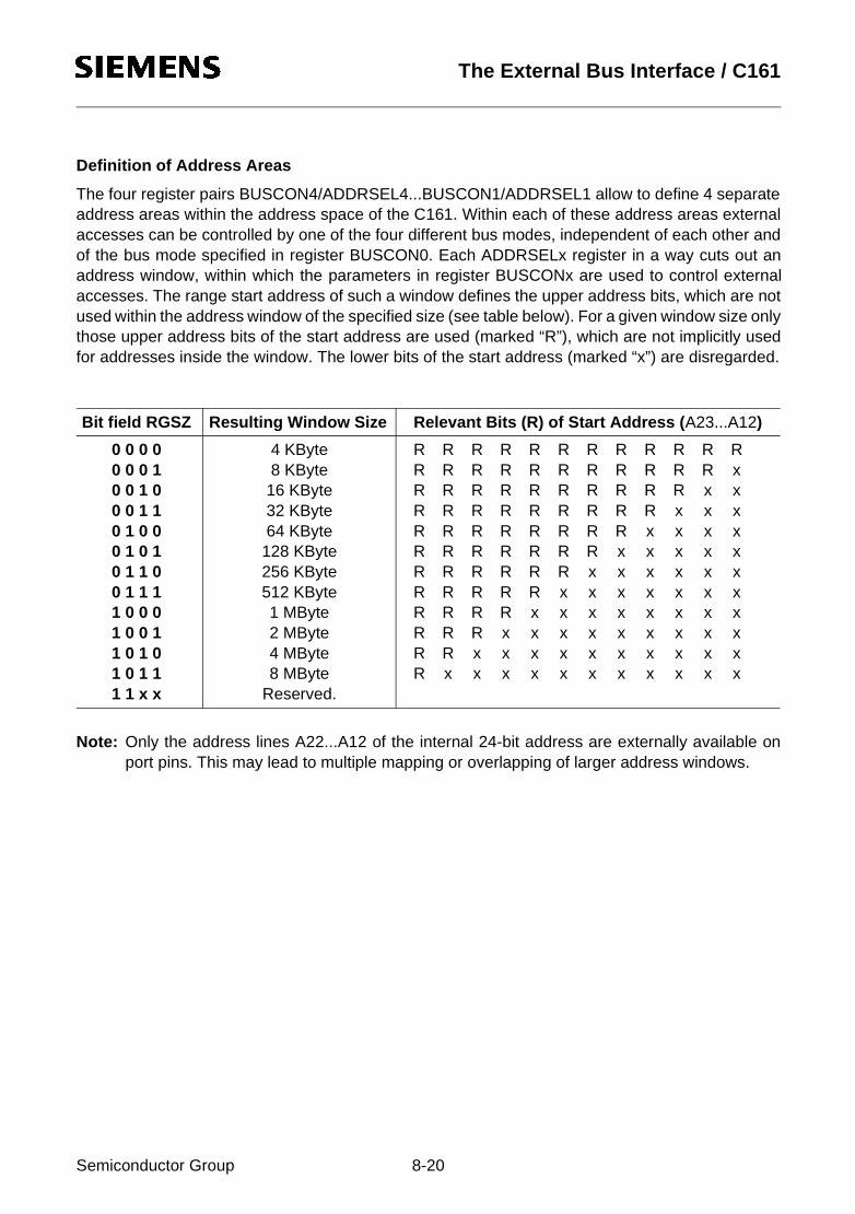
10Jul97@15:19h The External Bus Interface / C161
Definition of Address Areas
The four register pairs BUSCON4/ADDRSEL4...BUSCON1/ADDRSEL1 allow to define 4 separateaddress areas within the address space of the C161. Within each of these address areas externalaccesses can be controlled by one of the four different bus modes, independent of each other andof the bus mode specified in register BUSCON0. Each ADDRSELx register in a way cuts out anaddress window, within which the parameters in register BUSCONx are used to control externalaccesses. The range start address of such a window defines the upper address bits, which are notused within the address window of the specified size (see table below). For a given window size onlythose upper address bits of the start address are used (marked “R”), which are not implicitly usedfor addresses inside the window. The lower bits of the start address (marked “x”) are disregarded.
Note: Only the address lines A22...A12 of the internal 24-bit address are externally available onport pins. This may lead to multiple mapping or overlapping of larger address windows.
Bit field RGSZ Resulting Window Size Relevant Bits (R) of Start Address (A23...A12)
0 0 0 00 0 0 10 0 1 00 0 1 1 0 1 0 00 1 0 10 1 1 00 1 1 11 0 0 01 0 0 11 0 1 01 0 1 11 1 x x
4 KByte8 KByte
16 KByte32 KByte64 KByte
128 KByte256 KByte512 KByte1 MByte2 MByte4 MByte8 MByte
Reserved.
R R R R R R R R R R R RR R R R R R R R R R R xR R R R R R R R R R x xR R R R R R R R R x x xR R R R R R R R x x x xR R R R R R R x x x x xR R R R R R x x x x x xR R R R R x x x x x x xR R R R x x x x x x x xR R R x x x x x x x x xR R x x x x x x x x x xR x x x x x x x x x x x
Semiconductor Group 8-20

10Jul97@15:19h The External Bus Interface / C161
Address Window Arbitration
For each access the EBC compares the current address with all address select registers(programmable ADDRSELx and hardwired XADRSx). This comparison is done in four levels.
Priority 1: The hardwired XADRSx registers are evaluated first. A match with one of theseregisters directs the access to the respective X-Peripheral using the correspondingXBCONx register and ignoring all other ADDRSELx registers.
Priority 2: Registers ADDRSEL2 and ADDRSEL4 are evaluated before ADDRSEL1 and ADDRSEL3, respectively. A match with one of these registers directs the access to the respective external area using the corresponding BUSCONx register and ignoring registers ADDRSEL1/3 (see figure below).
Priority 3: A match with registers ADDRSEL1 or ADDRSEL3 directs the access to the respectiveexternal area using the corresponding XBCONx register.
Priority 4: If there is no match with any XADRSx or ADDRSELx register the access to the externalbus uses register BUSCON0.
Figure 8-10Address Window Arbitration
Note: Only the indicated overlaps are defined. All other overlaps lead to erroneous bus cycles. Eg.ADDRSEL4 may not overlap ADDRSEL2 or ADDRSEL1. The hardwired XADRSx registersare defined non-overlapping.
ActiveWindow
InactiveWindow
BUSCON0
BUSCON1
BUSCON2
XBCON0
BUSCON3
BUSCON4
Semiconductor Group 8-21

10Jul97@15:19h The External Bus Interface / C161
RP0H (F108H / 84H) SFR Reset Value: - - XXH
Note: RP0H cannot be changed via software, but rather allows to check the current configuration.
Precautions and Hints
• The external bus interface is enabled as long as at least one of the BUSCON registers has itsBUSACT bit set.
• PORT1 will output the intra-segment address as long as at least one of the BUSCON registersselects a demultiplexed external bus, even for multiplexed bus cycles.
• Not all address areas defined via registers ADDRSELx may overlap each other. The operation ofthe EBC will be unpredictable in such a case. See chapter „Address Window Arbitration“.
• The address areas defined via registers ADDRSELx may overlap internal address areas. Internalaccesses will be executed in this case.
• For any access to an internal address area the EBC will remain inactive (see EBC Idle State).
Bit Function
WRC Write Configuration0: Pins WR and BHE operate as WRL and WRH signals1: Pins WR and BHE operate as WR and BHE signals
CSSEL Chip Select Line Selection (Number of active CS outputs)0 0: 3 CS lines: CS2...CS00 1: 2 CS lines: CS1...CS01 0: No CS lines at all1 1: 4 CS lines: CS3...CS0 (Default without pulldowns)
SALSEL Segment Address Line Selection (Number of active segment address outputs)0 0: 4-bit segment address: A19...A160 1: No segment address lines at all1 0: 6-bit segment address: A21...A161 1: 2-bit segment address: A17...A16 (Default without pulldowns)
CLKCFG Clock Generation Mode ConfigurationThese pins define the clock generation mode, ie. the mechanism how the the internal CPU clock is generated from the externally applied (XTAL1) input clock.
WRC
5 4 3 2 1 011 10 9 8 7 615 14 13 12
r r- - - - r- - - -
CSSELSALSEL
r
CLKCFG
Semiconductor Group 8-22
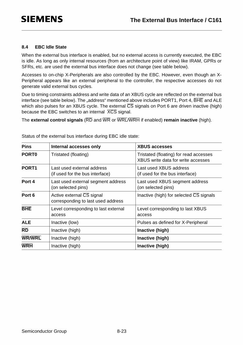
10Jul97@15:19h The External Bus Interface / C161
8.4 EBC Idle State
When the external bus interface is enabled, but no external access is currently executed, the EBCis idle. As long as only internal resources (from an architecture point of view) like IRAM, GPRs orSFRs, etc. are used the external bus interface does not change (see table below).
Accesses to on-chip X-Peripherals are also controlled by the EBC. However, even though an X-Peripheral appears like an external peripheral to the controller, the respective accesses do notgenerate valid external bus cycles.
Due to timing constraints address and write data of an XBUS cycle are reflected on the external businterface (see table below). The „address“ mentioned above includes PORT1, Port 4, BHE and ALEwhich also pulses for an XBUS cycle. The external CS signals on Port 6 are driven inactive (high)because the EBC switches to an internal XCS signal.
The external control signals (RD and WR or WRL/WRH if enabled) remain inactive (high).
Status of the external bus interface during EBC idle state:
Pins Internal accesses only XBUS accesses
PORT0 Tristated (floating) Tristated (floating) for read accessesXBUS write data for write accesses
PORT1 Last used external address(if used for the bus interface)
Last used XBUS address(if used for the bus interface)
Port 4 Last used external segment address(on selected pins)
Last used XBUS segment address(on selected pins)
Port 6 Active external CS signal corresponding to last used address
Inactive (high) for selected CS signals
BHE Level corresponding to last external access
Level corresponding to last XBUS access
ALE Inactive (low) Pulses as defined for X-Peripheral
RD Inactive (high) Inactive (high)
WR/WRL Inactive (high) Inactive (high)
WRH Inactive (high) Inactive (high)
Semiconductor Group 8-23

10Jul97@15:19h The External Bus Interface / C161
8.5 The XBUS Interface
The C161 provides an on-chip interface (the XBUS interface), which allows to connect integratedcustomer/application specific peripherals to the standard controller core. The XBUS is an internalrepresentation of the external bus interface, ie. it is operated in the same way.
The current XBUS interface is prepared to support up to 3 X-Peripherals.
For each peripheral on the XBUS (X-Peripheral) there is a separate address window controlled byan XBCON and an XADRS register. As an interface to a peripheral in many cases is represented byjust a few registers, the XADRS registers select smaller address windows than the standardADDRSEL registers. As the register pairs control integrated peripherals rather than externallyconnected ones, they are fixed by mask programming rather than being user programmable.
X-Peripheral accesses provide the same choices as external accesses, so these peripherals maybe bytewide or wordwide, with or without a separate address bus. Interrupt nodes and configurationpins (on PORT0) are provided for X-Peripherals to be integrated.
Note: If you plan to develop a peripheral of your own to be integrated into a C161 device to createa customer specific version, please ask for the specification of the XBUS interface and forfurther support.
Semiconductor Group 8-24

10Jul97@15:19h The General Purpose Timer Units / C161
9 The General Purpose Timer Units
The General Purpose Timer Units GPT1 and GPT2 represent very flexible multifunctional timerstructures which may be used for timing, event counting, pulse width measurement, pulsegeneration, frequency multiplication, and other purposes. They incorporate five 16-bit timers thatare grouped into the two timer blocks GPT1 and GPT2 (C161O only).
Block GPT1 contains 3 timers/counters with a maximum resolution of 500 ns (@ 16 MHz CPUclock), while block GPT2 contains 2 timers/counters with a maximum resolution of 250 ns(@ 16 MHz CPU clock) and a 16-bit Capture/Reload register (CAPREL). Each timer in each blockmay operate independently in a number of different modes such as gated timer or counter mode, ormay be concatenated with another timer of the same block. The auxiliary timers of GPT1 mayoptionally be configured as reload or capture registers for the core timer. In the GPT2 block, theadditional CAPREL register supports capture and reload operation with extended functionality.Each block may have alternate input/output functions and specific interrupts associated with it.
9.1 Timer Block GPT1
From a programmer’s point of view, the GPT1 block is composed of a set of SFRs as summarizedbelow. Those portions of port and direction registers which are used for alternate functions by theGPT1 block are shaded.
Figure 9-1SFRs and Port Pins Associated with Timer Block GPT1
Note: External GPT1 control is provided on the C161K and the C161O, not on the C161V.
T4IC
T2 GPT1 Timer 2 RegisterT3 GPT1 Timer 3 RegisterT4 GPT1 Timer 4 RegisterT2IC GPT1 Timer 2 Interrupt Control RegisterT3IC GPT1 Timer 3 Interrupt Control RegisterT4IC GPT1 Timer 4 Interrupt Control Register
T2IN/P3.7 T2EUD/P5.15T3IN/P3.6 T3EUD/P3.4T4IN/P3.5 T4EUD/P5.14T3OUT/P3.3
T2CON
Ports & Direction ControlAlternate Functions
Data Registers Control Registers Interrupt Control
T2 T2IC
DP3
P3
T3
T4
T3ICT3CON
T4CON
P5
ODP3
ODP3 Port 3 Open Drain Control RegisterDP3 Port 3 Direction Control RegisterP3 Port 3 Data RegisterT2CON GPT1 Timer 2 Control RegisterT3CON GPT1 Timer 3 Control RegisterT4CON GPT1 Timer 4 Control Register
Semiconductor Group 9-1
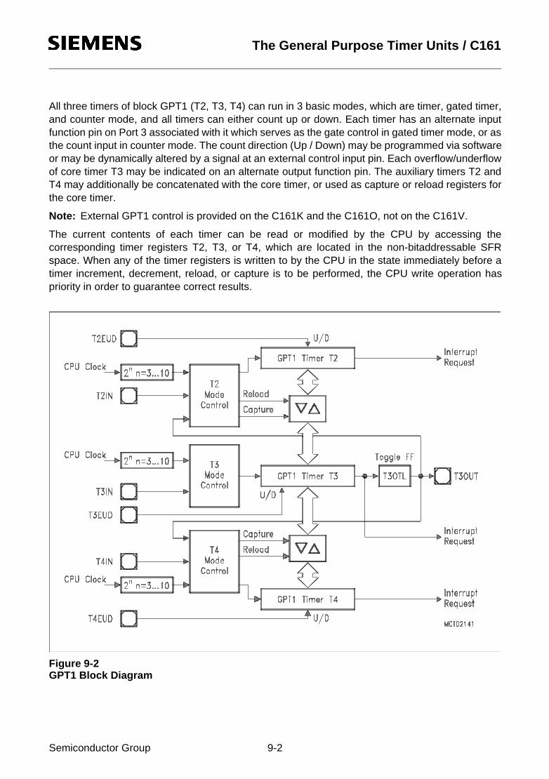
10Jul97@15:19h The General Purpose Timer Units / C161
All three timers of block GPT1 (T2, T3, T4) can run in 3 basic modes, which are timer, gated timer,and counter mode, and all timers can either count up or down. Each timer has an alternate inputfunction pin on Port 3 associated with it which serves as the gate control in gated timer mode, or asthe count input in counter mode. The count direction (Up / Down) may be programmed via softwareor may be dynamically altered by a signal at an external control input pin. Each overflow/underflowof core timer T3 may be indicated on an alternate output function pin. The auxiliary timers T2 andT4 may additionally be concatenated with the core timer, or used as capture or reload registers forthe core timer.
Note: External GPT1 control is provided on the C161K and the C161O, not on the C161V.
The current contents of each timer can be read or modified by the CPU by accessing thecorresponding timer registers T2, T3, or T4, which are located in the non-bitaddressable SFRspace. When any of the timer registers is written to by the CPU in the state immediately before atimer increment, decrement, reload, or capture is to be performed, the CPU write operation haspriority in order to guarantee correct results.
Figure 9-2GPT1 Block Diagram
Semiconductor Group 9-2

10Jul97@15:19h The General Purpose Timer Units / C161
GPT1 Core Timer T3
The core timer T3 is configured and controlled via its bitaddressable control register T3CON.
T3CON (FF42H / A1H) SFR Reset Value: 0000H
1) This function cannot be selected on the C161V.2) For the effects of bits T3UD and T3UDE refer to the direction table below.
Timer 3 Run Bit
The timer can be started or stopped by software through bit T3R (Timer T3 Run Bit). If T3R=‘0’, thetimer stops. Setting T3R to ‘1’ will start the timer.In gated timer mode, the timer will only run if T3R=‘1’ and the gate is active (high or low, asprogrammed).
Bit Function
T3I Timer 3 Input SelectionDepends on the operating mode, see respective sections.
T3M Timer 3 Mode Control (Basic Operating Mode)0 0 0 : Timer Mode0 0 1 : Counter Mode 1)
0 1 0 : Gated Timer with Gate active low 1)
0 1 1 : Gated Timer with Gate active high 1)
1 X X : Reserved. Do not use this combination.
T3R Timer 3 Run BitT3R = ‘0’: Timer / Counter 3 stopsT3R = ‘1’: Timer / Counter 3 runs
T3UD Timer 3 Up / Down Control 2)
T3UDE Timer 3 External Up/Down Enable 2)
T3OE Alternate Output Function Enable 1)
T3OE = ‘0’: Alternate Output Function DisabledT3OE = ‘1’: Alternate Output Function Enabled
T3OTL Timer 3 Output Toggle LatchToggles on each overflow / underflow of T3. Can be set or reset by software.
5 4 3 2 1 011 10 9 8 7 615 14 13 12
rw rw- rw rw rw rw rw- - - -
T3RT3UDT3OE-----T3
OTLT3
UDE T3M T3I
Semiconductor Group 9-3
10Jul97@15:19h The General Purpose Timer Units / C161
Count Direction Control
The count direction of the core timer can be controlled either by software or by the external input pinT3EUD (Timer T3 External Up/Down Control Input), which is the alternate input function of port pinP3.4. These options are selected by bits T3UD and T3UDE in control register T3CON. When the up/down control is done by software (bit T3UDE=‘0’), the count direction can be altered by setting orclearing bit T3UD. When T3UDE=‘1’, pin T3EUD is selected to be the controlling source of the countdirection. However, bit T3UD can still be used to reverse the actual count direction, as shown in thetable below. If T3UD=‘0’ and pin T3EUD shows a low level, the timer is counting up. With a highlevel at T3EUD the timer is counting down. If T3UD=‘1’, a high level at pin T3EUD specifies countingup, and a low level specifies counting down. The count direction can be changed regardless ofwhether the timer is running or not.
When pin T3EUD/P3.4 is used as external count direction control input, it must be configured asinput, ie. its corresponding direction control bit DP3.4 must be set to ‘0’.
GPT1 Core Timer T3 Count Direction Control
Note: The direction control works the same for core timer T3 and for auxiliary timers T2 and T4.Therefore the pins and bits are named Tx...External GPT1 control is provided on the C161K and the C161O, not on the C161V.
Timer 3 Output Toggle Latch
An overflow or underflow of timer T3 will clock the toggle bit T3OTL in control register T3CON.T3OTL can also be set or reset by software. Bit T3OE (Alternate Output Function Enable) in registerT3CON enables the state of T3OTL to be an alternate function of the external output pin T3OUT/P3.3. For that purpose, a ‘1’ must be written into port data latch P3.3 and pin T3OUT/P3.3 must beconfigured as output by setting direction control bit DP3.3 to ‘1’. If T3OE=‘1’, pin T3OUT thenoutputs the state of T3OTL. If T3OE=‘0’, pin T3OUT can be used as general purpose IO pin.
In addition, T3OTL can be used in conjunction with the timer over/underflows as an input for thecounter function or as a trigger source for the reload function of the auxiliary timers T2 and T4. Forthis purpose, the state of T3OTL does not have to be available at pin T3OUT, because an internalconnection is provided for this option.
Note: External GPT1 control is provided on the C161K and the C161O, not on the C161V.
Pin TxEUD Bit TxUDE Bit TxUD Count Direction
X 0 0 Count Up
X 0 1 Count Down
0 1 0 Count Up
1 1 0 Count Down
0 1 1 Count Down
1 1 1 Count Up
Semiconductor Group 9-4
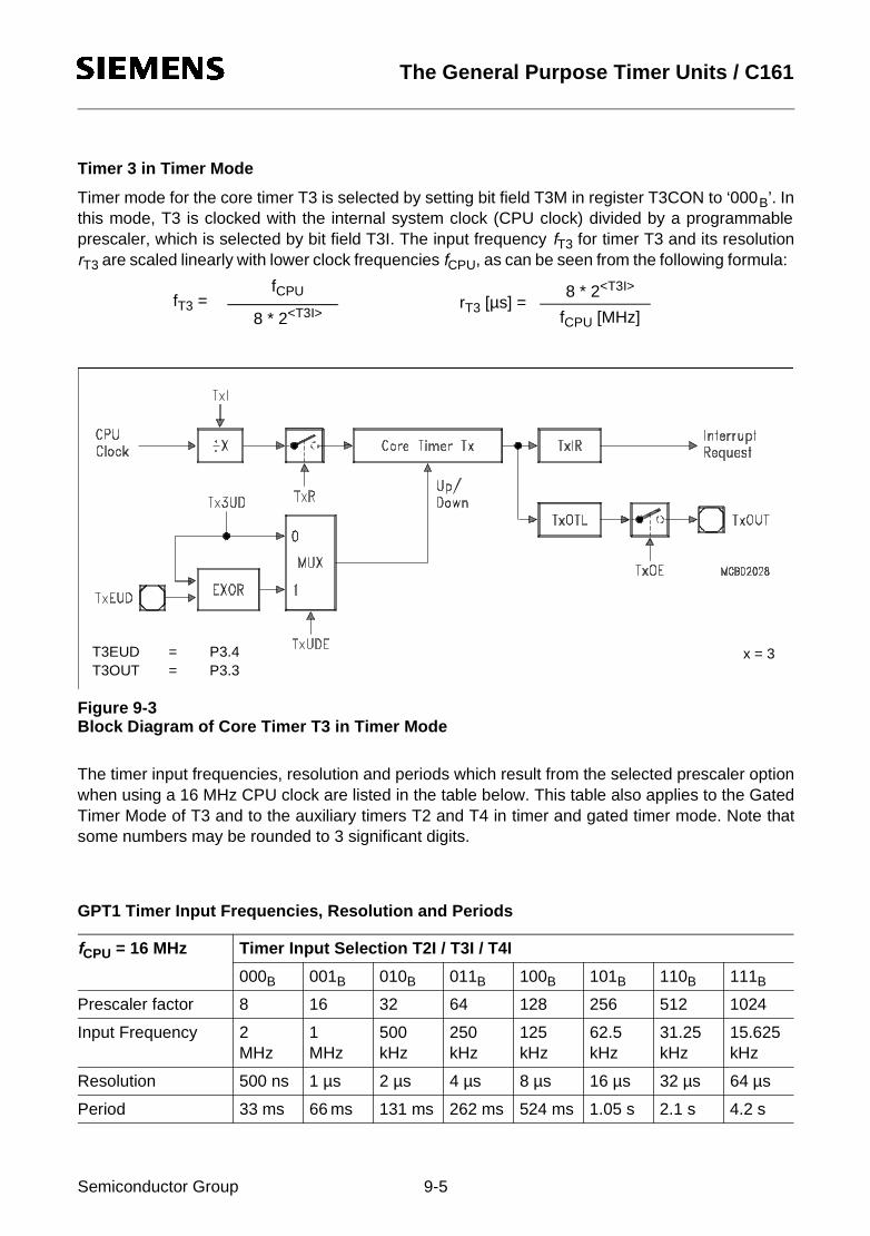
10Jul97@15:19h The General Purpose Timer Units / C161
Timer 3 in Timer Mode
Timer mode for the core timer T3 is selected by setting bit field T3M in register T3CON to ‘000B’. Inthis mode, T3 is clocked with the internal system clock (CPU clock) divided by a programmableprescaler, which is selected by bit field T3I. The input frequency fT3 for timer T3 and its resolutionrT3 are scaled linearly with lower clock frequencies fCPU, as can be seen from the following formula:
Figure 9-3Block Diagram of Core Timer T3 in Timer Mode
The timer input frequencies, resolution and periods which result from the selected prescaler optionwhen using a 16 MHz CPU clock are listed in the table below. This table also applies to the GatedTimer Mode of T3 and to the auxiliary timers T2 and T4 in timer and gated timer mode. Note thatsome numbers may be rounded to 3 significant digits.
GPT1 Timer Input Frequencies, Resolution and Periods
fCPU = 16 MHz Timer Input Selection T2I / T3I / T4I
000B 001B 010B 011B 100B 101B 110B 111B
Prescaler factor 8 16 32 64 128 256 512 1024
Input Frequency 2MHz
1MHz
500kHz
250kHz
125kHz
62.5kHz
31.25kHz
15.625kHz
Resolution 500 ns 1 µs 2 µs 4 µs 8 µs 16 µs 32 µs 64 µs
Period 33 ms 66 ms 131 ms 262 ms 524 ms 1.05 s 2.1 s 4.2 s
fT3 =fCPU
8 * 2<T3I>rT3 [µs] =
fCPU [MHz]
8 * 2<T3I>
T3EUD = P3.4T3OUT = P3.3
x = 3
Semiconductor Group 9-5

10Jul97@15:19h The General Purpose Timer Units / C161
Timer 3 in Gated Timer Mode
Gated timer mode for the core timer T3 is selected by setting bit field T3M in register T3CON to‘010B’ or ‘011B’. Bit T3M.0 (T3CON.3) selects the active level of the gate input. In gated timer modethe same options for the input frequency as for the timer mode are available. However, the inputclock to the timer in this mode is gated by the external input pin T3IN (Timer T3 External Input),which is an alternate function of P3.6.To enable this operation pin T3IN/P3.6 must be configured as input, ie. direction control bit DP3.6must contain ‘0’.
Note: External GPT1 control is provided on the C161K and the C161O, not on the C161V.
Figure 9-4Block Diagram of Core Timer T3 in Gated Timer Mode
If T3M.0=‘0’, the timer is enabled when T3IN shows a low level. A high level at this pin stops thetimer. If T3M.0=‘1’, pin T3IN must have a high level in order to enable the timer. In addition, the timercan be turned on or off by software using bit T3R. The timer will only run, if T3R=‘1’ and the gate isactive. It will stop, if either T3R=‘0’ or the gate is inactive.
Note: A transition of the gate signal at pin T3IN does not cause an interrupt request.
T3IN = P3.6T3EUD = P3.4T3OUT = P3.3
x = 3
Semiconductor Group 9-6
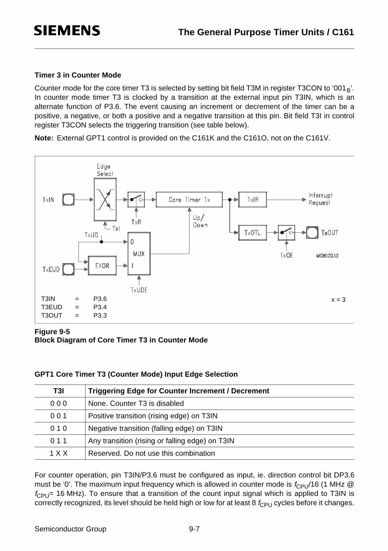
10Jul97@15:19h The General Purpose Timer Units / C161
Timer 3 in Counter Mode
Counter mode for the core timer T3 is selected by setting bit field T3M in register T3CON to ‘001B’.In counter mode timer T3 is clocked by a transition at the external input pin T3IN, which is analternate function of P3.6. The event causing an increment or decrement of the timer can be apositive, a negative, or both a positive and a negative transition at this pin. Bit field T3I in controlregister T3CON selects the triggering transition (see table below).
Note: External GPT1 control is provided on the C161K and the C161O, not on the C161V.
Figure 9-5Block Diagram of Core Timer T3 in Counter Mode
GPT1 Core Timer T3 (Counter Mode) Input Edge Selection
For counter operation, pin T3IN/P3.6 must be configured as input, ie. direction control bit DP3.6must be ‘0’. The maximum input frequency which is allowed in counter mode is fCPU/16 (1 MHz @fCPU= 16 MHz). To ensure that a transition of the count input signal which is applied to T3IN iscorrectly recognized, its level should be held high or low for at least 8 fCPU cycles before it changes.
T3I Triggering Edge for Counter Increment / Decrement
0 0 0 None. Counter T3 is disabled
0 0 1 Positive transition (rising edge) on T3IN
0 1 0 Negative transition (falling edge) on T3IN
0 1 1 Any transition (rising or falling edge) on T3IN
1 X X Reserved. Do not use this combination
T3IN = P3.6T3EUD = P3.4T3OUT = P3.3
x = 3
Semiconductor Group 9-7
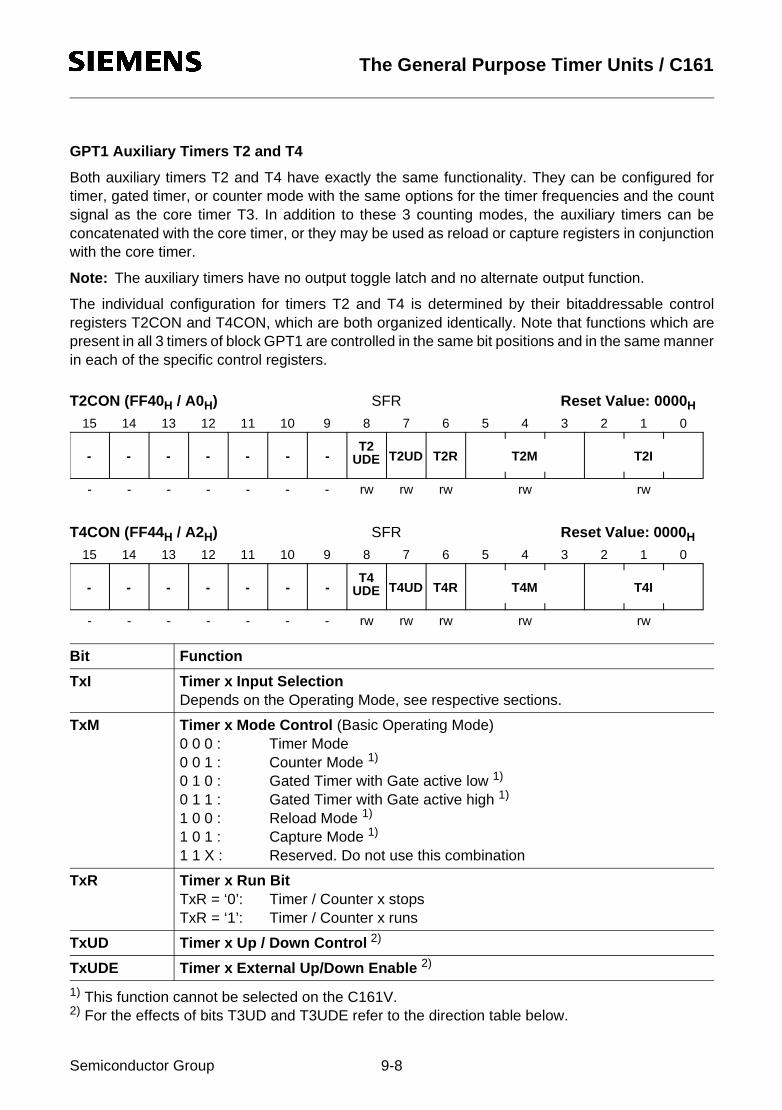
10Jul97@15:19h The General Purpose Timer Units / C161
GPT1 Auxiliary Timers T2 and T4
Both auxiliary timers T2 and T4 have exactly the same functionality. They can be configured fortimer, gated timer, or counter mode with the same options for the timer frequencies and the countsignal as the core timer T3. In addition to these 3 counting modes, the auxiliary timers can beconcatenated with the core timer, or they may be used as reload or capture registers in conjunctionwith the core timer.
Note: The auxiliary timers have no output toggle latch and no alternate output function.
The individual configuration for timers T2 and T4 is determined by their bitaddressable controlregisters T2CON and T4CON, which are both organized identically. Note that functions which arepresent in all 3 timers of block GPT1 are controlled in the same bit positions and in the same mannerin each of the specific control registers.
T2CON (FF40H / A0H) SFR Reset Value: 0000H
T4CON (FF44H / A2H) SFR Reset Value: 0000H
1) This function cannot be selected on the C161V.2) For the effects of bits T3UD and T3UDE refer to the direction table below.
Bit Function
TxI Timer x Input SelectionDepends on the Operating Mode, see respective sections.
TxM Timer x Mode Control (Basic Operating Mode)0 0 0 : Timer Mode0 0 1 : Counter Mode 1)
0 1 0 : Gated Timer with Gate active low 1)
0 1 1 : Gated Timer with Gate active high 1)
1 0 0 : Reload Mode 1)
1 0 1 : Capture Mode 1)
1 1 X : Reserved. Do not use this combination
TxR Timer x Run BitTxR = ‘0’: Timer / Counter x stopsTxR = ‘1’: Timer / Counter x runs
TxUD Timer x Up / Down Control 2)
TxUDE Timer x External Up/Down Enable 2)
5 4 3 2 1 011 10 9 8 7 615 14 13 12
rw rw- - - rw rw rw- - - -
T2RT2UD-----T2
UDE- - T2IT2M
5 4 3 2 1 011 10 9 8 7 615 14 13 12
rw rw- - - rw rw rw- - - -
T4RT4UD-----T4
UDE- - T4IT4M
Semiconductor Group 9-8

10Jul97@15:19h The General Purpose Timer Units / C161
Count Direction Control for Auxiliary Timers
The count direction of the auxiliary timers can be controlled in the same way as for the core timerT3. The description and the table apply accordingly.
Timers T2 and T4 in Timer Mode or Gated Timer Mode
When the auxiliary timers T2 and T4 are programmed to timer mode or gated timer mode, theiroperation is the same as described for the core timer T3. The descriptions, figures and tables applyaccordingly with one exception:
• There is no output toggle latch and no alternate output pin for T2 and T4.
Note: External GPT1 control is provided on the C161K and the C161O, not on the C161V.
Semiconductor Group 9-9

10Jul97@15:19h The General Purpose Timer Units / C161
Timers T2 and T4 in Counter Mode
Counter mode for the auxiliary timers T2 and T4 is selected by setting bit field TxM in the respectiveregister TxCON to ‘001B’. In counter mode timers T2 and T4 can be clocked either by a transitionat the respective external input pin TxIN, or by a transition of timer T3’s output toggle latch T3OTL.
Figure 9-6Block Diagram of an Auxiliary Timer in Counter Mode
The event causing an increment or decrement of a timer can be a positive, a negative, or both apositive and a negative transition at either the respective input pin, or at the toggle latch T3OTL.Bit field TxI in the respective control register TxCON selects the triggering transition (see tablebelow).
GPT1 Auxiliary Timer (Counter Mode) Input Edge Selection
Note: Only state transitions of T3OTL which are caused by the overflows/underflows of T3 willtrigger the counter function of T2/T4. Modifications of T3OTL via software will NOT triggerthe counter function of T2/T4.
T2I / T4I Triggering Edge for Counter Increment / Decrement
X 0 0 None. Counter Tx is disabled
0 0 1 Positive transition (rising edge) on TxIN
0 1 0 Negative transition (falling edge) on TxIN
0 1 1 Any transition (rising or falling edge) on TxIN
1 0 1 Positive transition (rising edge) of output toggle latch T3OTL
1 1 0 Negative transition (falling edge) of output toggle latch T3OTL
1 1 1 Any transition (rising or falling edge) of output toggle latch T3OTL
x = 2,4
Semiconductor Group 9-10
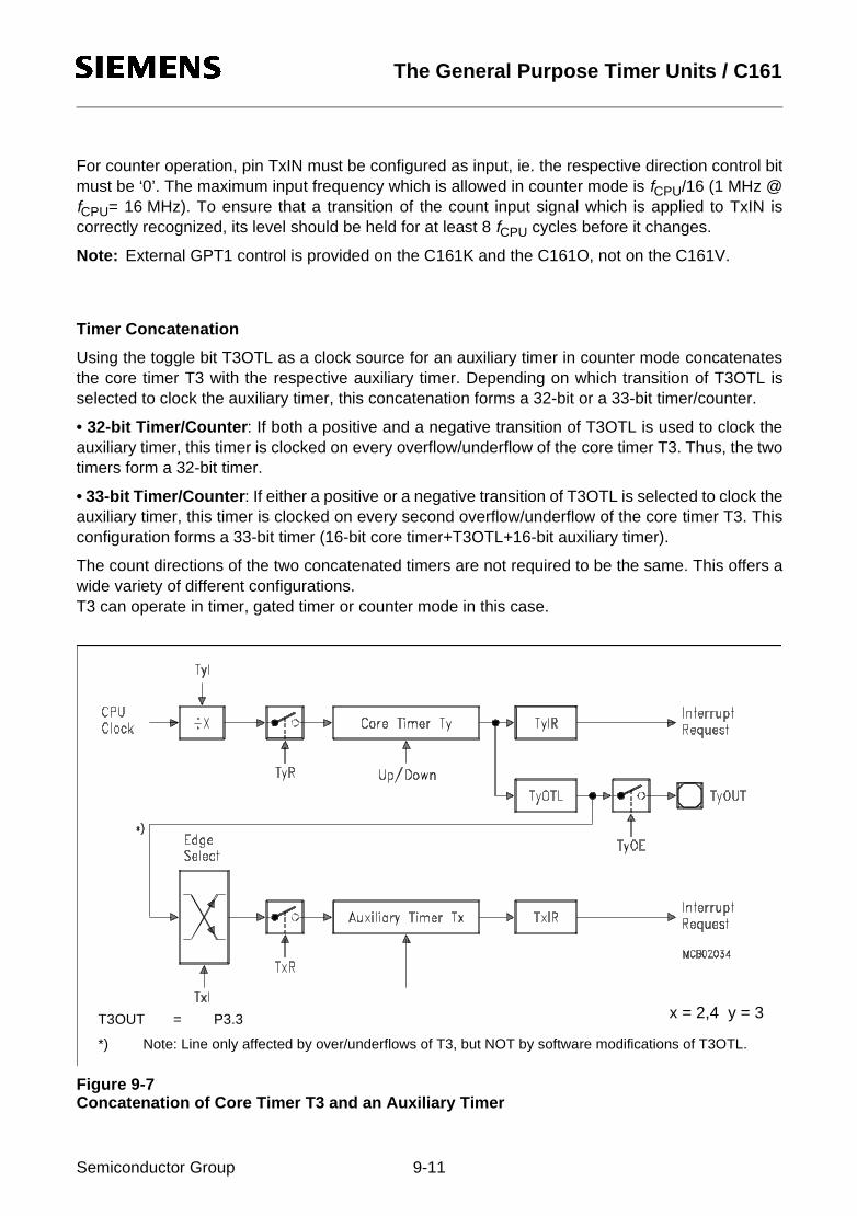
10Jul97@15:19h The General Purpose Timer Units / C161
For counter operation, pin TxIN must be configured as input, ie. the respective direction control bitmust be ‘0’. The maximum input frequency which is allowed in counter mode is fCPU/16 (1 MHz @fCPU= 16 MHz). To ensure that a transition of the count input signal which is applied to TxIN iscorrectly recognized, its level should be held for at least 8 fCPU cycles before it changes.
Note: External GPT1 control is provided on the C161K and the C161O, not on the C161V.
Timer Concatenation
Using the toggle bit T3OTL as a clock source for an auxiliary timer in counter mode concatenatesthe core timer T3 with the respective auxiliary timer. Depending on which transition of T3OTL isselected to clock the auxiliary timer, this concatenation forms a 32-bit or a 33-bit timer/counter.
• 32-bit Timer/Counter : If both a positive and a negative transition of T3OTL is used to clock theauxiliary timer, this timer is clocked on every overflow/underflow of the core timer T3. Thus, the twotimers form a 32-bit timer.
• 33-bit Timer/Counter : If either a positive or a negative transition of T3OTL is selected to clock theauxiliary timer, this timer is clocked on every second overflow/underflow of the core timer T3. Thisconfiguration forms a 33-bit timer (16-bit core timer+T3OTL+16-bit auxiliary timer).
The count directions of the two concatenated timers are not required to be the same. This offers awide variety of different configurations.T3 can operate in timer, gated timer or counter mode in this case.
Figure 9-7Concatenation of Core Timer T3 and an Auxiliary Timer
*) Note: Line only affected by over/underflows of T3, but NOT by software modifications of T3OTL.
T3OUT = P3.3 x = 2,4 y = 3
Semiconductor Group 9-11

10Jul97@15:19h The General Purpose Timer Units / C161
Auxiliary Timer in Reload Mode
Reload mode for the auxiliary timers T2 and T4 is selected by setting bit field TxM in the respectiveregister TxCON to ‘100B’. In reload mode the core timer T3 is reloaded with the contents of anauxiliary timer register, triggered by one of two different signals. The trigger signal is selected thesame way as the clock source for counter mode (see table above), ie. a transition of the auxiliarytimer’s input or the output toggle latch T3OTL may trigger the reload.
Note: When programmed for reload mode, the respective auxiliary timer (T2 or T4) stopsindependent of its run flag T2R or T4R.
Figure 9-8GPT1 Auxiliary Timer in Reload Mode
Upon a trigger signal T3 is loaded with the contents of the respective timer register (T2 or T4) andthe interrupt request flag (T2IR or T4IR) is set.
Note: When a T3OTL transition is selected for the trigger signal, also the interrupt request flag T3IRwill be set upon a trigger, indicating T3’s overflow or underflow.Modifications of T3OTL via software will NOT trigger the counter function of T2/T4.
The reload mode triggered by T3OTL can be used in a number of different configurations.Depending on the selected active transition the following functions can be performed:
• If both a positive and a negative transition of T3OTL is selected to trigger a reload, the core timerwill be reloaded with the contents of the auxiliary timer each time it overflows or underflows. This isthe standard reload mode (reload on overflow/underflow).
• If either a positive or a negative transition of T3OTL is selected to trigger a reload, the core timerwill be reloaded with the contents of the auxiliary timer on every second overflow or underflow.
*) Note: Line only affected by over/underflows of T3, but NOT by software modifications of T3OTL.
Semiconductor Group 9-12

10Jul97@15:19h The General Purpose Timer Units / C161
• Using this “single-transition” mode for both auxiliary timers allows to perform very flexible pulsewidth modulation (PWM). One of the auxiliary timers is programmed to reload the core timer on apositive transition of T3OTL, the other is programmed for a reload on a negative transition ofT3OTL. With this combination the core timer is alternately reloaded from the two auxiliary timers.
The figure below shows an example for the generation of a PWM signal using the alternate reloadmechanism. T2 defines the high time of the PWM signal (reloaded on positive transitions) and T4defines the low time of the PWM signal (reloaded on negative transitions). The PWM signal can beoutput on T3OUT with T3OE=‘1’, P3.3=‘1’ and DP3.3=‘1’. With this method the high and low time ofthe PWM signal can be varied in a wide range.
Note: The output toggle latch T3OTL is accessible via software and may be changed, if required,to modify the PWM signal. However, this will NOT trigger the reloading of T3.
Figure 9-9GPT1 Timer Reload Configuration for PWM Generation
Note: Although it is possible, it should be avoided to select the same reload trigger event for bothauxiliary timers. In this case both reload registers would try to load the core timer at the sametime. If this combination is selected, T2 is disregarded and the contents of T4 is reloaded.External GPT1 control is provided on the C161K and the C161O, not on the C161V.
*) Note: Lines only affected by over/underflows of T3, but NOT by software modifications of T3OTL.
Semiconductor Group 9-13
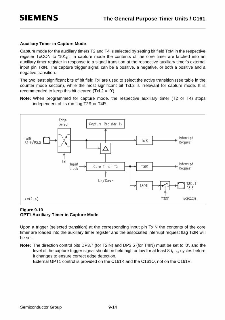
10Jul97@15:19h The General Purpose Timer Units / C161
Auxiliary Timer in Capture Mode
Capture mode for the auxiliary timers T2 and T4 is selected by setting bit field TxM in the respectiveregister TxCON to ‘101B’. In capture mode the contents of the core timer are latched into anauxiliary timer register in response to a signal transition at the respective auxiliary timer's externalinput pin TxIN. The capture trigger signal can be a positive, a negative, or both a positive and anegative transition.
The two least significant bits of bit field TxI are used to select the active transition (see table in thecounter mode section), while the most significant bit TxI.2 is irrelevant for capture mode. It isrecommended to keep this bit cleared (TxI.2 = ‘0’).
Note: When programmed for capture mode, the respective auxiliary timer (T2 or T4) stopsindependent of its run flag T2R or T4R.
Figure 9-10GPT1 Auxiliary Timer in Capture Mode
Upon a trigger (selected transition) at the corresponding input pin TxIN the contents of the coretimer are loaded into the auxiliary timer register and the associated interrupt request flag TxIR willbe set.
Note: The direction control bits DP3.7 (for T2IN) and DP3.5 (for T4IN) must be set to '0', and thelevel of the capture trigger signal should be held high or low for at least 8 fCPU cycles beforeit changes to ensure correct edge detection.External GPT1 control is provided on the C161K and the C161O, not on the C161V.
Semiconductor Group 9-14
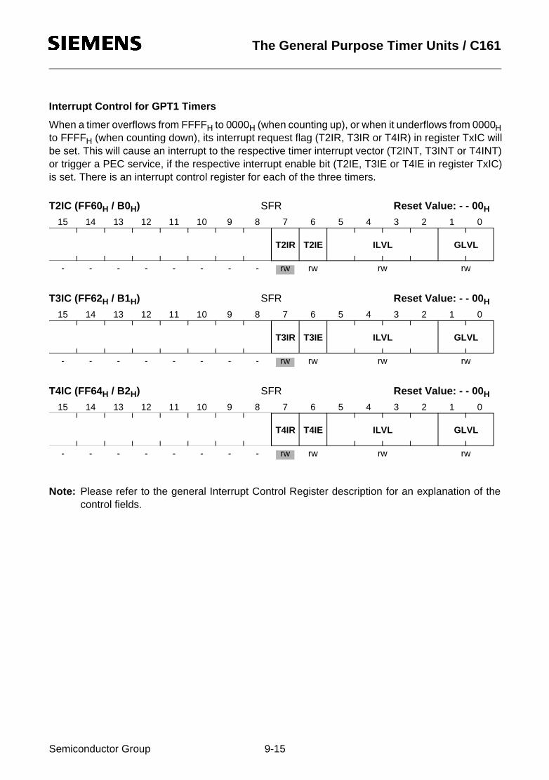
10Jul97@15:19h The General Purpose Timer Units / C161
Interrupt Control for GPT1 Timers
When a timer overflows from FFFFH to 0000H (when counting up), or when it underflows from 0000Hto FFFFH (when counting down), its interrupt request flag (T2IR, T3IR or T4IR) in register TxIC willbe set. This will cause an interrupt to the respective timer interrupt vector (T2INT, T3INT or T4INT)or trigger a PEC service, if the respective interrupt enable bit (T2IE, T3IE or T4IE in register TxIC)is set. There is an interrupt control register for each of the three timers.
T2IC (FF60H / B0H) SFR Reset Value: - - 00H
T3IC (FF62H / B1H) SFR Reset Value: - - 00H
T4IC (FF64H / B2H) SFR Reset Value: - - 00H
Note: Please refer to the general Interrupt Control Register description for an explanation of thecontrol fields.
5 4 3 2 1 011 10 9 8 7 615 14 13 12
rw rw- - - - rw rw- - - -
T2IET2IR GLVLILVL
5 4 3 2 1 011 10 9 8 7 615 14 13 12
rw rw- - - - rw rw- - - -
T3IET3IR GLVLILVL
5 4 3 2 1 011 10 9 8 7 615 14 13 12
rw rw- - - - rw rw- - - -
T4IET4IR GLVLILVL
Semiconductor Group 9-15

10Jul97@15:19h The General Purpose Timer Units / C161
9.2 Timer Block GPT2
From a programmer’s point of view, the GPT2 block is represented by a set of SFRs as summarizedbelow. Those portions of port and direction registers which are used for alternate functions by theGPT2 block are shaded.
Figure 9-11SFRs and Port Pins Associated with Timer Block GPT2
Note: GPT2 is only provided on the C161O.
Timer block GPT2 supports high precision event control with a maximum resolution of 250 ns (@16 MHz CPU clock). It includes the two timers T5 and T6, and the 16-bit capture/reload registerCAPREL. Timer T6 is referred to as the core timer, and T5 is referred to as the auxiliary timer ofGPT2.
The count direction (Up / Down) may be programmed via software. An overflow/underflow of T6 isindicated by the output toggle bit T6OTL. In addition, T6 may be reloaded with the contents ofCAPREL.
The toggle bit supports the concatenation of T6 with auxiliary timer T5. Triggered by an externalsignal, the contents of T5 can be captured into register CAPREL, and T5 may optionally be cleared.Both timer T6 and T5 can count up or down, and the current timer value can be read or modified bythe CPU in the non-bitaddressable SFRs T5 and T6.
ODP3 Port 3 Open Drain Control RegisterDP3 Port 3 Direction Control RegisterP3 Port 3 Data RegisterT5CON GPT2 Timer 5 Control RegisterT6CON GPT2 Timer 6 Control Register
CAPIN/P3.2
T5CON
Control Registers
T5 GPT2 Timer 5 RegisterT6 GPT2 Timer 6 RegisterCAPREL GPT2 Capture/Reload RegisterT5IC GPT2 Timer 5 Interrupt Control RegisterT6IC GPT2 Timer 6 Interrupt Control RegisterCRIC GPT2 CAPREL Interrupt Control Register
Ports & Direction ControlAlternate Functions
Data Registers Control Registers Interrupt Control
T5 T5IC
DP3
P3
T6
CAPREL
T6IC
CRIC
T6CON
ODP3 E
Semiconductor Group 9-16
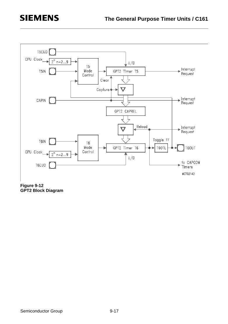
10Jul97@15:19h The General Purpose Timer Units / C161
Figure 9-12GPT2 Block Diagram
Semiconductor Group 9-17

10Jul97@15:19h The General Purpose Timer Units / C161
GPT2 Core Timer T6
The operation of the core timer T6 is controlled by its bitaddressable control register T6CON.
T6CON (FF48H / A4H) SFR Reset Value: 0000H
Timer 6 Run Bit
The timer can be started or stopped by software through bit T6R (Timer T6 Run Bit). If T6R=‘0’, thetimer stops. Setting T6R to ‘1’ will start the timer.
Count Direction Control
The count direction of the core timer can be controlled via software by setting or clearing bit T6UD.The count direction can be changed regardless of whether the timer is running or not.
Timer 6 Output Toggle Latch
An overflow or underflow of timer T6 will clock the toggle bit T6OTL in control register T6CON.T6OTL can also be set or reset by software. T6OTL can be used in conjunction with the timer over/underflows as an input for the counter function of the auxiliary timer T5.
Bit Function
T6I Timer 6 Input SelectionDepends on the Operating Mode, see below.
T6M Timer 6 Mode Control (Basic Operating Mode)0 0 0 : Timer ModeNote: The other combinations of T6M are reserved
and lead to undefined behaviour if selected.
T6R Timer 6 Run BitT6R = ‘0’: Timer / Counter 6 stopsT6R = ‘1’: Timer / Counter 6 runs
T6UD Timer 6 Up / Down Control
T6OTL Timer 6 Output Toggle LatchToggles on each overflow / underflow of T6. Can be set or reset by software.
T6SR Timer 6 Reload Mode EnableT6SR = ‘0’: Reload from register CAPREL DisabledT6SR = ‘1’: Reload from register CAPREL Enabled
- -
5 4 3 2 1 011 10 9 8 7 615 14 13 12
rw rw- rw - - rw rwrw - - -
T6RT6UD----T6SRT6
OTL T6IT6M
Semiconductor Group 9-18
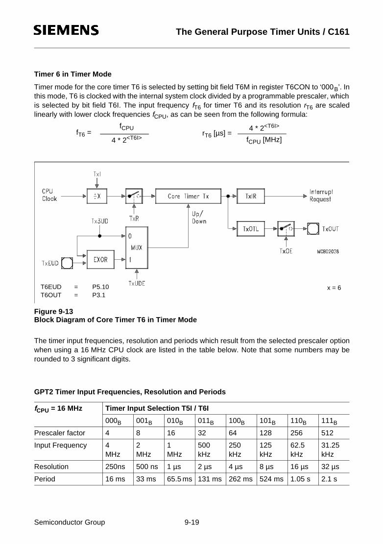
10Jul97@15:19h The General Purpose Timer Units / C161
Timer 6 in Timer Mode
Timer mode for the core timer T6 is selected by setting bit field T6M in register T6CON to ‘000B’. Inthis mode, T6 is clocked with the internal system clock divided by a programmable prescaler, whichis selected by bit field T6I. The input frequency fT6 for timer T6 and its resolution rT6 are scaledlinearly with lower clock frequencies fCPU, as can be seen from the following formula:
Figure 9-13Block Diagram of Core Timer T6 in Timer Mode
The timer input frequencies, resolution and periods which result from the selected prescaler optionwhen using a 16 MHz CPU clock are listed in the table below. Note that some numbers may berounded to 3 significant digits.
GPT2 Timer Input Frequencies, Resolution and Periods
fCPU = 16 MHz Timer Input Selection T5I / T6I
000B 001B 010B 011B 100B 101B 110B 111B
Prescaler factor 4 8 16 32 64 128 256 512
Input Frequency 4MHz
2MHz
1MHz
500kHz
250kHz
125kHz
62.5kHz
31.25kHz
Resolution 250ns 500 ns 1 µs 2 µs 4 µs 8 µs 16 µs 32 µs
Period 16 ms 33 ms 65.5 ms 131 ms 262 ms 524 ms 1.05 s 2.1 s
fT6 =fCPU
4 * 2<T6I>rT6 [µs] =
fCPU [MHz]
4 * 2<T6I>
T6EUD = P5.10T6OUT = P3.1
x = 6
Semiconductor Group 9-19

10Jul97@15:19h The General Purpose Timer Units / C161
GPT2 Auxiliary Timer T5
The auxiliary timer T5 can be configured for timer mode with the same options for the timerfrequencies as the core timer T6. In addition the auxiliary timer can be concatenated with the coretimer.
Note: The auxiliary timer has no output toggle latch.
The individual configuration for timer T5 is determined by its bitaddressable control register T5CON.Note that functions which are present in both timers of block GPT2 are controlled in the same bitpositions and in the same manner in each of the specific control registers.
T5CON (FF46H / A3H) SFR Reset Value: 0000H
Bit Function
T5I Timer 5 Input SelectionDepends on the Operating Mode, see below.
T5M Timer 5 Mode Control (Basic Operating Mode)0 0 : Timer ModeNote: The other combinations of T5M are reserved
and lead to undefined behaviour if selected.
T5R Timer 5 Run BitT5R = ‘0’: Timer / Counter 5 stopsT5R = ‘1’: Timer / Counter 5 runs
T5UD Timer 5 Up / Down Control
CI Register CAPREL Input Selection0 0 : Capture disabled0 1 : Positive transition (rising edge) on CAPIN1 0 : Negative transition (falling edge) on CAPIN1 1 : Any transition (rising or falling edge) on CAPIN
T5CLR Timer 5 Clear BitT5CLR = ‘0’: Timer 5 not cleared on a captureT5CLR = ‘1’: Timer 5 is cleared on a capture
T5SC Timer 5 Capture Mode EnableT5SC = ‘0’: Capture into register CAPREL DisabledT5SC = ‘1’: Capture into register CAPREL Enabled
-- -T5SCT5
CLR T5UD T5R- -
5 4 3 2 1 011 10 9 8 7 615 14 13 12
- rw rw- - - - rw rwrw rw rw
T5IT5MCI
Semiconductor Group 9-20
10Jul97@15:19h The General Purpose Timer Units / C161
Count Direction Control for Auxiliary Timer
The count direction of the auxiliary timer can be controlled in the same way as for the core timer T6.The description applies accordingly.
Timer T5 in Timer Mode
When the auxiliary timer T5 is programmed to timer mode its operation is the same as described forthe core timer T6. The descriptions, figures and tables apply accordingly with one exception:
• There is no output toggle latch for T5.
Timer Concatenation
Using the toggle bit T6OTL as a clock source for the auxiliary timer in counter mode concatenatesthe core timer T6 with the auxiliary timer. Depending on which transition of T6OTL is selected toclock the auxiliary timer, this concatenation forms a 32-bit or a 33-bit timer / counter.
• 32-bit Timer/Counter : If both a positive and a negative transition of T6OTL is used to clock theauxiliary timer, this timer is clocked on every overflow/underflow of the core timer T6. Thus, the twotimers form a 32-bit timer.
• 33-bit Timer/Counter : If either a positive or a negative transition of T6OTL is selected to clock theauxiliary timer, this timer is clocked on every second overflow/underflow of the core timer T6. Thisconfiguration forms a 33-bit timer (16-bit core timer+T6OTL+16-bit auxiliary timer).
The count directions of the two concatenated timers are not required to be the same. This offers awide variety of different configurations.
Semiconductor Group 9-21
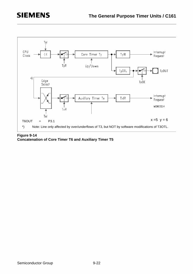
10Jul97@15:19h The General Purpose Timer Units / C161
Figure 9-14Concatenation of Core Timer T6 and Auxiliary Timer T5
*) Note: Line only affected by over/underflows of T3, but NOT by software modifications of T3OTL.
T6OUT = P3.1 x =5 y = 6
Semiconductor Group 9-22

10Jul97@15:19h The General Purpose Timer Units / C161
GPT2 Capture/Reload Register CAPREL in Capture Mode
This 16-bit register can be used as a capture register for the auxiliary timer T5. This mode isselected by setting bit T5SC=‘1’ in control register T5CON. The source for a capture trigger is theexternal input pin CAPIN, which is an alternate input function of port pin P3.2. Either a positive, anegative, or both a positive and a negative transition at this pin can be selected to trigger the capturefunction. The active edge is controlled by bit field CI in register T5CON. The same coding is usedas in the two least significant bits of bit field T5I (see table in counter mode section).
The maximum input frequency for the capture trigger signal at CAPIN is fCPU/4 (2 MHz @ fCPU=16 MHz). To ensure that a transition of the capture trigger signal is correctly recognized, its levelshould be held for at least 4 fCPU cycles before it changes.
When a selected transition at the external input pin CAPIN is detected, the contents of the auxiliarytimer T5 are latched into register CAPREL, and interrupt request flag CRIR is set. With the sameevent, timer T5 can be cleared to 0000H. This option is controlled by bit T5CLR in register T5CON.If T5CLR=‘0’, the contents of timer T5 are not affected by a capture. If T5CLR=‘1’, timer T5 iscleared after the current timer value has been latched into register CAPREL.
Note: Bit T5SC only controls whether a capture is performed or not. If T5SC=‘0’, the input pinCAPIN can still be used to clear timer T5 or as an external interrupt input. This interrupt iscontrolled by the CAPREL interrupt control register CRIC.
Figure 9-15GPT2 Register CAPREL in Capture Mode
Semiconductor Group 9-23

10Jul97@15:19h The General Purpose Timer Units / C161
GPT2 Capture/Reload Register CAPREL in Reload Mode
This 16-bit register can be used as a reload register for the core timer T6. This mode is selected bysetting bit T6SR=‘1’ in register T6CON. The event causing a reload in this mode is an overflow orunderflow of the core timer T6.
When timer T6 overflows from FFFFH to 0000H (when counting up) or when it underflows from0000H to FFFFH (when counting down), the value stored in register CAPREL is loaded into timer T6.This will not set the interrupt request flag CRIR associated with the CAPREL register. However,interrupt request flag T6IR will be set indicating the overflow/underflow of T6.
Figure 9-16GPT2 Register CAPREL in Reload Mode
Semiconductor Group 9-24

10Jul97@15:19h The General Purpose Timer Units / C161
GPT2 Capture/Reload Register CAPREL in Capture-And-Reload Mode
Since the reload function and the capture function of register CAPREL can be enabled individuallyby bits T5SC and T6SR, the two functions can be enabled simultaneously by setting both bits. Thisfeature can be used to generate an output frequency that is a multiple of the input frequency.
Figure 9-17GPT2 Register CAPREL in Capture-And-Reload Mode
This combined mode can be used to detect consecutive external events which may occuraperiodically, but where a finer resolution, that means, more ’ticks’ within the time between twoexternal events is required.
For this purpose, the time between the external events is measured using timer T5 and the CAPRELregister. Timer T5 runs in timer mode counting up with a frequency of eg. fCPU/32. The externalevents are applied to pin CAPIN. When an external event occurs, the timer T5 contents are latchedinto register CAPREL, and timer T5 is cleared (T5CLR=‘1’). Thus, register CAPREL alwayscontains the correct time between two events, measured in timer T5 increments. Timer T6, whichruns in timer mode counting down with a frequency of eg. fCPU/4, uses the value in register CAPREL
Semiconductor Group 9-25
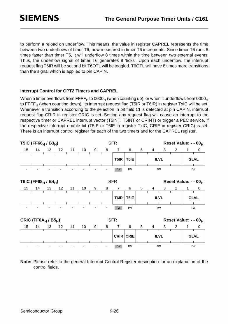
10Jul97@15:19h The General Purpose Timer Units / C161
to perform a reload on underflow. This means, the value in register CAPREL represents the timebetween two underflows of timer T6, now measured in timer T6 increments. Since timer T6 runs 8times faster than timer T5, it will underflow 8 times within the time between two external events.Thus, the underflow signal of timer T6 generates 8 ’ticks’. Upon each underflow, the interruptrequest flag T6IR will be set and bit T6OTL will be toggled. T6OTL will have 8 times more transitionsthan the signal which is applied to pin CAPIN.
Interrupt Control for GPT2 Timers and CAPREL
When a timer overflows from FFFFH to 0000H (when counting up), or when it underflows from 0000Hto FFFFH (when counting down), its interrupt request flag (T5IR or T6IR) in register TxIC will be set.Whenever a transition according to the selection in bit field CI is detected at pin CAPIN, interruptrequest flag CRIR in register CRIC is set. Setting any request flag will cause an interrupt to therespective timer or CAPREL interrupt vector (T5INT, T6INT or CRINT) or trigger a PEC service, ifthe respective interrupt enable bit (T5IE or T6IE in register TxIC, CRIE in register CRIC) is set.There is an interrupt control register for each of the two timers and for the CAPREL register.
T5IC (FF66H / B3H) SFR Reset Value: - - 00H
T6IC (FF68H / B4H) SFR Reset Value: - - 00H
CRIC (FF6AH / B5H) SFR Reset Value: - - 00H
Note: Please refer to the general Interrupt Control Register description for an explanation of thecontrol fields.
5 4 3 2 1 011 10 9 8 7 615 14 13 12
rw rw- - - - rw rw- - - -
T5IET5IR GLVLILVL
5 4 3 2 1 011 10 9 8 7 615 14 13 12
rw rw- - - - rw rw- - - -
T6IET6IR GLVLILVL
5 4 3 2 1 011 10 9 8 7 615 14 13 12
rw rw- - - - rw rw- - - -
CRIECRIR GLVLILVL
Semiconductor Group 9-26

10Jul97@15:19hThe Asynchronous/Synchr. Serial Interface / C161
10 The Asynchronous/Synchr. Serial Interface
The Asynchronous/Synchronous Serial Interface ASC0 provides serial communication between theC161 and other microcontrollers, microprocessors or external peripherals.
The ASC0 supports full-duplex asynchronous communication up to 500 KBaud and half-duplexsynchronous communication up to 2 MBaud (@ 16 MHz CPU clock). In synchronous mode, dataare transmitted or received synchronous to a shift clock which is generated by the C161. Inasynchronous mode, 8- or 9-bit data transfer, parity generation, and the number of stop bits can beselected. Parity, framing, and overrun error detection is provided to increase the reliability of datatransfers. Transmission and reception of data is double-buffered. For multiprocessorcommunication, a mechanism to distinguish address from data bytes is included. Testing issupported by a loop-back option. A 13-bit baud rate generator provides the ASC0 with a separateserial clock signal.
Figure 10-1SFRs and Port Pins associated with ASC0
The operating mode of the serial channel ASC0 is controlled by its bitaddressable control registerS0CON. This register contains control bits for mode and error check selection, and status flags forerror identification.
S0TIC
S0TBIC ERXD0 / P3.11TXD0 / P3.10
ODP3 Port 3 Open Drain Control RegisterDP3 Port 3 Direction Control RegisterS0BG ASC0 Baud Rate Generator/Reload RegisterS0TBUF ASC0 Transmit Buffer RegisterS0TIC ASC0 Transmit Interrupt Control RegisterS0TBIC ASC0 Transmit Buffer Interrupt Control Reg.
P3 Port 3 Data RegisterS0CON ASC0 Control RegisterS0RBUF ASC0 Receive Buffer Register (read only)S0RIC ASC0 Receive Interrupt Control RegisterS0EIC ASC0 Error Interrupt Control Register
ODP3 E
Ports & Direction ControlAlternate Functions
Data Registers Control Registers Interrupt Control
S0BG S0CON
DP3
P3
S0TBUF
S0RBUF
S0RIC
S0EIC
Semiconductor Group 10-1

10Jul97@15:19hThe Asynchronous/Synchr. Serial Interface / C161
S0CON (FFB0H / D8H) SFR Reset Value: 0000H
Bit Function
S0M ASC0 Mode Control0 0 0 : 8-bit data synchronous operation0 0 1 : 8-bit data async. operation0 1 0 : Reserved. Do not use this combination!0 1 1 : 7-bit data + parity async. operation1 0 0 : 9-bit data async. operation1 0 1 : 8-bit data + wake up bit async. operation1 1 0 : Reserved. Do not use this combination!1 1 1 : 8-bit data + parity async. operation
S0STP Number of Stop Bits Selection async. operation0 : One stop bit1 : Two stop bits
S0REN Receiver Enable Bit0 : Receiver disabled1 : Receiver enabled
(Reset by hardware after reception of byte in synchronous mode)
S0PEN Parity Check Enable Bit async. operation0 : Ignore parity1 : Check parity
S0FEN Framing Check Enable Bit async. operation0 : Ignore framing errors1 : Check framing errors
S0OEN Overrun Check Enable Bit0 : Ignore overrun errors1 : Check overrun errors
S0PE Parity Error FlagSet by hardware on a parity error (S0PEN=’1’). Must be reset by software.
S0FE Framing Error FlagSet by hardware on a framing error (S0FEN=’1’). Must be reset by software.
S0OE Overrun Error FlagSet by hardware on an overrun error (S0OEN=’1’). Must be reset by software.
S0ODD Parity Selection Bit0 : Even parity (parity bit set on odd number of ‘1’s in data)1 : Odd parity (parity bit set on even number of ‘1’s in data)
S0FE
5 4 3 2 1 011 10 9 8 7 615 14 13 12
rw rw rw rw- rw rw rwrw rw rw rw
-S0LBS0R S0PES0
STPS0
RENS0
PENS0
FENS0
OEN
rw rw
S0OES0
ODDS0
BRS S0M
Semiconductor Group 10-2

10Jul97@15:19hThe Asynchronous/Synchr. Serial Interface / C161
A transmission is started by writing to the Transmit Buffer register S0TBUF (via an instruction or aPEC data transfer). Only the number of data bits which is determined by the selected operatingmode will actually be transmitted, ie. bits written to positions 9 through 15 of register S0TBUF arealways insignificant. After a transmission has been completed, the transmit buffer register is clearedto 0000H.Data transmission is double-buffered, so a new character may be written to the transmit bufferregister, before the transmission of the previous character is complete. This allows the transmissionof characters back-to-back without gaps.
Data reception is enabled by the Receiver Enable Bit S0REN. After reception of a character hasbeen completed, the received data and, if provided by the selected operating mode, the receivedparity bit can be read from the (read-only) Receive Buffer register S0RBUF. Bits in the upper half ofS0RBUF which are not valid in the selected operating mode will be read as zeros.Data reception is double-buffered, so that reception of a second character may already begin beforethe previously received character has been read out of the receive buffer register. In all modes,receive buffer overrun error detection can be selected through bit S0OEN. When enabled, theoverrun error status flag S0OE and the error interrupt request flag S0EIR will be set when thereceive buffer register has not been read by the time reception of a second character is complete.The previously received character in the receive buffer is overwritten.
The Loop-Back option (selected by bit S0LB) allows the data currently being transmitted to bereceived simultaneously in the receive buffer. This may be used to test serial communicationroutines at an early stage without having to provide an external network. In loop-back mode thealternate input/output functions of the Port 3 pins are not necessary.
Note: Serial data transmission or reception is only possible when the Baud Rate Generator Run BitS0R is set to ‘1’. Otherwise the serial interface is idle.Do not program the mode control field S0M in register S0CON to one of the reservedcombinations to avoid unpredictable behaviour of the serial interface.
S0BRS Baudrate Selection Bit0 : Divide clock by reload-value + constant (depending on mode)1 : Additionally reduce serial clock to 2/3rd
S0LB LoopBack Mode Enable Bit0 : Standard transmit/receive mode1 : Loopback mode enabled
S0R Baudrate Generator Run Bit0 : Baudrate generator disabled (ASC0 inactive)1 : Baudrate generator enabled
Bit Function
Semiconductor Group 10-3
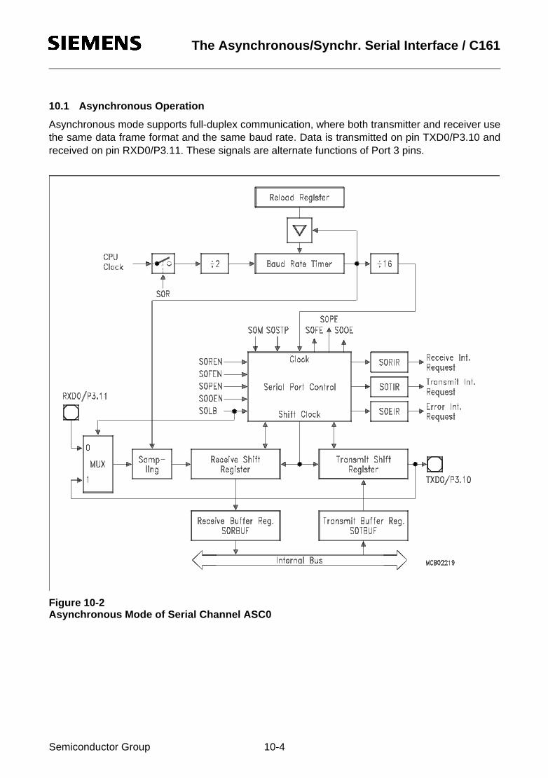
10Jul97@15:19hThe Asynchronous/Synchr. Serial Interface / C161
10.1 Asynchronous Operation
Asynchronous mode supports full-duplex communication, where both transmitter and receiver usethe same data frame format and the same baud rate. Data is transmitted on pin TXD0/P3.10 andreceived on pin RXD0/P3.11. These signals are alternate functions of Port 3 pins.
Figure 10-2Asynchronous Mode of Serial Channel ASC0
Semiconductor Group 10-4
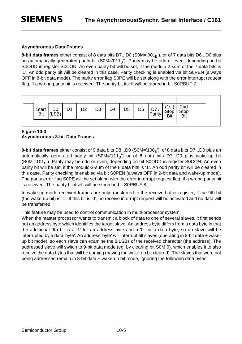
10Jul97@15:19hThe Asynchronous/Synchr. Serial Interface / C161
Asynchronous Data Frames
8-bit data frames either consist of 8 data bits D7...D0 (S0M=’001B’), or of 7 data bits D6...D0 plusan automatically generated parity bit (S0M=’011B’). Parity may be odd or even, depending on bitS0ODD in register S0CON. An even parity bit will be set, if the modulo-2-sum of the 7 data bits is‘1’. An odd parity bit will be cleared in this case. Parity checking is enabled via bit S0PEN (alwaysOFF in 8-bit data mode). The parity error flag S0PE will be set along with the error interrupt requestflag, if a wrong parity bit is received. The parity bit itself will be stored in bit S0RBUF.7.
Figure 10-3Asynchronous 8-bit Data Frames
9-bit data frames either consist of 9 data bits D8...D0 (S0M=’100B’), of 8 data bits D7...D0 plus anautomatically generated parity bit (S0M=’111B’) or of 8 data bits D7...D0 plus wake-up bit(S0M=’101B’). Parity may be odd or even, depending on bit S0ODD in register S0CON. An evenparity bit will be set, if the modulo-2-sum of the 8 data bits is ‘1’. An odd parity bit will be cleared inthis case. Parity checking is enabled via bit S0PEN (always OFF in 9-bit data and wake-up mode).The parity error flag S0PE will be set along with the error interrupt request flag, if a wrong parity bitis received. The parity bit itself will be stored in bit S0RBUF.8.
In wake-up mode received frames are only transferred to the receive buffer register, if the 9th bit(the wake-up bit) is ‘1’. If this bit is ‘0’, no receive interrupt request will be activated and no data willbe transferred.
This feature may be used to control communication in multi-processor system:When the master processor wants to transmit a block of data to one of several slaves, it first sendsout an address byte which identifies the target slave. An address byte differs from a data byte in thatthe additional 9th bit is a '1' for an address byte and a '0' for a data byte, so no slave will beinterrupted by a data 'byte'. An address 'byte' will interrupt all slaves (operating in 8-bit data + wake-up bit mode), so each slave can examine the 8 LSBs of the received character (the address). Theaddressed slave will switch to 9-bit data mode (eg. by clearing bit S0M.0), which enables it to alsoreceive the data bytes that will be coming (having the wake-up bit cleared). The slaves that were notbeing addressed remain in 8-bit data + wake-up bit mode, ignoring the following data bytes.
2ndStopBit
StartBit
D0(LSB)
D1 D2 D3 D4 D5 D6 D7 /Parity
(1st)StopBit
Semiconductor Group 10-5
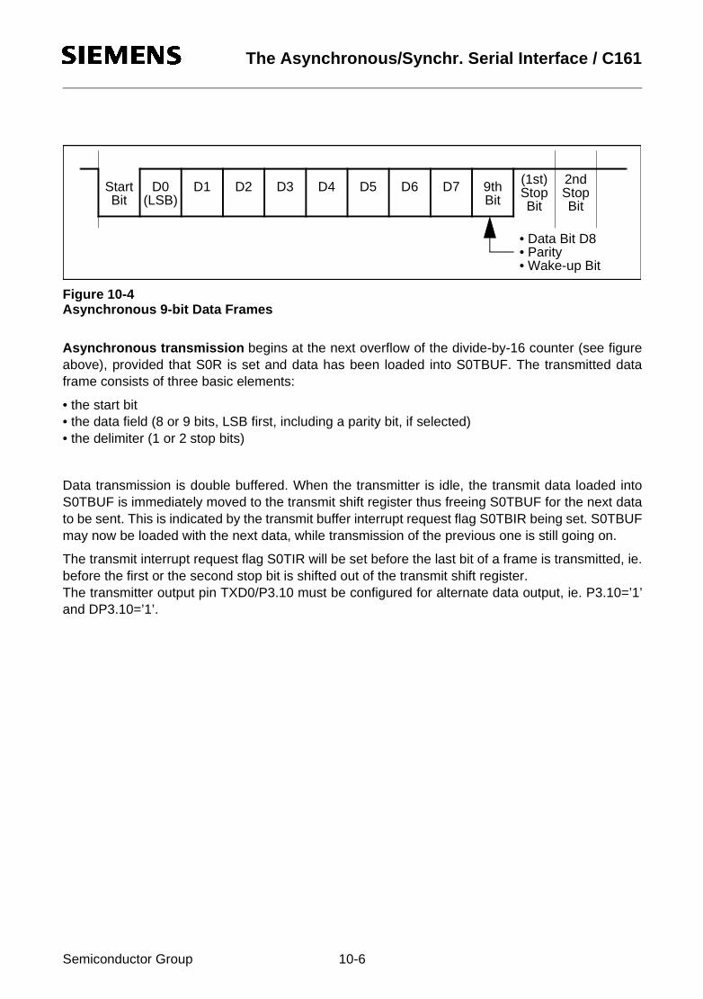
10Jul97@15:19hThe Asynchronous/Synchr. Serial Interface / C161
Figure 10-4Asynchronous 9-bit Data Frames
Asynchronous transmission begins at the next overflow of the divide-by-16 counter (see figureabove), provided that S0R is set and data has been loaded into S0TBUF. The transmitted dataframe consists of three basic elements:
• the start bit• the data field (8 or 9 bits, LSB first, including a parity bit, if selected)• the delimiter (1 or 2 stop bits)
Data transmission is double buffered. When the transmitter is idle, the transmit data loaded intoS0TBUF is immediately moved to the transmit shift register thus freeing S0TBUF for the next datato be sent. This is indicated by the transmit buffer interrupt request flag S0TBIR being set. S0TBUFmay now be loaded with the next data, while transmission of the previous one is still going on.
The transmit interrupt request flag S0TIR will be set before the last bit of a frame is transmitted, ie.before the first or the second stop bit is shifted out of the transmit shift register.The transmitter output pin TXD0/P3.10 must be configured for alternate data output, ie. P3.10=’1’and DP3.10=’1’.
2ndStopBit
StartBit
D0(LSB)
D1 D2 D3 D4 D5 D6 9thBit
(1st)StopBit
D7
• Data Bit D8• Parity• Wake-up Bit
Semiconductor Group 10-6
10Jul97@15:19hThe Asynchronous/Synchr. Serial Interface / C161
Asynchronous reception is initiated by a falling edge (1-to-0 transition) on pin RXD0, providedthat bits S0R and S0REN are set. The receive data input pin RXD0 is sampled at 16 times the rateof the selected baud rate. A majority decision of the 7th, 8th and 9th sample determines the effectivebit value. This avoids erroneous results that may be caused by noise.
If the detected value is not a ’0’ when the start bit is sampled, the receive circuit is reset and waitsfor the next 1-to-0 transition at pin RXD0. If the start bit proves valid, the receive circuit continuessampling and shifts the incoming data frame into the receive shift register.
When the last stop bit has been received, the content of the receive shift register is transferred tothe receive data buffer register S0RBUF. Simultaneously, the receive interrupt request flag S0RIRis set after the 9th sample in the last stop bit time slot (as programmed), regardless whether validstop bits have been received or not. The receive circuit then waits for the next start bit (1-to-0transition) at the receive data input pin.
The receiver input pin RXD0/P3.11 must be configured for input, ie. DP3.11=’0’.
Asynchronous reception is stopped by clearing bit S0REN. A currently received frame is completedincluding the generation of the receive interrupt request and an error interrupt request, ifappropriate. Start bits that follow this frame will not be recognized.
Note: In wake-up mode received frames are only transferred to the receive buffer register, if the 9thbit (the wake-up bit) is ‘1’. If this bit is ‘0’, no receive interrupt request will be activated and nodata will be transferred.
Semiconductor Group 10-7

10Jul97@15:19hThe Asynchronous/Synchr. Serial Interface / C161
10.2 Synchronous Operation
Synchronous mode supports half-duplex communication, basically for simple IO expansion via shiftregisters. Data is transmitted and received via pin RXD0/P3.11, while pin TXD0/P3.10 outputs theshift clock. These signals are alternate functions of Port 3 pins. Synchronous mode is selected withS0M=’000B’.
8 data bits are transmitted or received synchronous to a shift clock generated by the internal baudrate generator. The shift clock is only active as long as data bits are transmitted or received.
Figure 10-5Synchronous Mode of Serial Channel ASC0
Semiconductor Group 10-8
10Jul97@15:19hThe Asynchronous/Synchr. Serial Interface / C161
Synchronous transmission begins within 4 state times after data has been loaded into S0TBUF,provided that S0R is set and S0REN=’0’ (half-duplex, no reception). Data transmission is doublebuffered. When the transmitter is idle, the transmit data loaded into S0TBUF is immediately movedto the transmit shift register thus freeing S0TBUF for the next data to be sent. This is indicated bythe transmit buffer interrupt request flag S0TBIR being set. S0TBUF may now be loaded with thenext data, while transmission of the previous one is still going on. The data bits are transmittedsynchronous with the shift clock. After the bit time for the 8th data bit, both pins TXD0 and RXD0 willgo high, the transmit interrupt request flag S0TIR is set, and serial data transmission stops.
Pin TXD0/P3.10 must be configured for alternate data output, ie. P3.10=’1’ and DP3.10=’1’, in orderto provide the shift clock. Pin RXD0/P3.11 must also be configured for output (P3.11=’1’ andDP3.11=’1’) during transmission.
Synchronous reception is initiated by setting bit S0REN=’1’. If bit S0R=1, the data applied at pinRXD0 are clocked into the receive shift register synchronous to the clock which is output at pinTXD0. After the 8th bit has been shifted in, the content of the receive shift register is transferred tothe receive data buffer S0RBUF, the receive interrupt request flag S0RIR is set, the receiver enablebit S0REN is reset, and serial data reception stops.
Pin TXD0/P3.10 must be configured for alternate data output, ie. P3.10=’1’ and DP3.10=’1’, in orderto provide the shift clock. Pin RXD0/P3.11 must be configured as alternate data input (DP3.11=’0’).
Synchronous reception is stopped by clearing bit S0REN. A currently received byte is completedincluding the generation of the receive interrupt request and an error interrupt request, ifappropriate. Writing to the transmit buffer register while a reception is in progress has no effect onreception and will not start a transmission.
If a previously received byte has not been read out of the receive buffer register at the time thereception of the next byte is complete, both the error interrupt request flag S0EIR and the overrunerror status flag S0OE will be set, provided the overrun check has been enabled by bit S0OEN.
Semiconductor Group 10-9
10Jul97@15:19hThe Asynchronous/Synchr. Serial Interface / C161
10.3 Hardware Error Detection Capabilities
To improve the safety of serial data exchange, the serial channel ASC0 provides an error interruptrequest flag, which indicates the presence of an error, and three (selectable) error status flags inregister S0CON, which indicate which error has been detected during reception. Upon completionof a reception, the error interrupt request flag S0EIR will be set simultaneously with the receiveinterrupt request flag S0RIR, if one or more of the following conditions are met:
• If the framing error detection enable bit S0FEN is set and any of the expected stop bits is nothigh, the framing error flag S0FE is set, indicating that the error interrupt request is due to aframing error (Asynchronous mode only).
• If the parity error detection enable bit S0PEN is set in the modes where a parity bit is received,and the parity check on the received data bits proves false, the parity error flag S0PE is set,indicating that the error interrupt request is due to a parity error (Asynchronous mode only).
• If the overrun error detection enable bit S0OEN is set and the last character received was notread out of the receive buffer by software or PEC transfer at the time the reception of a newframe is complete, the overrun error flag S0OE is set indicating that the error interrupt requestis due to an overrun error (Asynchronous and synchronous mode).
10.4 ASC0 Baud Rate Generation
The serial channel ASC0 has its own dedicated 13-bit baud rate generator with 13-bit reloadcapability, allowing baud rate generation independent of the GPT timers.
The baud rate generator is clocked with the CPU clock divided by 2 (10 MHz @ 20 MHz CPU clock).The timer is counting downwards and can be started or stopped through the Baud Rate GeneratorRun Bit S0R in register S0CON. Each underflow of the timer provides one clock pulse to the serialchannel. The timer is reloaded with the value stored in its 13-bit reload register each time itunderflows. The resulting clock is again divided according to the operating mode and controlled bythe Baudrate Selection Bit S0BRS. If S0BRS=’1’, the clock signal is additionally divided to 2/3rd ofits frequency (see formulas and table). So the baud rate of ASC0 is determined by the CPU clock,the reload value, the value of S0BRS and the operating mode (asynchronous or synchronous).
Register S0BG is the dual-function Baud Rate Generator/Reload register. Reading S0BG returnsthe content of the timer (bits 15...13 return zero), while writing to S0BG always updates the reloadregister (bits 15...13 are insiginificant).
An auto-reload of the timer with the content of the reload register is performed each time S0BG iswritten to. However, if S0R=’0’ at the time the write operation to S0BG is performed, the timer willnot be reloaded until the first instruction cycle after S0R=’1’.
Semiconductor Group 10-10
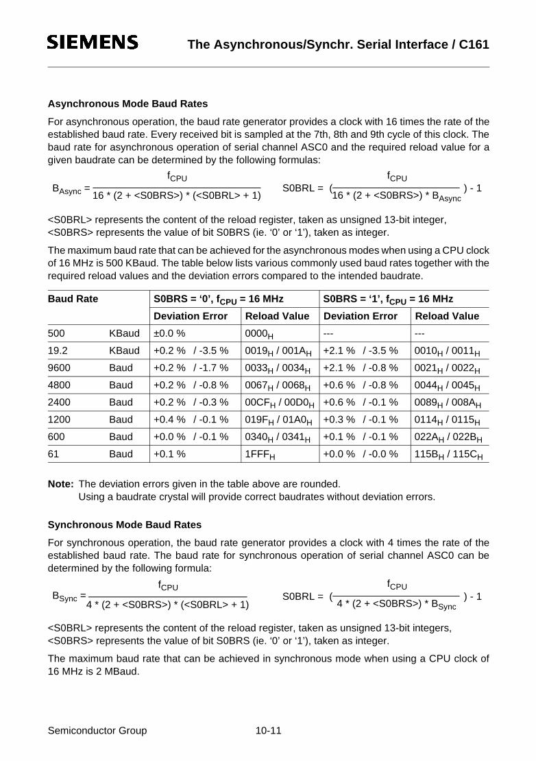
10Jul97@15:19hThe Asynchronous/Synchr. Serial Interface / C161
Asynchronous Mode Baud Rates
For asynchronous operation, the baud rate generator provides a clock with 16 times the rate of theestablished baud rate. Every received bit is sampled at the 7th, 8th and 9th cycle of this clock. Thebaud rate for asynchronous operation of serial channel ASC0 and the required reload value for agiven baudrate can be determined by the following formulas:
<S0BRL> represents the content of the reload register, taken as unsigned 13-bit integer,<S0BRS> represents the value of bit S0BRS (ie. ‘0’ or ‘1’), taken as integer.
The maximum baud rate that can be achieved for the asynchronous modes when using a CPU clockof 16 MHz is 500 KBaud. The table below lists various commonly used baud rates together with therequired reload values and the deviation errors compared to the intended baudrate.
Note: The deviation errors given in the table above are rounded.Using a baudrate crystal will provide correct baudrates without deviation errors.
Synchronous Mode Baud Rates
For synchronous operation, the baud rate generator provides a clock with 4 times the rate of theestablished baud rate. The baud rate for synchronous operation of serial channel ASC0 can bedetermined by the following formula:
<S0BRL> represents the content of the reload register, taken as unsigned 13-bit integers,<S0BRS> represents the value of bit S0BRS (ie. ‘0’ or ‘1’), taken as integer.
The maximum baud rate that can be achieved in synchronous mode when using a CPU clock of16 MHz is 2 MBaud.
Baud Rate S0BRS = ‘0’, f CPU = 16 MHz S0BRS = ‘1’, f CPU = 16 MHz
Deviation Error Reload Value Deviation Error Reload Value
500 KBaud ±0.0 % 0000H --- ---
19.2 KBaud +0.2 % / -3.5 % 0019H / 001AH +2.1 % / -3.5 % 0010H / 0011H
9600 Baud +0.2 % / -1.7 % 0033H / 0034H +2.1 % / -0.8 % 0021H / 0022H
4800 Baud +0.2 % / -0.8 % 0067H / 0068H +0.6 % / -0.8 % 0044H / 0045H
2400 Baud +0.2 % / -0.3 % 00CFH / 00D0H +0.6 % / -0.1 % 0089H / 008AH
1200 Baud +0.4 % / -0.1 % 019FH / 01A0H +0.3 % / -0.1 % 0114H / 0115H
600 Baud +0.0 % / -0.1 % 0340H / 0341H +0.1 % / -0.1 % 022AH / 022BH
61 Baud +0.1 % 1FFFH +0.0 % / -0.0 % 115BH / 115CH
BAsync =fCPU
16 * (2 + <S0BRS>) * (<S0BRL> + 1)S0BRL = (
fCPU
16 * (2 + <S0BRS>) * BAsync) - 1
BSync = S0BRL = (fCPU
4 * (2 + <S0BRS>) * BSync) - 1
fCPU
4 * (2 + <S0BRS>) * (<S0BRL> + 1)
Semiconductor Group 10-11

10Jul97@15:19hThe Asynchronous/Synchr. Serial Interface / C161
10.5 ASC0 Interrupt Control
Four bit addressable interrupt control registers are provided for serial channel ASC0. RegisterS0TIC controls the transmit interrupt, S0TBIC controls the transmit buffer interrupt, S0RIC controlsthe receive interrupt and S0EIC controls the error interrupt of serial channel ASC0. Each interruptsource also has its own dedicated interrupt vector. S0TINT is the transmit interrupt vector, S0TBINTis the transmit interrupt vector, S0RINT is the receive interrupt vector, and S0EINT is the errorinterrupt vector.
The cause of an error interrupt request (framing, parity, overrun error) can be identified by the errorstatus flags in control register S0CON.
Note: In contrary to the error interrupt request flag S0EIR, the error status flags S0FE/S0PE/S0OEare not reset automatically upon entry into the error interrupt service routine, but must becleared by software.
S0TIC (FF6CH / B6H) SFR Reset Value: - - 00H
S0RIC (FF6EH / B7H) SFR Reset Value: - - 00H
S0EIC (FF70H / B8H) SFR Reset Value: - - 00H
S0TBIC (F19CH / CEH) ESFR Reset Value: - - 00H
Note: Please refer to the general Interrupt Control Register description for an explanation of thecontrol fields.
5 4 3 2 1 011 10 9 8 7 615 14 13 12
rw rw- - - - rw rw- - - -
S0TIES0TIR GLVLILVL
5 4 3 2 1 011 10 9 8 7 615 14 13 12
rw rw- - - - rw rw- - - -
S0RIES0RIR GLVLILVL
5 4 3 2 1 011 10 9 8 7 615 14 13 12
rw rw- - - - rw rw- - - -
S0EIES0EIR GLVLILVL
S0TBIR
S0TBIE
5 4 3 2 1 011 10 9 8 7 615 14 13 12
rw rw- - - - rw rw- - - -
GLVLILVL
Semiconductor Group 10-12

10Jul97@15:19hThe Asynchronous/Synchr. Serial Interface / C161
Using the ASC0 Interrupts
For normal operation (ie. besides the error interrupt) the ASC0 provides three interrupt requests tocontrol data exchange via this serial channel:
• S0TBIR is activated when data is moved from S0TBUF to the transmit shift register.• S0TIR is activated before the last bit of an asynchronous frame is transmitted, or
after the last bit of a synchronous frame has been transmitted.• S0RIR is activated when the received frame is moved to S0RBUF.
While the task of the receive interrupt handler is quite clear, the transmitter is serviced by twointerrupt handlers. This provides advantages for the servicing software.
For single transfers is is sufficient to use the transmitter interrupt (S0TIR), which indicates that thepreviously loaded data has been transmitted, except for the last bit of an asynchronous frame.
For multiple back-to-back transfers it is necessary to load the following piece of data at last untilthe time the last bit of the previous frame has been transmitted. In asynchronous mode this leavesjust one bit-time for the handler to respond to the transmitter interrupt request, in synchronous modeit is impossible at all.Using the transmit buffer interrupt (S0TBIR) to reload transmit data gives the time to transmit acomplete frame for the service routine, as S0TBUF may be reloaded while the previous data is stillbeing transmitted.
Figure 10-6ASC0 Interrupt Generation
As shown in the figure above, S0TBIR is an early trigger for the reload routine, while S0TIRindicates the completed transmission. Software using handshake therefore should rely on S0TIR atthe end of a data block to make sure that all data has really been transmitted.
Semiconductor Group 10-13

10Jul97@15:19hThe High-Speed Synchronous Serial Interface / C161
11 The High-Speed Synchronous Serial Interface
The High-Speed Synchronous Serial Interface SSC provides flexible high-speed serialcommunication between the C161 and other microcontrollers, microprocessors or externalperipherals.
The SSC supports full-duplex and half-duplex synchronous communication up to 4 MBaud(@ 16 MHz CPU clock). The serial clock signal can be generated by the SSC itself (master mode)or be received from an external master (slave mode). Data width, shift direction, clock polarity andphase are programmable. This allows communication with SPI-compatible devices. Transmissionand reception of data is double-buffered. A 16-bit baud rate generator provides the SSC with aseparate serial clock signal.
The high-speed synchronous serial interface can be configured in a very flexible way, so it can beused with other synchronous serial interfaces (eg. the ASC0 in synchronous mode), serve formaster/slave or multimaster interconnections or operate compatible with the popular SPI interface.So it can be used to communicate with shift registers (IO expansion), peripherals (eg. EEPROMsetc.) or other controllers (networking). The SSC supports half-duplex and full-duplexcommunication. Data is transmitted or received on pins MTSR/P3.9 (Master Transmit / SlaveReceive) and MRST/P3.8 (Master Receive / Slave Transmit). The clock signal is output or input onpin SCLK/P3.13. These pins are alternate functions of Port 3 pins.
Figure 11-1SFRs and Port Pins associated with the SSC
SCLK / P3.13MTSR / P3.9MRST / P3.8
ODP3 Port 3 Open Drain Control RegisterDP3 Port 3 Direction Control RegisterSSCBR SSC Baud Rate Generator/Reload RegisterSSCTB SSC Transmit Buffer Register (write only)SSCTIC SSC Transmit Interrupt Control Register
P3 Port 3 Data RegisterSSCCON SSC Control RegisterSSCRB SSC Receive Buffer Register (read only)SSCRIC SSC Receive Interrupt Control RegisterSSCEIC SSC Error Interrupt Control Register
ODP3 E
Ports & Direction ControlAlternate Functions
Data Registers Control Registers Interrupt Control
SSCBR E SSCCON SSCTIC
DP3
P3
SSCTB E
SSCRB E
SSCRIC
SSCEIC
Semiconductor Group 11-1
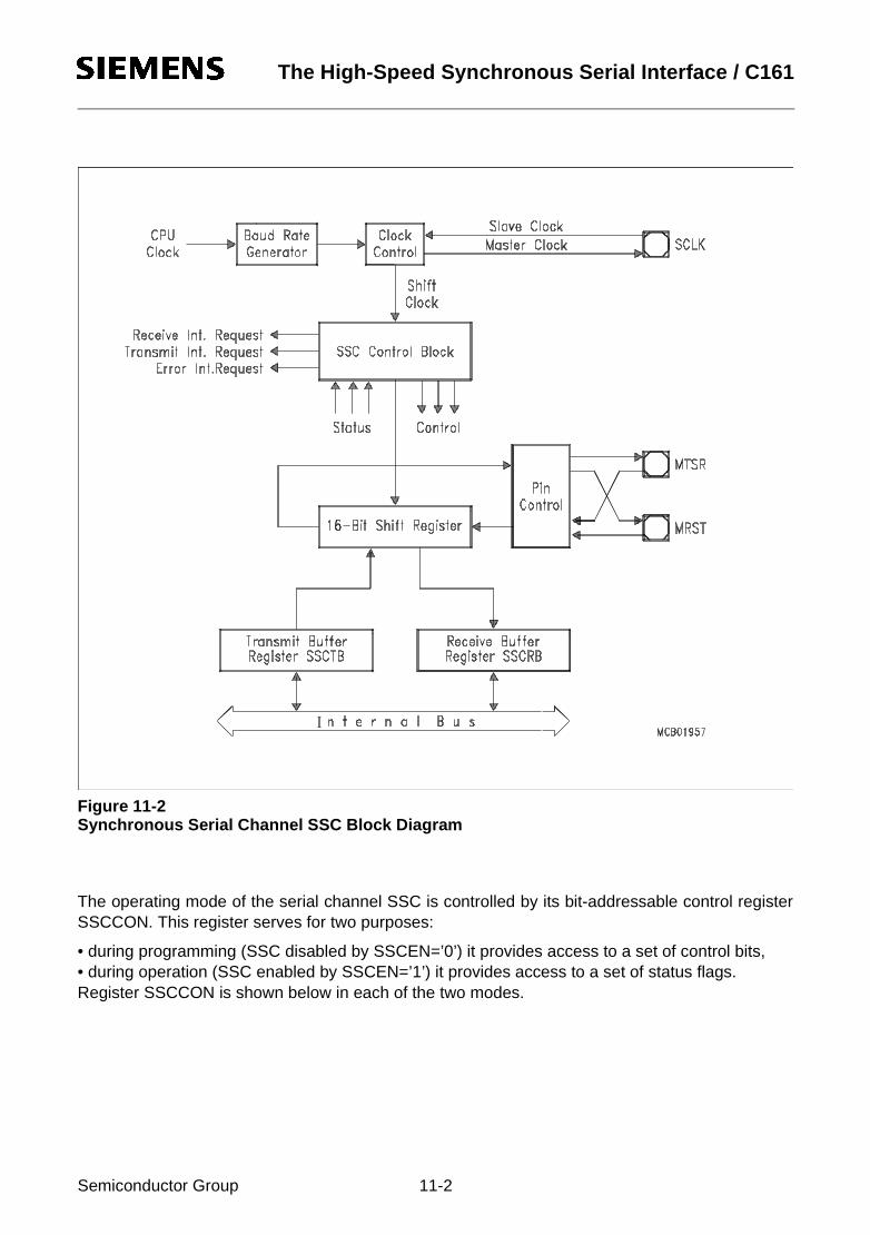
10Jul97@15:19hThe High-Speed Synchronous Serial Interface / C161
Figure 11-2Synchronous Serial Channel SSC Block Diagram
The operating mode of the serial channel SSC is controlled by its bit-addressable control registerSSCCON. This register serves for two purposes:
• during programming (SSC disabled by SSCEN=’0’) it provides access to a set of control bits,• during operation (SSC enabled by SSCEN=’1’) it provides access to a set of status flags.Register SSCCON is shown below in each of the two modes.
Semiconductor Group 11-2

10Jul97@15:19hThe High-Speed Synchronous Serial Interface / C161
SSCCON (FFB2H / D9H) SFR Reset Value: 0000H
Bit Function (Programming Mode, SSCEN = ‘0’)
SSCBM SSC Data Width Selection0 : Reserved. Do not use this combination.1...15 : Transfer Data Width is 2...16 bit (<SSCBM>+1)
SSCHB SSC Heading Control Bit0 : Transmit/Receive LSB First1 : Transmit/Receive MSB First
SSCPH SSC Clock Phase Control Bit0 : Shift transmit data on the leading clock edge, latch on trailing edge1 : Latch receive data on leading clock edge, shift on trailing edge
SSCPO SSC Clock Polarity Control Bit0 : Idle clock line is low, leading clock edge is low-to-high transition1 : Idle clock line is high, leading clock edge is high-to-low transition
SSCTEN SSC Transmit Error Enable Bit0 : Ignore transmit errors1 : Check transmit errors
SSCREN SSC Receive Error Enable Bit0 : Ignore receive errors1 : Check receive errors
SSCPEN SSC Phase Error Enable Bit0 : Ignore phase errors1 : Check phase errors
SSCBEN SSC Baudrate Error Enable Bit0 : Ignore baudrate errors1 : Check baudrate errors
SSCAREN SSC Automatic Reset Enable Bit0 : No additional action upon a baudrate error1 : The SSC is automatically reset upon a baudrate error
SSCMS SSC Master Select Bit0 : Slave Mode. Operate on shift clock received via SCLK.1 : Master Mode. Generate shift clock and output it via SCLK.
SSCEN SSC Enable Bit = ‘0’Transmission and reception disabled. Access to control bits.
5 4 3 2 1 011 10 9 8 7 615 14 13 12
rw rw rwrw rw - rwrw rw - rw
-SSCHB
SSCPH
SSCPO
rw rw
SSCBEN
SSCEN=0
SSCMS
SSCPEN
SSCREN
SSCTEN - SSCBM
SSCAREN
Semiconductor Group 11-3

10Jul97@15:19hThe High-Speed Synchronous Serial Interface / C161
SSCCON (FFB2H / D9H) SFR Reset Value: 0000H
Note: • The target of an access to SSCCON (control bits or flags) is determined by the state ofSSCEN prior to the access, ie. writing C057H to SSCCON in programming mode(SSCEN=’0’) will initialize the SSC (SSCEN was ‘0’) and then turn it on (SSCEN=’1’).• When writing to SSCCON, make sure that reserved locations receive zeros.
The shift register of the SSC is connected to both the transmit pin and the receive pin via the pincontrol logic (see block diagram). Transmission and reception of serial data is synchronized andtakes place at the same time, ie. the same number of transmitted bits is also received. Transmit datais written into the Transmit Buffer SSCTB. It is moved to the shift register as soon as this is empty.An SSC-master (SSCMS=’1’) immediately begins transmitting, while an SSC-slave (SSCMS=’0’)will wait for an active shift clock. When the transfer starts, the busy flag SSCBSY is set and atransmit interrupt request (SSCTIR) will be generated to indicate that SSCTB may be reloadedagain. When the programmed number of bits (2...16) has been transferred, the contents of the shiftregister are moved to the Receive Buffer SSCRB and a receive interrupt request (SSCRIR) will begenerated. If no further transfer is to take place (SSCTB is empty), SSCBSY will be cleared at thesame time. Software should not modify SSCBSY, as this flag is hardware controlled.
Note: Only one SSC (etc.) can be master at a given time.
Bit Function (Operating Mode, SSCEN = ‘1’)
SSCBC SSC Bit Count FieldShift counter is updated with every shifted bit. Do not write to!!!
SSCTE SSC Transmit Error Flag1 : Transfer starts with the slave’s transmit buffer not being updated
SSCRE SSC Receive Error Flag1 : Reception completed before the receive buffer was read
SSCPE SSC Phase Error Flag1 : Received data changes around sampling clock edge
SSCBE SSC Baudrate Error Flag1 : More than factor 2 or 0.5 between Slave’s actual and expected
baudrate
SSCBSY SSC Busy FlagSet while a transfer is in progress. Do not write to!!!
SSCMS SSC Master Select Bit0 : Slave Mode. Operate on shift clock received via SCLK.1 : Master Mode. Generate shift clock and output it via SCLK.
SSCEN SSC Enable Bit = ‘1’Transmission and reception enabled. Access to status flags and M/S control.
5 4 3 2 1 011 10 9 8 7 615 14 13 12
- - rrw rw - -rw rw - rw
-
rw rw
SSCBE
SSCEN=1
SSCMS
SSCPE
SSCRE
SSCTE -
SSCBSY - - - SSCBC
Semiconductor Group 11-4

10Jul97@15:19hThe High-Speed Synchronous Serial Interface / C161
The transfer of serial data bits can be programmed in many respects:
• the data width can be chosen from 2 bits to 16 bits• transfer may start with the LSB or the MSB• the shift clock may be idle low or idle high• data bits may be shifted with the leading or trailing edge of the clock signal• the baudrate may be set from 122 Bd up to 4 MBd (@ 16 MHz CPU clock)• the shift clock can be generated (master) or received (slave)
This allows the adaptation of the SSC to a wide range of applications, where serial data transfer isrequired.
The Data Width Selection supports the transfer of frames of any length, from 2-bit “characters” upto 16-bit “characters”. Starting with the LSB (SSCHB=’0’) allows communication eg. with ASC0devices in synchronous mode (C166 family) or 8051 like serial interfaces. Starting with the MSB(SSCHB=’1’) allows operation compatible with the SPI interface.Regardless which data width is selected and whether the MSB or the LSB is transmitted first, thetransfer data is always right aligned in registers SSCTB and SSCRB, with the LSB of the transferdata in bit 0 of these registers. The data bits are rearranged for transfer by the internal shift registerlogic. The unselected bits of SSCTB are ignored, the unselected bits of SSCRB will be not valid andshould be ignored by the receiver service routine.
The Clock Control allows the adaptation of transmit and receive behaviour of the SSC to a varietyof serial interfaces. A specific clock edge (rising or falling) is used to shift out transmit data, while theother clock edge is used to latch in receive data. Bit SSCPH selects the leading edge or the trailingedge for each function. Bit SSCPO selects the level of the clock line in the idle state. So for an idle-high clock the leading edge is a falling one, a 1-to-0 transition. The figure below is a summary.
Figure 11-3Serial Clock Phase and Polarity Options
Semiconductor Group 11-5
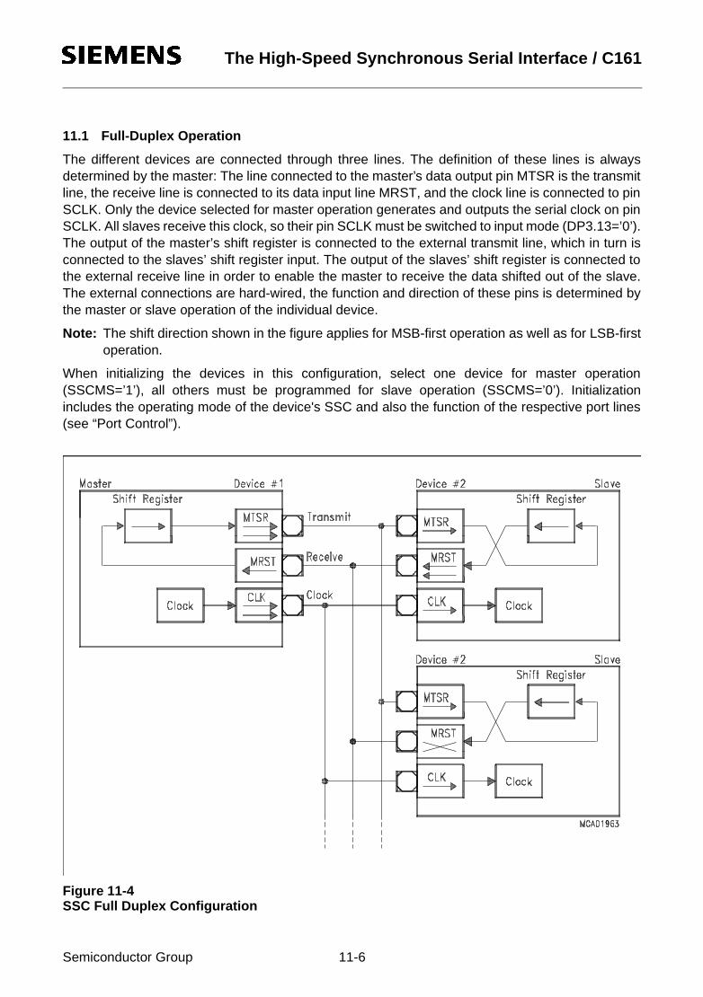
10Jul97@15:19hThe High-Speed Synchronous Serial Interface / C161
11.1 Full-Duplex Operation
The different devices are connected through three lines. The definition of these lines is alwaysdetermined by the master: The line connected to the master’s data output pin MTSR is the transmitline, the receive line is connected to its data input line MRST, and the clock line is connected to pinSCLK. Only the device selected for master operation generates and outputs the serial clock on pinSCLK. All slaves receive this clock, so their pin SCLK must be switched to input mode (DP3.13=’0’).The output of the master’s shift register is connected to the external transmit line, which in turn isconnected to the slaves’ shift register input. The output of the slaves’ shift register is connected tothe external receive line in order to enable the master to receive the data shifted out of the slave.The external connections are hard-wired, the function and direction of these pins is determined bythe master or slave operation of the individual device.
Note: The shift direction shown in the figure applies for MSB-first operation as well as for LSB-firstoperation.
When initializing the devices in this configuration, select one device for master operation(SSCMS=’1’), all others must be programmed for slave operation (SSCMS=’0’). Initializationincludes the operating mode of the device's SSC and also the function of the respective port lines(see “Port Control”).
Figure 11-4SSC Full Duplex Configuration
Semiconductor Group 11-6
10Jul97@15:19hThe High-Speed Synchronous Serial Interface / C161
The data output pins MRST of all slave devices are connected together onto the one receive line inthis configuration. During a transfer each slave shifts out data from its shift register. There are twoways to avoid collisions on the receive line due to different slave data:
Only one slave drives the line, ie. enables the driver of its MRST pin. All the other slaves have toprogram there MRST pins to input. So only one slave can put its data onto the master’s receive line.Only receiving of data from the master is possible. The master selects the slave device from whichit expects data either by separate select lines, or by sending a special command to this slave. Theselected slave then switches its MRST line to output, until it gets a deselection signal or command.
The slaves use open drain output on MRST. This forms a Wired-AND connection. The receiveline needs an external pullup in this case. Corruption of the data on the receive line sent by theselected slave is avoided, when all slaves which are not selected for transmission to the master onlysend ones (‘1’). Since this high level is not actively driven onto the line, but only held through thepullup device, the selected slave can pull this line actively to a low level when transmitting a zero bit.The master selects the slave device from which it expects data either by separate select lines, or bysending a special command to this slave.
After performing all necessary initializations of the SSC, the serial interfaces can be enabled. For amaster device, the alternate clock line will now go to its programmed polarity. The alternate data linewill go to either '0' or '1', until the first transfer will start. After a transfer the alternate data line willalways remain at the logic level of the last transmitted data bit.
When the serial interfaces are enabled, the master device can initiate the first data transfer bywriting the transmit data into register SSCTB. This value is copied into the shift register (which isassumed to be empty at this time), and the selected first bit of the transmit data will be placed ontothe MTSR line on the next clock from the baudrate generator (transmission only starts, ifSSCEN=’1’). Depending on the selected clock phase, also a clock pulse will be generated on theSCLK line. With the opposite clock edge the master at the same time latches and shifts in the datadetected at its input line MRST. This “exchanges” the transmit data with the receive data. Since theclock line is connected to all slaves, their shift registers will be shifted synchronously with themaster's shift register, shifting out the data contained in the registers, and shifting in the datadetected at the input line. After the preprogrammed number of clock pulses (via the data widthselection) the data transmitted by the master is contained in all slaves’ shift registers, while themaster's shift register holds the data of the selected slave. In the master and all slaves the contentof the shift register is copied into the receive buffer SSCRB and the receive interrupt flag SSCRIRis set.
A slave device will immediately output the selected first bit (MSB or LSB of the transfer data) at pinMRST, when the content of the transmit buffer is copied into the slave's shift register. It will not waitfor the next clock from the baudrate generator, as the master does. The reason for this is that,depending on the selected clock phase, the first clock edge generated by the master may bealready used to clock in the first data bit. So the slave's first data bit must already be valid at thistime.
Semiconductor Group 11-7

10Jul97@15:19hThe High-Speed Synchronous Serial Interface / C161
Note: On the SSC always a transmission and a reception takes place at the same time, regardlesswhether valid data has been transmitted or received. This is different eg. from asynchronousreception on ASC0.
The initialization of the SCLK pin on the master requires some attention in order to avoidundesired clock transitions, which may disturb the other receivers. The state of the internal alternateoutput lines is ’1’ as long as the SSC is disabled. This alternate output signal is ANDed with therespective port line output latch. Enabling the SSC with an idle-low clock (SSCPO=’0’) will drive thealternate data output and (via the AND) the port pin SCLK immediately low. To avoid this, use thefollowing sequence:
• select the clock idle level (SSCPO=’x’)• load the port output latch with the desired clock idle level (P3.13=’x’)• switch the pin to output (DP3.13=’1’)• enable the SSC (SSCEN=’1’)• if SSCPO=’0’: enable alternate data output (P3.13=’1’)
The same mechanism as for selecting a slave for transmission (separate select lines or specialcommands) may also be used to move the role of the master to another device in the network. Inthis case the previous master and the future master (previous slave) will have to toggle theiroperating mode (SSCMS) and the direction of their port pins (see description above).
11.2 Half Duplex Operation
In a half duplex configuration only one data line is necessary for both receiving and transmitting ofdata. The data exchange line is connected to both pins MTSR and MRST of each device, the clockline is connected to the SCLK pin.
The master device controls the data transfer by generating the shift clock, while the slave devicesreceive it. Due to the fact that all transmit and receive pins are connected to the one data exchangeline, serial data may be moved between arbitrary stations.
Similar to full duplex mode there are two ways to avoid collisions on the data exchange line:
• only the transmitting device may enable its transmit pin driver
• the non-transmitting devices use open drain output and only send ones.
Since the data inputs and outputs are connected together, a transmitting device will clock in its owndata at the input pin (MRST for a master device, MTSR for a slave). By these means any corruptionson the common data exchange line are detected, where the received data is not equal to thetransmitted data.
Semiconductor Group 11-8

10Jul97@15:19hThe High-Speed Synchronous Serial Interface / C161
Figure 11-5SSC Half Duplex Configuration
Continuous Transfers
When the transmit interrupt request flag is set, it indicates that the transmit buffer SSCTB is emptyand ready to be loaded with the next transmit data. If SSCTB has been reloaded by the time thecurrent transmission is finished, the data is immediately transferred to the shift register and the nexttransmission will start without any additional delay. On the data line there is no gap between the twosuccessive frames. Eg. two byte transfers would look the same as one word transfer. This featurecan be used to interface with devices which can operate with or require more than 16 data bits pertransfer. It is just a matter of software, how long a total data frame length can be. This option canalso be used eg. to interface to byte-wide and word-wide devices on the same serial bus.
Note: Of course, this can only happen in multiples of the selected basic data width, since it wouldrequire disabling/enabling of the SSC to reprogram the basic data width on-the-fly.
Semiconductor Group 11-9
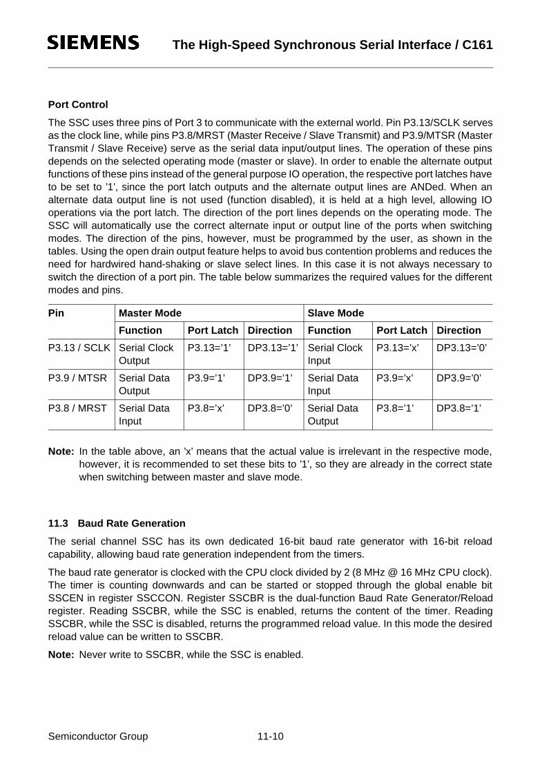
10Jul97@15:19hThe High-Speed Synchronous Serial Interface / C161
Port Control
The SSC uses three pins of Port 3 to communicate with the external world. Pin P3.13/SCLK servesas the clock line, while pins P3.8/MRST (Master Receive / Slave Transmit) and P3.9/MTSR (MasterTransmit / Slave Receive) serve as the serial data input/output lines. The operation of these pinsdepends on the selected operating mode (master or slave). In order to enable the alternate outputfunctions of these pins instead of the general purpose IO operation, the respective port latches haveto be set to ’1’, since the port latch outputs and the alternate output lines are ANDed. When analternate data output line is not used (function disabled), it is held at a high level, allowing IOoperations via the port latch. The direction of the port lines depends on the operating mode. TheSSC will automatically use the correct alternate input or output line of the ports when switchingmodes. The direction of the pins, however, must be programmed by the user, as shown in thetables. Using the open drain output feature helps to avoid bus contention problems and reduces theneed for hardwired hand-shaking or slave select lines. In this case it is not always necessary toswitch the direction of a port pin. The table below summarizes the required values for the differentmodes and pins.
Note: In the table above, an ’x’ means that the actual value is irrelevant in the respective mode,however, it is recommended to set these bits to ’1’, so they are already in the correct statewhen switching between master and slave mode.
11.3 Baud Rate Generation
The serial channel SSC has its own dedicated 16-bit baud rate generator with 16-bit reloadcapability, allowing baud rate generation independent from the timers.
The baud rate generator is clocked with the CPU clock divided by 2 (8 MHz @ 16 MHz CPU clock).The timer is counting downwards and can be started or stopped through the global enable bitSSCEN in register SSCCON. Register SSCBR is the dual-function Baud Rate Generator/Reloadregister. Reading SSCBR, while the SSC is enabled, returns the content of the timer. ReadingSSCBR, while the SSC is disabled, returns the programmed reload value. In this mode the desiredreload value can be written to SSCBR.
Note: Never write to SSCBR, while the SSC is enabled.
Pin Master Mode Slave Mode
Function Port Latch Direction Function Port Latch Direction
P3.13 / SCLK Serial Clock Output
P3.13=’1’ DP3.13=’1’ Serial Clock Input
P3.13=’x’ DP3.13=’0’
P3.9 / MTSR Serial Data Output
P3.9=’1’ DP3.9=’1’ Serial Data Input
P3.9=’x’ DP3.9=’0’
P3.8 / MRST Serial Data Input
P3.8=’x’ DP3.8=’0’ Serial Data Output
P3.8=’1’ DP3.8=’1’
Semiconductor Group 11-10

10Jul97@15:19hThe High-Speed Synchronous Serial Interface / C161
The formulas below calculate either the resulting baud rate for a given reload value, or the requiredreload value for a given baudrate:
<SSCBR> represents the content of the reload register, taken as unsigned 16-bit integer.
The maximum baud rate that can be achieved when using a CPU clock of 16 MHz is 4 MBaud. Thetable below lists some possible baud rates together with the required reload values and the resultingbit times, assuming a CPU clock of 16 MHz.
Note: The content of SSCBR must be > 0.
Baud Rate Bit Time Reload Value
Reserved. Use a reload value > 0. --- --- 0000H
4 MBaud 250 ns 0001H
2.67 MBaud 375 ns 0002H
2 MBaud 500 ns 0003H
1.6 MBaud 625 ns 0004H
1.0 MBaud 1 µs 0007H
100 KBaud 10 µs 004FH
10 KBaud 100 µs 031FH
1.0 KBaud 1 ms 1F3FH
122.1 Baud 8.2 ms FFFFH
BSSC =fCPU
2 * (<SSCBR> + 1)SSCBR = (
fCPU
2 * BaudrateSSC) - 1
Semiconductor Group 11-11

10Jul97@15:19hThe High-Speed Synchronous Serial Interface / C161
11.4 Error Detection Mechanisms
The SSC is able to detect four different error conditions. Receive Error and Phase Error aredetected in all modes, while Transmit Error and Baudrate Error only apply to slave mode. When anerror is detected, the respective error flag is set. When the corresponding Error Enable Bit is set,also an error interrupt request will be generated by setting SSCEIR (see figure below). The errorinterrupt handler may then check the error flags to determine the cause of the error interrupt. Theerror flags are not reset automatically (like SSCEIR), but rather must be cleared by software afterservicing. This allows servicing of some error conditions via interrupt, while the others may be polledby software.
Note: The error interrupt handler must clear the associated (enabled) errorflag(s) to preventrepeated interrupt requests.
A Receive Error (Master or Slave mode) is detected, when a new data frame is completelyreceived, but the previous data was not read out of the receive buffer register SSCRB. Thiscondition sets the error flag SSCRE and, when enabled via SSCREN, the error interrupt requestflag SSCEIR. The old data in the receive buffer SSCRB will be overwritten with the new value andis unretrievably lost.
A Phase Error (Master or Slave mode) is detected, when the incoming data at pin MRST (mastermode) or MTSR (slave mode), sampled with the same frequency as the CPU clock, changesbetween one sample before and two samples after the latching edge of the clock signal (see “ClockControl”). This condition sets the error flag SSCPE and, when enabled via SSCPEN, the errorinterrupt request flag SSCEIR.
A Baud Rate Error (Slave mode) is detected, when the incoming clock signal deviates from theprogrammed baud rate by more than 100%, ie. it either is more than double or less than half theexpected baud rate. This condition sets the error flag SSCBE and, when enabled via SSCBEN, theerror interrupt request flag SSCEIR. Using this error detection capability requires that the slave'sbaud rate generator is programmed to the same baud rate as the master device. This featuredetects false additional, or missing pulses on the clock line (within a certain frame).
Note: If this error condition occurs and bit SSCAREN=’1’, an automatic reset of the SSC will beperformed in case of this error. This is done to reinitialize the SSC, if too few or too manyclock pulses have been detected.
Semiconductor Group 11-12
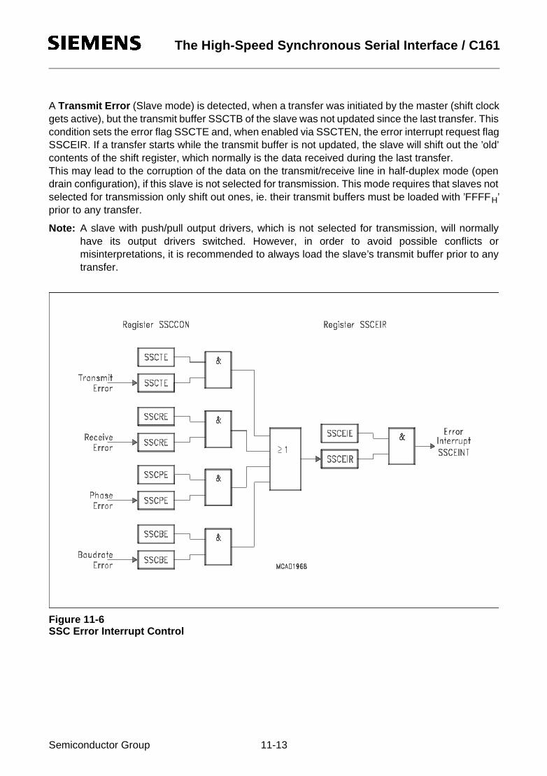
10Jul97@15:19hThe High-Speed Synchronous Serial Interface / C161
A Transmit Error (Slave mode) is detected, when a transfer was initiated by the master (shift clockgets active), but the transmit buffer SSCTB of the slave was not updated since the last transfer. Thiscondition sets the error flag SSCTE and, when enabled via SSCTEN, the error interrupt request flagSSCEIR. If a transfer starts while the transmit buffer is not updated, the slave will shift out the ’old’contents of the shift register, which normally is the data received during the last transfer.This may lead to the corruption of the data on the transmit/receive line in half-duplex mode (opendrain configuration), if this slave is not selected for transmission. This mode requires that slaves notselected for transmission only shift out ones, ie. their transmit buffers must be loaded with ’FFFFH’prior to any transfer.
Note: A slave with push/pull output drivers, which is not selected for transmission, will normallyhave its output drivers switched. However, in order to avoid possible conflicts ormisinterpretations, it is recommended to always load the slave’s transmit buffer prior to anytransfer.
Figure 11-6SSC Error Interrupt Control
Semiconductor Group 11-13

10Jul97@15:19hThe High-Speed Synchronous Serial Interface / C161
11.5 SSC Interrupt Control
Three bit addressable interrupt control registers are provided for serial channel SSC. RegisterSSCTIC controls the transmit interrupt, SSCRIC controls the receive interrupt and SSCEIC controlsthe error interrupt of serial channel SSC. Each interrupt source also has its own dedicated interruptvector. SCTINT is the transmit interrupt vector, SCRINT is the receive interrupt vector, and SCEINTis the error interrupt vector.
The cause of an error interrupt request (receive, phase, baudrate, transmit error) can be identifiedby the error status flags in control register SSCCON.
Note: In contrary to the error interrupt request flag SSCEIR, the error status flags SSCxE are notreset automatically upon entry into the error interrupt service routine, but must be cleared bysoftware.
SSCTIC (FF72H / B9H) SFR Reset Value: - - 00H
SSCRIC (FF74H / BAH) SFR Reset Value: - - 00H
SSCEIC (FF76H / BBH) SFR Reset Value: - - 00H
Note: Please refer to the general Interrupt Control Register description for an explanation of thecontrol fields.
SSCTIE
SSCTIR
5 4 3 2 1 011 10 9 8 7 615 14 13 12
rw rw- - - - rw rw- - - -
GLVLILVL
SSCRIE
SSCRIR
5 4 3 2 1 011 10 9 8 7 615 14 13 12
rw rw- - - - rw rw- - - -
GLVLILVL
SSCEIR
SSCEIE
5 4 3 2 1 011 10 9 8 7 615 14 13 12
rw rw- - - - rw rw- - - -
GLVLILVL
Semiconductor Group 11-14
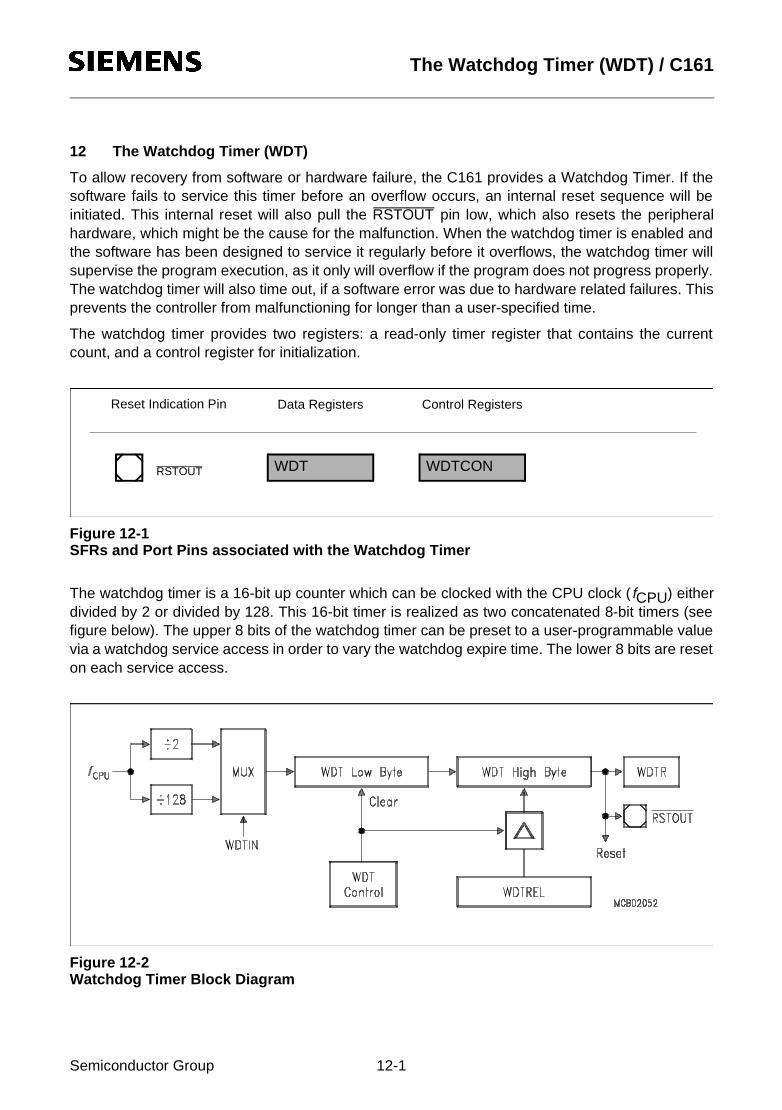
10Jul97@15:19h The Watchdog Timer (WDT) / C161
12 The Watchdog Timer (WDT)
To allow recovery from software or hardware failure, the C161 provides a Watchdog Timer. If thesoftware fails to service this timer before an overflow occurs, an internal reset sequence will beinitiated. This internal reset will also pull the RSTOUT pin low, which also resets the peripheralhardware, which might be the cause for the malfunction. When the watchdog timer is enabled andthe software has been designed to service it regularly before it overflows, the watchdog timer willsupervise the program execution, as it only will overflow if the program does not progress properly.The watchdog timer will also time out, if a software error was due to hardware related failures. Thisprevents the controller from malfunctioning for longer than a user-specified time.
The watchdog timer provides two registers: a read-only timer register that contains the currentcount, and a control register for initialization.
Figure 12-1SFRs and Port Pins associated with the Watchdog Timer
The watchdog timer is a 16-bit up counter which can be clocked with the CPU clock (fCPU) eitherdivided by 2 or divided by 128. This 16-bit timer is realized as two concatenated 8-bit timers (seefigure below). The upper 8 bits of the watchdog timer can be preset to a user-programmable valuevia a watchdog service access in order to vary the watchdog expire time. The lower 8 bits are reseton each service access.
Figure 12-2Watchdog Timer Block Diagram
WDTCONRSTOUT
Reset Indication Pin Data Registers Control Registers
WDT
Semiconductor Group 12-1
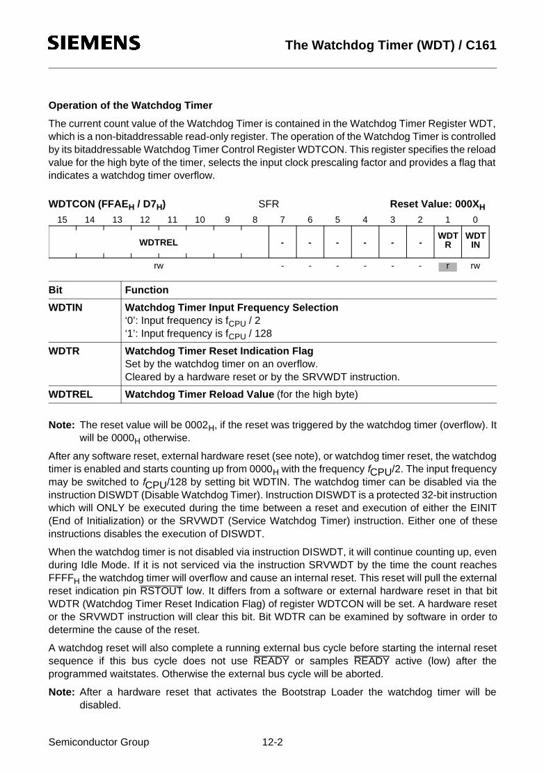
10Jul97@15:19h The Watchdog Timer (WDT) / C161
Operation of the Watchdog Timer
The current count value of the Watchdog Timer is contained in the Watchdog Timer Register WDT,which is a non-bitaddressable read-only register. The operation of the Watchdog Timer is controlledby its bitaddressable Watchdog Timer Control Register WDTCON. This register specifies the reloadvalue for the high byte of the timer, selects the input clock prescaling factor and provides a flag thatindicates a watchdog timer overflow.
WDTCON (FFAEH / D7H) SFR Reset Value: 000XH
Note: The reset value will be 0002H, if the reset was triggered by the watchdog timer (overflow). Itwill be 0000H otherwise.
After any software reset, external hardware reset (see note), or watchdog timer reset, the watchdogtimer is enabled and starts counting up from 0000H with the frequency fCPU/2. The input frequencymay be switched to fCPU/128 by setting bit WDTIN. The watchdog timer can be disabled via theinstruction DISWDT (Disable Watchdog Timer). Instruction DISWDT is a protected 32-bit instructionwhich will ONLY be executed during the time between a reset and execution of either the EINIT(End of Initialization) or the SRVWDT (Service Watchdog Timer) instruction. Either one of theseinstructions disables the execution of DISWDT.
When the watchdog timer is not disabled via instruction DISWDT, it will continue counting up, evenduring Idle Mode. If it is not serviced via the instruction SRVWDT by the time the count reachesFFFFH the watchdog timer will overflow and cause an internal reset. This reset will pull the externalreset indication pin RSTOUT low. It differs from a software or external hardware reset in that bitWDTR (Watchdog Timer Reset Indication Flag) of register WDTCON will be set. A hardware resetor the SRVWDT instruction will clear this bit. Bit WDTR can be examined by software in order todetermine the cause of the reset.
A watchdog reset will also complete a running external bus cycle before starting the internal resetsequence if this bus cycle does not use READY or samples READY active (low) after theprogrammed waitstates. Otherwise the external bus cycle will be aborted.
Note: After a hardware reset that activates the Bootstrap Loader the watchdog timer will bedisabled.
Bit Function
WDTIN Watchdog Timer Input Frequency Selection‘0’: Input frequency is fCPU / 2‘1’: Input frequency is fCPU / 128
WDTR Watchdog Timer Reset Indication FlagSet by the watchdog timer on an overflow.Cleared by a hardware reset or by the SRVWDT instruction.
WDTREL Watchdog Timer Reload Value (for the high byte)
-WDT
R-WDT
IN- ---
5 4 3 2 1 011 10 9 8 7 615 14 13 12
- - - rrw - -
WDTREL
- rw
Semiconductor Group 12-2
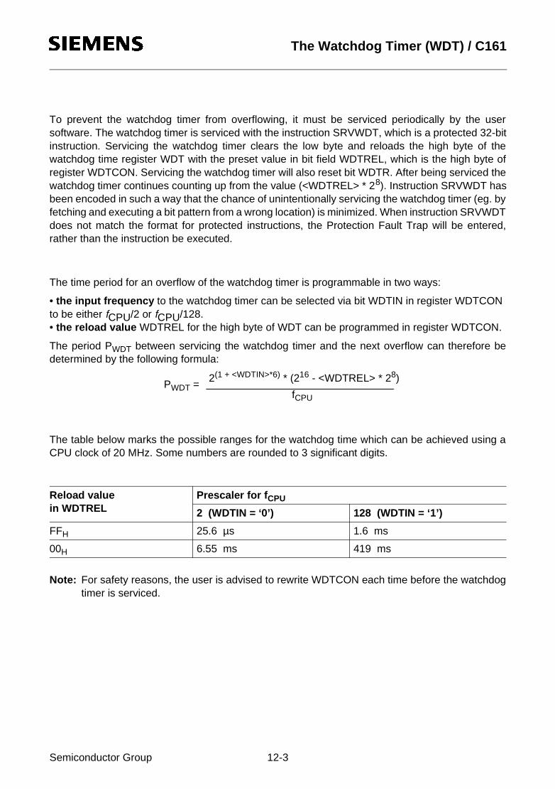
10Jul97@15:19h The Watchdog Timer (WDT) / C161
To prevent the watchdog timer from overflowing, it must be serviced periodically by the usersoftware. The watchdog timer is serviced with the instruction SRVWDT, which is a protected 32-bitinstruction. Servicing the watchdog timer clears the low byte and reloads the high byte of thewatchdog time register WDT with the preset value in bit field WDTREL, which is the high byte ofregister WDTCON. Servicing the watchdog timer will also reset bit WDTR. After being serviced thewatchdog timer continues counting up from the value (<WDTREL> * 28). Instruction SRVWDT hasbeen encoded in such a way that the chance of unintentionally servicing the watchdog timer (eg. byfetching and executing a bit pattern from a wrong location) is minimized. When instruction SRVWDTdoes not match the format for protected instructions, the Protection Fault Trap will be entered,rather than the instruction be executed.
The time period for an overflow of the watchdog timer is programmable in two ways:
• the input frequency to the watchdog timer can be selected via bit WDTIN in register WDTCONto be either fCPU/2 or fCPU/128.• the reload value WDTREL for the high byte of WDT can be programmed in register WDTCON.
The period PWDT between servicing the watchdog timer and the next overflow can therefore bedetermined by the following formula:
The table below marks the possible ranges for the watchdog time which can be achieved using aCPU clock of 20 MHz. Some numbers are rounded to 3 significant digits.
Note: For safety reasons, the user is advised to rewrite WDTCON each time before the watchdogtimer is serviced.
Reload valuein WDTREL
Prescaler for fCPU
2 (WDTIN = ‘0’) 128 (WDTIN = ‘1’)
FFH 25.6 µs 1.6 ms
00H 6.55 ms 419 ms
PWDT =fCPU
2(1 + <WDTIN>*6) * (216 - <WDTREL> * 28)
Semiconductor Group 12-3

10Jul97@15:19h The Bootstrap Loader / C161
13 The Bootstrap Loader
The built-in bootstrap loader of the C161 provides a mechanism to load the startup program, whichis executed after reset, via the serial interface. In this case no external (ROM) memory or an internalROM is required for the initialization code starting at location 00’0000H.
Note: The built-in bootstrap loader is not available in the C161V.
The bootstrap loader moves code/data into the internal RAM, but it is also possible to transfer datavia the serial interface into an external RAM using a second level loader routine. ROM memory(internal or external) is not necessary. However, it may be used to provide lookup tables or mayprovide “core-code”, ie. a set of general purpose subroutines, eg. for IO operations, numbercrunching, system initialization, etc.
Figure 13-1Bootstrap Loader Sequence
The Bootstrap Loader may be used to load the complete application software into ROMlesssystems, it may load temporary software into complete systems for testing or calibration, it may alsobe used to load a programming routine for Flash devices.
The BSL mechanism may be used for standard system startup as well as only for special occasionslike system maintenance (firmware update) or end-of-line programming or testing.
1) BSL initialization time, > 2 µs @ fCPU = 20 MHz.2) Zero byte (1 start bit, eight ‘0’ data bits, 1 stop bit), sent by host.3) Identification byte, sent by C161.4) 32 bytes of code / data, sent by host.5) Caution: TxD0 is only driven a certain time after reception of the zero byte (2.5 µs @ fCPU = 20 MHz).6) Internal Boot ROM.
Semiconductor Group 13-1

10Jul97@15:19h The Bootstrap Loader / C161
Entering the Bootstrap Loader
The C161 enters BSL mode, if pin P0L.4 is sampled low at the end of a hardware reset. In this casethe built-in bootstrap loader is activated independent of the selected bus mode. The bootstraploader code is stored in a special Boot-ROM, no part of the standard mask ROM or Flash memoryarea is required for this.
After entering BSL mode and the respective initialization the C161 scans the RXD0 line to receivea zero byte, ie. one start bit, eight ‘0’ data bits and one stop bit. From the duration of this zero byteit calculates the corresponding baudrate factor with respect to the current CPU clock, initializes theserial interface ASC0 accordingly and switches pin TxD0 to output. Using this baudrate, anidentification byte is returned to the host that provides the loaded data.This identification byte identifies the device to be bootet. The following codes are defined:8xC166: 55HC165: B5HC167: C5H (previous versions returned A5H).
When the C161 has entered BSL mode, the following configuration is automatically set (values thatdeviate from the normal reset values, are marked):
Watchdog Timer: Disabled Register SYSCON: 0E00H Context Pointer CP: FA00H Register STKUN: FA40H Stack Pointer SP: FA40H Register STKOV: FA0CH 0<->CRegister S0CON: 8011H Register BUSCON0: acc. to startup config.Register S0BG: acc. to ‘00’ byte P3.10 / TXD0: ‘1’
DP3.10: ‘1’
Other than after a normal reset the watchdog timer is disabled, so the bootstrap loading sequenceis not time limited. Pin TXD0 is configured as output, so the C161 can return the identification byte.
Note: Even if the internal ROM is enabled, no code can be executed out of it.
The hardware that activates the BSL during reset may be a simple pull-down resistor on P0L.4 forsystems that use this feature upon every hardware reset. You may want to use a switchable solution(via jumper or an external signal) for systems that only temporarily use the bootstrap loader.
Figure 13-2Hardware Provisions to Activate the BSL
Semiconductor Group 13-2
10Jul97@15:19h The Bootstrap Loader / C161
After sending the identification byte the ASC0 receiver is enabled and is ready to receive the initial32 bytes from the host. A half duplex connection is therefore sufficient to feed the BSL.
Memory Configuration after Reset
The configuration (ie. the accessibility) of the C161’s memory areas after reset in Bootstrap-Loadermode differs from the standard case. Pin EA is not evaluated when BSL mode is selected, andaccesses to the internal ROM area are partly redirected, while the C161 is in BSL mode (see tablebelow). All code fetches are made from the special Boot-ROM, while data accesses read from theinternal user ROM. Data accesses will return undefined values on ROMless devices.
Note: The code in the Boot-ROM is not an invariant feature of the C161. User software should nottry to execute code from the internal ROM area while the BSL mode is still active, as thesefetches will be redirected to the Boot-ROM.The Boot-ROM will also “move” to segment 1, when the internal ROM area is mapped tosegment 1.
16 MBytes 16 MBytes 16 MBytes
BSL mode active Yes (P0L.4=’0’) Yes (P0L.4=’0’) No (P0L.4=’1’)
EA pin high low acc. to application
Code fetch from internal ROM area
Boot-ROM access Boot-ROM access User ROM access
Data fetch from internal ROM area
User ROM access User ROM access User ROM access
int. ROMenabled
Boo
t-R
OM
user
RO
M
access to
externalbusdisabled
access to
int.RAM
1
0
255
int. ROMenabled
Boo
t-R
OM
user
RO
M
access to
externalbusenabled
access to
int.RAM
1
0
255
Depends on reset config.
user
RO
M int.RAM
255
1
0
Depends on reset config.(EA, P0)
Semiconductor Group 13-3

10Jul97@15:19h The Bootstrap Loader / C161
Loading the Startup Code
After sending the identification byte the BSL enters a loop to receive 32 bytes via ASC0. Thesebytes are stored sequentially into locations 00’FA40H through 00’FA5FH of the internal RAM. So upto 16 instructions may be placed into the RAM area. To execute the loaded code the BSL thenjumps to location 00’FA40H, ie. the first loaded instruction. The bootstrap loading sequence is nowterminated, the C161 remains in BSL mode, however. Most probably the initially loaded routine willload additional code or data, as an average application is likely to require substantially more than 16instructions. This second receive loop may directly use the pre-initialized interface ASC0 to receivedata and store it to arbitrary user-defined locations.
This second level of loaded code may be the final application code. It may also be another, moresophisticated, loader routine that adds a transmission protocol to enhance the integrity of the loadedcode or data. It may also contain a code sequence to change the system configuration and enablethe bus interface to store the received data into external memory.
This process may go through several iterations or may directly execute the final application. In allcases the C161 will still run in BSL mode, ie. with the watchdog timer disabled and limited accessto the internal ROM area. All code fetches from the internal ROM area (00’0000H...00’7FFFH or01’0000H...01’7FFFH, if mapped to segment 1) are redirected to the special Boot-ROM. Datafetches access will access the internal ROM of the C161, if any is available, but will return undefineddata on ROMless devices.
Exiting Bootstrap Loader Mode
In order to execute a program in normal mode, the BSL mode must be terminated first. The C161exits BSL mode upon a software reset (ignores the level on P0L.4) or a hardware reset (P0L.4 mustbe high then!). After a reset the C161 will start executing from location 00’0000H of the internal ROMor the external memory, as programmed via pin EA.
Choosing the Baudrate for the BSL
The calculation of the serial baudrate for ASC0 from the length of the first zero byte that is received,allows the operation of the bootstrap loader of the C161 with a wide range of baudrates. However,the upper and lower limits have to be kept, in order to insure proper data transfer.
The C161 uses timer T6 to measure the length of the initial zero byte. The quantization uncertaintyof this measurement implies the first deviation from the real baudrate, the next deviation is impliedby the computation of the S0BRL reload value from the timer contents. The formula below showsthe association:
fCPU32 S0BRL 1+( )⋅-------------------------------------------BC161 =
S0BRLT6 36–
72-------------------= T694--
fCPUBHost---------------⋅=,
Semiconductor Group 13-4

10Jul97@15:19h The Bootstrap Loader / C161
For a correct data transfer from the host to the C161 the maximum deviation between the internalinitialized baudrate for ASC0 and the real baudrate of the host should be below 2.5%. The deviation(FB, in percent) between host baudrate and C161 baudrate can be calculated via the formula below:
Note: Function (FB) does not consider the tolerances of oscillators and other devices supportingthe serial communication.
This baudrate deviation is a nonlinear function depending on the CPU clock and the baudrate of thehost. The maxima of the function (FB) increase with the host baudrate due to the smaller baudrateprescaler factors and the implied higher quantization error (see figure below).
Figure 13-3Baudrate deviation between host and C161
The minimum baudrate (BLow in the figure above) is determined by the maximum count capacityof timer T6, when measuring the zero byte, ie. it depends on the CPU clock. Using the maximum T6count 216 in the formula the minimum baudrate for fCPU=20 MHz is 687 Baud. The lowest standardbaudrate in this case would be 1200 Baud. Baudrates below BLow would cause T6 to overflow. Inthis case ASC0 cannot be initialized properly.
The maximum baudrate (BHigh in the figure above) is the highest baudrate where the deviation stilldoes not exceed the limit, ie. all baudrates between BLow and BHigh are below the deviation limit.The maximum standard baudrate that fulfills this requirement is 19200 Baud.
Higher baudrates, however, may be used as long as the actual deviation does not exceed the limit.A certain baudrate (marked I) in the figure) may eg. violate the deviation limit, while an even higherbaudrate (marked II) in the figure) stays very well below it. This depends on the host interface.
FBBContr BHost–
BContr---------------------------------------- 100⋅= % FB 2,5≤ %,
Semiconductor Group 13-5

10Jul97@15:19h System Reset / C161
14 System Reset
The internal system reset function provides initialization of the C161 into a defined default state andis invoked either by asserting a hardware reset signal on pin RSTIN (Hardware Reset Input), uponthe execution of the SRST instruction (Software Reset) or by an overflow of the watchdog timer.
Whenever one of these conditions occurs, the microcontroller is reset into its predefined defaultstate through an internal reset procedure. When a reset is initiated, pending internal hold states arecancelled and the current internal access cycle (if any) is completed. An external bus cycle isaborted, except for a watchdog reset (see description). After that the bus pin drivers and the IO pindrivers are switched off (tristate). RSTOUT is activated depending on the reset source.
The internal reset procedure requires 516 CPU clock cycles (32.25 µs @ 16 MHz CPU clock) inorder to perform a complete reset sequence. This 516 cycle reset sequence is started upon awatchdog timer overflow, a SRST instruction or when the reset input signal RSTIN is latched low(hardware reset). The internal reset condition is active at least for the duration of the reset sequenceand then until the RSTIN input is inactive. When this internal reset condition is removed (resetsequence complete and RSTIN inactive), the reset configuration is latched from PORT0, and pinsALE, RD and WR are driven to their inactive levels.
Note: Bit ADP which selects the Adapt mode is latched with the rising edge of RSTIN.
After the internal reset condition is removed, the microcontroller will start program execution frommemory location 00’0000H in code segment zero. This start location will typically hold a branchinstruction to the start of a software initialization routine for the application specific configuration ofperipherals and CPU Special Function Registers.
Figure 14-1External Reset Circuitry
C161
Semiconductor Group 14-1

10Jul97@15:19h System Reset / C161
Hardware Reset
A hardware reset is triggered when the reset input signal RSTIN is latched low. To ensure therecognition of the RSTIN signal (latching), it must be held low for at least 2 CPU clock cycles. Alsoshorter RSTIN pulses may trigger a hardware reset, if they coincide with the latch’s sample point.However, it is recommended to keep RSTIN low for ca. 1 ms. After the reset sequence has beencompleted, the RSTIN input is sampled. When the reset input signal is active at that time the internalreset condition is prolonged until RSTIN gets inactive.
During a hardware reset the PORT0 inputs for the reset configuration need some time to settle onthe required levels, especially if the hardware reset aborts a read operation form an externalperipheral. During this settling time the configuration may intermittently be wrong.
The input RSTIN provides an internal pullup device equalling a resistor of 50 KΩ to 150 KΩ (theminimum reset time must be determined by the lowest value). Simply connecting an externalcapacitor is sufficient for an automatic power-on reset (see b) in figure above). RSTIN may also beconnected to the output of other logic gates (see a) in figure above).
Note: A power-on reset requires an active time of two reset sequences (1036 CPU clock cycles)after a stable clock signal is available (about 10...50 ms to allow the on-chip oscillator tostabilize).
Software Reset
The reset sequence can be triggered at any time via the protected instruction SRST (SoftwareReset). This instruction can be executed deliberately within a program, eg. to leave bootstrap loadermode, or upon a hardware trap that reveals a system failure.
Note: A software reset disregards the configuration of P0L.5...P0L.0.
Watchdog Timer Reset
When the watchdog timer is not disabled during the initialization or serviced regularly duringprogram execution is will overflow and trigger the reset sequence. Other than hardware andsoftware reset the watchdog reset completes a running external bus cycle if this bus cycle eitherdoes not use READY at all, or if READY is sampled active (low) after the programmed waitstates.When READY is sampled inactive (high) after the programmed waitstates the running external buscycle is aborted. Then the internal reset sequence is started.
Note: A watchdog reset disregards the configuration of P0L.5...P0L.0.The watchdog reset cannot occur while the C161 is in bootstrap loader mode!
Semiconductor Group 14-2
10Jul97@15:19h System Reset / C161
The C161’s Pins after Reset
After the reset sequence the different groups of pins of the C161 are activated in different waysdepending on their function. Bus and control signals are activated immediately after the resetsequence according to the configuration latched from PORT0, so either external accesses cantakes place or the external control signals are inactive. The general purpose IO pins remain in inputmode (high impedance) until reprogrammed via software (see figure below). The RSTOUT pinremains active (low) until the end of the initialization routine (see description).
Figure 14-2Reset Input and Output Signals
1) Current bus cycle is completed or aborted.2) Switches asynchronously with RSTIN, synchronously upon software or watchdog reset.3) The reset condition ends here. The C161 starts program execution.4) Activation of the IO pins is controlled by software.5) Execution of the EINIT instruction.6) The shaded area designates the internal reset sequence, which starts after synchronization of RSTIN.
When the internal reset condition is prolongued by RSTIN, the activation of the output signals isdelayed until the end of the internal reset condition.
Semiconductor Group 14-3

10Jul97@15:19h System Reset / C161
Reset Output Pin
The RSTOUT pin is dedicated to generate a reset signal for the system components besides thecontroller itself. RSTOUT will be driven active (low) at the begin of any reset sequence (triggered byhardware, the SRST instruction or a watchdog timer overflow). RSTOUT stays active (low) beyondthe end of the internal reset sequence until the protected EINIT (End of Initialization) instruction isexecuted (see figure above). This allows the complete configuration of the controller including itson-chip peripheral units before releasing the reset signal for the external peripherals of the system.
Note: RSTOUT will float as long as pins P0L.0 and P0L.1 select emulation mode or adapt mode.
Watchdog Timer Operation after Reset
The watchdog timer starts running after the internal reset has completed. It will be clocked with theinternal system clock divided by 2 (10 MHz @ fCPU=20 MHz), and its default reload value is 00H,so a watchdog timer overflow will occur 131072 CPU clock cycles (6.55 ms @ fCPU=20 MHz) aftercompletion of the internal reset, unless it is disabled, serviced or reprogrammed meanwhile. Whenthe system reset was caused by a watchdog timer overflow, the WDTR (Watchdog Timer ResetIndication) flag in register WDTCON will be set to ’1’. This indicates the cause of the internal resetto the software initialization routine. WDTR is reset to ’0’ by an external hardware reset or byservicing the watchdog timer. After the internal reset has completed, the operation of the watchdogtimer can be disabled by the DISWDT (Disable Watchdog Timer) instruction. This instruction hasbeen implemented as a protected instruction. For further security, its execution is only enabled inthe time period after a reset until either the SRVWDT (Service Watchdog Timer) or the EINITinstruction has been executed. Thereafter the DISWDT instruction will have no effect.
Reset Values for the C161 Registers
During the reset sequence the registers of the C161 are preset with a default value. Most SFRs,including system registers and peripheral control and data registers, are cleared to zero, so allperipherals and the interrupt system are off or idle after reset. A few exceptions to this rule providea first pre-initialization, which is either fixed or controlled by input pins.
DPP1: 0001H (points to data page 1)DPP2: 0002H (points to data page 2)DPP3: 0003H (points to data page 3)CP: FC00H STKUN: FC00H STKOV: FA00H SP: FC00H WDTCON: 0002H, if reset was triggered by a watchdog timer overflow, 0000H otherwiseS0RBUF: XXH (undefined)SSCRB: XXXXH (undefined)SYSCON: 0XX0H (set according to reset configuration)BUSCON0: 0XX0H (set according to reset configuration)RP0H: XXH (reset levels of P0H)ONES: FFFFH (fixed value)
Semiconductor Group 14-4

10Jul97@15:19h System Reset / C161
The Internal RAM after Reset
The contents of the internal RAM are not affected by a system reset. However, after a power-onreset, the contents of the internal RAM are undefined. This implies that the GPRs (R15...R0) and thePEC source and destination pointers (SRCP7...SRCP0, DSTP7...DSTP0) which are mapped intothe internal RAM are also unchanged after a warm reset, software reset or watchdog reset, but areundefined after a power-on reset.
Ports and External Bus Configuration during Reset
During the internal reset sequence all of the C161’s port pins are configured as inputs by clearingthe associated direction registers, and their pin drivers are switched to the high impedance state.This ensures that the C161 and external devices will not try to drive the same pin to different levels.Pin ALE is held low through an internal pulldown, and pins RD and WR are held high throughinternal pullups. Also the pins selected for CS output will be pulled high.
The registers SYSCON and BUSCON0 are initialized according to the configuration selected viaPORT0.
When an external start is selected (pin EA=’0’):• the Bus Type field (BTYP) in register BUSCON0 is initialized according to P0L.7 and P0L.6• bit BUSACT0 in register BUSCON0 is set to ‘1’• bit ALECTL0 in register BUSCON0 is set to ‘1’• bit ROMEN in register SYSCON will be cleared to ‘0’• bit BYTDIS in register SYSCON is set according to the data bus width
When an internal start is selected (pin EA=’1’):• register BUSCON0 is cleared to 0000H• bit ROMEN in register SYSCON will be set to ‘1’• bit BYTDIS in register SYSCON is cleared, ie. BHE is enabled
The other bits of register BUSCON0, and the other BUSCON registers are cleared. This defaultinitialization selects the slowest possible external accesses using the configured bus type. TheReady function is disabled at the end of the internal system reset.
When the internal reset has completed, the configuration of PORT0, PORT1, Port 4, Port 6 and ofthe BHE signal (High Byte Enable, alternate function of P3.12) depends on the bus type which wasselected during reset. When any of the external bus modes was selected during reset, PORT0 (andPORT1) will operate in the selected bus mode. Port 4 will output the selected number of segmentaddress lines (all zero after reset) and Port 6 will drive the selected number of CS lines (CS0 will be‘0’, while the other active CS lines will be ‘1’). When no memory accesses above 64 K are to beperformed, segmentation may be disabled.
When the on-chip bootstrap loader was activated during reset, pin TxD0 (alternate function ofP3.10) will be switched to output mode after the reception of the zero byte.
All other pins remain in the high-impedance state until they are changed by software or peripheraloperation.
Semiconductor Group 14-5

10Jul97@15:19h System Reset / C161
Application-Specific Initialization Routine
After the internal reset condition is removed the C161 fetches the first instruction from location00’0000H, which is the first vector in the trap/interrupt vector table, the reset vector. 4 words(locations 00’0000H through 00’0007H) are provided in this table to start the initialization after reset.As a rule, this location holds a branch instruction to the actual initialization routine that may belocated anywhere in the address space.
Note: When the Bootstrap Loader Mode was activated during a hardware reset the C161 does notfetch instructions from location 00’0000H but rather expects data via serial interface ASC0.
If single chip mode is selected during reset, the first instruction is fetched from the internal ROM.Otherwise it is fetched from external memory. When internal ROM access is enabled after reset insingle chip mode (bit ROMEN=’1’ in register SYSCON), the software initialization routine mayenable and configure the external bus interface before the execution of the EINIT instruction. Whenexternal access is enabled after reset, it may be desirable to reconfigure the external buscharacteristics, because the SYSCON register is initialized during reset to the slowest possiblememory configuration.
To decrease the number of instructions required to initialize the C161, each peripheral isprogrammed to a default configuration upon reset, but is disabled from operation. These defaultconfigurations can be found in the descriptions of the individual peripherals.
During the software design phase, portions of the internal memory space must be assigned toregister banks and system stack. When initializing the stack pointer (SP) and the context pointer(CP), it must be ensured that these registers are initialized before any GPR or stack operation isperformed. This includes interrupt processing, which is disabled upon completion of the internalreset, and should remain disabled until the SP is initialized.
Note: Traps (incl. NMI) may occur, even though the interrupt system is still disabled.
In addition, the stack overflow (STKOV) and the stack underflow (STKUN) registers should beinitialized. After reset, the CP, SP, and STKUN registers all contain the same reset value 00’FC00H,while the STKOV register contains 00’FA00H. With the default reset initialization, 256 words ofsystem stack are available, where the system stack selected by the SP grows downwards from00’FBFEH, while the register bank selected by the CP grows upwards from 00’FC00H.
Based on the application, the user may wish to initialize portions of the internal memory beforenormal program operation. Once the register bank has been selected by programming the CPregister, the desired portions of the internal memory can easily be initialized via indirect addressing.
At the end of the initialization, the interrupt system may be globally enabled by setting bit IEN inregister PSW. Care must be taken not to enable the interrupt system before the initialization iscomplete.
The software initialization routine should be terminated with the EINIT instruction. This instructionhas been implemented as a protected instruction. Execution of the EINIT instruction disables theaction of the DISWDT instruction, disables write accesses to register SYSCON (see note) andcauses the RSTOUT pin to go high. This signal can be used to indicate the end of the initializationroutine and the proper operation of the microcontroller to external hardware.
Note: All configurations regarding register SYSCON (enable CLKOUT, stacksize, etc.) must beselected before the execution of EINIT.
Semiconductor Group 14-6

10Jul97@15:19h System Reset / C161
System Startup Configuration
Although most of the programmable features of the C161 are either selected during the initializationphase or repeatedly during program execution, there are some features that must be selectedearlier, because they are used for the first access of the program execution (eg. internal or externalstart selected via EA).
These selections are made during reset via the pins of PORT0, which are read at the end of theinternal reset sequence. During reset internal pullup devices are active on the PORT0 lines, so theirinput level is high, if the respective pin is left open, or is low, if the respective pin is connected to anexternal pulldown device. With the coding of the selections, as shown below, in many cases thedefault option, ie. high level, can be used.
The value on the upper byte of PORT0 (P0H) is latched into register RP0H upon reset, the value onthe lower byte (P0L) directly influences the BUSCON0 register (bus mode) or the internal controllogic of the C161.
Figure 14-3PORT0 Configuration during Reset
The pins that control the operation of the internal control logic and the reserved pins are evaluatedonly during a hardware triggered reset sequence. The pins that influence the configuration of theC161 are evaluated during any reset sequence, ie. also during software and watchdog timertriggered resets.
The configuration via P0H is latched in register RP0H for subsequent evaluation by software.Register RP0H is described in chapter “The External Bus Interface”.
Note: The reserved pins (marked “R”) must remain high during reset in order to ensure properoperation of the C161. The load on those pins must be small enough for the internal pullupdevice to keep their level high, or external pullup devices must ensure the high level.
Semiconductor Group 14-7
10Jul97@15:19h System Reset / C161
The following describes the different selections that are offered for reset configuration. The defaultmodes refer to pins at high level, ie. without external pulldown devices connected. Please alsoconsider the note (above) on reserved pins.
Emulation Mode
Pin P0L.0 (EMU) selects the Emulation Mode, when low during reset. This mode allows the accessto integrated XBUS peripherals via the external bus interface pins in application specific versions ofthe C161. In addition also the RSTOUT pin floats to tristate rather than be driven low. When theemulation mode has been latched the CLKOUT output is automatically enabled.
This mode is used for special emulator purposes and is of no use in basic C161 devices, so in thiscase P0L.0 should be held high.
Default: Emulation Mode is off.
Note: In emulation mode the direct drive clock option is selected with P0.15 (P0H.7) = ’1’.
Adapt Mode
Pin P0L.1 (ADP) selects the Adapt Mode, when low during reset. In this mode the C161 goes intoa passive state, which is similar to its state during reset. The pins of the C161 float to tristate or aredeactivated via internal pullup/pulldown devices, as described for the reset state. In addition alsothe RSTOUT pin floats to tristate rather than be driven low, and the on-chip oscillator is switched off.
This mode allows switching a C161 that is mounted to a board virtually off, so an emulator maycontrol the board’s circuitry, even though the original C161 remains in its place. The original C161also may resume to control the board after a reset sequence with P0L.1 high.
Default: Adapt Mode is off.
Note: When XTAL1 is fed by an external clock generator (while XTAL2 is left open), this clocksignal may also be used to drive the emulator device.However, if a crystal is used, the emulator device’s oscillator can use this crystal only, if atleast XTAL2 of the original device is disconnected from the circuitry (the output XTAL2 willstill be active in Adapt Mode).
Bootstrap Loader Mode
Pin P0L.4 (BSL) activates the on-chip bootstrap loader, when low during reset. The bootstrap loaderallows moving the start code into the internal RAM of the C161 via the serial interface ASC0. TheC161 will remain in bootstrap loader mode until a hardware reset with P0L.4 high or a softwarereset.
Default: The C161 starts fetching code from location 00’0000H, the bootstrap loader is off.
Note: The built-in bootstrap loader is not available in the C161V.
Semiconductor Group 14-8

10Jul97@15:19h System Reset / C161
External Bus Type
Pins P0L.7 and P0L.6 (BUSTYP) select the external bus type during reset, if an external start isselected via pin EA. This allows the configuration of the external bus interface of the C161 even forthe first code fetch after reset. The two bits are copied into bit field BTYP of register BUSCON0.P0L.7 controls the data bus width, while P0L.6 controls the address output (multiplexed ordemultiplexed). This bit field may be changed via software after reset, if required.
PORT0 and PORT1 are automatically switched to the selected bus mode. In multiplexed busmodes PORT0 drives both the 16-bit intra-segment address and the output data, while PORT1remains in high impedance state as long as no demultiplexed bus is selected via one of theBUSCON registers. In demultiplexed bus modes PORT1 drives the 16-bit intra-segment address,while PORT0 or P0L (according to the selected data bus width) drives the output data.For a 16-bit data bus BHE is automatically enabled, for an 8-bit data bus BHE is disabled via bitBYTDIS in register SYSCON.
Default: 16-bit data bus with multiplexed addresses.
Note: If an internal start is selected via pin EA, these two pins are disregarded and bit field BTYPof register BUSCON0 is cleared.
Write Configuration
Pin P0H.0 (WRC) selects the initial operation of the control pins WR and BHE during reset. Whenhigh, this pin selects the standard function, ie. WR control and BHE. When low, it selects thealternate configuration, ie. WRH and WRL. Thus even the first access after a reset can go to amemory controlled via WRH and WRL. This bit is latched in register RP0H and its inverted value iscopied into bit WRCFG in register SYSCON.
Default: Standard function (WR control and BHE).
BTYP Encoding
External Data Bus Width External Address Bus Mode
0 0 8-bit Data Demultiplexed Addresses
0 1 8-bit Data Multiplexed Addresses
1 0 16-bit Data Demultiplexed Addresses
1 1 16-bit Data Multiplexed Addresses
Demultiplexed bus modes are not supported on the C161V (shaded rows in above table).
Semiconductor Group 14-9
10Jul97@15:19h System Reset / C161
Chip Select Lines
Pins P0H.2 and P0H.1 (CSSEL) define the number of active chip select signals during reset. Thisallows the selection which pins of Port 6 drive external CS signals and which are used for generalpurpose IO. The two bits are latched in register RP0H.
Default: All 4 chip select lines active (CS3...CS0).
Note: The selected number of CS signals cannot be changed via software after reset.The maximum number of selectable CS lines depends on the device.
Segment Address Lines
Pins P0H.4 and P0H.3 (SALSEL) define the number of active segment address lines during reset.This allows the selection which pins of Port 4 drive address lines and which are used for generalpurpose IO. The two bits are latched in register RP0H. Depending on the system architecture therequired address space is chosen and accessible right from the start, so the initialization routine candirectly access all locations without prior programming. The required pins of Port 4 are automaticallyswitched to address output mode.
Even if not all segment address lines are enabled on Port 4, the C161 internally uses its complete24-bit addressing mechanism. This allows the restriction of the width of the effective address bus,while still deriving CS signals from the complete addresses.
Default: 2-bit segment address (A17...A16) allowing access to 256 KByte.
Note: The selected number of segment address lines cannot be changed via software after reset.
CSSEL Chip Select Lines Note
1 1 Four: CS3...CS0 Default without pull-downs C161O
1 0 None Port 6 pins free for IO
0 1 Two: CS1...CS0 C161K / C161O
0 0 Three: CS2...CS0 C161O
SALSEL Segment Address Lines Directly accessible Address Space
1 1 Two: A17...A16 256 KByte (Default without pull-downs)
1 0 Six: A21...A16 4 MByte (Maximum)
0 1 None 64 KByte (Minimum)
0 0 Four: A19...A16 1 MByte
Semiconductor Group 14-10

10Jul97@15:19h System Reset / C161
Clock Generation Control
Pins P0H.7, P0H.6 and P0H.5 (CLKCFG) select the clock generation mode during reset. Theoscillator clock either directly feeds the CPU and peripherals (direct drive) or is divided by 2(prescaler operation). These bits are latched in register RP0H.
C161 Clock Generation Modes
1) Direct drive: the maximum frequency depends on the duty cycle of the external clock signal.In emulation mode pin P0.15 (P0H.7) is inverted, ie. the configuration ’1XX’ would selectdirect drive in emulation mode.
Default: Prescaler is active (2:1).
Note: Watch the different requirements for frequency and duty cycle of the oscillator input clock forthe possible selections.
Reset ConfigurationP0.15-13 (P0H.7-5)
CPU Frequency
External Clock Input Range
Notes
1 X X fXTAL / 2 2 to 32 MHz Prescaler operation.Default configuration after reset.
0 X X fXTAL * 1 1 to 16 MHz Direct drive 1)
Semiconductor Group 14-11
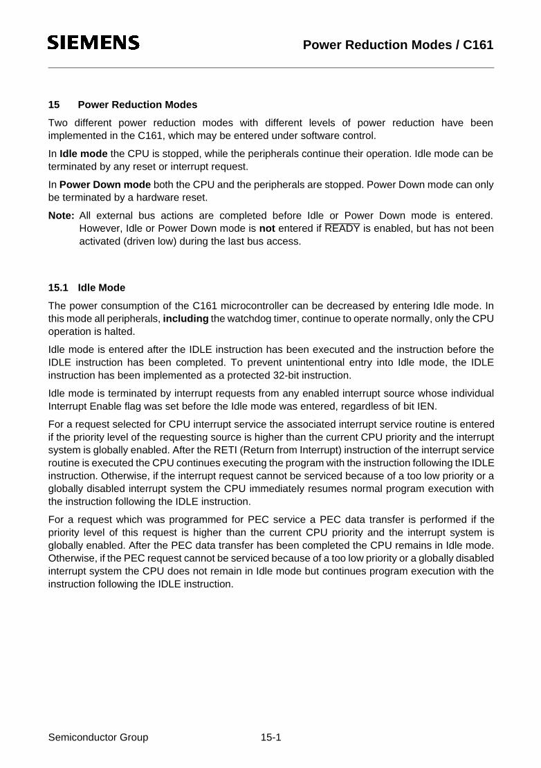
10Jul97@15:19h Power Reduction Modes / C161
15 Power Reduction Modes
Two different power reduction modes with different levels of power reduction have beenimplemented in the C161, which may be entered under software control.
In Idle mode the CPU is stopped, while the peripherals continue their operation. Idle mode can beterminated by any reset or interrupt request.
In Power Down mode both the CPU and the peripherals are stopped. Power Down mode can onlybe terminated by a hardware reset.
Note: All external bus actions are completed before Idle or Power Down mode is entered.However, Idle or Power Down mode is not entered if READY is enabled, but has not beenactivated (driven low) during the last bus access.
15.1 Idle Mode
The power consumption of the C161 microcontroller can be decreased by entering Idle mode. Inthis mode all peripherals, including the watchdog timer, continue to operate normally, only the CPUoperation is halted.
Idle mode is entered after the IDLE instruction has been executed and the instruction before theIDLE instruction has been completed. To prevent unintentional entry into Idle mode, the IDLEinstruction has been implemented as a protected 32-bit instruction.
Idle mode is terminated by interrupt requests from any enabled interrupt source whose individualInterrupt Enable flag was set before the Idle mode was entered, regardless of bit IEN.
For a request selected for CPU interrupt service the associated interrupt service routine is enteredif the priority level of the requesting source is higher than the current CPU priority and the interruptsystem is globally enabled. After the RETI (Return from Interrupt) instruction of the interrupt serviceroutine is executed the CPU continues executing the program with the instruction following the IDLEinstruction. Otherwise, if the interrupt request cannot be serviced because of a too low priority or aglobally disabled interrupt system the CPU immediately resumes normal program execution withthe instruction following the IDLE instruction.
For a request which was programmed for PEC service a PEC data transfer is performed if thepriority level of this request is higher than the current CPU priority and the interrupt system isglobally enabled. After the PEC data transfer has been completed the CPU remains in Idle mode.Otherwise, if the PEC request cannot be serviced because of a too low priority or a globally disabledinterrupt system the CPU does not remain in Idle mode but continues program execution with theinstruction following the IDLE instruction.
Semiconductor Group 15-1
10Jul97@15:19h Power Reduction Modes / C161
Figure 15-1Transitions between Idle mode and active mode
Idle mode can also be terminated by a Non-Maskable Interrupt, ie. a high to low transition on theNMI pin. After Idle mode has been terminated by an interrupt or NMI request, the interrupt systemperforms a round of prioritization to determine the highest priority request. In the case of an NMIrequest, the NMI trap will always be entered.
Any interrupt request whose individual Interrupt Enable flag was set before Idle mode was enteredwill terminate Idle mode regardless of the current CPU priority. The CPU will not go back into Idlemode when a CPU interrupt request is detected, even when the interrupt was not serviced becauseof a higher CPU priority or a globally disabled interrupt system (IEN=’0’). The CPU will only go backinto Idle mode when the interrupt system is globally enabled (IEN=’1’) and a PEC service on apriority level higher than the current CPU level is requested and executed.
Note: An interrupt request which is individually enabled and assigned to priority level 0 willterminate Idle mode. The associated interrupt vector will not be accessed, however.
The watchdog timer may be used to monitor the Idle mode: an internal reset will be generated if nointerrupt or NMI request occurs before the watchdog timer overflows. To prevent the watchdog timerfrom overflowing during Idle mode it must be programmed to a reasonable time interval before Idlemode is entered.
Semiconductor Group 15-2

10Jul97@15:19h Power Reduction Modes / C161
15.2 Power Down Mode
To further reduce the power consumption the microcontroller can be switched to Power Downmode. Clocking of all internal blocks is stopped, the contents of the internal RAM, however, arepreserved through the voltage supplied via the VCC pins. The watchdog timer is stopped in PowerDown mode. This mode can only be terminated by an external hardware reset, ie. by asserting a lowlevel on the RSTIN pin. This reset will initialize all SFRs and ports to their default state, but will notchange the contents of the internal RAM.
There are two levels of protection against unintentionally entering Power Down mode. First, thePWRDN (Power Down) instruction which is used to enter this mode has been implemented as aprotected 32-bit instruction. Second, this instruction is effective only if the NMI (Non MaskableInterrupt) pin is externally pulled low while the PWRDN instruction is executed. The microcontrollerwill enter Power Down mode after the PWRDN instruction has completed.
This feature can be used in conjunction with an external power failure signal which pulls the NMI pinlow when a power failure is imminent. The microcontroller will enter the NMI trap routine which cansave the internal state into RAM. After the internal state has been saved, the trap routine may seta flag or write a certain bit pattern into specific RAM locations, and then execute the PWRDNinstruction. If the NMI pin is still low at this time, Power Down mode will be entered, otherwiseprogram execution continues. During power down the voltage at the VCC pins can be lowered to2.5 V while the contents of the internal RAM will still be preserved.
The initialization routine (executed upon reset) can check the identification flag or bit pattern withinRAM to determine whether the controller was initially switched on, or whether it was properlyrestarted from Power Down mode.
Semiconductor Group 15-3
10Jul97@15:19h Power Reduction Modes / C161
15.3 Status of Output Pins during Idle and Power Down Mode
During Idle mode the CPU clocks are turned off, while all peripherals continue their operation in thenormal way. Therefore all ports pins, which are configured as general purpose output pins, outputthe last data value which was written to their port output latches. If the alternate output function ofa port pin is used by a peripheral, the state of the pin is determined by the operation of theperipheral.
Port pins which are used for bus control functions go into that state which represents the inactivestate of the respective function (eg. WR), or to a defined state which is based on the last bus access(eg. BHE). Port pins which are used as external address/data bus hold the address/data which wasoutput during the last external memory access before entry into Idle mode under the followingconditions:
P0H outputs the high byte of the last address if a multiplexed bus mode with 8-bit data bus is used,otherwise P0H is floating. P0L is always floating in Idle mode.
PORT1 outputs the lower 16 bits of the last address if a demultiplexed bus mode is used, otherwisethe output pins of PORT1 represent the port latch data.
Port 4 outputs the segment address for the last access on those pins that were selected duringreset, otherwise the output pins of Port 4 represent the port latch data.
During Power Down mode the oscillator and the clocks to the CPU and to the peripherals areturned off. Like in Idle mode, all port pins which are configured as general purpose output pinsoutput the last data value which was written to their port output latches.
When the alternate output function of a port pin is used by a peripheral the state of this pin isdetermined by the last action of the peripheral before the clocks were switched off.
Semiconductor Group 15-4
10Jul97@15:19h Power Reduction Modes / C161
The table below summarizes the state of all C161 output pins during Idle and Power Down mode.
Note:1): High if EINIT was executed before entering Idle or Power Down mode, Low otherwise.2): For multiplexed buses with 8-bit data bus.3): For demultiplexed buses.4): The CS signal that corresponds to the last address remains active (low), all other enabled CSsignals remain inactive (high). By accessing an on-chip X-Periperal prior to entering a power savemode all external CS signals can be deactivated.
C161Output Pin(s)
Idle Mode Power Down Mode
Noexternal bus
External busenabled
Noexternal bus
External busenabled
ALE Low Low Low Low
RD, WR High High High High
RSTOUT 1) 1) 1) 1)
P0L Port Latch Data Floating Port Latch Data Floating
P0H Port Latch Data A15...A8 2) / Float Port Latch Data A15...A8 2) / Float
PORT1 Port Latch Data Last Address 3) /Port Latch Data
Port Latch Data Last Address 3) /Port Latch Data
Port 4 Port Latch Data Port Latch Data/Last segment
Port Latch Data Port Latch Data/Last segment
BHE Port Latch Data Last value Port Latch Data Last value
CSx Port Latch Data Last value 4) Port Latch Data Last value 4)
Other Port Output Pins
Port Latch Data / Alternate Function
Port Latch Data / Alternate Function
Port Latch Data / Alternate Function
Port Latch Data / Alternate Function
Semiconductor Group 15-5

10Jul97@15:19h System Programming / C161
16 System Programming
To aid in software development, a number of features has been incorporated into the instruction setof the C161, including constructs for modularity, loops, and context switching. In many casescommonly used instruction sequences have been simplified while providing greater flexibility. Thefollowing programming features help to fully utilize this instruction set.
Instructions Provided as Subsets of Instructions
In many cases, instructions found in other microcontrollers are provided as subsets of morepowerful instructions in the C161. This allows the same functionality to be provided whiledecreasing the hardware required and decreasing decode complexity. In order to aid assemblyprogramming, these instructions, familiar from other microcontrollers, can be built in macros, thusproviding the same names.
Directly Substitutable Instructions are instructions known from other microcontrollers that can bereplaced by the following instructions of the C161:
Modification of System Flags is performed using bit set or bit clear instructions (BSET, BCLR). Allbit and word instructions can access the PSW register, so no instructions like CLEAR CARRY orENABLE INTERRUPTS are required.
External Memory Data Access does not require special instructions to load data pointers orexplicitly load and store external data. The C161 provides a Von-Neumann memory architectureand its on-chip hardware automatically detects accesses to internal RAM, GPRs, and SFRs.
Multiplication and Division
Multiplication and division of words and double words is provided through multiple cycle instructionsimplementing a Booth algorithm. Each instruction implicitly uses the 32-bit register MD (MDL =lower 16 bits, MDH = upper 16 bits). The MDRIU flag (Multiply or Divide Register In Use) in registerMDC is set whenever either half of this register is written to or when a multiply/divide instruction isstarted. It is cleared whenever the MDL register is read. Because an interrupt can be acknowledgedbefore the contents of register MD are saved, this flag is required to alert interrupt routines, whichrequire the use of the multiply/divide hardware, so they can preserve register MD. This register,however, only needs to be saved when an interrupt routine requires use of the MD register and aprevious task has not saved the current result. This flag is easily tested by the Jump-on-Bitinstructions.
Substituted Instruction C161 Instruction Function
CLR Rn AND Rn, #0H Clear register
CPLB Bit BMOVN Bit, Bit Complement bit
DEC Rn SUB Rn, #1H Decrement register
INC Rn ADD Rn, #1H Increment register
SWAPB Rn ROR Rn, #8H Swap bytes within word
Semiconductor Group 16-1
10Jul97@15:19h System Programming / C161
Multiplication or division is simply performed by specifying the correct (signed or unsigned) versionof the multiply or divide instruction. The result is then stored in register MD. The overflow flag (V) isset if the result from a multiply or divide instruction is greater than 16 bits. This flag can be used todetermine whether both word halfs must be transferred from register MD. The high portion ofregister MD (MDH) must be moved into the register file or memory first, in order to ensure that theMDRIU flag reflects the correct state.
The following instruction sequence performs an unsigned 16 by 16-bit multiplication:
...SAVE: JNB MDRIU, START ;Test if MD was in use.
SCXT MDC, #0010H ;Save and clear control register, leaving MDRIU set;(only required for interrupted multiply/divide instructions)
BSET SAVED ;Indicate the save operationPUSH MDH ;Save previous MD contents...PUSH MDL ;...on system stack
START: MULU R1, R2 ;Multiply 16·16 unsigned, Sets MDRIUJMPR cc_NV, COPYL ;Test for only 16-bit resultMOV R3, MDH ;Move high portion of MD
COPYL: MOV R4, MDL ;Move low portion of MD, Clears MDRIURESTORE: JNB SAVED, DONE ;Test if MD registers were saved
POP MDL ;Restore registersPOP MDHPOP MDCBCLR SAVED ;Multiplication is completed, program continues
DONE: ...
The above save sequence and the restore sequence after COPYL are only required if the currentroutine could have interrupted a previous routine which contained a MUL or DIV instruction.Register MDC is also saved because it is possible that a previous routine's Multiply or Divideinstruction was interrupted while in progress. In this case the information about how to restart theinstruction is contained in this register. Register MDC must be cleared to be correctly initialized fora subsequent multiplication or division. The old MDC contents must be popped from the stackbefore the RETI instruction is executed.
For a division the user must first move the dividend into the MD register. If a 16/16-bit division isspecified, only the low portion of register MD must be loaded. The result is also stored into registerMD. The low portion (MDL) contains the integer result of the division, while the high portion (MDH)contains the remainder.
Semiconductor Group 16-2

10Jul97@15:19h System Programming / C161
The following instruction sequence performs a 32 by 16-bit division:
MOV MDH, R1 ;Move dividend to MD register. Sets MDRIUMOV MDL, R2 ;Move low portion to MDDIV R3 ;Divide 32/16 signed, R3 holds the divisorJMPR cc_V, ERROR ;Test for divide overflowMOV R3, MDH ;Move remainder to R3MOV R4, MDL ;Move integer result to R4. Clears MDRIU
Whenever a multiply or divide instruction is interrupted while in progress, the address of theinterrupted instruction is pushed onto the stack and the MULIP flag in the PSW of the interruptingroutine is set. When the interrupt routine is exited with the RETI instruction, this bit is implicitly testedbefore the old PSW is popped from the stack. If MULIP=’1’ the multiply/divide instruction is re-readfrom the location popped from the stack (return address) and will be completed after the RETIinstruction has been executed.
Note: The MULIP flag is part of the context of the interrupted task. When the interrupting routinedoes not return to the interrupted task (eg. scheduler switches to another task) the MULIPflag must be set or cleared according to the context of the task that is switched to.
BCD Calculations
No direct support for BCD calculations is provided in the C161. BCD calculations are performed byconverting BCD data to binary data, performing the desired calculations using standard data types,and converting the result back to BCD data. Due to the enhanced performance of divisioninstructions binary data is quickly converted to BCD data through division by 10D. Conversion fromBCD data to binary data is enhanced by multiple bit shift instructions. This provides similarperformance compared to instructions directly supporting BCD data types, while no additionalhardware is required.
Semiconductor Group 16-3

10Jul97@15:19h System Programming / C161
16.1 Stack Operations
The C161 supports two types of stacks. The system stack is used implicitly by the controller and islocated in the internal RAM. The user stack provides stack access to the user in either the internalor external memory. Both stack types grow from high memory addresses to low memory addresses.
Internal System Stack
A system stack is provided to store return vectors, segment pointers, and processor status forprocedures and interrupt routines. A system register, SP, points to the top of the stack. This pointeris decremented when data is pushed onto the stack, and incremented when data is popped.
The internal system stack can also be used to temporarily store data or pass it between subroutinesor tasks. Instructions are provided to push or pop registers on/from the system stack. However, inmost cases the register banking scheme provides the best performance for passing data betweenmultiple tasks.
Note: The system stack allows the storage of words only. Bytes must either be converted to wordsor the respective other byte must be disregarded.Register SP can only be loaded with even byte addresses (The LSB of SP is always ’0’).
Detection of stack overflow/underflow is supported by two registers, STKOV (Stack OverflowPointer) and STKUN (Stack Underflow Pointer). Specific system traps (Stack Overflow trap, StackUnderflow trap) will be entered whenever the SP reaches either boundary specified in theseregisters.
The contents of the stack pointer are compared to the contents of the overflow register, wheneverthe SP is DECREMENTED either by a CALL, PUSH or SUB instruction. An overflow trap will beentered, when the SP value is less than the value in the stack overflow register.
The contents of the stack pointer are compared to the contents of the underflow register, wheneverthe SP is INCREMENTED either by a RET, POP or ADD instruction. An underflow trap will beentered, when the SP value is greater than the value in the stack underflow register.
Note: When a value is MOVED into the stack pointer, NO check against the overflow/underflowregisters is performed.
In many cases the user will place a software reset instruction (SRST) into the stack underflow andoverflow trap service routines. This is an easy approach, which does not require specialprogramming. However, this approach assumes that the defined internal stack is sufficient for thecurrent software and that exceeding its upper or lower boundary represents a fatal error.
It is also possible to use the stack underflow and stack overflow traps to cache portions of a largerexternal stack. Only the portion of the system stack currently being used is placed into the internalmemory, thus allowing a greater portion of the internal RAM to be used for program, data or registerbanking. This approach assumes no error but requires a set of control routines (see below).
Semiconductor Group 16-4
10Jul97@15:19h System Programming / C161
Circular (virtual) Stack
This basic technique allows pushing until the overflow boundary of the internal stack is reached. Atthis point a portion of the stacked data must be saved into external memory to create space forfurther stack pushes. This is called “stack flushing”. When executing a number of return or popinstructions, the upper boundary (since the stack empties upward to higher memory locations) isreached. The entries that have been previously saved in external memory must now be restored.This is called “stack filling”. Because procedure call instructions do not continue to nest infinitely andcall and return instructions alternate, flushing and filling normally occurs very infrequently. If this isnot true for a given program environment, this technique should not be used because of theoverhead of flushing and filling.
The basic mechanism is the transformation of the addresses of a virtual stack area, controlled viaregisters SP, STKOV and STKUN, to a defined physical stack area within the internal RAM viahardware. This virtual stack area covers all possible locations that SP can point to, ie. 00’F000Hthrough 00’FFFEH. STKOV and STKUN accept the same 4 KByte address range.The size of the physical stack area within the internal RAM that effectively is used for standard stackoperations is defined via bitfield STKSZ in register SYSCON (see below).
The virtual stack addresses are transformed to physical stack addresses by concatenating thesignificant bits of the stack pointer register SP (see table) with the complementary most significantbits of the upper limit of the physical stack area (00’FBFEH). This transformation is done viahardware (see figure below).
The reset values (STKOV=FA00H, STKUN=FC00H, SP=FC00H, STKSZ=000B) map the virtualstack area directly to the physical stack area and allow using the internal system stack without anychanges, provided that the 256 word area is not exceeded.
<STKSZ> Stack Size (Words)
Internal RAM Addresses (Words)of Physical Stack
Significant Bits of Stack Pointer SP
0 0 0 B 256 00’FBFEH...00’FA00H (Default after Reset) SP.8...SP.0
0 0 1 B 128 00’FBFEH...00’FB00H SP.7...SP.0
0 1 0 B 64 00’FBFEH...00’FB80H SP.6...SP.0
0 1 1 B 32 00’FBFEH...00’FBC0H SP.5...SP.0
1 0 0 B 512 00’FBFEH...00’F800H (not for 1KByte IRAM) SP.9...SP.0
1 0 1 B --- Reserved. Do not use this combination. ---
1 1 0 B --- Reserved. Do not use this combination. ---
1 1 1 B 1024 00’FDFEH...00’FX00H (Note: No circular stack)00’FX00H represents the lower IRAM limit, ie.1 KB: 00’FA00H, 2 KB: 00’F600H, 3 KB: 00’F200H
SP.11...SP.0
Semiconductor Group 16-5

10Jul97@15:19h System Programming / C161
Figure 16-1Physical Stack Address Generation
The following example demonstrates the circular stack mechanism which is also an effect of thisvirtual stack mapping: First, register R1 is pushed onto the lowest physical stack location accordingto the selected maximum stack size. With the following instruction, register R2 will be pushed ontothe highest physical stack location although the SP is decremented by 2 as for the previous pushoperation.
MOV SP, #0F802H ; Set SP before last entry of physical stack of 256 words... ; (SP) = F802H: Physical stack address = FA02HPUSH R1 ; (SP) = F800H: Physical stack address = FA00HPUSH R2 ; (SP) = F7FEH: Physical stack address = FBFEH
The effect of the address transformation is that the physical stack addresses wrap around from theend of the defined area to its beginning. When flushing and filling the internal stack, this circularstack mechanism only requires to move that portion of stack data which is really to be re-used (ie.the upper part of the defined stack area) instead of the whole stack area. Stack data that remain inthe lower part of the internal stack need not be moved by the distance of the space being flushedor filled, as the stack pointer automatically wraps around to the beginning of the freed part of thestack area.
Note: This circular stack technique is applicable for stack sizes of 32 to 512 words (STKSZ = ‘000B’to ‘100B’), it does not work with option STKSZ = ‘111B’, which uses the complete internalRAM for system stack.In the latter case the address transformation mechanism is deactivated.
1 1 1 1 1 0 1 1 1 1 1 1 1 1 1 0
1 1 1 1 1 0 1 1 1 0 0 0 0 0 0 0
1 1 1 1 1 0 1 1 1 0 0 0 0 0 0 0 1 1 1 1 1 0 1 0 0 0 0 0 0 0 0 0
1 1 1 1 1 0 1 1 1 1 1 1 1 1 1 0
1 1 1 1 1 0 1 1 0 1 1 1 1 1 1 0
1 1 1 1 1 0 1 1 1 1 1 1 1 1 1 0
FBFEH
FB80H
FB80H
FBFEH
FB7EH
FBFEH
FBFEH
64 words 256 words
F800H 1 1 1 1 1 0 0 0 0 0 0 0 0 0 0 0
FA00H
1 1 1 1 0 1 1 1 1 1 1 1 1 1 1 0
1 1 1 1 1 0 1 1 1 1 1 1 1 1 1 0
FBFEH
F7FEH
FBFEH
1 1 1 1 1 0 1 1 1 1 1 1 1 1 1 0
1 1 1 1 1 0 1 1 1 1 1 1 1 1 1 0
<SP>
<SP>
Phys.A.
Phys.A.
Stack Size
After PUSH After PUSH
Semiconductor Group 16-6
10Jul97@15:19h System Programming / C161
When a boundary is reached, the stack underflow or overflow trap is entered, where the user movesa predetermined portion of the internal stack to or from the external stack. The amount of datatransferred is determined by the average stack space required by routines and the frequency ofcalls, traps, interrupts and returns. In most cases this will be approximately one quarter to one tenththe size of the internal stack. Once the transfer is complete, the boundary pointers are updated toreflect the newly allocated space on the internal stack. Thus, the user is free to write code withoutconcern for the internal stack limits. Only the execution time required by the trap routines affectsuser programs.
The following procedure initializes the controller for usage of the circular stack mechanism:
• Specify the size of the physical system stack area within the internal RAM (bitfield STKSZ inregister SYSCON).
• Define two pointers, which specify the upper and lower boundary of the external stack. Thesevalues are then tested in the stack underflow and overflow trap routines when moving data.
• Set the stack overflow pointer (STKOV) to the limit of the defined internal stack area plus six words(for the reserved space to store two interrupt entries).
The internal stack will now fill until the overflow pointer is reached. After entry into the overflow trapprocedure, the top of the stack will be copied to the external memory. The internal pointers will thenbe modified to reflect the newly allocated space. After exiting from the trap procedure, the internalstack will wrap around to the top of the internal stack, and continue to grow until the new value ofthe stack overflow pointer is reached.
When the underflow pointer is reached while the stack is meptied the bottom of stack is reloadedfrom the external memory and the internal pointers are adjusted accordingly.
Linear Stack
The C161 also offers a linear stack option (STKSZ = ‘111B’), where the system stack may use thecomplete internal RAM area. This provides a large system stack without requiring procedures tohandle data transfers for a circular stack. However, this method also leaves less RAM space forvariables or code. The RAM area that may effectively be consumed by the system stack is definedvia the STKUN and STKOV pointers. The underflow and overflow traps in this case serve for fatalerror detection only.
For the linear stack option all modifiable bits of register SP are used to access the physical stack.Although the stack pointer may cover addresses from 00’F000H up to 00’FFFEH the (physical)system stack must be located within the internal RAM and therefore may only use the addressrange 00’F600H to 00’FDFEH. It is the user’s responsibility to restrict the system stack to the internalRAM range.
Note: Avoid stack accesses below the IRAM area (ESFR space and reserved area) and withinaddress range 00’FE00H and 00’FFFEH (SFR space).Otherwise unpredictable results will occur.
Semiconductor Group 16-7
10Jul97@15:19h System Programming / C161
User Stacks
User stacks provide the ability to create task specific data stacks and to off-load data from thesystem stack. The user may push both bytes and words onto a user stack, but is responsible forusing the appropriate instructions when popping data from the specific user stack. No hardwaredetection of overflow or underflow of a user stack is provided. The following addressing modesallow implementation of user stacks:
[– Rw], Rb or [– Rw], Rw : Pre-decrement Indirect Addressing.Used to push one byte or word onto a user stack. This mode is only available for MOV instructionsand can specify any GPR as the user stack pointer.
Rb, [Rw+] or Rw, [Rw+] : Post-increment Index Register Indirect Addressing.Used to pop one byte or word from a user stack. This mode is available to most instructions, but onlyGPRs R0-R3 can be specified as the user stack pointer.
Rb, [Rw+] or Rw, [Rw+] : Post-increment Indirect Addressing.Used to pop one byte or word from a user stack. This mode is only available for MOV instructionsand can specify any GPR as the user stack pointer.
16.2 Register Banking
Register banking provides the user with an extremely fast method to switch user context. A singlemachine cycle instruction saves the old bank and enters a new register bank. Each register bankmay assign up to 16 registers. Each register bank should be allocated during coding based on theneeds of each task. Once the internal memory has been partitioned into a register bank space,internal stack space and a global internal memory area, each bank pointer is then assigned. Thus,upon entry into a new task, the appropriate bank pointer is used as the operand for the SCXT(switch context) instruction. Upon exit from a task a simple POP instruction to the context pointer(CP) restores the previous task’s register bank.
16.3 Procedure Call Entry and Exit
To support modular programming a procedure mechanism is provided to allow coding of frequentlyused portions of code into subroutines. The CALL and RET instructions store and restore the valueof the instruction pointer (IP) on the system stack before and after a subroutine is executed.
Procedures may be called conditionally with instructions CALLA or CALLI, or be calledunconditionally using instructions CALLR or CALLS.
Note: Any data pushed onto the system stack during execution of the subroutine must be poppedbefore the RET instruction is executed.
Semiconductor Group 16-8

10Jul97@15:19h System Programming / C161
Passing Parameters on the System Stack
Parameters may be passed via the system stack through PUSH instructions before the subroutineis called, and POP instructions during execution of the subroutine. Base plus offset indirectaddressing also permits access to parameters without popping these parameters from the stackduring execution of the subroutine. Indirect addressing provides a mechanism of accessing datareferenced by data pointers, which are passed to the subroutine.
In addition, two instructions have been implemented to allow one parameter to be passed on thesystem stack without additional software overhead.
The PCALL (push and call) instruction first pushes the ’reg’ operand and the IP contents onto thesystem stack and then passes control to the subroutine specified by the ’caddr’ operand.
When exiting from the subroutine, the RETP (return and pop) instruction first pops the IP and thenthe ’reg’ operand from the system stack and returns to the calling program.
Cross Segment Subroutine Calls
Calls to subroutines in different segments require the use of the CALLS (call inter-segmentsubroutine) instruction. This instruction preserves both the CSP (code segment pointer) and IP onthe system stack.
Upon return from the subroutine, a RETS (return from inter-segment subroutine) instruction must beused to restore both the CSP and IP. This ensures that the next instruction after the CALLSinstruction is fetched from the correct segment.
Note: It is possible to use CALLS within the same segment, but still two words of the stack areused to store both the IP and CSP.
Providing Local Registers for Subroutines
For subroutines which require local storage, the following methods are provided:
Alternate Bank of Registers: Upon entry into a subroutine, it is possible to specify a new set oflocal registers by executing the SCXT (switch context) instruction. This mechanism does notprovide a method to recursively call a subroutine.
Saving and Restoring of Registers: To provide local registers, the contents of the registers whichare required for use by the subroutine can be pushed onto the stack and the previous values bepopped before returning to the calling routine. This is the most common technique used today andit does provide a mechanism to support recursive procedures. This method, however, requires twomachine cycles per register stored on the system stack (one cycle to PUSH the register, and one toPOP the register).
Use of the System Stack for Local Registers: It is possible to use the SP and CP to set up localsubroutine register frames. This enables subroutines to dynamically allocate local variables asneeded within two machine cycles. A local frame is allocated by simply subtracting the number ofrequired local registers from the SP, and then moving the value of the new SP to the CP.
Semiconductor Group 16-9

10Jul97@15:19h System Programming / C161
This operation is supported through the SCXT (switch context) instruction with the addressing mode’reg, mem’. Using this instruction saves the old contents of the CP on the system stack and movesthe value of the SP into CP (see example below). Each local register is then accessed as if it wasa normal register. Upon exit from the subroutine, first the old CP must be restored by popping it fromthe stack and then the number of used local registers must be added to the SP to restore theallocated local space back to the system stack.
Note: The system stack is growing downwards, while the register bank is growing upwards.
Figure 16-2Local Registers
The software to provide the local register bank for the example above is very compact:
After entering the subroutine:
SUB SP, #10D ; Free 5 words in the current system stackSCXT CP, SP ; Set the new register bank pointer
Before exiting the subroutine:
POP CP ; Restore the old register bankADD SP, #10D ; Release the 5 word of the current system stack
Old Stack Area
NewlyAllocated Register
Bank
R4R3R2R1R0
Old CP Contents
Old SP
New SPNew CP
New Stack Area
Semiconductor Group 16-10
10Jul97@15:19h System Programming / C161
16.4 Table Searching
A number of features have been included to decrease the execution time required to search tables.First, branch delays are eliminated by the branch target cache after the first iteration of the loop.Second, in non-sequentially searched tables, the enhanced performance of the ALU allows morecomplicated hash algorithms to be processed to obtain better table distribution. For sequentiallysearched tables, the auto-increment indirect addressing mode and the E (end of table) flag storedin the PSW decrease the number of overhead instructions executed in the loop.
The two examples below illustrate searching ordered tables and non-ordered tables, respectively:
MOV R0, #BASE ;Move table base into R0LOOP: CMP R1, [R0+] ;Compare target to table entry
JMPR cc_SGT, LOOP ;Test whether target has not been found
Note: The last entry in the table must be greater than the largest possible target.
MOV R0, #BASE ;Move table base into R0LOOP: CMP R1, [R0+] ;Compare target to table entry
JMPR cc_NET, LOOP ;Test whether target is not found AND the end of table...;...has not been reached.
Note: The last entry in the table must be equal to the lowest signed integer (8000H).
16.5 Peripheral Control and Interface
All communication between peripherals and the CPU is performed either by PEC transfers to andfrom internal memory, or by explicitly addressing the SFRs associated with the specific peripherals.After resetting the C161 all peripherals (except the watchdog timer) are disabled and initialized todefault values. A desired configuration of a specific peripheral is programmed using MOVinstructions of either constants or memory values to specific SFRs. Specific control flags may alsobe altered via bit instructions.
Once in operation, the peripheral operates autonomously until an end condition is reached at whichtime it requests a PEC transfer or requests CPU servicing through an interrupt routine. Informationmay also be polled from peripherals through read accesses to SFRs or bit operations includingbranch tests on specific control bits in SFRs. To ensure proper allocation of peripherals amongmultiple tasks, a portion of the internal memory has been made bit addressable to allow usersemaphores. Instructions have also been provided to lock out tasks via software by setting orclearing user specific bits and conditionally branching based on these specific bits.
It is recommended that bit fields in control SFRs are updated using the BFLDH and BFLDLinstructions or a MOV instruction to avoid undesired intermediate modes of operation which canoccur, when BCLR/BSET or AND/OR instruction sequences are used.
Semiconductor Group 16-11
10Jul97@15:19h System Programming / C161
16.6 Floating Point Support
All floating point operations are performed using software. Standard multiple precision instructionsare used to perform calculations on data types that exceed the size of the ALU. Multiple bit rotateand logic instructions allow easy masking and extracting of portions of floating point numbers.
To decrease the time required to perform floating point operations, two hardware features havebeen implemented in the CPU core. First, the PRIOR instruction aids in normalizing floating pointnumbers by indicating the position of the first set bit in a GPR. This result can the be used to rotatethe floating point result accordingly. The second feature aids in properly rounding the result ofnormalized floating point numbers through the overflow (V) flag in the PSW. This flag is set when aone is shifted out of the carry bit during shift right operations. The overflow flag and the carry flag arethen used to round the floating point result based on the desired rounding algorithm.
16.7 Trap/Interrupt Entry and Exit
Interrupt routines are entered when a requesting interrupt has a priority higher than the current CPUpriority level. Traps are entered regardless of the current CPU priority. When either a trap orinterrupt routine is entered, the state of the machine is preserved on the system stack and a branchto the appropriate trap/interrupt vector is made.
All trap and interrupt routines require the use of the RETI (return from interrupt) instruction to exitfrom the called routine. This instruction restores the system state from the system stack and thenbranches back to the location where the trap or interrupt occurred.
16.8 Unseparable Instruction Sequences
The instructions of the C161 are very efficient (most instructions execute in one machine cycle) andeven the multiplication and division are interruptable in order to minimize the response latency tointerrupt requests (internal and external). In many microcontroller applications this is vital.
Some special occasions, however, require certain code sequences (eg. semaphore handling) to beuninterruptable to function properly. This can be provided by inhibiting interrupts during therespective code sequence by disabling and enabling them before and after the sequence. Thenecessary overhead may be reduced by means of the ATOMIC instruction which allows locking1...4 instructions to an unseparable code sequence, during which the interrupt system (standardinterrupts and PEC requests) and Class A Traps (NMI, stack overflow/underflow) are disabled. AClass B Trap (illegal opcode, illegal bus access, etc.), however, will interrupt the atomic sequence,since it indicates a severe hardware problem. The interrupt inhibit caused by an ATOMIC instructiongets active immediately, ie. no other instruction will enter the pipeline except the one that follows theATOMIC instruction, and no interrupt request will be serviced in between. All instructions requiringmultiple cycles or hold states are regarded as one instruction in this sense (eg. MUL is oneinstruction). Any instruction type can be used within an unseparable code sequence.
EXAMPLE: ATOMIC #3 ; The following 3 instructions are locked (No NOP required)MOV R0, #1234H ; Instruction 1 (no other instr. enters the pipeline!)MOV R1, #5678H ; Instruction 2MUL R0, R1 ; Instruction 3: MUL regarded as one instructionMOV R2, MDL ; This instruction is out of the scope
; of the ATOMIC instruction sequence
Semiconductor Group 16-12

10Jul97@15:19h System Programming / C161
16.9 Overriding the DPP Addressing Mechanism
The standard mechanism to access data locations uses one of the four data page pointers (DPPx),which selects a 16 KByte data page, and a 14-bit offset within this data page. The four DPPs allowimmediate access to up to 64 KByte of data. In applications with big data arrays, especially in HLLapplications using large memory models, this may require frequent reloading of the DPPs, even forsingle accesses.
The EXTP (extend page) instruction allows switching to an arbitrary data page for 1...4instructions without having to change the current DPPs.
EXAMPLE: EXTP R15, #1 ; The override page number is stored in R15MOV R0, [R14] ; The (14-bit) page offset is stored in R14MOV R1, [R13] ; This instruction uses the standard DPP scheme!
The EXTS (extend segment) instruction allows switching to a 64 KByte segment oriented dataaccess scheme for 1...4 instructions without having to change the current DPPs. In this case all 16bits of the operand address are used as segment offset, with the segment taken from the EXTSinstruction. This greatly simplifies address calculation with continuous data like huge arrays in “C”.
EXAMPLE: EXTS #15, #1 ; The override seg. is #15 (0F’0000H...0F’FFFFH)MOV R0, [R14] ; The (16-bit) segment offset is stored in R14MOV R1, [R13] ; This instruction uses the standard DPP scheme!
Note: Instructions EXTP and EXTS inhibit interrupts the same way as ATOMIC.
Short Addressing in the Extended SFR (ESFR) Space
The short addressing modes of the C161 (REG or BITOFF) implicitly access the SFR space. Theadditional ESFR space would have to be accessed via long addressing modes (MEM or [Rw]). TheEXTR (extend register) instruction redirects accesses in short addressing modes to the ESFRspace for 1...4 instructions, so the additional registers can be accessed this way, too.
The EXTPR and EXTSR instructions combine the DPP override mechanism with the redirection tothe ESFR space using a single instruction.
Note: Instructions EXTR, EXTPR and EXTSR inhibit interrupts the same way as ATOMIC.The switching to the ESFR area and data page overriding is checked by the developmenttools or handled automatically.
Nested Locked Sequences
Each of the described extension instruction and the ATOMIC instruction starts an internal“extension counter” counting the effected instructions. When another extension or ATOMICinstruction is contained in the current locked sequence this counter is restarted with the value of thenew instruction. This allows the construction of locked sequences longer than 4 instructions.
Note: • Interrupt latencies may be increased when using locked code sequences.• PEC requests are not serviced during idle mode, if the IDLE instruction is part of a lockedsequence.
Semiconductor Group 16-13
10Jul97@15:19h System Programming / C161
16.10 Handling the Internal ROM
The Mask-ROM or Flash versions of the C161 may provide and control a 32 KByte internal ROMarea that may store code as well as data. Access to this internal ROM area is controlled during thereset configuration and via software. The ROM area may be mapped to segment 0, to segment 1 ormay be disabled at all.
Note: The internal ROM area always occupies an address area of 32 KByte, even if theimplemented mask ROM or Flash memory is smaller than that (eg. 8 KByte).Of course the total implemented memory may exceed 32 KBytes.
ROM Configuration during Reset
The control input pin EA (External Access) enables the user to define the address area from whichthe first instructions after reset are fetched. When EA is low (‘0’) during reset, the internal ROM areais disabled and the first instructions are fetched from external memory. When EA is high (‘1’) duringreset, the internal ROM area is globally enabled and the first instructions are fetched from theinternal ROM.
Note: Be sure not to select internal ROM access after reset on ROMless devices.
Mapping the Internal ROM Area
After reset the internal ROM area is mapped into segment 0, the “system segment”(00’0000H...00’7FFFH) as a default. This is necessary to allow the first instructions to be fetchedfrom locations 00’0000H ff. The ROM area may be mapped to segment 1 (01’0000H...01’7FFFH) bysetting bit ROMS1 in register SYSCON. The internal ROM may now be accessed through the lowerhalf of segment 1, while accesses to segment 0 will now be made to external memory. This addsflexibility to the system software. The interrupt/trap vector table, which uses locations 00’0000Hthrough 00’01FFH, is now part of the external memory and may therefore be modified, ie. thesystem software may now change interrupt/trap handlers according to the current condition of thesystem. The internal ROM can still be used for fixed software routines like IO drivers, math libraries,application specific invariant routines, tables, etc. This combines the advantage of an integratednon-volatile memory with the advantage of a flexible, adaptable software system.
Enabling and Disabling the Internal ROM Area After Reset
If the internal ROM does not contain an appropriate startup code, the system may be booted fromexternal memory, while the internal ROM is enabled afterwards to provide access to library routines,tables, etc.
If the internal ROM only contains the startup code and/or test software, the system may be bootedfrom internal ROM, which may then be disabled, after the software has switched to executing from(eg.) external memory, in order to free the address space occupied by the internal ROM area, whichis now unnecessary.
Semiconductor Group 16-14

10Jul97@15:19h System Programming / C161
16.11 Pits, Traps and Mines
Although handling the internal ROM provides powerful means to enhance the overall performanceand flexibility of a system, extreme care must be taken in order to avoid a system crash. Instructionmemory is the most crucial resource for the C161 and it must be made sure that it never runs outof it. The following precautions help to take advantage of the methods mentioned above withoutjeopardizing system security.
Internal ROM access after reset: When the first instructions are to be fetched from internal ROM(EA=‘1’), the device must contain ROM memory, and the ROM must contain a valid reset vector andvalid code at its destination.
Mapping the internal ROM to segment 1: Due to instruction pipelining, any new ROM mappingwill at the earliest become valid for the second instruction after the instruction which has changedthe ROM mapping. To enable accesses to the ROM after mapping a branch to the newly selectedROM area (JMPS) and reloading of all data page pointers is required.This also applies to re-mapping the internal ROM to segment 0.
Enabling the internal ROM after reset: When enabling the internal ROM after having booted thesystem from external memory, note that the C161 will then access the internal ROM using thecurrent segment offset, rather than accessing external memory.
Disabling the internal ROM after reset: When disabling the internal ROM after having booted thesystem from there, note that the C161 will not access external memory before a jump to segment 0(in this case) is executed.
General Rules
When mapping the ROM no instruction or data accesses should be made to the internal ROM,otherwise unpredictable results may occur.
To avoid these problems, the instructions that configure the internal ROM should be executed fromexternal memory or from the internal RAM.
Whenever the internal ROM is disabled, enabled or remapped the DPPs must be explicitly(re)loaded to enable correct data accesses to the internal ROM and/or external memory.
Semiconductor Group 16-15

10Jul97@15:19h The Register Set / C161
17 The Register Set
This section summarizes all registers, which are implemented in the C161 and explains thedescription format which is used in the chapters describing the function and layout of the SFRs.For easy reference the registers are ordered according to two different keys (except for GPRs):
• Ordered by address, to check which register a given address references,
• Ordered by register name, to find the location of a specific register.
Register Description Format
In the respective chapters the function and the layout of the SFRs is described in a specific formatwhich provides a number of details about the described special function register. The examplebelow shows how to interpret these details.
A word register looks like this:
REG_NAME (A16H / A8H) E/SFR Reset Value: * * * *H
A byte register looks like this:
REG_NAME (A16H / A8H) E/SFR Reset Value: - - * *H
Elements:
REG_NAME Name of this registerA16 / A8 Long 16-bit address / Short 8-bit addressSFR/ESFR/XRegRegister space (SFR, ESFR or External/XBUS Register)(* *) * * Register contents after reset
0/1: defined value, ’X’: undefined, ’U’: unchanged (undefined (’X’) after power up)Bits that are set/cleared by hardware are marked with a shaded access box
Bit Function
bit(field)name Explanation of bit(field)nameDescription of the functions controlled by this bit(field).
5 4 3 2 1 011 10 9 8 7 615 14 13 12
rw rw- w rw r rw rw- - - -
res.res.res.res.res.writeonly
readonly bitfield bitfield
hwbit
stdbit
hwbit
5 4 3 2 1 011 10 9 8 7 615 14 13 12
rw rw- - - - rw rw- - - -
bitfieldbitfieldstdbit
hwbit
hwbit
Semiconductor Group 17-1
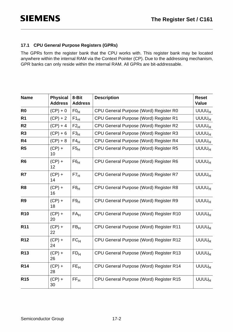
10Jul97@15:19h The Register Set / C161
17.1 CPU General Purpose Registers (GPRs)
The GPRs form the register bank that the CPU works with. This register bank may be locatedanywhere within the internal RAM via the Context Pointer (CP). Due to the addressing mechanism,GPR banks can only reside within the internal RAM. All GPRs are bit-addressable.
Name PhysicalAddress
8-BitAddress
Description ResetValue
R0 (CP) + 0 F0H CPU General Purpose (Word) Register R0 UUUUH
R1 (CP) + 2 F1H CPU General Purpose (Word) Register R1 UUUUH
R2 (CP) + 4 F2H CPU General Purpose (Word) Register R2 UUUUH
R3 (CP) + 6 F3H CPU General Purpose (Word) Register R3 UUUUH
R4 (CP) + 8 F4H CPU General Purpose (Word) Register R4 UUUUH
R5 (CP) + 10
F5H CPU General Purpose (Word) Register R5 UUUUH
R6 (CP) + 12
F6H CPU General Purpose (Word) Register R6 UUUUH
R7 (CP) + 14
F7H CPU General Purpose (Word) Register R7 UUUUH
R8 (CP) + 16
F8H CPU General Purpose (Word) Register R8 UUUUH
R9 (CP) + 18
F9H CPU General Purpose (Word) Register R9 UUUUH
R10 (CP) + 20
FAH CPU General Purpose (Word) Register R10 UUUUH
R11 (CP) + 22
FBH CPU General Purpose (Word) Register R11 UUUUH
R12 (CP) + 24
FCH CPU General Purpose (Word) Register R12 UUUUH
R13 (CP) + 26
FDH CPU General Purpose (Word) Register R13 UUUUH
R14 (CP) + 28
FEH CPU General Purpose (Word) Register R14 UUUUH
R15 (CP) + 30
FFH CPU General Purpose (Word) Register R15 UUUUH
Semiconductor Group 17-2

10Jul97@15:19h The Register Set / C161
The first 8 GPRs (R7...R0) may also be accessed bytewise. Other than with SFRs, writing to a GPRbyte does not affect the other byte of the respective GPR.The respective halves of the byte-accessible registers receive special names:
Name PhysicalAddress
8-BitAddress
Description ResetValue
RL0 (CP) + 0 F0H CPU General Purpose (Byte) Register RL0 UUH
RH0 (CP) + 1 F1H CPU General Purpose (Byte) Register RH0 UUH
RL1 (CP) + 2 F2H CPU General Purpose (Byte) Register RL1 UUH
RH1 (CP) + 3 F3H CPU General Purpose (Byte) Register RH1 UUH
RL2 (CP) + 4 F4H CPU General Purpose (Byte) Register RL2 UUH
RH2 (CP) + 5 F5H CPU General Purpose (Byte) Register RH2 UUH
RL3 (CP) + 6 F6H CPU General Purpose (Byte) Register RL3 UUH
RH3 (CP) + 7 F7H CPU General Purpose (Byte) Register RH3 UUH
RL4 (CP) + 8 F8H CPU General Purpose (Byte) Register RL4 UUH
RH4 (CP) + 9 F9H CPU General Purpose (Byte) Register RH4 UUH
RL5 (CP) + 10
FAH CPU General Purpose (Byte) Register RL5 UUH
RH5 (CP) + 11
FBH CPU General Purpose (Byte) Register RH5 UUH
RL6 (CP) + 12
FCH CPU General Purpose (Byte) Register RL6 UUH
RH6 (CP) + 13
FDH CPU General Purpose (Byte) Register RH6 UUH
RL7 (CP) + 14
FEH CPU General Purpose (Byte) Register RL7 UUH
RH7 (CP) + 14
FFH CPU General Purpose (Byte) Register RH7 UUH
Semiconductor Group 17-3

10Jul97@15:19h The Register Set / C161
17.2 Special Function Registers ordered by Name
The following table lists all SFRs which are implemented in the C161 in alphabetical order.Bit-addressable SFRs are marked with the letter “b” in column “Name”.SFRs within the Extended SFR-Space (ESFRs) are marked with the letter “E” in column “PhysicalAddress”. Registers within on-chip X-Peripherals (SSP) are marked with the letter “X” in column“Physical Address”.Registers which are unique to specific C161 derivatives are shaded.
Name PhysicalAddress
8-BitAddress
Description ResetValue
ADDRSEL1 FE18H 0CH Address Select Register 1 0000H
ADDRSEL2 FE1AH 0DH Address Select Register 2 0000H
ADDRSEL3 FE1CH 0EH Address Select Register 3 0000H
ADDRSEL4 FE1EH 0FH Address Select Register 4 0000H
BUSCON0 b FF0CH 86H Bus Configuration Register 0 0000H
BUSCON1 b FF14H 8AH Bus Configuration Register 1 0000H
BUSCON2 b FF16H 8BH Bus Configuration Register 2 0000H
BUSCON3 b FF18H 8CH Bus Configuration Register 3 0000H
BUSCON4 b FF1AH 8DH Bus Configuration Register 4 0000H
CAPREL FE4AH 25H GPT2 Capture/Reload Register 0000H
CC9IC b FF8AH C5H External Interrupt 1 Control Register 0000H
CC10IC b FF8CH C6H External Interrupt 2 Control Register 0000H
CC11IC b FF8EH C7H External Interrupt 3 Control Register 0000H
CC12IC b FF90H C8H External Interrupt 4 Control Register 0000H
CC13IC b FF92H C9H External Interrupt 5 Control Register 0000H
CC14IC b FF94H CAH External Interrupt 6 Control Register 0000H
CC15IC b FF96H CBH External Interrupt 7 Control Register 0000H
CP FE10H 08H CPU Context Pointer Register FC00H
CRIC b FF6AH B5H GPT2 CAPREL Interrupt Control Register 0000H
CSP FE08H 04H CPU Code Segment Pointer Register(8 bits, not directly writeable)
0000H
DP0L b F100H E 80H P0L Direction Control Register 00H
DP0H b F102H E 81H P0H Direction Control Register 00H
DP1L b F104H E 82H P1L Direction Control Register 00H
DP1H b F106H E 83H P1H Direction Control Register 00H
DP2 b FFC2H E1H Port 2 Direction Control Register 0000H
Semiconductor Group 17-4
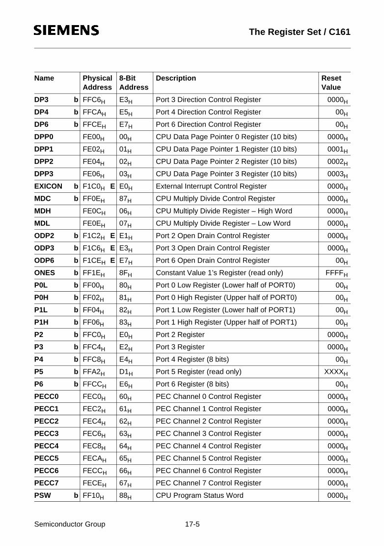
10Jul97@15:19h The Register Set / C161
DP3 b FFC6H E3H Port 3 Direction Control Register 0000H
DP4 b FFCAH E5H Port 4 Direction Control Register 00H
DP6 b FFCEH E7H Port 6 Direction Control Register 00H
DPP0 FE00H 00H CPU Data Page Pointer 0 Register (10 bits) 0000H
DPP1 FE02H 01H CPU Data Page Pointer 1 Register (10 bits) 0001H
DPP2 FE04H 02H CPU Data Page Pointer 2 Register (10 bits) 0002H
DPP3 FE06H 03H CPU Data Page Pointer 3 Register (10 bits) 0003H
EXICON b F1C0H E E0H External Interrupt Control Register 0000H
MDC b FF0EH 87H CPU Multiply Divide Control Register 0000H
MDH FE0CH 06H CPU Multiply Divide Register – High Word 0000H
MDL FE0EH 07H CPU Multiply Divide Register – Low Word 0000H
ODP2 b F1C2H E E1H Port 2 Open Drain Control Register 0000H
ODP3 b F1C6H E E3H Port 3 Open Drain Control Register 0000H
ODP6 b F1CEH E E7H Port 6 Open Drain Control Register 00H
ONES b FF1EH 8FH Constant Value 1’s Register (read only) FFFFH
P0L b FF00H 80H Port 0 Low Register (Lower half of PORT0) 00H
P0H b FF02H 81H Port 0 High Register (Upper half of PORT0) 00H
P1L b FF04H 82H Port 1 Low Register (Lower half of PORT1) 00H
P1H b FF06H 83H Port 1 High Register (Upper half of PORT1) 00H
P2 b FFC0H E0H Port 2 Register 0000H
P3 b FFC4H E2H Port 3 Register 0000H
P4 b FFC8H E4H Port 4 Register (8 bits) 00H
P5 b FFA2H D1H Port 5 Register (read only) XXXXH
P6 b FFCCH E6H Port 6 Register (8 bits) 00H
PECC0 FEC0H 60H PEC Channel 0 Control Register 0000H
PECC1 FEC2H 61H PEC Channel 1 Control Register 0000H
PECC2 FEC4H 62H PEC Channel 2 Control Register 0000H
PECC3 FEC6H 63H PEC Channel 3 Control Register 0000H
PECC4 FEC8H 64H PEC Channel 4 Control Register 0000H
PECC5 FECAH 65H PEC Channel 5 Control Register 0000H
PECC6 FECCH 66H PEC Channel 6 Control Register 0000H
PECC7 FECEH 67H PEC Channel 7 Control Register 0000H
PSW b FF10H 88H CPU Program Status Word 0000H
Name PhysicalAddress
8-BitAddress
Description ResetValue
Semiconductor Group 17-5

10Jul97@15:19h The Register Set / C161
RP0H b F108H E 84H System Startup Configuration Register (Rd. only) XXH
S0BG FEB4H 5AH Serial Channel 0 Baud Rate Generator Reload Register
0000H
S0CON b FFB0H D8H Serial Channel 0 Control Register 0000H
S0EIC b FF70H B8H Serial Channel 0 Error Interrupt Control Register 0000H
S0RBUF FEB2H 59H Serial Channel 0 Receive Buffer Register(read only)
XXXXH
S0RIC b FF6EH B7H Serial Channel 0 Receive Interrupt Control Register
0000H
S0TBIC b F19CH E CEH Serial Channel 0 Transmit Buffer Interrupt Control Register
0000H
S0TBUF FEB0H 58H Serial Channel 0 Transmit Buffer Register(write only)
0000H
S0TIC b FF6CH B6H Serial Channel 0 Transmit Interrupt Control Register
0000H
SP FE12H 09H CPU System Stack Pointer Register FC00H
SSCBR F0B4H E 5AH SSC Baudrate Register 0000H
SSCCON b FFB2H D9H SSC Control Register 0000H
SSCEIC b FF76H BBH SSC Error Interrupt Control Register 0000H
SSCRB F0B2H E 59H SSC Receive Buffer (read only) XXXXH
SSCRIC b FF74H BAH SSC Receive Interrupt Control Register 0000H
SSCTB F0B0H E 58H SSC Transmit Buffer (write only) 0000H
SSCTIC b FF72H B9H SSC Transmit Interrupt Control Register 0000H
STKOV FE14H 0AH CPU Stack Overflow Pointer Register FA00H
STKUN FE16H 0BH CPU Stack Underflow Pointer Register FC00H
SYSCON b FF12H 89H CPU System Configuration Register 0XX0H1)
T2 FE40H 20H GPT1 Timer 2 Register 0000H
T2CON b FF40H A0H GPT1 Timer 2 Control Register 0000H
T2IC b FF60H B0H GPT1 Timer 2 Interrupt Control Register 0000H
T3 FE42H 21H GPT1 Timer 3 Register 0000H
T3CON b FF42H A1H GPT1 Timer 3 Control Register 0000H
T3IC b FF62H B1H GPT1 Timer 3 Interrupt Control Register 0000H
T4 FE44H 22H GPT1 Timer 4 Register 0000H
T4CON b FF44H A2H GPT1 Timer 4 Control Register 0000H
Name PhysicalAddress
8-BitAddress
Description ResetValue
Semiconductor Group 17-6

10Jul97@15:19h The Register Set / C161
Note:1) The system configuration is selected during reset.2) Bit WDTR indicates a watchdog timer triggered reset.
T4IC b FF64H B2H GPT1 Timer 4 Interrupt Control Register 0000H
T5 FE46H 23H GPT2 Timer 5 Register 0000H
T5CON b FF46H A3H GPT2 Timer 5 Control Register 0000H
T5IC b FF66H B3H GPT2 Timer 5 Interrupt Control Register 0000H
T6 FE48H 24H GPT2 Timer 6 Register 0000H
T6CON b FF48H A4H GPT2 Timer 6 Control Register 0000H
T6IC b FF68H B4H GPT2 Timer 6 Interrupt Control Register 0000H
TFR b FFACH D6H Trap Flag Register 0000H
WDT FEAEH 57H Watchdog Timer Register (read only) 0000H
WDTCON b FFAEH D7H Watchdog Timer Control Register 000XH2)
ZEROS b FF1CH 8EH Constant Value 0’s Register (read only) 0000H
Name PhysicalAddress
8-BitAddress
Description ResetValue
The shaded registers are only available in the C161O, not in the C161V and the C161K.
Semiconductor Group 17-7

10Jul97@15:19h The Register Set / C161
17.3 Registers ordered by Address
The following table lists all SFRs which are implemented in the C161 ordered by their physicaladdress. Bit-addressable SFRs are marked with the letter “b” in column “Name”.SFRs within the Extended SFR-Space (ESFRs) are marked with the letter “E” in column “PhysicalAddress”. Registers within on-chip X-Peripherals (SSP) are marked with the letter “X” in column“Physical Address”.Registers which are unique to specific C161 derivatives are shaded.
Name PhysicalAddress
8-BitAddress
Description ResetValue
SSCTB F0B0H E 58H SSC Transmit Buffer (write only) 0000H
SSCRB F0B2H E 59H SSC Receive Buffer (read only) XXXXH
SSCBR F0B4H E 5AH SSC Baudrate Register 0000H
DP0L b F100H E 80H P0L Direction Control Register 00H
DP0H b F102H E 81H P0H Direction Control Register 00H
DP1L b F104H E 82H P1L Direction Control Register 00H
DP1H b F106H E 83H P1H Direction Control Register 00H
RP0H b F108H E 84H System Startup Configuration Register (Rd. only) XXH
S0TBIC b F19CH E CEH Serial Channel 0 Transmit Buffer Interrupt Control Register
0000H
EXICON b F1C0H E E0H External Interrupt Control Register 0000H
ODP2 b F1C2H E E1H Port 2 Open Drain Control Register 0000H
ODP3 b F1C6H E E3H Port 3 Open Drain Control Register 0000H
ODP6 b F1CEH E E7H Port 6 Open Drain Control Register 00H
DPP0 FE00H 00H CPU Data Page Pointer 0 Register (10 bits) 0000H
DPP1 FE02H 01H CPU Data Page Pointer 1 Register (10 bits) 0001H
DPP2 FE04H 02H CPU Data Page Pointer 2 Register (10 bits) 0002H
DPP3 FE06H 03H CPU Data Page Pointer 3 Register (10 bits) 0003H
CSP FE08H 04H CPU Code Segment Pointer Register(8 bits, not directly writeable)
0000H
MDH FE0CH 06H CPU Multiply Divide Register – High Word 0000H
MDL FE0EH 07H CPU Multiply Divide Register – Low Word 0000H
CP FE10H 08H CPU Context Pointer Register FC00H
SP FE12H 09H CPU System Stack Pointer Register FC00H
STKOV FE14H 0AH CPU Stack Overflow Pointer Register FA00H
STKUN FE16H 0BH CPU Stack Underflow Pointer Register FC00H
ADDRSEL1 FE18H 0CH Address Select Register 1 0000H
Semiconductor Group 17-8
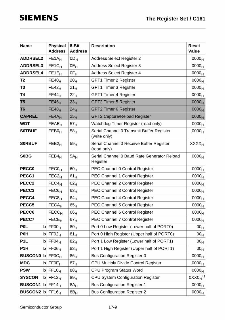
10Jul97@15:19h The Register Set / C161
ADDRSEL2 FE1AH 0DH Address Select Register 2 0000H
ADDRSEL3 FE1CH 0EH Address Select Register 3 0000H
ADDRSEL4 FE1EH 0FH Address Select Register 4 0000H
T2 FE40H 20H GPT1 Timer 2 Register 0000H
T3 FE42H 21H GPT1 Timer 3 Register 0000H
T4 FE44H 22H GPT1 Timer 4 Register 0000H
T5 FE46H 23H GPT2 Timer 5 Register 0000H
T6 FE48H 24H GPT2 Timer 6 Register 0000H
CAPREL FE4AH 25H GPT2 Capture/Reload Register 0000H
WDT FEAEH 57H Watchdog Timer Register (read only) 0000H
S0TBUF FEB0H 58H Serial Channel 0 Transmit Buffer Register(write only)
0000H
S0RBUF FEB2H 59H Serial Channel 0 Receive Buffer Register(read only)
XXXXH
S0BG FEB4H 5AH Serial Channel 0 Baud Rate Generator Reload Register
0000H
PECC0 FEC0H 60H PEC Channel 0 Control Register 0000H
PECC1 FEC2H 61H PEC Channel 1 Control Register 0000H
PECC2 FEC4H 62H PEC Channel 2 Control Register 0000H
PECC3 FEC6H 63H PEC Channel 3 Control Register 0000H
PECC4 FEC8H 64H PEC Channel 4 Control Register 0000H
PECC5 FECAH 65H PEC Channel 5 Control Register 0000H
PECC6 FECCH 66H PEC Channel 6 Control Register 0000H
PECC7 FECEH 67H PEC Channel 7 Control Register 0000H
P0L b FF00H 80H Port 0 Low Register (Lower half of PORT0) 00H
P0H b FF02H 81H Port 0 High Register (Upper half of PORT0) 00H
P1L b FF04H 82H Port 1 Low Register (Lower half of PORT1) 00H
P1H b FF06H 83H Port 1 High Register (Upper half of PORT1) 00H
BUSCON0 b FF0CH 86H Bus Configuration Register 0 0000H
MDC b FF0EH 87H CPU Multiply Divide Control Register 0000H
PSW b FF10H 88H CPU Program Status Word 0000H
SYSCON b FF12H 89H CPU System Configuration Register 0XX0H1)
BUSCON1 b FF14H 8AH Bus Configuration Register 1 0000H
BUSCON2 b FF16H 8BH Bus Configuration Register 2 0000H
Name PhysicalAddress
8-BitAddress
Description ResetValue
Semiconductor Group 17-9

10Jul97@15:19h The Register Set / C161
BUSCON3 b FF18H 8CH Bus Configuration Register 3 0000H
BUSCON4 b FF1AH 8DH Bus Configuration Register 4 0000H
ZEROS b FF1CH 8EH Constant Value 0’s Register (read only) 0000H
ONES b FF1EH 8FH Constant Value 1’s Register (read only) FFFFH
T2CON b FF40H A0H GPT1 Timer 2 Control Register 0000H
T3CON b FF42H A1H GPT1 Timer 3 Control Register 0000H
T4CON b FF44H A2H GPT1 Timer 4 Control Register 0000H
T5CON b FF46H A3H GPT2 Timer 5 Control Register 0000H
T6CON b FF48H A4H GPT2 Timer 6 Control Register 0000H
T2IC b FF60H B0H GPT1 Timer 2 Interrupt Control Register 0000H
T3IC b FF62H B1H GPT1 Timer 3 Interrupt Control Register 0000H
T4IC b FF64H B2H GPT1 Timer 4 Interrupt Control Register 0000H
T5IC b FF66H B3H GPT2 Timer 5 Interrupt Control Register 0000H
T6IC b FF68H B4H GPT2 Timer 6 Interrupt Control Register 0000H
CRIC b FF6AH B5H GPT2 CAPREL Interrupt Control Register 0000H
S0TIC b FF6CH B6H Serial Channel 0 Transmit Interrupt Control Register
0000H
S0RIC b FF6EH B7H Serial Channel 0 Receive Interrupt Control Register
0000H
S0EIC b FF70H B8H Serial Channel 0 Error Interrupt Control Register 0000H
SSCTIC b FF72H B9H SSC Transmit Interrupt Control Register 0000H
SSCRIC b FF74H BAH SSC Receive Interrupt Control Register 0000H
SSCEIC b FF76H BBH SSC Error Interrupt Control Register 0000H
CC9IC b FF8AH C5H External Interrupt 1 Control Register 0000H
CC10IC b FF8CH C6H External Interrupt 2 Control Register 0000H
CC11IC b FF8EH C7H External Interrupt 3 Control Register 0000H
CC12IC b FF90H C8H External Interrupt 4 Control Register 0000H
CC13IC b FF92H C9H External Interrupt 5 Control Register 0000H
CC14IC b FF94H CAH External Interrupt 6 Control Register 0000H
CC15IC b FF96H CBH External Interrupt 7 Control Register 0000H
P5 b FFA2H D1H Port 5 Register (read only) XXXXH
TFR b FFACH D6H Trap Flag Register 0000H
WDTCON b FFAEH D7H Watchdog Timer Control Register 000XH2)
Name PhysicalAddress
8-BitAddress
Description ResetValue
Semiconductor Group 17-10

10Jul97@15:19h The Register Set / C161
Note:1) The system configuration is selected during reset.2) Bit WDTR indicates a watchdog timer triggered reset.
S0CON b FFB0H D8H Serial Channel 0 Control Register 0000H
SSCCON b FFB2H D9H SSC Control Register 0000H
P2 b FFC0H E0H Port 2 Register 0000H
DP2 b FFC2H E1H Port 2 Direction Control Register 0000H
P3 b FFC4H E2H Port 3 Register 0000H
DP3 b FFC6H E3H Port 3 Direction Control Register 0000H
P4 b FFC8H E4H Port 4 Register (8 bits) 00H
DP4 b FFCAH E5H Port 4 Direction Control Register 00H
P6 b FFCCH E6H Port 6 Register (8 bits) 00H
DP6 b FFCEH E7H Port 6 Direction Control Register 00H
Name PhysicalAddress
8-BitAddress
Description ResetValue
The shaded registers are only available in the C161O, not in the C161V and the C161K.
Semiconductor Group 17-11
10Jul97@15:19h The Register Set / C161
17.4 Special Notes
PEC Pointer Registers
The source and destination pointers for the peripheral event controller are mapped to a special areawithin the internal RAM. Pointers that are not occupied by the PEC may therefore be used likenormal RAM. During Power Down mode or any warm reset the PEC pointers are preserved.
The PEC and its registers are described in chapter “Interrupt and Trap Functions”.
GPR Access in the ESFR Area
The locations 00’F000H...00’F01EH within the ESFR area are reserved and allow to access thecurrent register bank via short register addressing modes. The GPRs are mirrored to the ESFR areawhich allows access to the current register bank even after switching register spaces (see examplebelow).
MOV R5, DP3 ;GPR access via SFR areaEXTR #1MOV R5, ODP3 ;GPR access via ESFR area
Writing Bytes to SFRs
All special function registers may be accessed wordwise or bytewise (some of them even bitwise).Reading bytes from word SFRs is a non-critical operation. However, when writing bytes to wordSFRs the complementary byte of the respective SFR is cleared with the write operation.
Semiconductor Group 17-12
10Jul97@15:19h Instruction Set Summary / C161
18 Instruction Set Summary
This chapter briefly summarizes the C161’s instructions ordered by instruction classes. Thisprovides a basic understanding of the C161’s instruction set, the power and versatility of theinstructions and their general usage.
A detailed description of each single instruction, including its operand data type, condition flagsettings, addressing modes, length (number of bytes) and object code format is provided in the“Instruction Set Manual” for the C16x Family. This manual also provides tables ordering theinstructions according to various criteria, to allow quick references.
Summary of Instruction Classes
Grouping the various instruction into classes aids in identifying similar instructions (eg. SHR, ROR)and variations of certain instructions (eg. ADD, ADDB). This provides an easy access to thepossibilities and the power of the instructions of the C161.
Note: The used mnemonics refer to the detailled description.
Arithmetic Instructions
• Addition of two words or bytes: ADD ADDB• Addition with Carry of two words or bytes: ADDC ADDCB• Subtraction of two words or bytes: SUB SUBB• Subtraction with Carry of two words or bytes: SUBC SUBCB• 16*16 bit signed or unsigned multiplication: MUL MULU• 16/16 bit signed or unsigned division: DIV DIVU• 32/16 bit signed or unsigned division: DIVL DIVLU• 1’s complement of a word or byte: CPL CPLB• 2’s complement (negation) of a word or byte: NEG NEGB
Logical Instructions
• Bitwise ANDing of two words or bytes: AND ANDB• Bitwise ORing of two words or bytes: OR ORB• Bitwise XORing of two words or bytes: XOR XORB
Compare and Loop Control Instructions
• Comparison of two words or bytes: CMP CMPB• Comparison of two words with post-increment
by either 1 or 2: CMPI1 CMPI2• Comparison of two words with post-decrement
by either 1 or 2: CMPD1 CMPD2
Semiconductor Group 18-1

10Jul97@15:19h Instruction Set Summary / C161
Boolean Bit Manipulation Instructions
• Manipulation of a maskable bit fieldin either the high or the low byte of a word: BFLDH BFLDL
• Setting a single bit (to ‘1’): BSET• Clearing a single bit (to ‘0’): BCLR• Movement of a single bit: BMOV• Movement of a negated bit: BMOVN• ANDing of two bits: BAND• ORing of two bits: BOR• XORing of two bits: BXOR• Comparison of two bits: BCMP
Shift and Rotate Instructions
• Shifting right of a word: SHR• Shifting left of a word: SHL• Rotating right of a word: ROR• Rotating left of a word: ROL• Arithmetic shifting right of a word (sign bit shifting): ASHR
Prioritize Instruction
• Determination of the number of shift cycles requiredto normalize a word operand (floating point support): PRIOR
Data Movement Instructions
• Standard data movement of a word or byte: MOV MOVB• Data movement of a byte to a word location
with either sign or zero byte extension: MOVBS MOVBZNote: The data movement instructions can be used with a big number of different addressing
modes including indirect addressing and automatic pointer in-/decrementing.
System Stack Instructions
• Pushing of a word onto the system stack: PUSH• Popping of a word from the system stack: POP• Saving of a word on the system stack,
and then updating the old word with a new value(provided for register bank switching): SCXT
Semiconductor Group 18-2
10Jul97@15:19h Instruction Set Summary / C161
Jump Instructions
• Conditional jumping to an either absolutely,indirectly, or relatively addressed target instructionwithin the current code segment: JMPA JMPI JMPR
• Unconditional jumping to an absolutely addressedtarget instruction within any code segment: JMPS
• Conditional jumping to a relatively addressedtarget instruction within the current code segmentdepending on the state of a selectable bit: JB JNB
• Conditional jumping to a relatively addressedtarget instruction within the current code segmentdepending on the state of a selectable bitwith a post-inversion of the tested bitin case of jump taken (semaphore support): JBC JNBS
Call Instructions
• Conditional calling of an either absolutelyor indirectly addressed subroutine withinthe current code segment: CALLA CALLI
• Unconditional calling of a relatively addressedsubroutine within the current code segment: CALLR
• Unconditional calling of an absolutely addressedsubroutine within any code segment: CALLS
• Unconditional calling of an absolutely addressedsubroutine within the current code segment plusan additional pushing of a selectable register ontothe system stack: PCALL
• Unconditional branching to the interrupt ortrap vector jump table in code segment 0: TRAP
Return Instructions
• Returning from a subroutinewithin the current code segment: RET
• Returning from a subroutinewithin any code segment: RETS
• Returning from a subroutine within the currentcode segment plus an additional popping of aselectable register from the system stack: RETP
• Returning from an interrupt service routine: RETI
Semiconductor Group 18-3

10Jul97@15:19h Instruction Set Summary / C161
System Control Instructions
• Resetting the C161 via software: SRST• Entering the Idle mode: IDLE• Entering the Power Down mode: PWRDN• Servicing the Watchdog Timer: SRVWDT• Disabling the Watchdog Timer: DISWDT• Signifying the end of the initialization routine
(pulls pin RSTOUT high, and disables the effect ofany later execution of a DISWDT instruction): EINIT
Miscellaneous
• Null operation which requires 2 bytes ofstorage and the minimum time for execution: NOP
• Definition of an unseparable instruction sequence: ATOMIC• Switch ‘reg’, ‘bitoff’ and ‘bitaddr’ addressing modes
to the Extended SFR space: EXTR• Override the DPP addressing scheme
using a specific data page instead of the DPPs,and optionally switch to ESFR space: EXTP EXTPR
• Override the DPP addressing schemeusing a specific segment instead of the DPPs,and optionally switch to ESFR space: EXTS EXTSR
Note: The ATOMIC and EXT* instructions provide support for uninterruptable code sequences eg.for semaphore operations. They also support data addressing beyond the limits of thecurrent DPPs (except ATOMIC), which is advantageous for bigger memory models in highlevel languages. Refer to chapter “System Programming” for examples.
Protected Instructions
Some instructions of the C161 which are critical for the functionality of the controller areimplemented as so-called Protected Instructions. These protected instructions use the maximuminstruction format of 32 bits for decoding, while the regular instructions only use a part of it (eg. thelower 8 bits) with the other bits providing additional information like involved registers. Decoding all32 bits of a protected doubleword instruction increases the security in cases of data distortion duringinstruction fetching. Critical operations like a software reset are therefore only executed if thecomplete instruction is decoded without an error. This enhances the safety and reliability of amicrocontroller system.
Semiconductor Group 18-4

10Jul97@15:19h Device Specification / C161
19 Device Specification
The device specification describes the electrical parameters of the device. It lists DC characteristicslike input, output or supply voltages or currents, and AC characteristics like timing characteristicsand requirements.
Other than the architecture, the instruction set or the basic functions of the C161 core and itsperipherals, these DC and AC characteristics are subject to changes due to device improvementsor specific derivatives of the standard device.
Therefore these characteristics are not contained in this manual, but rather provided in a separateData Sheet, which can be updated more frequently.
Please refer to the current version of the Data Sheet for all electrical parameters.
Note: In any case the specific characteristics of a device should be verified, before a new designis started. This ensures that the used information is up to date.
The figures below show the pin diagrams of the C161. They show the location of the different supplyand IO pins. A detailed description of all the pins is also found in the respective Data Sheet.
Semiconductor Group 19-1

10Jul97@15:19h Device Specification / C161
Figure 19-1Pin Description of the C161V, P-MQFP-80 Package
Semiconductor Group 19-2

10Jul97@15:19h Device Specification / C161
Figure 19-2Pin Description of the C161K, P-MQFP-80 Package
Semiconductor Group 19-3
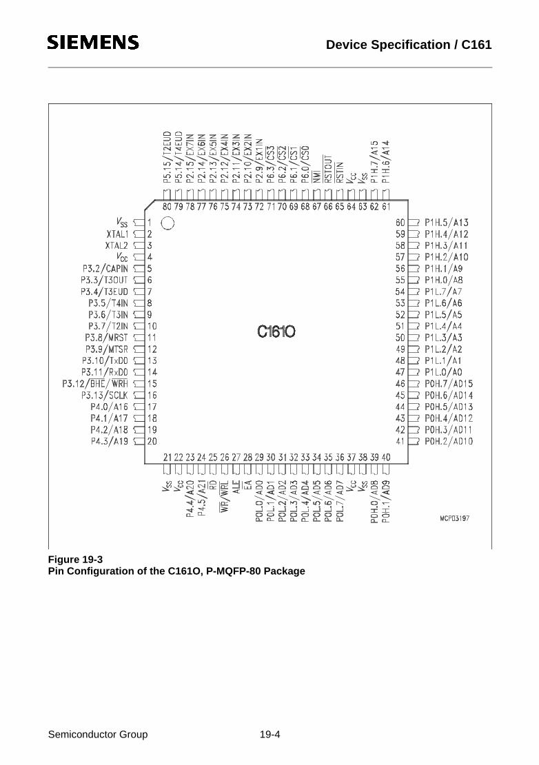
10Jul97@15:19h Device Specification / C161
Figure 19-3Pin Configuration of the C161O, P-MQFP-80 Package
Semiconductor Group 19-4
10Jul97@15:19h Keyword Index / C161
20 Keyword Index
This section lists a number of keywords which refer to specific details of the C161 in terms of itsarchitecture, its functional units or functions. This helps to quickly find the answer to specificquestions about the C161.
AAcronyms 1-6Adapt Mode 14-8Address
Arbitration 8-21Area Definition 8-20Boundaries 3-10Segment 8-8, 14-10
ADDRSELx 8-19, 8-21ALE length 8-11ALU 24Arbitration
Address 8-21ASC0
Error Detection 10-10Interrupts 10-12
ASC0, Asynchronous Serial Interface 10-1
BBaudrate
ASC0 10-10Bootstrap Loader 13-4SSC 11-10
BHE 8-7Bit
addressable memory 3-4Handling 19Manipulation Instructions 18-2protected 2-15, 19
Bootstrap Loader 13-1, 14-8Boundaries 3-10Bus
Demultiplexed 8-4Idle State 8-23Mode Configuration 8-2, 14-9Multiplexed 8-3
BUSCONx 8-17, 8-21
CCapture Mode (GPT) 9-14, 9-23CCxIC 5-22Chip Select 8-8, 14-10Clock Generator 2-9, 14-11
modes 2-9, 14-11Concatenation of Timers 9-11, 9-21Configuration
Address 8-8, 14-10Bus Mode 8-2, 14-9Chip Select 8-8, 14-10PLL 2-9, 14-11Reset 14-5Write Control 14-9
Context Switching 5-15Count direction 9-4, 9-18Counter 9-7, 9-10CP 32CPU 2-2, 11CRIC 9-26Cross Reference 1-5CSP 28
Semiconductor Group 20-1
10Jul97@15:19h Keyword Index / C161
DData Page 30, 16-13
boundaries 3-10Delay
Read/Write 8-14Demultiplexed Bus 8-4Development Support 1-5Direct Drive 2-10Direction
count 9-4, 9-18Disable
Interrupt 5-13Segmentation 23
Division 37, 16-1DP0L, DP0H 6-4DP1L, DP1H 6-7DP2 6-10DP3 6-13DP4 6-18DP6 6-23DPP 30, 16-13
EEmulation Mode 14-8Enable
Interrupt 5-13Segmentation 23
Error DetectionASC0 10-10SSC 11-12
ESFR 2-8EXICON 5-21External
Bus Characteristics 8-10 to 8-14Bus Idle State 8-23Bus Modes 8-2 to 8-7Interrupts 5-20
External Bus 2-8
FFlags 24 to 26Full Duplex 11-6
GGPR 3-6, 32, 17-2GPT 2-14GPT1 9-1GPT2 9-16
HHalf Duplex 11-8Hardware
Reset 14-1Traps 5-23
IIdle
State (Bus) 8-23Idle Mode 15-1Instruction 16-1, 18-1
Bit Manipulation 18-2Branch 14Pipeline 13protected 18-4Timing 20unseparable 16-12
InterfaceExternal Bus 8-1serial async. 10-1serial sync. 11-1
Internal RAM 3-4Interrupt
Enable/Disable 5-13External 5-20Priority 5-6Processing 5-1, 5-5Response Times 5-16Sources 5-3System 2-6, 5-2Vectors 5-3
IP 27
Semiconductor Group 20-2

10Jul97@15:19h Keyword Index / C161
MMDC 38MDH 37MDL 37Memory 2-7
bit-addressable 3-4External 3-9RAM/SFR 3-4ROM 3-3, 16-14
Memory Cycle Time 8-12Multiplexed Bus 8-3Multiplication 37, 16-1
OODP2 6-10ODP3 6-13ODP6 6-23ONES 39Open Drain Mode 6-2Oscillator
circuit 2-9
PP0L, P0H 6-4P1L, P1H 6-7P2 6-10P3 6-13P4 6-18P5 6-21P6 6-23PEC 2-7, 3-7, 5-10
Response Times 5-18PECCx 5-10Peripheral 2-11Pins 7-1, 19-2
in Idle and Power Down mode 15-5Pipeline 13
Effects 16PLL 14-11Port 2-12Power Down Mode 15-3Prescaler 2-10Protected
Bits 2-15, 19instruction 18-4
PSW 24, 5-8
RRAM
internal 3-4Read/Write Delay 8-14Register 17-1, 17-4, 17-8Reset 9-8, 14-1
Configuration 14-5Output 14-4Values 14-4
ROM 16-14RP0H 8-22
Semiconductor Group 20-3
10Jul97@15:19h Keyword Index / C161
SS0BG 10-10S0CON 10-2S0EIC, S0RIC, S0TIC, S0TBIC 10-12S0RBUF 10-7, 10-9S0TBUF 10-6, 10-9Segment
Address 8-8, 14-10boundaries 3-10
Segmentation 28Enable/Disable 23
Serial Interface 2-13, 10-1Asynchronous 10-4Synchronous 10-8, 11-1
SFR 2-8, 3-8, 17-4, 17-8Single Chip Mode 8-2Software
Reset 14-1Traps 5-23
SourceInterrupt 5-3
SP 34SSC 11-1
Baudrate generation 11-10Error Detection 11-12Full Duplex 11-6Half Duplex 11-8
SSCBR 11-10SSCCON 11-2SSCEIC, SSCRIC, SSCTIC 11-14SSCRB, SSCTB 11-7Stack 3-5, 34, 16-4Startup Configuration 14-5STKOV 35STKUN 36Subroutine 16-9Synchronous Serial Interface 11-1SYSCON 21, 22, 8-16
TT2CON 9-8T2IC, T3IC, T4IC 9-15T3CON 9-3T4CON 9-8T5CON 9-20T5IC, T6IC 9-26T6CON 9-18TFR 5-24Timer 2-14, 9-1, 9-16
Auxiliary Timer 9-8, 9-20Concatenation 9-11, 9-21Core Timer 9-3, 9-18
Tools 1-5Traps 5-4, 5-23Tri-State Time 8-13
UUnseparable instructions 16-12
WWaitstate
Memory Cycle 8-12Tri-State 8-13
Watchdog 2-14, 12-1, 14-4WDT 12-1WDTCON 12-2
XXBUS 2-9, 8-24
ZZEROS 39
Semiconductor Group 20-4