“industrial technologies for schools”...
TRANSCRIPT
IndTech 2014 for Schools CONFIDENTIAL Page 1 of 15
Industrial Technologies 2014 Conference, 09-11 April 2014, Athens, Greece
09- 11 April 2014, Athens, Greece
“Industrial Technologies for Schools”
initiative
School Name: Prototype experimental lyceum of University Patras
Title:
HIGHLY EFFICIENT ELECTRICAL ENERGY PRODUCING
NANOSTRUCTURE
Contact Persons’ Details
Name:
Surname:
Email:
Phone:
Georgios
Fyttas
+306976363296
Date 17 /03/2014

IndTech 2014 for Schools CONFIDENTIAL Page 2 of 15
Industrial Technologies 2014 Conference, 09-11 April 2014, Athens, Greece
PARTICIPANTS
Student: Name Surname
Marios-Dimitrios Karampelas
Vasiliki-Tatiani Gouda
Panagiotis Papadopoulos
Andreas Sofis
Athanasios Spetsieris
Angeliki Terpina
Theocharis Chantzis
Ioannis Avgeris
Styliani Kalyva
Kalliopi-Klelia Lykothanasi
Athina-Lydia Mageiropoulou
Dimitra Bousia
Victoria-Zoi Tsingeli
Eirini Maniatopoulou
Eleni Rousia
Ioanna-Nefeli Kokloni
Ariadni Kouzeli
Lydia Andriopoulou
Maria-Ioanna Moraiti
Responsible Teacher Name e-mail
Fyttas Georgios [email protected]
Sfaelos Ioannis [email protected]
Efstathiou Angeliki [email protected]
Tsingelis Michail [email protected]

IndTech 2014 for Schools CONFIDENTIAL Page 3 of 15
Industrial Technologies 2014 Conference
Content
PARTICIPANTS .................................................................................................................................................. 2
ABSTRACT .......................................................................................................................................................... 4
1. INTRODUCTION ....................................................................................................................................... 5
2. NEW PRODUCT / SERVICE DESCRIPTION ....................................................................................... 6
3. CONCLUSIONS ....................................................................................................................................... 13
4. APPENDIX ................................................................................. ERROR! BOOKMARK NOT DEFINED.
IndTech 2014 for Schools CONFIDENTIAL Page 4 of 15
Industrial Technologies 2014 Conference
ABSTRACT
Nowadays, the reserves of non-renewable energy are being consumed more rapidly than
ever due to the increased energy demands. As a result most of the existing energy resources
have reached the limits of exhaustion. Meanwhile, due to the air pollution caused during their
combustion, they are harming the environment, damaging the ecosystem and jeopardizing our
health. You have probably heard of the Greenhouse Effect. Effective energy conservation can
only be achieved through rational and efficient use of the existing energy reserves.
Βy saving energy, neither do we reduce, nor do we eliminate our energy demands. On the
contrary we ameliorate our living standards. Our proposal, aiming towards those directions, is
related to the application of a new “eco-friendly” method of exploitation of renewable energy
resources. Τhe photovoltaic effect, the piezoelectric effect and the superconductivity through
the use of a new ground-breaking science, nanotechnology, seem to be interesting and
financially viable and efficient solutions. Thus, we designed and “gave life” to our though by
a nanostructure that combines all these scientific effects (the photovoltaic effect, the
piezoelectric effect and the superconductivity). Our primary source of energy was solar
radiation and any form of mechanic voltage. As a result we manage to satisfy, to a great
extent the energy demands of our school (heating/air-conditioning-lighting). We encourage
the scalability and implementation of our concept and other public places.

IndTech 2014 for Schools CONFIDENTIAL Page 5 of 15
Industrial Technologies 2014 Conference
1. INTRODUCTION
Humanity is confronted to an energy source deprivation and to an extended economic
dysfunction. The energy problem in the world nowadays consists of three basic components.
As far as the environmental factor is concerned, energy production has a catastrophic impact
on nature, let alone that highly efficient forms of energy are in very short supply and their
over-exploitation destroys the local ecosystems. Furthermore, the fact that thousands of
people are added in the world population monthly makes it very likely that we are about to
face further problems in the future. Most of all, even in the western world, in countries like
ours, much of the population gets too little energy to meet the basic human needs, as they are
recreated by the technological revolution; given thatthe monetary costs of energy are rising
nearly everywhere.
This enormous reduction in the consumption of energy, in the era of economic hardships,
affects the educational process. Schools in Patras, like ours, do face a huge energy problem.
Central heating is on for a few hours in the morning, only during the unbearably cold days,
making the school environment unpleasant and unhealthy for both students and teachers.
Still, the energy consumption remains very high, forcing us to cut on further investments on
education. Plus, the unbearable heat in the early September and during the summer exams can
no way be addressed with the technological and financial means of which we dispose now, as
the installation of air conditioning systems constitutes an unattainable dream. Sadly, such
problems do not seem to be amongst the priorities, given the political and financial situation
in our country, and the fate of Greek schools remains uncertain [9].
As a society, we cannot afford to spend more money on energy, and we cannot risk
damaging the environment irreparably. It becomes our responsibility; it’s up to us, as a
student body, to come up with alternative, environmentally friendly and money saving ways
to produce our energy, contributing to the self-sufficiency of our school. So why not use all
this challenges as an inspiration? Green nanotechnology can help us reduce pollution from
energy generation and help conserve fossil fuels. Modern challenges require modern ways of
facing them. Nanotechnology is evolving constantly, getting better day by day, and will help
us reduce pollution from energy generation and conserve fossil fuels [13].
We suggest exploiting the constant movement and sound produced daily in our school,
during lessons or breaks, in the gym or in the corridors, in order to generate the energy
needed for its daily function. We imagine our school walls and floors coated by layers, which
will have the ability to convert the nanoscale mechanical energy into electrical energy by
means of piezoelectric zinc oxide nanowires, with the prospect of expanding the use of these
exagonic nanodevices outside the narrow “borders” of our school and our town.

IndTech 2014 for Schools CONFIDENTIAL Page 6 of 15
Industrial Technologies 2014 Conference
2. NEW PRODUCT / SERVICE DESCRIPTION
The origin and historical evolution of nanotechnology are unknown. The first
nanotechnologists might have been glass workers who used ovens in order to shape glass
objects.
The first scientific report on nanotechnology (without the use of that name) was in a speech
made by Richard Feynman, 1959, entitled "There's plenty of room at the bottom".
The term Nanotechnology [23], [24], [25], was first used by the Sciences University of
Tokyo professor, Norio Taniguchi in 1974 in a thesis entitled "On the concept of
Nanotechnology" to describe the precision of material manufacture with nanometer
tolerances.
Photovoltaics & Nanotechnology
The general term “photovoltaic” [7], [8], refers to the
industrial lining of more than one photovoltaic cells. In
essence it is artificial semiconductors (usually made of
silicon) which are combined in order to create an
electrical circuit in series. These semiconductors absorb
photons through solar radiation and produce an
electrical voltage [3]. This process is otherwise known
as the photovoltaic effect. The photovoltaics belong in
the category of renewable energy sources. The currently
existing photovoltaics in Greece are devised in two
generations.
Figure 1
The first generation (PV/W) of photovoltaic elements is based on the traditional technology
of silicon. On the contrary, the second generation of photovoltaic, used nowadays, mostly in
Greece, is based on the use of thin films [21]. As a result, products that belong to the second
generation are far more competitive in terms of performance. Aside from that factor, these
products possess various other important manufacturing advantages such as less material
consumption, fewer steps for completion and easier automation. Therefor, it is obvious that
photovoltaic improve thanks to the use of thinner and smaller materials, thus the creation of
the third generation photovoltaic. Third generation photovoltaic are already being used in
shelters in Los Angeles and are expected to be applied to bus stops through-out Berlin. The
special feature of this category of photovoltaic, their key difference from the other two, is that
their manufacture requires relatively low quantities of cheap materials. Goal of the
development third generation photovoltaic is a mass production of flexible photovoltaic (thin
film) with high levels of performance and various application possibilities. For the time being,
research is conduct in order to find ways to maximize the performance of such photovoltaic.
According to Dr. Constantine Fostiropoulos, a valuable advantage of third generation
photovoltaic is that they are expected to be 50% cheaper than those of the second generation
that have been launch to the market up till now. Apart from their low cost, in comparison to
the cost of silicon technology, they also offer a high level of energy automation and they are
they are more elegant in terms of appearance.
Nowadays [22], researchers are focused on increasing the levels of performance of
photovoltaic cells through the use of nanotechnology.
By using nanoparticles of germanium, silicon and other materials [11], researchers aim to
produce photovoltaic cells even more efficient, with levels of performance up to 65%.
Traditional photovoltaic cells function according to the principle: “A photon in- an electron
out.” In other words, each light particle, each photo in this case, that enters the photovoltaic

IndTech 2014 for Schools CONFIDENTIAL Page 7 of 15
Industrial Technologies 2014 Conference
cell, produces an electron and in that way we have the production of electricity that is
received as an exit.
In theory, according to this theory the maximum performance of a photovoltaic is 31%.
However, by creating photovoltaic cells from very small nanoparticles, scientists aim to
achieve a correspondence of far more than one electrons to each photon. Scientists estimate
that such a method will lead to a maximum performance that will range between 42 to 65%.
An example of combination the photovoltaic effect and nanotechnology are photovoltaic
awnings which will channel and convert the solar radiation they will absorb into other forms
of energy that are necessary for the function of various electrical appliances.
Piezoelectric Effect
The piezoelectric effect [6], [7], [12], was discovered by Pierre and Jacques Curie in 1880.
It is described in the property of certain materials (mostly crystal but some ceramic as well)
to produce electrical voltage as a result of applying certain mechanic pressure or οoscillation.
Piezoelectric can be explained qualitatively through the transportation of free charges at the
ends of a crystal mesh. Piezoelectric materials belong in the category of intelligent materials.
These materials are known for their satisfactory response to stimulus of various natures.
Generally, the piezoelectric effect is anisotropic, in other words, it appears in materials with
crystal structure without center of symmetry, and it is a first class effect [10]. In the case of
certain ceramic materials, if placed in certain temperature conditions, or else known as Curie
Temperature [2], they create inside the crystal electric dipoles of random orientation that are
macroscopically inexistent [4]. During the polarization process, in presence of a strong
electric field, these dipoles tend to form a line, leading macroscopically to the creation of an
electric dipole. After the cooling process and the removal of the polarization field, the electric
dipoles cannot return to their initial positions and the material has become permanently
piezoelectric, thus it can convert mechanic energy to electric energy and vice versa. This
property is lost only if the the temperature differs from the Curie Temperature, or if the
arrangement is submitted to a very strong electric field [2] .
Certain examples of materials with piezoelectric properties [18] are quartz (SiO2), Rochelle
salt or Seignette (tart rate, NaKC4H4O6·2H2O), the ADP (ammonium dehydrogenate
phosphate, NH4H2PO4), lithium sulfate monohydrate, (LiSO4.H2O), tourmaline, the
synthetic polymer is PVDF (polyvinylidene difluoride), etc.
Zinc oxide
Zinc oxide is an organic compound, a white
powder, which is insoluble in water. Used in
countless materials and products. As a naturally
occurring mineral, but the bulk of the produced
artificially. The crystals of occurs in three forms,
the hexagonal structure of vourtsiti (thermo-
dynamically more stable in ambient environment
and most common), the pentagonal structure of
sphalerite (stabilized if the ZnO grown on a sub-
strate lattice with cubic structure) and structure
[7] of the salt. The dominant form is hexagonal.
Figure 2

IndTech 2014 for Schools CONFIDENTIAL Page 8 of 15
Industrial Technologies 2014 Conference
The structure of wurtzite
shown in the figure 2. In an
article recently published in
Nature, scientists from the
Institute of Technology
"Georgia" developed nano-
wires of zinc oxide around
kevlar fibers.
The researchers placed the
fibers together: when the
wires rub against one ano-
Figure 3
ther, creating an electric charge, whose motion is produced in the output stream.
The ZnO has applications to piezo-electricity [8]. The piezoelectric proper-ties due to
tetrahedral crystalline structure, in which the ties between individuals are very strong. Given
the lack of central symmetry which characterizes, the center of which is composed of positive
and negative charges, may be moved due to external pressure, which will induce a field
distortion. This shift has resulted local dipole moments, so a macroscopic dipole moment
occurs in the crystal. Among the tetrahedral crystal, the ZnO has the highest piezoelectric
vector that provides high electromechanical coupling.
The piezoelectric property of ZnO nano-structures has yet to be investigated for a beneficial
applications of nanoelectro-mechanic systems. Moreover, the structures of ZnO have results
and creating nano-rings and nano-coils.
Superconductivity
Superconductivity is the state in which a material (usually metal and ceramic) have zero
ohmic resistance. Materials that are insulators have high resistance, while materials that are
conductors have little resistance [25]. These materials are called superconductors. In a
superconductor collisions between electrons and atoms are minimized with the result that
electric current flows unaffected and without any difficulty. The temperature below which a
material is called the critical temperature superconductor. For most metals the critical
temperature is close to absolute zero. So far there has been superconductor at room
temperature, a discovery that probably would have dire consequences in the technology
industry.
Interpretation
Superconductivity is considered a quantum phenomenon and rarely explained by classical
physics. Electrons are the natural hosts of the electric current in the conductors and the
scattering in the crystal lattice (and generally the material) of the conduit, during the forced
passage through it, causing the brakes and thus appears ohmic resistance [30]. The scattering
of electrons are on the atoms of the crystal:
a) due to the lattice defects (impurities, gridded spaces) that deform the crystal, and
b) due to the non-zero temperature of the crystal from which his men oscillate and occupy
larger space statistics and thus shortens the free ( by scattering ) parking pass for electrons .
IndTech 2014 for Schools CONFIDENTIAL Page 9 of 15
Industrial Technologies 2014 Conference
In terms of superconductivity things work differently. Individuals in the crystal principle no
longer oscillate strongly due to the low temperature and the grid gaps are closing. But it is not
a necessary and sufficient condition for this appearance of superconductivity.
There are several mechanisms, depending on the material, giving superconducting
properties in combination lattice - electron.
Properties of superconducting materials
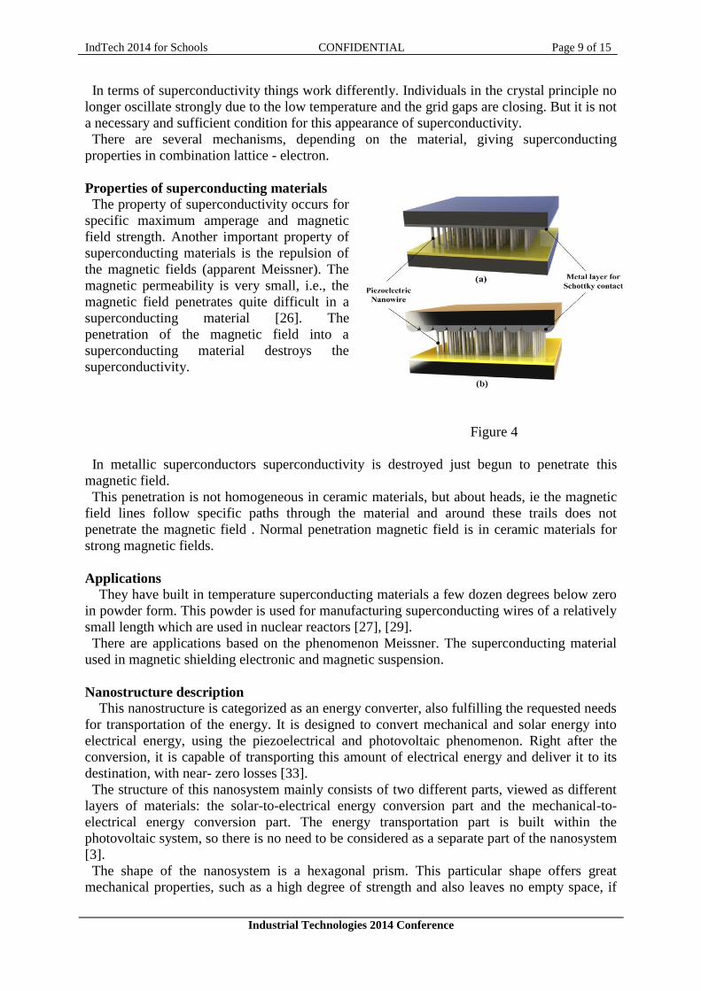
The property of superconductivity occurs for
specific maximum amperage and magnetic
field strength. Another important property of
superconducting materials is the repulsion of
the magnetic fields (apparent Meissner). The
magnetic permeability is very small, i.e., the
magnetic field penetrates quite difficult in a
superconducting material [26]. The
penetration of the magnetic field into a
superconducting material destroys the
superconductivity.
Figure 4
In metallic superconductors superconductivity is destroyed just begun to penetrate this
magnetic field.
This penetration is not homogeneous in ceramic materials, but about heads, ie the magnetic
field lines follow specific paths through the material and around these trails does not
penetrate the magnetic field . Normal penetration magnetic field is in ceramic materials for
strong magnetic fields.
Applications
They have built in temperature superconducting materials a few dozen degrees below zero
in powder form. This powder is used for manufacturing superconducting wires of a relatively
small length which are used in nuclear reactors [27], [29].
There are applications based on the phenomenon Meissner. The superconducting material
used in magnetic shielding electronic and magnetic suspension.
Nanostructure description
This nanostructure is categorized as an energy converter, also fulfilling the requested needs
for transportation of the energy. It is designed to convert mechanical and solar energy into
electrical energy, using the piezoelectrical and photovoltaic phenomenon. Right after the
conversion, it is capable of transporting this amount of electrical energy and deliver it to its
destination, with near- zero losses [33].
The structure of this nanosystem mainly consists of two different parts, viewed as different
layers of materials: the solar-to-electrical energy conversion part and the mechanical-to-
electrical energy conversion part. The energy transportation part is built within the
photovoltaic system, so there is no need to be considered as a separate part of the nanosystem
[3].
The shape of the nanosystem is a hexagonal prism. This particular shape offers great
mechanical properties, such as a high degree of strength and also leaves no empty space, if

IndTech 2014 for Schools CONFIDENTIAL Page 10 of 15
Industrial Technologies 2014 Conference
the units are placed side by side (as each side of the hexagon is touching another hexagon’s
side, six units are attached to each particular unit). The length and the distance between the
sides of the prism does not need to be defined exactly, as it varies according to the needs of
the client.
Figure 5
The first part of the nanosystem (the photovoltaic and energy transportation system) is
located on the surface layer of the nanostructure and consists of a superconducting,
photovoltaic polymer. This material is designed, not only to convert the solar energy into
electrical power, but also to transport it with minimal resistance. By the time that solar rays
are absorbed by this material, electric current starts passing through the superconductor,
being transported to the full length of the surface of the nanostructure and to other similar
nano units as well (as they are in contact, as mentioned before). Needless to mention, the
superconductor presents a high “critical temperature” , and does not need to be hypercooled
in order to gain its superconducting properties. Also standard methods of photovoltaic cells
manufacturing are followed, in order to create the necessary p-n junction – small amounts of
other materials mix with the main photovoltaic material to create a “p” and an “n” material,
and a thin “contact line” to separate them is created [1].
The second part lies deeper, within the second layer and consists the main and most
important part of the nanosystem, its core. Here, the material used is a piezoelectric, crystal –
type material. It plays its role as a “filling”, as it fills up the empty space inside the
nanostructure. In order to produce electrical power, the piezoelectric material needs to receive
waves of mechanical energy. Consequently, when a wave of this type hits the surface of the
nanostructure, it travels through the first layer until reaching the piezoelectrical filling. When
it reaches it, the wave’s mechanical energy converts into electrical power, which is
transported to the surface, where the superconductor takes care of the efficient delivery of the
energy [32].
After the electrical energy production, the produced power will be used instantly, stored or
transferred directly to the general power network.
Industrially, this nanostructure will be manufactured as a coating powder, as a textile, or
inside a liquid solution [4].
These are the default, standard and absolutely basic options of the specific product. The
nanostructure is designed so it can be improved, by using “add-on” modules or chemical
substances. This is a great advantage, so we can develop different versions of the very same
nanostructure, so it can accomplish its task under different conditions. So the possible
applications of the nanosystem are practically infinite.
Main upgrade: the Main Upgrade is the process where the majority of produced units will
be enriched with a number of substances that will protect the nanosystem from environmental

IndTech 2014 for Schools CONFIDENTIAL Page 11 of 15
Industrial Technologies 2014 Conference
factors, such as water, UV rays, toxic agents, etc. It is considered as a basic process and it is
strongly recommended for every client that uses the nanosystem. The Main Upgrade will also
prevent any unwanted process from taking place and at the same time, it will protect the
environment and the human societies. The Main Upgrade is executed by the manufacturer
and industrial producer of the nanosystem [14], [15], [16], [17].
POSSIBLE APPLICATIONS: The nanosystem is designed in such an innovative way, in
order to be able to fit theoretically everywhere. An, add-on hardened, nanostructure with the
capability to produce energy out of “nothing” and able to replace older power networks with
low cost and efficiency, is a really attracting idea with nearly countless applications [19]. The
general idea is based on a specific logic: if you apply mechanical pressure on a surface coated
with the nanosystem, which can absorb solar rays at the same time, you are producing
electrical power. An example application of the nanosystem is the school building: external
walls, internal walls, corridors, staircases and classrooms are the recommended locations for
coating, because maximum mechanical pressure and solar radiation is expected [5].
Also, the nanostructure will be used as the main construction material for the power
transportation network, replacing older, conventional systems.
Some other applications are displayed below:
Aerospace: the nanosystem will be used as a covering material on aircrafts’ wings, fuselage,
and other external parts. Air’s pressure on these surfaces and the absorption of solar rays will
lead the nanosystem to produce electrical power. The same basis will be used on space
rockets and satellites (especially in satellites, as the nanostructure will allow the
transformation of solar energy into electrical power without the need to use solar wings and
as a result, cost will be reduced). The electrical energy produced will be used to power
several subsystems of these machines [28]. Add-ons can be used to give the nanostructure
additional capabilities, such as thermal shielding, ballistic protection, EM protection,
radioactive protection, etc.
Civil Engineering: in this sector, the nanosystem will be used along with add-ons, in order to
present structural stability and strength against environmental factors, so that it can be used in
buildings, bridges, roads, rail tracks, and other similar structures. It will provide these
structures with the capability to transform considerable amounts of energy 24 hours per day,
as even the smallest ground movement will be exploited by the nanosystem to produce
energy. This also means that human movement on these surfaces will produce energy. Also,
the nanosystem will be producing electrical energy all-day long, by absorbing solar rays.
Standard electrical installations will be considered useless too, as the nanostructure will
transport the electrical power where it is needed. Moreover other systems will be replaced by
the nanosystem, for example, standard public lighting will be replaced by fluorescent
nanosystems [20].
Electronics: TVs, smartphones, computers, and generally, modern electronic devices, require
important amounts of energy to work properly. As a result, autonomous charging would be a
great feature for them. Here the nanosystem will be mainly used as the primary construction
material of these devices. The longer their daily users use them, the greater the amount of
energy produced. A smartphone is a representative example of this “use & charge” logic [31].

IndTech 2014 for Schools CONFIDENTIAL Page 12 of 15
Industrial Technologies 2014 Conference
Railways & Automobile: External surfaces, internal surfaces, mechanical parts, and all other
locations of these vehicles where mechanical pressure and solar rays are expected, will be
coated with the nanosystem, in order to produce the highest amount of energy possible.
Shipbuilding: ships’ and submarines’ external surfaces and other parts of the ship, like the
living quarters, (where movement and solar rays are expected), will be coated with the
nanosystem.
Energy producing facilities: hydroelectric plants, solar energy facilities, wind turbines and
coastal wave powerhouses are some excellent places of application of the nanostructure, as, if
used, it will act as an auxiliary, power loss – preventive, energy producer.
Clothing and shoes: the nanosystem is built-in the clothing apparel, in the form of textile.
Energy is produced with every single move of the body and also, walking is now transformed
into a standard, reliable way of energy production for the satisfaction of instant needs (the
charging of a cell phone for example).

IndTech 2014 for Schools CONFIDENTIAL Page 13 of 15
Industrial Technologies 2014 Conference
3. CONCLUSIONS
Nanotechnology is, with no doubt, a vast scientific field that has developed swiftly. It
seems as if the future of nanotechnology resembles to a certain sort of science fiction. In
terms of energy production, nanotechnology can be applied in various ways.
Through the description of the nanostructure depicted above we attempted to focus on the
photovoltaic effect, the exploitation of the piezoelectric effect and superconductivity.
Inspired by the current hearting problems in our school community, we designed and
produced our own nanoproduct.. After coating each and every surface of both the interior and
the exterior of the building, our school is now functioning on environmentaly friendly,
atternative energy which we produce on our own.
Apart from solving all the economic difficulties we faced, we do feel active citizens and part
of the contemporary eco-movement, contributing to the preservation and the well-being of
the local and global climate.
We do hope that our achievement is accepted in the global community.
The mass production of this design will not solve the global energy problems, but it will be
the ultimate low-cost proposal for a “greener” and efficient electrical energy production. As a
result, future needs on the production and the transportation of the electrical power will be
more easily fulfilled.
We assess that the evolution of new innovative and revolutionary sciences and technologies,
such as nanotechnology, can offer opportunities in term of financial improvement, the
creation of new industries two things that are vital to our country, especially these difficult
times of recession. It appears that traditional industries are becoming fewer and fewer and
international. As a result the exploitation of nanotechnology through entrepreneurial activity
could be an opportunity for the Greek economy.

IndTech 2014 for Schools CONFIDENTIAL Page 14 of 15
Industrial Technologies 2014 Conference
4. REFERENCES
Books References Examples
[1] Simchi-Levi D, 2010, Operation Rules, MIT Press Ltd.
[2] Shapiro J, 2001, Modelling the Supply Chain, Duxbury, Thomson Learning Inc.
[3] R.Serway, 1990, ”PHYSICS FOR SCIENTISTS & ENGINEERS (WITH MODERN
PHYSICS), Third Edition, Saunders Golden Sunburst Series, Saunders College
Publishing.
[4] D.Ebbing – S.Gammon,2002 General Chemistry 6th Edition Houghton Mifflin Company
Shapiro J, 2001, Modelling the Supply Chain, Duxbury, Thomson Learning Inc.
[5] D. Driankov, H. Hellendoorn, M. Reinfrak, An introduction to fuzzy control. 2nd edition,
Springer Verlag, 1996.
[6] A. Preumont, Mechatronics. Dynamics of electromechanical and piezoelectricsystems,
ULB Active Structures Laboratory, Brussels, Belgium, Springer 2006.
[7] Cutillo M. Photoelectrochemical Cells : The Energy Source of the Future.
University of Pennsylvania, Philadelphia, 2007.
[8] Hagfeldt A, Didriksson B, Palmqvist T, Lindström H, Södergren S, Rensmo H,
Lindquist S.E. Solar Energy Materials & Solar Cells. 1994, Τομ. 31, σσ. 481-488.
Journal References Examples
[9] Mourtzis D, Doukas M, Psarommatis F, 2012, A multi-criteria evaluation of centralized
and decentralized production networks in a highly customer-driven environment. CIRP
Annals – Manufacturing Technology, 61/1:427-430.
[10] Zhou G, Min H, Gen M, 2002, The balanced allocation of customers to multiple
distribution centers in the supply chain network: a genetic algorithm approach, Computers &
Industrial Engineering, 43/1–2:251–261.
[11] Dawson T, Nanomaterials for textile processing and photonic applications,
Coloration Technology,Volume 124, Issue 5, pages 261–272, October 2008.
[12] H. Irschik, A review of static and dynamic shape control of structures
usingpiezoelectric actuation. Engineering Structures, 24(1), 5-11, 2002.
[13] D.G. Marinova, G.E. Stavroulakis, E.C. Zacharenakis, Robust control of smartbeams in
the presence of damage-induced structural uncertainties. International Conference
PhysCon 2005 August 24-26, 2005, Saint Petersburg, Russia.
[14] G.E. Stavroulakis, G.A. Foutsitzi, E.P. Hadjigeoriou, D.G. Marinova, E.C.Zacharenakis,
C.C. Baniotopoulos, Numerical experiments on smart beams andplates.
[15] B. Miara, G.E. Stavroulakis, V. Valente, eds. Topics on Mathematics for Smart Systems,
European Conference, Roma, 26-28 October 2006, 218-236, World Scientific Publishers,
2007.
[16] Y. Marinakis, M. Marinaki, G.E. Stavroulakis, Particle Swarm Optimization Approach
for Structural Control. 6th GRACM International Congress on Computational
Mechanics, Thessaloniki, 19-21 June 2008.
[17] G. Foutsitzi, E. Hadjigeorgiou, D. Marinova, G. Stavroulakis, Analysis and control of
smart viscoelastic beams, 5th GRACM International Congress on Computational
Mechanics Limassol, 29 June – 1 July 2005.

IndTech 2014 for Schools CONFIDENTIAL Page 15 of 15
Industrial Technologies 2014 Conference
[18] G. Foutsitzi, D. Marinova, G. Stavroulakis, E. Hadjigeorgiou,Vibration controlanalysis
of smart piezoelectric composite plates, 2nd International Conference“From Scientific
Computing to Computational Engineering” 2nd IC-SCCE,Athens, 5-8 July, 2006.
[19] Sass J, Nanotechnology’s Invisible Threat, NRDC Issue Paper, May 2007.
[20] Wang P, Klein C, Humphry-Baker R, Zakeeruddin S.M., Grätzel M. Applied Physics
Letters. 2005, Τομ. 86 (123508).
[21] Krašovec U, Berginc M, Hočevar M, Topič M. Solar Energy Materials & Solar Cells.
2009, Τομ. 93, σσ. 379 – 381.
[22] Beyer W, Hüpkes J, Stiebig H. Thin Solid Films. 2007, Τομ. 516, σσ. 147 – 154.
Websites Reference Examples
[23] EPA, 2010, URL: www.epa.gov.
[24] http://www.gla.ac.uk/services/rande/pub/defence/newsevents/composite_materials pre-
sentations/glasgowcomp071.pdf Pethrick R, Nanomaterials for Composites, University
of Strathclyde, Scotland.
[25] www.wikipedia.com
[26] http://www.laser-applications.eu/attachments/File/FilmSolar/27-9_poster 2013.pdf
[27] http://www.nano.gr/nanotechnology_detail.asp?iArt=324&iType=74
[28] http://www.laser-applications.eu/attachments/File/FilmSolar/27-9_poster_2013.pdf
[29] http://www.econews.gr/
[30] http://technolnews.blogspot.gr/ [31] http://www.innovation.gov.au/Industry/Nanotechnology/NationalEnablingTechnologies
Strategy/Pages/NETSPublications.aspx
[32] http://www.innovation.gov.au/INDUSTRY/NANOTECHNOLOGY/Pages/default.aspx
]33] www.fas.com