independent operation of parallel three-phase converters ... · pdf fileindependent operation...
TRANSCRIPT
Independent Operation of Parallel Three-Phase
Converters for Motor Drive Applications
by
W. Daniel Fingas
A thesis submitted in conformity with the requirementsfor the degree of Masters of Applied Science
Graduate Department of Electrical and Computer Engineering
University of Toronto
Copyright c© 2009 by W. Daniel Fingas

Abstract
Independent Operation of Parallel Three-Phase Converters for Motor Drive
Applications
W. Daniel Fingas
Masters of Applied Science
Graduate Department of Electrical and Computer Engineering
University of Toronto
2009
A motor drive consisting of two parallel voltage-sourced converters was developed and
implemented. A parallel converter arrangement allows the system to be constructed in a
modular fashion to gain economies of scale and redundancy. The converters are connected
to common ac- and dc-buses without isolation and are controlled without inter-converter
communication or a master/slave arrangement. The system was simulated and the results
validated against an experimental setup. Both steady-state and dynamic load sharing
were achieved through the use of drooped PI speed regulators. PI controllers were used
to regulate the quadrature currents provided by each converter. Circulating 0-sequence
current was regulated using P controllers. A linearized state-space model of the system
was developed and an eigenvalue analysis was performed, showing system stability. Speed
steps in simulation and in the laboratory demonstrated good response. The loss of one
converter’s gating was emulated. The system continued to operate, showing an advantage
of system redundancy.
ii

Acknowledgements
I would like to thank Professor Peter Lehn for his guidance and patience even through late
nights in the laboratory! His wisdom and approachability were very much appreciated.
Professor Francis Dawson and Jack Goldstein were also always willing to offer assis-
tance.
I would also like to acknowledge and express thanks for the financial support of
the people of Canada, provided through the Natural Sciences and Engineering Research
Council of Canada (NSERC) in the form of a postgraduate scholarship for one year during
the course of my research.
I also thank God for blessing me with this opportunity to learn in such a supportive
and challenging environment.
iii

Contents
1 Introduction 1
1.1 Motivation . . . . . . . . . . . . . . . . . . . . . . . . . . . . . . . . . . . 1
1.2 Project Objectives . . . . . . . . . . . . . . . . . . . . . . . . . . . . . . 2
1.3 Literature Review . . . . . . . . . . . . . . . . . . . . . . . . . . . . . . . 2
1.3.1 Load Sharing . . . . . . . . . . . . . . . . . . . . . . . . . . . . . 3
1.3.2 0-Sequence Circulating Current . . . . . . . . . . . . . . . . . . . 4
1.4 Overview of Thesis . . . . . . . . . . . . . . . . . . . . . . . . . . . . . . 5
2 System Description 6
2.1 Overview . . . . . . . . . . . . . . . . . . . . . . . . . . . . . . . . . . . . 6
2.2 Permanent-Magnet Synchronous Machine . . . . . . . . . . . . . . . . . . 7
2.2.1 Machine Description . . . . . . . . . . . . . . . . . . . . . . . . . 7
2.2.2 Machine Loading . . . . . . . . . . . . . . . . . . . . . . . . . . . 9
2.3 Converters and Control Hardware . . . . . . . . . . . . . . . . . . . . . . 10
2.3.1 Converter and Cdc . . . . . . . . . . . . . . . . . . . . . . . . . . 10
2.3.2 RT-Linux Controllers . . . . . . . . . . . . . . . . . . . . . . . . . 10
2.3.3 Anti-Aliasing Filters . . . . . . . . . . . . . . . . . . . . . . . . . 10
2.4 dc Side . . . . . . . . . . . . . . . . . . . . . . . . . . . . . . . . . . . . . 11
2.4.1 dc Source . . . . . . . . . . . . . . . . . . . . . . . . . . . . . . . 11
2.4.2 dc Chokes Ldc . . . . . . . . . . . . . . . . . . . . . . . . . . . . . 12
iv

2.5 ac Filters . . . . . . . . . . . . . . . . . . . . . . . . . . . . . . . . . . . 12
2.5.1 Filter Description . . . . . . . . . . . . . . . . . . . . . . . . . . . 12
2.5.2 Implementation Details . . . . . . . . . . . . . . . . . . . . . . . . 13
2.5.3 Switching Ripple in the Two-VSC Configuration . . . . . . . . . . 14
2.5.4 Characterization of 0-Sequence Switching Ripple . . . . . . . . . . 16
2.6 Chapter Conclusion . . . . . . . . . . . . . . . . . . . . . . . . . . . . . . 18
3 System Model 22
3.1 Overview . . . . . . . . . . . . . . . . . . . . . . . . . . . . . . . . . . . . 22
3.2 Machine Model . . . . . . . . . . . . . . . . . . . . . . . . . . . . . . . . 22
3.2.1 Rotating qd0 Reference Frame . . . . . . . . . . . . . . . . . . . . 23
3.2.2 Machine Equations . . . . . . . . . . . . . . . . . . . . . . . . . . 24
3.2.3 Input-Output Block for Machine Equations . . . . . . . . . . . . . 26
3.3 Averaged Converter Circuit . . . . . . . . . . . . . . . . . . . . . . . . . 27
3.3.1 qd Averaged Model . . . . . . . . . . . . . . . . . . . . . . . . . . 28
3.3.2 0-Sequence Averaged Model . . . . . . . . . . . . . . . . . . . . . 29
3.4 qd Model of the Parallel Converter Arrangement . . . . . . . . . . . . . . 30
3.4.1 qd State-Space Derivation . . . . . . . . . . . . . . . . . . . . . . 30
3.5 0-Sequence Model of the Parallel Converter
Arrangement . . . . . . . . . . . . . . . . . . . . . . . . . . . . . . . . . 34
3.6 Complete Two-VSC System . . . . . . . . . . . . . . . . . . . . . . . . . 35
3.6.1 Control Considerations for the Two-Converter System . . . . . . . 35
4 Controller Development 37
4.1 Control Methodology . . . . . . . . . . . . . . . . . . . . . . . . . . . . . 37
4.2 0-Sequence Control . . . . . . . . . . . . . . . . . . . . . . . . . . . . . . 38
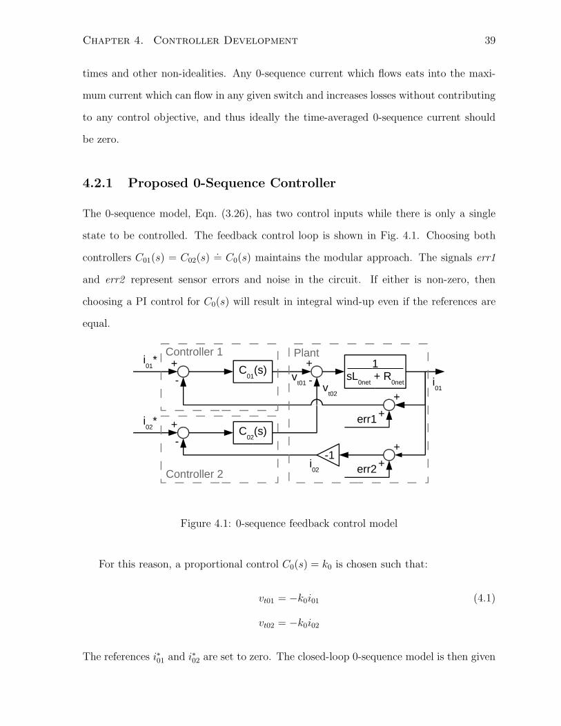
4.2.1 Proposed 0-Sequence Controller . . . . . . . . . . . . . . . . . . . 39
4.3 Machine Control . . . . . . . . . . . . . . . . . . . . . . . . . . . . . . . 40
v
4.3.1 Conventional Single Converter Field-Oriented Control . . . . . . . 40
4.3.2 Extension to the Two-Converter Case . . . . . . . . . . . . . . . . 41
4.4 Closed-Loop Two-Converter System Model . . . . . . . . . . . . . . . . . 43
4.4.1 Speed Control Loop . . . . . . . . . . . . . . . . . . . . . . . . . . 44
4.4.2 q-axis Control Loop . . . . . . . . . . . . . . . . . . . . . . . . . . 44
4.4.3 d -axis Control Loop . . . . . . . . . . . . . . . . . . . . . . . . . 45
4.4.4 Closed-Loop Model . . . . . . . . . . . . . . . . . . . . . . . . . . 46
4.5 Stability Analysis . . . . . . . . . . . . . . . . . . . . . . . . . . . . . . . 51
4.5.1 Common- and Differential-Mode Currents . . . . . . . . . . . . . 51
4.5.2 Lunze Transform . . . . . . . . . . . . . . . . . . . . . . . . . . . 52
4.5.3 Common- and Differential-Mode System Model . . . . . . . . . . 54
4.5.4 Eigenvalue Analysis . . . . . . . . . . . . . . . . . . . . . . . . . . 55
5 Results 59
5.1 Overview . . . . . . . . . . . . . . . . . . . . . . . . . . . . . . . . . . . . 59
5.2 Machine Model Validation . . . . . . . . . . . . . . . . . . . . . . . . . . 59
5.2.1 Open-Loop Response . . . . . . . . . . . . . . . . . . . . . . . . . 59
5.2.2 Closed-Loop Response . . . . . . . . . . . . . . . . . . . . . . . . 63
5.3 System Response to Speed Steps . . . . . . . . . . . . . . . . . . . . . . 65
5.3.1 Low Speed Test . . . . . . . . . . . . . . . . . . . . . . . . . . . . 65
5.3.2 High Speed Test . . . . . . . . . . . . . . . . . . . . . . . . . . . 71
5.4 Loss of Converter . . . . . . . . . . . . . . . . . . . . . . . . . . . . . . . 76
6 Conclusions 79
A Motor Details 84
B Implementation Issues 89
B.1 Common-Mode Signal Filters . . . . . . . . . . . . . . . . . . . . . . . . 89
vi

B.2 Simulation Stability . . . . . . . . . . . . . . . . . . . . . . . . . . . . . . 90
B.3 Time-Step Size and Solver Choice . . . . . . . . . . . . . . . . . . . . . . 90
C RT-Linux Control Code 91
D Description of RT-Linux Interface 108
vii

List of Tables
2.1 System Parameters . . . . . . . . . . . . . . . . . . . . . . . . . . . . . . 7
2.2 Motor Parameters . . . . . . . . . . . . . . . . . . . . . . . . . . . . . . . 9
4.1 Controller gains and operating points . . . . . . . . . . . . . . . . . . . . 56
A.1 10-pin encoder pinout . . . . . . . . . . . . . . . . . . . . . . . . . . . . . 86
viii

List of Figures
2.1 System Schematic . . . . . . . . . . . . . . . . . . . . . . . . . . . . . . . 8
2.2 Screenshot of the control interface. . . . . . . . . . . . . . . . . . . . . . 11
2.3 One of the two common-mode chokes constructed for this project. . . . . 14
2.4 Closed-loop path for the 0-sequence switching ripple current. . . . . . . . 16
2.5 Explanation of duty cycles for a requested voltage of 0.10 p.u.: (a) Con-
verter 1’s voltage references, highlighting the time period examined in
(b)-(d). (b) Requested voltages (normalized against the dc supply voltage
vtabc1
vDC/2) and the triangular carrier signal (c) Duty cycles resulting from the
comparison and (d) Instantaneous vqd0 for converter 1. . . . . . . . . . . 19
2.6 The (a) minimum and (b) maximum 0-sequence driving voltage when two
asynchronous converters are present, corresponding to the region around
in-phase and 180 out-of-phase switching, respectively. As in Fig. 2.5, the
requested voltage was 0.10 p.u. . . . . . . . . . . . . . . . . . . . . . . . 20
2.7 Experimentally observed 0-sequence ripple current, 6.7 A/V (i.e. 0.67 A/-
div). (a) Minimum ripple, corresponding to the converters near in-phase
and (b) maximum ripple, when the converters are switching 180 out-of-
phase. . . . . . . . . . . . . . . . . . . . . . . . . . . . . . . . . . . . . . 21
3.1 Alignment of the Reference-Frame with respect to the Rotor Magnet . . 24
3.2 The qd0 motor block. . . . . . . . . . . . . . . . . . . . . . . . . . . . . . 26
3.3 The separate (a) qd and (b) 0-sequence motor input/output blocks. . . . 27
ix
3.4 A single converter with its input and output filters . . . . . . . . . . . . 28
3.5 Averaged qd model for a single converter. . . . . . . . . . . . . . . . . . . 28
3.6 Averaged qd model for the two-converter system . . . . . . . . . . . . . . 29
3.7 Averaged model of the 0-sequence circuit. . . . . . . . . . . . . . . . . . 29
4.1 0-sequence feedback control model . . . . . . . . . . . . . . . . . . . . . . 39
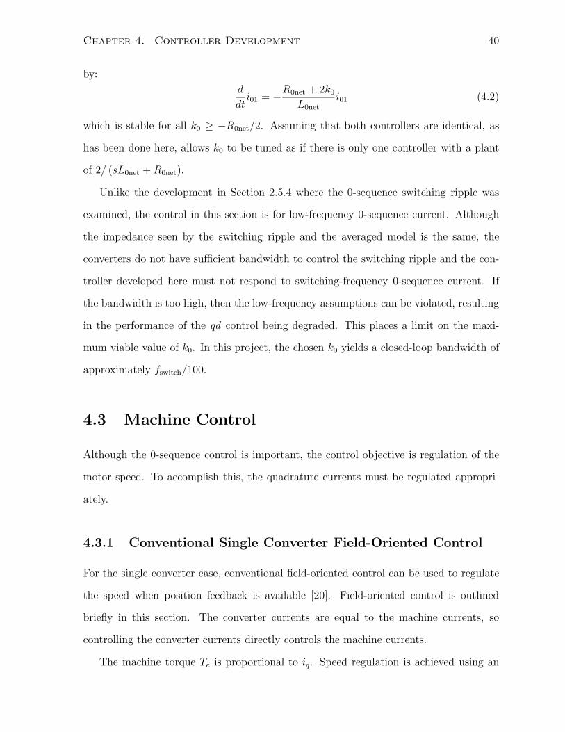
4.2 Conventional single-converter field-oriented control loop . . . . . . . . . . 41
4.3 Field-oriented control loop extended for the parallel converter system . . 43
4.4 Overall controller flow diagram . . . . . . . . . . . . . . . . . . . . . . . 47
4.5 Common-Mode Eigenvalues . . . . . . . . . . . . . . . . . . . . . . . . . 57
4.6 Differential-Mode Eigenvalues . . . . . . . . . . . . . . . . . . . . . . . . 58
5.1 (a) Simulation and (b) experimental results for vq step from 15 to 20 V .
ωe is [20 rad/s/div] and iq and id are [5 A/div]. Experimental time is in ms. 61
5.2 (a) Simulation and (b) experimental results for a 5 V step in vd. ωe is
[20 rad/s/div] and iq and id are [10 A/div]. Experimental time is in ms. . 62
5.3 (a) Simulation and (b) experimental results for iqref step from 0.74 to 15.94
A. ωe is [20 rad/s/div] and iq and id are [5 A/div]. Experimental time is
in ms. . . . . . . . . . . . . . . . . . . . . . . . . . . . . . . . . . . . . . 64
5.4 Experimental: Response of VSC1 & VSC2 to a step in speed reference at
t = 0.0 s from 62 to 124 rad/s (electrical). . . . . . . . . . . . . . . . . . 67
5.5 Experimental: Difference in Response Between VSC1 & VSC2 to a step
in speed reference at t = 0.0 s from 62 to 124 rad/s (electrical). . . . . . 68
5.6 Simulation: Response of VSC1 & VSC2 to a step in speed reference at
t = 0.1 s from 62 to 124 rad/s (electrical). . . . . . . . . . . . . . . . . . 69
5.7 Simulation: Difference in Response Between VSC1 & VSC2 to a step in
speed reference at t = 0.1 s from 62 to 124 rad/s (electrical). . . . . . . . 70
x
5.8 Experimental: Response of VSC1 & VSC2 to a step in speed reference at
t = 0.0 s from 356 to 419 rad/s (electrical). . . . . . . . . . . . . . . . . . 72
5.9 Experimental: Difference in Response Between VSC1 & VSC2 to a step
in speed reference at t = 0.0 s from 356 to 419 rad/s (electrical). . . . . . 73
5.10 Simulation: Response of VSC1 & VSC2 to a step in speed reference at
t = 0.1 s from 356 to 419 rad/s (electrical). . . . . . . . . . . . . . . . . . 74
5.11 Simulation: Difference in Response Between VSC1 & VSC2 to a step in
speed reference at t = 0.1 s from 356 to 419 rad/s (electrical). . . . . . . 75
5.12 Experimental test of the loss of gating signals for converter 2: from steady-
state, at t = 0.2 seconds. Shown are the speed and qd0 currents for both
converters. . . . . . . . . . . . . . . . . . . . . . . . . . . . . . . . . . . . 77
5.13 Simulation of the loss of gating signals for converter 2: from steady-state,
at t = 0.2 seconds. Shown are the speed and qd0 currents for both converters. 78
A.1 Motor Information for Kollmorgen Goldline M-803-A. . . . . . . . . . . . 88
D.1 Screenshot of the Control Interface . . . . . . . . . . . . . . . . . . . . . 108
xi

Chapter 1
Introduction
1.1 Motivation
Power electronic converters have increasingly been used in motor drive applications.
These converters provide increased flexibility by allowing for low-speed, high-torque op-
eration while still maintaining high efficiency and limiting the peak current. Conventional
motor drives consist of a single controller which controls one or more three-phase dc-ac
voltage-sourced converter (VSC) modules, where the number of modules required is a
function of the power rating and module size.
A parallel arrangement of VSCs making use of autonomous controllers is proposed for
motor drive applications. In this configuration, two or more converters will drive a single
motor load. The two main advantages of this setup are modularity and redundancy.
For modularity, a larger converter can be constructed from several smaller converters,
each with separate control. As each controller/converter block pair is independent, they
can be designed as modular elements and as a result benefit from economies of scale.
Due to the independent converter blocks, (n + 1) redundancy can easily be achieved by
providing one more converter than is required for a given power rating. Because both the
controller and converter are redundant, the converters do not introduce a single point of
1
Chapter 1. Introduction 2
failure.
To realize cost savings associated with parallel converters it is essential to limit ad-
ditional hardware, such as bulky isolation transformers. For this reason, a configuration
with directly-connected ac- and dc-buses is chosen.
1.2 Project Objectives
The objective of this thesis is to determine the feasibility of constructing an independently
controlled parallel-VSC arrangement. To do this, the simplest characteristic parallel
motor drive, consisting of two converters, is examined.
The project consists of the mathematical derivation of the system model, develop-
ment of an appropriate controller, and validation through simulation and experiment.
A linearized small-signal state-space model of the system and controller is developed in
order to achieve system stability. The system is simulated in MATLAB/Simulink and
the results are validated against an experimental system which was developed for this
project.
Two main problems were encountered: load sharing (both dynamic and steady-state)
and circulating 0-sequence current. The literature survey, presented in the next section,
introduces the existing research on these two issues.
1.3 Literature Review
This section outlines the findings of the literature review. Of particular interest was
research on power sharing, focused in the field of uninterruptible power supplies (UPSs)
and the problem of circulating 0-sequence current, primarily centred in the area of parallel
three-phase boost rectifiers (PTBRs).

Chapter 1. Introduction 3
1.3.1 Load Sharing
Load sharing, both dynamically and in steady-state, is problematic in parallel converter
applications because converters have limited overload capacity, low output impedance,
and are capable of a fast response [1]. Their controllers are typically also very sensitive
to parameter variations.
The conventional approach to load sharing in motor drives is to use control inter-
connections and designate one module as the “master” over several “slave” units [2, 3],
but this approach is not redundant [4]. In UPS applications, the problem of modu-
lar load sharing particularly for distributed, modular configurations, has been widely
addressed [5, 6].
For the most part, these approaches make use of load-sharing droops based on the
traditional power system droop method where the active power flow is dominated by
the angle between the converter voltage vectors. Variations to this method include the
addition of harmonics mitigation [4, 5] and the choice of other reference frames in which
to apply the control [7, 8] in order to improve dynamic response. These methods require
adaptation for a motor drive application because they are designed to operate when the
line frequency is fixed.
Another parallel converter system where independent controllers have been studied is
among the PTBR literature, but the emphasis has been on master/slave arrangements [9].
A non-linear control approach is proposed in [10], but a linear approach is preferred so
that linear system theory applies.
A completely different approach to the problem of load sharing using current-sharing
reactors [11], where the phase currents from each converter module are forced to be
equal by coupling them through an inductor’s magnetic flux. This method, however, is
not modular as the reactor must be specified in advance. Also, if one converter fails then
current will not flow in the coupled reactor.
A third possibility is to use a machine with separate windings for each converter [12].

Chapter 1. Introduction 4
This addresses the reliability issues but is not inherently modular and requires a complete
motor redesign.
Specifically in motor drive applications, [13] develops a motor drive consisting of inde-
pendent converter modules. In this method, current sharing is performed by introducing
an emulated impedance whose magnitude is significantly greater than that of the real
interconnection impedance. However, this control relies on clock synchronization and its
dynamic response is unknown.
1.3.2 0-Sequence Circulating Current
Where both the ac- and dc-bus are common, as is the case in this project, a path for
0-sequence circulating current exists. This has commonly been avoided by including
isolation transformers on the ac side [4], however this is a costly and bulky solution.
Mitigation of the 0-sequence circulating current has been addressed primarily for PTBRs,
such as in [9, 10, 14]. Solutions employing converter communication [3], a supervisory
control [15], synchronization [13] or a master-slave approach [16] have been proposed,
however the underlying mechanism for the presence of 0-sequence circulating current has
only recently been considered [9].
For the case of a PTBR, [14] introduced an independent controller to minimize the
0-sequence current using a modified space-vector modulation (SVM) scheme. This ap-
proach varies the duration of each zero vector to counteract whatever 0-sequence current
is present, but suffers from saturation problems when the converter is operating at its
limit and has unknown transient response. A non-linear approach has been suggested in
[10], but a linear control is preferred.
A more comprehensive model of the PTBR has been developed by [9] and a controller
to reduce the 0-sequence current is proposed. This method, however, relies on a com-
mon current reference provided by one of the converters. This is a type of master-slave
arrangement, and as this reference is also a function of the number of converters it is not

Chapter 1. Introduction 5
modular unless it can be updated dynamically.
A more recent work [17] claims to develop a generalized system including common-
mode passive and active elements, and a controller for a soft-switched motor drive system
is developed from this. However, this controller cannot limit the 0-sequence currents at
low frequencies which limits its applicability to this project.
1.4 Overview of Thesis
To accomplish dynamic and steady-state load sharing, the majority of these control
methods rely on converter communication and synchronization, which is not desirable
from a cost, simplicity, or reliability perspective. The autonomous controllers tend to
rely on a modified power-system droop method which is not immediately applicable to a
motor drive application.
Most methods for controlling circulating 0-sequence current also rely on inter-converter
communication, a master/slave arrangement or extra hardware. These are either not
modular solutions or add additional costs.
Therefore an independent, directly-connected parallel VSC configuration has impor-
tant advantages in reliability and modularity. In order to implement it successfully, a
new controller which takes into account 0-sequence circulating current and dynamic load
sharing without relying upon inter-controller communication or a master/slave approach
is required.
Chapter 2 describes the experimental system. The state space model of the system is
given in Chapter 3. Chapter 4 develops the control strategies and evaluates the stability
of the resulting closed-loop system.
The simulation model is validated against the experimental system and the effective-
ness of the controller is presented in Chapter 5. Conclusions follow in Chapter 6.

Chapter 2
System Description
2.1 Overview
The chosen study system consists of two VSCs with common ac- and dc-buses driving
a single permanent-magnet synchronous machine (PMSM). The VSCs are driven us-
ing separate controllers. The only common feedback signal is the rotor position of the
PMSM. This configuration is the simplest parallel-converter arrangement and provides
a basis for evaluating control performance both theoretically and experimentally. The
system schematic is shown in Fig. 2.1 with important system parameters summarized in
Table 2.1. This system was implemented in simulation and in the laboratory.
Section 2.2 introduces the motor, denoted as PMSM in Fig. 2.1. The converters,
VSC1 and VSC2, the input capacitors Cdc, and the associated control hardware (not
shown in the figure) are described in Section 2.3.
The dc-side, consisting of the dc source and the chokes Ldc, is described in Section 2.4.
On the ac side, the motor is connected to both converters through ac output filters
(ac filter 1 and ac filter 2 ) at each converter’s terminals. These ac filters are described
in Section 2.5.
Components were sized in order to match, on a per-unit basis, an existing industrial
6

Chapter 2. System Description 7
dc Bus
Vdc [V] 400
Cdc [µF] 360
Ldc [mH] 2.5
Converter
fsample [kHz] 11.12
fswitch [kHz] 5.56
ac Filter
CDM [µF] 1.5
CCM [µF] 0
LDM [mH] 0.93
LCM [mH] 2.4
Table 2.1: System Parameters
single-converter configuration.
2.2 Permanent-Magnet Synchronous Machine
2.2.1 Machine Description
The PMSM is a Kollmorgen GOLDLINE M-803-A. The datasheet, motor parameter
measurements and encoder details are included as Appendix A. A few important pa-
rameters are listed in Table 2.2. The motor is a trapezoidally wound stepper-motor.
The machine is fitted with a 4000-pulse encoder to provide the rotor position as feed-
back for the controllers. The rotor position is differentiated by the controllers to obtain
the machine speed, expressed as ωm [rad./s]. The electrical speed [electrical rads./s] is

Chapter 2. System Description 8
115 V
ac
Ldc
2.5
mH
Cdc
360 μ
F
LD
M
0.9
3 m
HC
DM
1.5
μF
1:3
+200 V
dc
3 p
hase
6 p
uls
e-2
00 V
dc
Ldc
2.5
mH
LC
M
2.4
mH
Ldc
2.5
mH
Cdc
360 μ
F
LD
M
0.9
3 m
H
Ldc
2.5
mH
LC
M
2.4
mH
Csourc
e
38.4
mF
VSC2
VSC1
Point o
f
Common
Connectio
n
(PCC)
ia1
ib1
ic1
ia2
ib2
ic2
dc source
Lsourc
e
5 m
H
Lsourc
e
5 m
H
CC
M
0 μ
F
ac filte
r 1
CC
M
0 μ
F
ac filte
r 2
CD
M
1.5
μF
PMSM
Figure 2.1: System Schematic
Chapter 2. System Description 9
Parameter Value
Power [kW] 7.9
Voltage [Vl−l,rms] 250
Rated Continuous Current [Arms] 24.9
Rated Electrical Speed [elec. Hz] 100
Rated Mechanical Speed [rpm] 2000
DC Resistance Rs [Ω] 0.18
q-axis Inductance Lq [mH] 6.0
d -axis Inductance Ld [mH] 3.3
Table 2.2: Motor Parameters
given by:
ωe =p
2ωm (2.1)
where p = 6 is the number of poles.
The machine was simulated assuming sinusoidal windings. The trapezoidal windings
affect the current harmonics during voltage-control mode and cause increased voltage
harmonics during current-control mode, but the simulation still accurately reflected the
experimental results.
2.2.2 Machine Loading
The PMSM is loaded using a 5.6 kW dc dynamometer. The dynamometer is separately
excited and operates with rated field current supplied by the lab’s 230 V dc supply. The
dynamometer is loaded resistively to give a load torque characteristic of the form:
TL = kLωe (2.2)
In the experiments, kL was typically varied between 0.03 and 0.1.

Chapter 2. System Description 10
2.3 Converters and Control Hardware
2.3.1 Converter and Cdc
The converters are the 5 kVA, 3-phase voltage-sourced converters found in the lab fitted
with 600 V fuses and higher-voltage capacitors to run using a higher dc-link voltage.
For the dc-link capacitors Cdc, 360 µF film capacitors, 947C361K801CAMS by Cornell
Dubilier, were chosen. These capacitors are rated for 800 Vdc, have much lower ESR
than an equivalently-sized electrolytic capacitor, and can tolerate larger ripple currents.
A capacitance of 360 µF at each converter provides 7.3 J per kW of motor rating. This
value is five times larger than the minimum benchmark dc link capacitor for a drive cited
in [18].
2.3.2 RT-Linux Controllers
Each VSC is controlled using a computer running Real-Time Linux. The two computers
are completely independent but are each provided with motor position feedback and
a common command signal. In an industrial application, the command signal would
correspond to, for example, a common, external speed reference. In this project a common
signal derived from a function generator served the same purpose.
The computers are programmed using C code and parameters can be varied in real-
time using the control interface shown in Fig. 2.2. The code is given in Appendix C. The
user-interface is described in Appendix D. Switching is at 5560 Hz. Sampling occurs at
peaks and valleys of the carrier signal leading to a sampling frequency of 11.12 kHz.
2.3.3 Anti-Aliasing Filters
Anti-aliasing filters are installed on the feedback current and voltage signals. In a single
converter system, the use of synchronous sampling allows sampling at twice the switching
Chapter 2. System Description 11
Figure 2.2: Screenshot of the control interface.
frequency without observing switching ripple or aliasing. When a second, asynchronously-
switched converter is present this is no longer true because converter 1 is unable to sample
synchronously with converter 2’s switching. Because the switching ripple has a large
amplitude, an anti-aliasing filter with significant attenuation at the switching frequency
is required.
The laboratory setup uses second-order Sallen-Key low-pass filters with a cut-off
frequency of fc = 1.85 kHz with ζ = 0.8. This provides theoretical attenuation of 20 dB
at the switching frequency (5.56 kHz), and in-lab tests of the filter indicated 19 dB
attenuation at the switching frequency.
2.4 dc Side
2.4.1 dc Source
The dc-bus provides the energy to operate the PMSM. The primary dc energy source
(Csource) is a 38.4 mF series-parallel bank of 32 4800 µF 350 V electrolytic capacitors

Chapter 2. System Description 12
which smooths the rectifier output and acts as a stiff dc source for the converters.
Upstream of this capacitor, the voltage step-up is accomplished using a three-phase
variac followed by a 3:1 step-up transformer. The output is rectified using a 6-pulse diode
bridge to provide the 400 V bus voltage, which is connected to the large capacitor through
5 mH chokes (Lsource) on both the positive and negative phases to provide additional
filtering.
To start up, the variac output voltage is increased from zero until the measured bus
voltage is at 400 V. This avoids overvoltage which would result from ringing on the
capacitors during startup.
In simulation, the dc source was treated as an ideal 400 V supply.
2.4.2 dc Chokes Ldc
Between the capacitor bank and each converter, additional dc chokes (Ldc = 2.5 mH) on
each of the positive and negative lines provide impedance between the relatively small
converter capacitors (Cdc) and the main dc source (Csource). This arrangement provides
EMI filtering, mimics long lines (or a weak source) by limiting the rate of energy supply
to the Cdc and, as will be seen, provides additional 0-sequence impedance for the two-
converter case (Section 2.5.3).
2.5 ac Filters
2.5.1 Filter Description
The ac-bus consists of the interconnection between the two converter terminals and the
motor terminal (the point of common connection, PCC). Each converter’s output passes
through a filter consisting of a common-mode choke and a differential-mode inductor
followed by differential-mode capacitors.

Chapter 2. System Description 13
Both the capacitors and the inductors are sized according to the existing industrial
drive and were intended to contain EMI resulting from the converter’s switching. For the
capacitors, this means that a low inter-phase impedance exists at the switching frequency,
while the inductors present a relatively high impedance to switching ripple currents.
A common-mode choke affects only the 0-sequence current (often called the “common-
mode” current), while differential-mode inductors and capacitors affect the q- and d -
axis currents (transformed versions of what are commonly called the “differential-mode”
currents).1 The transformation into the qd0 frame is detailed in Section 3.2.1.
Section 2.5.2 gives practical details about the filter implementation and the three
sections following introduce and attempt to quantify the switching ripple current resulting
from the asynchronous parallel converter arrangement.
2.5.2 Implementation Details
In the laboratory, the converters are physically close together so the capacitances from
both filters were implemented as a net differential-mode capacitance at the PCC. The per
converter, phase-to-phase capacitance (CDM) is 1.5 µF, resulting in a total capacitance
of 3 µF phase-phase.
The common-mode chokes (LCM) were constructed using 17 turns of AWG#8 wire
(per phase) wrapped together around two 8x3 cm laminated transformer-steel U-cores
bound together to form a continuous magnetic circuit. A small air gap was included to
increase the device’s linearity and control the inductance. The common-mode inductance
is 2.2 mH and the differential-mode inductance is 0.1 mH. One of the chokes is pictured
in Fig. 2.3.
The differential-mode inductors (LDM) are 0.83 mH three-phase units made by Rex
1It is important not to confuse the terms common-mode and differential-mode which appear in thissection with references to the common- and differential-mode currents in the remainder of this document.Those references refer to the common-mode current supplied to the motor and the differential-modecurrent which circulates in the two-converter case, as discussed in Section 4.5.
Chapter 2. System Description 14
Figure 2.3: One of the two common-mode chokes constructed for this project.
Power Magnetics and are constructed using an E-I core pair with a small air gap. The
common-mode inductance is less than 0.1 mH.
The common-mode choke has significantly higher impedance than the differential-
mode inductor. Since only the 0-sequence current contributes to the flux, the cross-section
of the magnetic core can be kept relatively small.
2.5.3 Switching Ripple in the Two-VSC Configuration
In the single converter configuration the ac filter was only required to contain EMI, with
the motor’s inductance acting as an additional output filter for whatever switching ripple
current was not absorbed by the ac filter. When a second converter is added without
synchronizing the two converters’ switching, the filter takes on added importance because
inter-converter ripple current can now exist.
The ac filter can be designed such that there will be essentially no qd inter-converter

Chapter 2. System Description 15
switching ripple because of the presence of the differential-mode capacitor at the PCC,
which simplifies the design of the two-converter system. If the PCC looks like a ground
to switching ripple, then the presence of another converter will not affect the closed-
loop current path. This can be accomplished by ensuring that the differential-mode
impedance of each inductor at the switching frequency is sufficiently larger than the
differential-mode impedance presented by the capacitor. In the experimental system this
is largely true because the inductor’s impedance is approximately three times larger than
the net capacitive impedance at the PCC, thus it is assumed that the qd switching ripple
is not significantly affected by the addition of the second converter. Resizing of LDM due
to the introduction of a second converter is therefore not considered.
A common-mode capacitor could also be added at the PCC, and this would have
a comparable effect on the 0-sequence switching ripple. In this system, however, this
capacitor was not present, so the addition of the second converter provides a closed-loop
path for 0-sequence switching ripple. This path did not exist in the single converter
case because the motor is an ungrounded three-wire device. This means that 0-sequence
impedance is required between the converters in order to limit the 0-sequence switching
current. Because a conventional three-legged, three-phase inductor provides very low
impedance to 0-sequence current, either a specially designed differential-mode inductor
or a separate common-mode choke is required.
For 0-sequence current, (that is current corresponding to a non-zero (ia+ib+ic), which
implies a net flow of current through the converter) the loop is closed by the path shown
in Fig. 2.4. The path goes through one converter, around the ac-side seeing only the
common-mode chokes LCM, through the other converter, and then through the dc side.
The impedance on the dc side is given by the path connecting the top (bottom) rail of
converter 1 to the bottom (top) rail of converter 2. Three parallel paths exist:
• Ldc(top, VSC 1) → Vsource → Ldc(bottom, 2)
• Cdc(1) → Ldc(bottom, 1) → Ldc(bottom, 2)

Chapter 2. System Description 16
• Ldc(top, 1) → Ldc(top, 2) → Cdc(2)
Because the capacitor Csource is much larger than Cdc, the impedance through that path
is approximately 2Ldc and the two other paths are not considered. The driving voltage
is the difference between the two converters’ 0-sequence voltages.
VSC 1LCM
VSC 2
LCM
0-Sequence
Path
Ldc
Ldc
Ldc
Ldc
Csource
Figure 2.4: Closed-loop path for the 0-sequence switching ripple current.
The explanation of the 0-sequence switching ripple current and guidelines for sizing
the common-mode chokes follow in the next section.
2.5.4 Characterization of 0-Sequence Switching Ripple
In order to understand the generation of 0-sequence switching voltage, consider the fol-
lowing situation. When the motor is turning slowly, its back-emf is small and thus in
steady-state the average voltage requested by the controller will also be relatively small.
This means that both controllers’ pulse-width modulators will implement this voltage
using a duty cycle close to 50% on all three phases. If the same triangular carrier sig-
nal is compared with all three phases then, because the duty cycle is close to 50%, the
three phases supplied by a single converter will have nearly in-phase switching. This is
Chapter 2. System Description 17
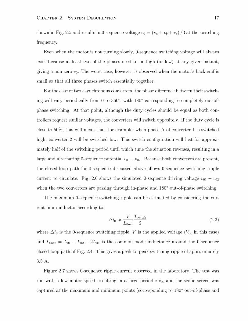
shown in Fig. 2.5 and results in 0-sequence voltage v0 = (va + vb + vc) /3 at the switching
frequency.
Even when the motor is not turning slowly, 0-sequence switching voltage will always
exist because at least two of the phases need to be high (or low) at any given instant,
giving a non-zero v0. The worst case, however, is observed when the motor’s back-emf is
small so that all three phases switch essentially together.
For the case of two asynchronous converters, the phase difference between their switch-
ing will vary periodically from 0 to 360, with 180 corresponding to completely out-of-
phase switching. At that point, although the duty cycles should be equal as both con-
trollers request similar voltages, the converters will switch oppositely. If the duty cycle is
close to 50%, this will mean that, for example, when phase A of converter 1 is switched
high, converter 2 will be switched low. This switch configuration will last for approxi-
mately half of the switching period until which time the situation reverses, resulting in a
large and alternating 0-sequence potential v01−v02. Because both converters are present,
the closed-loop path for 0-sequence discussed above allows 0-sequence switching ripple
current to circulate. Fig. 2.6 shows the simulated 0-sequence driving voltage v01 − v02
when the two converters are passing through in-phase and 180 out-of-phase switching.
The maximum 0-sequence switching ripple can be estimated by considering the cur-
rent in an inductor according to:
∆i0 ≈V
L0net
Tswitch
2(2.3)
where ∆i0 is the 0-sequence switching ripple, V is the applied voltage (Vdc in this case)
and L0net = L01 + L02 + 2Ldc is the common-mode inductance around the 0-sequence
closed-loop path of Fig. 2.4. This gives a peak-to-peak switching ripple of approximately
3.5 A.
Figure 2.7 shows 0-sequence ripple current observed in the laboratory. The test was
run with a low motor speed, resulting in a large periodic v0, and the scope screen was
captured at the maximum and minimum points (corresponding to 180 out-of-phase and

Chapter 2. System Description 18
in-phase switching). This result agrees very well with the approximation of Eqn. (2.3).
A similar test performed in simulation showed a very similar response.
2.6 Chapter Conclusion
Simulations based on the system described here correspond well with laboratory re-
sults, indicating that the salient features have been captured. This is true both for
low-frequency and switching ripple currents.
The periodic variation in the 0-sequence switching current could be eliminated by
adding the common-mode capacitor CCM at the PCC. If sized appropriately, this would
cause a constant 0-sequence switching ripple current even in the single converter case. The
addition of the second converter would have minimal effect on the 0-sequence switching
ripple, as was the case for qd switching currents.
The inductors and capacitors limit the switching frequency ripple current by provid-
ing an impedance in the current path. This switching-frequency ripple current cannot
be controlled by because the converters do not have sufficient bandwidth. The remain-
ing chapters present the control of the low-frequency currents through time-averaged
modelling and control.
Chapter 2. System Description 19
0.1 0.12 0.14 0.16 0.18 0.2 0.22 0.24 0.26 0.28 0.3
−20
0
20
time [s]Voltage
[V] vta1
vtb1vtc1
Magnified Region
(a)
0.187 0.1871 0.1872 0.1873 0.1874 0.1875 0.1876 0.1877 0.1878 0.1879 0.188−1
0
1
time [s]
norm
alize
d
vta1normvtb1normvtc1norm
carrier
(b)
0.187 0.1871 0.1872 0.1873 0.1874 0.1875 0.1876 0.1877 0.1878 0.1879 0.188time [s]
φA switching
φB switching
φC switching
(c)
0.187 0.1871 0.1872 0.1873 0.1874 0.1875 0.1876 0.1877 0.1878 0.1879 0.188−50
0
50
100
150
0.187 0.1871 0.1872 0.1873 0.1874 0.1875 0.1876 0.1877 0.1878 0.1879 0.188−50
0
50
100
150
Voltage
[V]
0.187 0.1871 0.1872 0.1873 0.1874 0.1875 0.1876 0.1877 0.1878 0.1879 0.188−100
0
100
time [s]
vq1
vd1
v01
(d)
Figure 2.5: Explanation of duty cycles for a requested voltage of 0.10 p.u.: (a) Con-
verter 1’s voltage references, highlighting the time period examined in (b)-(d). (b) Re-
quested voltages (normalized against the dc supply voltage vtabc1
vDC/2) and the triangular
carrier signal (c) Duty cycles resulting from the comparison and (d) Instantaneous vqd0
for converter 1.

Chapter 2. System Description 20
0.1792 0.1793 0.1794 0.1795 0.1796 0.1797 0.1798 0.1799 0.18 0.1801 0.1802−100
−50
0
50
100
time [s]
Voltage
[V]
v01 - v02
(a)
0.187 0.1871 0.1872 0.1873 0.1874 0.1875 0.1876 0.1877 0.1878 0.1879 0.188−100
−50
0
50
100
time [s]
Voltage
[V]
v01 - v02
(b)
Figure 2.6: The (a) minimum and (b) maximum 0-sequence driving voltage when two
asynchronous converters are present, corresponding to the region around in-phase and
180 out-of-phase switching, respectively. As in Fig. 2.5, the requested voltage was
0.10 p.u.

Chapter 2. System Description 21
(a)
(b)
Figure 2.7: Experimentally observed 0-sequence ripple current, 6.7 A/V (i.e. 0.67 A/div).
(a) Minimum ripple, corresponding to the converters near in-phase and (b) maximum
ripple, when the converters are switching 180 out-of-phase.
Chapter 3
System Model
3.1 Overview
In this chapter a linearized state-space model of a two converter system driving a single
PMSM is developed. The chapter focuses on the development of an open loop model
that can be interfaced to any specified controller equations. A proposed control design
approach will follow in Chapter 4, along with the development of an associated closed-
loop linearized model.
Section 3.2 identifies the PMSM equations, starting with the rotating reference frame
which was chosen and the rationale for that choice. Section 3.3 develops the averaged
converter models in the qd and 0 reference frames. This leads into Section 3.4, where
the state-space qd model of the converters plus machine is derived. Section 3.5 derives
the 0-sequence state-space model. The chapter concludes with the complete state-space
description of the system in Section 3.6.
3.2 Machine Model
In this section the machine equations transformed into the rotating reference frame
aligned with the machine’s rotor are presented. First, the specific equations used to
22
Chapter 3. System Model 23
transform abc-frame quantities into the rotating qd0-frame quantities are given as multi-
ple transforms exist in the literature. The state equations and the relationships between
voltages and currents used for simulation and control are then presented.
3.2.1 Rotating qd0 Reference Frame
Choosing a rotating reference frame aligned with the machine’s rotor gives non time-
varying inductances and allows for a linear control approach. This choice of reference
frame is an integral part of conventional brushless dc, or field-oriented, control. The
transformation and resulting machine equations are taken from [19].
The transform from the stationary (stator-side) abc-frame into the rotating qd0-frame
is from Eqn. (6.9-17) in [19]:
fqd0 = Kfabc (3.1)
fabc = K−1fqd0 (3.2)
where
K =2
3
cos θ cos(θ − 2π/3) cos(θ + 2π/3)
sin θ sin(θ − 2π/3) sin(θ + 2π/3)
1/2 1/2 1/2
(3.3)
and
K−1 =
cos θ sin θ 1
cos(θ − 2π/3) sin(θ − 2π/3) 1
cos(θ + 2π/3) sin(θ + 2π/3) 1
(3.4)
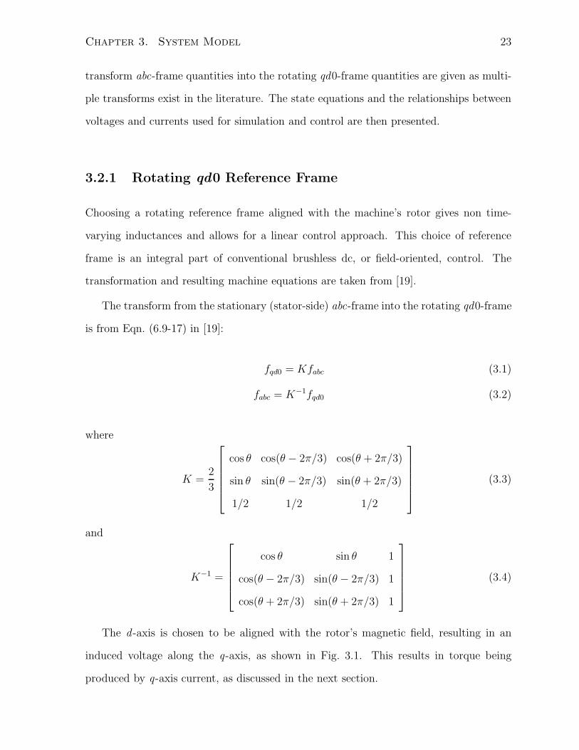
The d -axis is chosen to be aligned with the rotor’s magnetic field, resulting in an
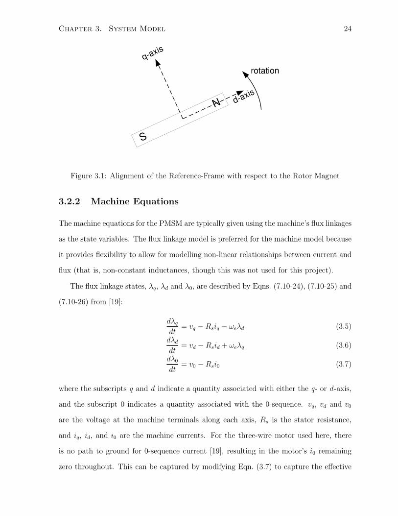
induced voltage along the q-axis, as shown in Fig. 3.1. This results in torque being
produced by q-axis current, as discussed in the next section.
Chapter 3. System Model 24
S
N
rotation
d-axis
q-axis
Figure 3.1: Alignment of the Reference-Frame with respect to the Rotor Magnet
3.2.2 Machine Equations
The machine equations for the PMSM are typically given using the machine’s flux linkages
as the state variables. The flux linkage model is preferred for the machine model because
it provides flexibility to allow for modelling non-linear relationships between current and
flux (that is, non-constant inductances, though this was not used for this project).
The flux linkage states, λq, λd and λ0, are described by Eqns. (7.10-24), (7.10-25) and
(7.10-26) from [19]:
dλq
dt= vq − Rsiq − ωeλd (3.5)
dλd
dt= vd − Rsid + ωeλq (3.6)
dλ0
dt= v0 − Rsi0 (3.7)
where the subscripts q and d indicate a quantity associated with either the q- or d -axis,
and the subscript 0 indicates a quantity associated with the 0-sequence. vq, vd and v0
are the voltage at the machine terminals along each axis, Rs is the stator resistance,
and iq, id, and i0 are the machine currents. For the three-wire motor used here, there
is no path to ground for 0-sequence current [19], resulting in the motor’s i0 remaining
zero throughout. This can be captured by modifying Eqn. (3.7) to capture the effective

Chapter 3. System Model 25
resistance to ground through the motor:
dλ0
dt= v0 − (Rs + R0) i0 (3.8)
where R0 → ∞ because of the three-wire motor.
When the magnetics are linear, the flux linkages can be expressed in terms of the
inductances and currents according to λq = Lqiq, λd = Ldid + λ′
m and λ0 = L0i0, giving:
Lqdiqdt
= vq − Rsiq − ωe (Ldid + λ′
m)
Lddiddt
= vd − Rsid + ωeLqiq (3.9)
L0di0dt
= v0 − (Rs + R0) i0
with λ′
m the amplitude of the flux linkages generated by the permanent magnets referred
to the stator side.
Isolating the voltages on the left-hand side of Eqn. (3.9) gives:
vq = Lqdiqdt
+ Rsiq + ωe (Ldid + λ′
m)
vd = Lddiddt
+ Rsid − ωeLqiq (3.10)
v0 = L0di0dt
+ (Rs + R0) i0
To completely describe the machine, the equations relating the electrical and me-
chanical states and the equations describing the mechanical states are also required. The
developed torque Te is given by Eqn. (7.10-35) from [19]:
Te =3
2
p
2λ′
miq (3.11)
where p is the number of poles. Notice that the machine torque is proportional to, and
is only a function of, iq1. The machine speed and torque are related by:
d
dtωr =
Te − TL
J(3.12)
1This allows the coordinate transform to be properly oriented (as in Fig. 3.1). To orient the rotor’sd -axis with respect to the encoder’s reset, the fact that no torque results from non-zero id is exploited: alarge current space vector is applied to the machine and when no torque is produced, the space vector isaligned with the d -axis (or the negative d -axis). The significance of the negative d -axis is that a positiveiq will result in negative speed.

Chapter 3. System Model 26
where TL is the load torque and J is the rotor plus load inertia. The electrical speed ωe,
in [electrical rad./s], is related to the mechanical rotor speed ωr according to:
ωe = ωrp
2(3.13)
The electrical speed is chosen as a state variable instead of the mechanical speed because
all the electrical calculations depend on ωe. The speed state equation, from Eqns. (3.11),
(3.12) and (3.13), is given by:
d
dtωe =
p
2
(
3p4λ′
miq − TL
J
)
(3.14)
3.2.3 Input-Output Block for Machine Equations
These machine equations describe an input-output block of the form shown in Fig. 3.2
where vqd0 and iqd0 are related by Eqn. (3.10) and ωe is related to iqd0 by Eqn. (3.14). In
these two sets of equations the 0-sequence quantities are decoupled from the qd quanti-
ties. This allows the overall input-output block to be replaced with two separate blocks,
Fig. 3.3, that are used to represent the machine in the development of the overall state-
space system model.
ω
Figure 3.2: The qd0 motor block.

Chapter 3. System Model 27
ω
(a)
(b)
Figure 3.3: The separate (a) qd and (b) 0-sequence motor input/output blocks.
3.3 Averaged Converter Circuit
To simplify the development of the state-space model of the two-converter system the
averaged qd and 0-sequence converter models are developed in this section. These mod-
els allow the formulation of simplified differential equations relating the converter and
machine quantities. The separation of the qd and 0-sequence models is justified because
applying the qd0 reference frame transformation of Section 3.2.1 to a single converter
results in a decoupled system. Additionally, the motor qd and 0-sequence components
were demonstrated to be decoupled in the previous section.
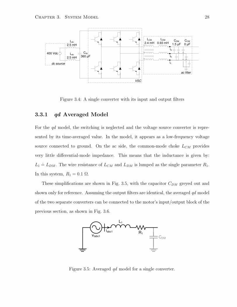
Fig. 3.4 shows a single converter plus its input and output filters (from the two-
converter system, Fig. 2.1). The averaged converter model is a simplification of this
circuit and has to be valid for those frequencies at which the motor operates, given by
ωe. In this case, the upper limit is 100 Hz and the lower limit is approximately dc.
At these frequencies, the output capacitor CDM (and CCM , were it present), which is
sized to suppress EMI, has high impedance and can be neglected. The dc source can be
treated as ideal because the capacitor Csource is large enough that even at low frequencies
its impedance is low. For very low frequencies, the impedance of the diode rectifier and
the chokes Lsource is very low, meaning this approximation remains valid.
Further simplifications necessitate examining the qd - and 0-sequence separately, as
was done for the switching ripple in Chapter 2. This is done in the next two sections.
Chapter 3. System Model 28
Cdc
360 μF
LDM
0.93 mHCDM
1.5 μF
LCM
2.4 mH
VSC
ia
ib
ic
CCM
0 μF
ac filter
400 Vdc
dc source
Ldc
2.5 mH
Ldc
2.5 mH
Figure 3.4: A single converter with its input and output filters
3.3.1 qd Averaged Model
For the qd model, the switching is neglected and the voltage source converter is repre-
sented by its time-averaged value. In the model, it appears as a low-frequency voltage
source connected to ground. On the ac side, the common-mode choke LCM provides
very little differential-mode impedance. This means that the inductance is given by:
L1.= LDM . The wire resistance of LCM and LDM is lumped as the single parameter R1.
In this system, R1 = 0.1 Ω.
These simplifications are shown in Fig. 3.5, with the capacitor CDM greyed out and
shown only for reference. Assuming the output filters are identical, the averaged qd model
of the two separate converters can be connected to the motor’s input/output block of the
previous section, as shown in Fig. 3.6.
vtabc1
L1
R1iabc1
CDM
Figure 3.5: Averaged qd model for a single converter.

Chapter 3. System Model 29
vtqd1
L1
R1iqd1
iqd
+ vqd -
vtqd2
L1
R1iqd2
PMSM
e
Figure 3.6: Averaged qd model for the two-converter system
3.3.2 0-Sequence Averaged Model
In Section 2.5.3 the 0-sequence current path, which depends on the presence of both
converters, was introduced. To reiterate the findings there: on the ac side, the differential-
mode inductor LDM does not affect the 0-sequence current, resulting in an inductance
of L01.= LCM . On the dc side, the impedance is 2Ldc. The lumped resistance R1
corresponding to the ac inductors is the same as in the qd model.
Connecting the 0-sequence motor input/output block gives the averaged 0-sequence
converter model of Fig. 3.7.
vt01
vt02
L01
L01
R1
R1
i01
i02
Ldc
Ldc
i0
+ v0 -
PMSM
Figure 3.7: Averaged model of the 0-sequence circuit.

Chapter 3. System Model 30
3.4 qd Model of the Parallel Converter Arrangement
This section derives the linearized state-space model for the qd currents in the open-loop
system. The basis for this derivation is the averaged converter model coupled with the
motor, shown in Fig. 3.6.
Section 3.5 gives the 0-sequence state-space model to complete the description of the
open-loop two-converter motor drive.
3.4.1 qd State-Space Derivation
The conventions shown in Fig. 3.6 cause the motor currents iqd, which are normally
chosen as states, to be linear combinations of the converter currents:
iq = iq1 + iq2 (3.15)
id = id1 + id2
The state vector xqd of the combined motor-converter qd system is chosen as:
xqd =
[
ωe iq1 id1 iq2 id2
]T
(3.16)
This choice was made in order to allow the local controllers to control local state variables
and simplifies the extension of the analysis to the case where more than two converters
are present.
Solving the circuit relations gives expressions for the qd currents in converters 1 and 2.
The differential equations are expressed as a function of the state variables, the control
voltages vtqd1 and vtqd2, and the motor terminal voltage vqd:
L1d
dtiq1 = −R1iq1 − ωeL1id1 − vq + vtq1
L1d
dtid1 = ωeL1iq1 − R1id1 − vd + vtd1 (3.17)
L1d
dtiq2 = −R1iq2 − ωeL1id2 − vq + vtq2
L1d
dtid2 = ωeL1iq2 − R1id2 − vd + vtd2

Chapter 3. System Model 31
These equations are non-linear because ωe, iq1,2 and id1,2 are all state variables. Note
that in this form converter 1 is not coupled to converter 2 directly. The coupling occurs
through the motor, appearing through the voltage vqd.
The machine description, Eqn. (3.10), is used to rewrite vqd in terms of the state
variables. This yields:
vq = Lqd
dt(iq1 + iq2) + Rs (iq1 + iq2) + ωe
(
Ld (id1 + id2) + λ′
m
)
(3.18)
vd = Ldd
dt(id1 + id2) + Rs (id1 + id2) − ωeLq (iq1 + iq2)
The open-loop state equations are obtained by substituting Eqn. (3.18) into Eqn. (3.17)
and augmenting that system with Eqn. (3.14), the state equation for ωe, with iq = iq1+iq2:
Ld
dt
ωe
iq1
id1
iq2
id2
=
3p2
8λ′
m (iq1 + iq2)
− (R1 + Rs) iq1 − Rsiq2 − ωe
(
(L1 + Ld) id1 + Ldid2 + λ′
m
)
− (R1 + Rs) id1 − Rsid2 + ωe
(
(L1 + Lq) iq1 + Lqiq2)
−Rsiq1 − (R1 + Rs) iq2 − ωe
(
Ldid1 + (L1 + Ld) id2 + λ′
m
)
−Rsid1 − (R1 + Rs) id2 + ωe
(
Lqiq1 + (L1 + Lq) iq2)
+
−pTL
2J
vtq1
vtd1
vtq2
vtd2
(3.19)
Linearizing about an operating point (with large signal values denoted by a bar, e.g.
ωe) gives the system in a linear state-space form:
Ld
dt
ωe
iq1
id1
iq2
id2
=
0 3p2
8λ′
m 0 3p2
8Jλ′
m 0
A32 −Rt −ωeLdt −Rs −ωeLd
A42 −ωeLqt −Rt ωeLq −Rs
A52 −Rs −ωeLd −Rt −ωeLdt
A62 −ωeLq −Rs ωeLqt −Rt
ωe
iq1
id1
iq2
id2
+
−pTL
2J
vtq1
vtd1
vtq2
vtd2
(3.20)

Chapter 3. System Model 32
with Rt = R1 + Rs, Ldt = L1 + Ld, Lqt = L1 + Lq and:
L =
1 0 0 0 0
0 Lqt 0 Lq 0
0 0 Ldt 0 Ld
0 Lq 0 Lqt 0
0 0 Ld 0 Ldt
A32 = −Ldtid1 − Ldid2 − λ′
m A42 = −Lqtiq1 − Lqiq2
A52 = −Ldid1 − Ldtid2 − λ′
m A62 = −Lqiq1 − Lqtiq2
The sparse leading matrix L results from the differentials in the motor voltage equations
which depend on both converters. Inverting L:
L−1 =
1 0 0 0 0
0 L1+Lq
L1(L1+2Lq)0 −Lq
L1(L1+2Lq)0
0 0 L1+Ld
L1(L1+2Ld)0 −Ld
L1(L1+2Ld)
0 −Lq
L1(L1+2Lq)0 L1+Lq
L1(L1+2Lq)0
0 0 −Ld
L1(L1+2Ld)0 L1+Ld
L1(L1+2Ld)
(3.21)
and pre-multiplying gives the small-signal state-space qd model for the open-loop two-
converter system:
d
dtxqd = Aqdxqd + Bqduqd (3.22)

Chapter 3. System Model 33
where
Aqd =
0 3p2
8Jλ′
m 0 3p2
8Jλ′
m 0
A32 −R1Lqt+RsL1
L1(L1+2Lq)−ωe(L1+Lq+Ld)
L1+2Lq
R1Lq−RsL1
L1(L1+2Lq)ωe(Lq−Ld)
L1+2Lq
A42ωe(L1+Lq+Ld)
L1+2Ld−R1Ldt+RsL1
L1(L1+2Ld)ωe(Lq−Ld)
L1+2Ld
R1Ld−RsL1
L1(L1+2Ld)
A52R1Lq−RsL1
L1(L1+2Lq)ωe(Lq−Ld)
L1+2Lq−R1Lqt+RsL1
L1(L1+2Lq)−ωe(L1+Lq+Ld)
L1+2Lq
A62ωe(Lq−Ld)
L1+2Ld
R1Ld−RsL1
L1(L1+2Ld)
ωe(L1+Lq+Ld)
L1+2Ld−R1Ldt+RsL1
L1(L1+2Ld)
Bqd =
− p2J
0 0 0 0
0 Lqt
L1(L1+2Lq)0 −Lq
L1(L1+2Lq)0
0 0 Ldt
L1(L1+2Ld)0 −Ld
L1(L1+2Ld)
0 −Lq
L1(L1+2Lq)0 Lqt
L1(L1+2Lq)0
0 0 −Ld
L1(L1+2Ld)0 Ldt
L1(L1+2Ld)
uqd =
[
TL vtq1 vtd1 vtq2 vtd2
]T
A32 = −(L1 + Lq + Ld) id1 + (Ld − Lq) id2 + λ′
m
L1 + 2Lq
A42 = −(L1 + Lq + Ld) iq1 + (Lq − Ld) iq2
L1 + 2Ld
A52 = −(Ld − Lq) id1 + (L1 + Lq + Ld) id2 + λ′
m
L1 + 2Lq
A62 = −(Lq − Ld) iq1 + (L1 + Lq + Ld) iq2
L1 + 2Ld
Examining Aqd shows the response of converter 1 to iqd1 is identical to the response of
converter 2 to iqd2 and vice-versa, which is as expected. The interactions with the motor
(A32, A42, A52 and A62) are also in agreement. This confirms that from the system’s

Chapter 3. System Model 34
perspective the two converters are identical. The Aqd matrix shows that converter 1 is
closely coupled to converter 2. The matrix Bqd shows that converter 2’s control voltages
have almost as much impact on converter 1 as do converter 1’s voltages. This makes the
control problem more difficult because when the converters are independent converter 1
does not have access to converter 2’s control voltages without additional sensing circuitry.
3.5 0-Sequence Model of the Parallel Converter
Arrangement
This section develops the state-space model for the 0-sequence currents.
The convention for current in Fig. 3.7 relates the converter and motor currents:
i0 = i01 + i02 (3.23)
From the discussion of the equations describing the motor’s input/output block, Fig. 3.3b,
recall that the impedance to ground through the block is very large (as R0 → ∞). This
results in i0 = 0, which gives, from Eqn. (3.23):
i01 = −i02 (3.24)
This means that the 0-sequence current is a state common to both converters.
The equations describing this state can be derived using KCL applied around the
closed loop path:
vt01 − vt02 = (2L01 + 2Ldc)d
dti01 + 2R1i01 (3.25)
where the resistance associated with Ldc is assumed to be small. Rearranging and adopt-
ing the conventions L0net = 2L01 + 2Ldc and R0net = 2R1 gives:
d
dti01 = −
R0net
L0neti01 + vt01 − vt02 (3.26)
This is the state-space description of the low-frequency 0-sequence current.
Chapter 3. System Model 35
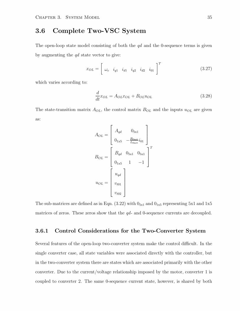
3.6 Complete Two-VSC System
The open-loop state model consisting of both the qd and the 0-sequence terms is given
by augmenting the qd state vector to give:
xOL =
[
ωe iq1 id1 iq2 id2 i01
]T
(3.27)
which varies according to:
d
dtxOL = AOLxOL + BOLuOL (3.28)
The state-transition matrix AOL, the control matrix BOL and the inputs uOL are given
as:
AOL =
Aqd 05x1
01x5 −R0net
L0net
i01
BOL =
Bqd 05x1 05x1
01x5 1 −1
T
uOL =
uqd
vt01
vt02
The sub-matrices are defined as in Eqn. (3.22) with 05x1 and 01x5 representing 5x1 and 1x5
matrices of zeros. These zeros show that the qd - and 0-sequence currents are decoupled.
3.6.1 Control Considerations for the Two-Converter System
Several features of the open-loop two-converter system make the control difficult. In the
single converter case, all state variables were associated directly with the controller, but
in the two-converter system there are states which are associated primarily with the other
converter. Due to the current/voltage relationship imposed by the motor, converter 1 is
coupled to converter 2. The same 0-sequence current state, however, is shared by both

Chapter 3. System Model 36
converters. It is also completely decoupled from the rest of the system. These issues are
addressed in the next chapter.

Chapter 4
Controller Development
4.1 Control Methodology
The control objective is regulation of the motor speed using two independently controlled
converters. Each converter controller receives position feedback from the motor. Each
controller is also supplied with the same reference speed. Without inter-converter com-
munication, each converter has access only to its own converter’s output currents and
local dc-bus voltage (Cdc voltage).
In order to facilitate speed regulation using linear control techniques and to exploit
the decoupling between the qd and 0-sequence quantities, the two-converter system is
controlled using field-oriented control techniques. The system state variables for control
are the qd0 currents for each converter, the machine speed, and whatever states are
associated with the control. In order to have the 0-sequence voltage as a control parameter
for the voltage-sourced converters, sinusoidal PWM (SPWM) is used rather than space-
vector modulation (SVM).
To implement a fully modular system, the controllers are required to be both indepen-
dent and scalable. To address scalability, it is desired that the same control be applied
to each converter. To ascertain whether the closed-loop system is stable, an eigenvalue
37
Chapter 4. Controller Development 38
analysis was performed.
Two challenges were expected as a result of the literature review. First, it is necessary
that the converters share current equally transiently and in steady-state. The current
sharing is not inherent because the converters act as stiff voltage sources, and it is possible
to set up a significant circulating current while maintaining a specified operating point
of the motor.
Second, the converters are able to produce a 0-sequence voltage. Use of two converters
on the same dc- and ac-buses without isolation provides a path for 0-sequence current
to flow. This current has no path through the motor, so it has no direct impact on
the motor’s operation, but this circulating 0-sequence current introduces extra losses
into the system and reduces the maximum q- and d -axis currents which the converter
can supply. Contrary to the 0-sequence switching ripple discussed in Chapter 2 which
is predominantly influenced by reactor design, circulation of low frequency 0-sequence
current must be mitigated through control action.
The 0-sequence control is developed in Section 4.2. The problem of the machine
control, which consists of a speed regulator and current controllers for the q- and d -axes,
is presented in Section 4.3. Section 4.4 develops the closed-loop state-space model of the
linearized system. The stability of the resulting system is analyzed in Section 4.5.
4.2 0-Sequence Control
As the 0-sequence quantities are decoupled from the qd quantities in Eqn. (3.28), the
0-sequence quantities can be controlled independently from the machine quantities. This
also indicates that the 0-sequence current has no direct impact on the control objective.
Instead, the 0-sequence current can be thought of as a parasitic, where the control tries
to minimize the value of this parasitic.
The time-averaged 0-sequence current results from slight differences in converter dead-
Chapter 4. Controller Development 39
times and other non-idealities. Any 0-sequence current which flows eats into the maxi-
mum current which can flow in any given switch and increases losses without contributing
to any control objective, and thus ideally the time-averaged 0-sequence current should
be zero.
4.2.1 Proposed 0-Sequence Controller
The 0-sequence model, Eqn. (3.26), has two control inputs while there is only a single
state to be controlled. The feedback control loop is shown in Fig. 4.1. Choosing both
controllers C01(s) = C02(s).= C0(s) maintains the modular approach. The signals err1
and err2 represent sensor errors and noise in the circuit. If either is non-zero, then
choosing a PI control for C0(s) will result in integral wind-up even if the references are
equal.
Figure 4.1: 0-sequence feedback control model
For this reason, a proportional control C0(s) = k0 is chosen such that:
vt01 = −k0i01 (4.1)
vt02 = −k0i02
The references i∗01 and i∗02 are set to zero. The closed-loop 0-sequence model is then given
Chapter 4. Controller Development 40
by:
d
dti01 = −
R0net + 2k0
L0neti01 (4.2)
which is stable for all k0 ≥ −R0net/2. Assuming that both controllers are identical, as
has been done here, allows k0 to be tuned as if there is only one controller with a plant
of 2/ (sL0net + R0net).
Unlike the development in Section 2.5.4 where the 0-sequence switching ripple was
examined, the control in this section is for low-frequency 0-sequence current. Although
the impedance seen by the switching ripple and the averaged model is the same, the
converters do not have sufficient bandwidth to control the switching ripple and the con-
troller developed here must not respond to switching-frequency 0-sequence current. If
the bandwidth is too high, then the low-frequency assumptions can be violated, resulting
in the performance of the qd control being degraded. This places a limit on the maxi-
mum viable value of k0. In this project, the chosen k0 yields a closed-loop bandwidth of
approximately fswitch/100.
4.3 Machine Control
Although the 0-sequence control is important, the control objective is regulation of the
motor speed. To accomplish this, the quadrature currents must be regulated appropri-
ately.
4.3.1 Conventional Single Converter Field-Oriented Control
For the single converter case, conventional field-oriented control can be used to regulate
the speed when position feedback is available [20]. Field-oriented control is outlined
briefly in this section. The converter currents are equal to the machine currents, so
controlling the converter currents directly controls the machine currents.
The machine torque Te is proportional to iq. Speed regulation is achieved using an
Chapter 4. Controller Development 41
outer control loop to assign i∗q. By using PI-controllers, the speed and q-axis current
can be forced to track their references with zero steady-state error (in the presence of
step-changes). Although iq is forced to track its reference, this capability is not strictly
necessary because the speed controller will automatically adjust its output (i∗q) if there
is a difference between the speed and its reference.
To achieve maximum torque per unit current, id is controlled to zero. This results in
the closed-loop control structure for the single-converter case shown in Fig. 4.2. In order
to decouple the q- and d -axis currents from each other, the cross-coupling terms are fed
forward.
Figure 4.2: Conventional single-converter field-oriented control loop
Assuming proper tuning of all PI gains, the resulting system exhibits a fast response
and is stable.
4.3.2 Extension to the Two-Converter Case
The conventional field-oriented control is adapted for the two-converter case. The ad-
dition of the second converter adds the need to maintain system stability and ensure
both dynamic and steady-state load-sharing. Adding a second converter also creates a
path for 0-sequence current. Fortunately, the 0-sequence quantities are decoupled and
Chapter 4. Controller Development 42
are controlled using the method developed in Section 4.2.1.
By examining the open-loop system of Eqn. (3.28), it is can be seen that each converter
k’s currents iqk and idk are closely coupled, through the motor, to the q- and d -axis
currents in the other converter(s). As well, each converter’s currents are directly impacted
by the other converter’s control voltage through the BOL-matrix. This is potentially
problematic because each converter has knowledge only of its own currents iqk and idk,
effectively preventing a proper cancellation of the cross-coupling between the q- and
d -axis currents.
In order to address the need for steady-state current sharing, a droop term is added
to the speed PI-control loop to account for any speed measurement errors. As in the
single converter case, there is no need to put a droop on the q-axis current PI-controller.
i∗qk will be modified by each converter’s speed control loop as required. If the system is
stable, dynamic load-sharing occurs as a result of the identical controllers. This choice
of control maintains modularity and does not require inter-converter communication.
System stability is verified in Section 4.5.
Unlike the 0-sequence case, no droop is required for the d -axis current PI-control loop
because the motor is able to sink any current which results from sensor errors or noise.
The proposed control loop is shown in Fig. 4.3.
The values to use for the cancellation of the cross-coupling L terms can be chosen
based on the closed-loop two-converter model presented in the next section. Converter 1
and converter 2 use identical controllers, so Cq1(s) = Cq2(s).= Cq(s) and Cd1(s) =
Cd2(s).= Cd(s). The speed-control loop controllers are equal also: Cω1(s) = Cω2(s)
.=
Cω(s).

Chapter 4. Controller Development 43
ω
ω
ω
ω
ω
ω
ω
ω
ω
ω
ω
Figure 4.3: Field-oriented control loop extended for the parallel converter system
4.4 Closed-Loop Two-Converter System Model
The model developed in this section closes the loop for the system of Eq. (3.28) using
the control described in the previous section, with particular reference to Fig. 4.3. For
each converter k, that control can be summarized as:
• PI-control feedback Cd(s) is applied to idk to set vtdk with the references i∗dk = 0
for each converter with feed-forward terms to cancel some of the coupling with the
q-axis
• PI-control feedback is applied to iqk to set vtqk with the references i∗qk set by the
speed control loops with feed-forward terms to cancel some of the coupling with
the d -axis
• Drooped PI-control applied to ωe to set i∗qk with the reference ω∗
e set externally

Chapter 4. Controller Development 44
The presence of three PI-control loops (per controller) adds three states per controller to
the system. These will be donated as xsk, for the speed controllers’ integrators, and xqk
and xdk for the q- and d -axis controllers’ integrators.
In order to close the loop, the values of control inputs need to be specified. From uOL
in Eq. (3.28), these inputs are: vtqk, vtdk, vt0k (for each converter) and TL. The voltages
are the control inputs while TL is the mechanical loading supplied by the dynamometer
and is described by Eq. (2.2) for a resistively loaded dc machine. For the purposes of the
closed-loop analysis, kL = 0.05 is assumed.
4.4.1 Speed Control Loop
The drooped PI-control used for the speed loop, giving the i∗qk, has this transfer function
where the PI is given by Cω(s) = kω(s + aω)/s:
i∗qk =kω (s + aω)
s (1 + kωDω) + kωaωDω(ω∗
e − ωe) (4.3)
where Dω is the droop coefficient. This can be rewritten in state-space form, with the
state xsk = ω∗
e − ωe − Dωi∗qk described by:
d
dtxsk =
1
1 + kωDω
(ω∗
e − ωe) −kωaωDω
1 + kωDω
xsk (4.4)
The output from the speed control loop is given by:
i∗qk =kω
1 + kωDω
(ω∗
e − ωe) +kωaω
1 + kωDω
xsk (4.5)
4.4.2 q-axis Control Loop
The closed-loop q-axis control loop depends on i∗qk, and defines the control voltage vtqk
using this transfer function:
vtqk =(
i∗qk − iqk
) kq (s + aq)
s+ ωeLcdidk (4.6)
Chapter 4. Controller Development 45
where Lcd is the inductance associated with the cancelled cross-coupling term, and is free
to be chosen. The state-space model in terms of the integrator state xqk using Eq. (4.5)
for i∗qk is:
d
dtxqk = i∗qk − iqk
=kω
1 + kωDω
(ω∗
e − ωe) +kωaω
1 + kωDω
xsk − iqk (4.7)
The output voltage is written in state-space form by subbing Eq. (4.5) into Eq. (4.6):
vtqk = kqaqxqk + kq
(
kω
1 + kωDω(ω∗
e − ωe) +kωaω
1 + kωDωxsk
)
− kqiqk + ωeLcdidk
= kqaqxqk +kqkωaω
1 + kωDω
xsk +kqkω
1 + kωDω
(ω∗
e − ωe) − kqiqk + ωeLcdidk (4.8)
Linearizing gives the converter voltage:
vtqk = kqaqxqk +kqkωaω
1 + kωDωxsk +
kqkω
1 + kωDω(ω∗
e − ωe)− kqiqk + ωeLcdidk + idkLcdωe (4.9)
completing the description of the q-axis closed-loop control voltage.
4.4.3 d-axis Control Loop
The closed-loop d -axis control loop always has zero input and defines the output control
voltage vtdk according to the transfer function:
vtdk = −idkkd (s + ad)
s+ ωeLcqiqk (4.10)
Using the state xdk, defined as:
d
dtxdk = −idk (4.11)
allows the state-space description for the d -axis control voltage:
vtdk = kdadxdk − kdidk − ωeLcqiqk (4.12)
Linearizing gives:
vtdk = kdadxdk − kdidk − ωeLcqiqk − iqkLcqωe (4.13)
Chapter 4. Controller Development 46
4.4.4 Closed-Loop Model
The overall closed-loop model is shown in Fig. 4.4.
The control voltages given in Eqns. (4.1), (4.9), (4.13) and the loading description
Eqn. (2.2), define the control inputs in uOL. Along with the control matrix BOL, these
allow the closed-loop feedback control to be described.
The augmented closed-loop model uses the state vector x:
x =
[
ωe iq1 id1 iq2 id2 i01 xs1 xq1 xd1 xs2 xq2 xd2
]T
(4.14)
Later, it will be advantageous to re-order the state vector and associated closed-loop state-
transition matrix to group the qd states for a single converter-controller pair together,
followed by the differential-mode 0-sequence state i01.
The only remaining input to this system is ω∗
e . The control parameters, introduced
in the previous sections, are kω, aω and Dω (speed loop), Lcd, kq and aq (q-axis current
loop), and Lcq, kd and ad (d -axis current loop). The closed-loop form is given by:
d
dtx = Ax + Bu (4.15)
with u = ω∗
e .
Reordering the state vector x to xCL where:
xCL =
[
ωe iq1 id1 xs1 xq1 xd1 iq2 id2 xs2 xq2 xd2 i01
]T
(4.16)
gives:
d
dtxCL = ACLxCL + BCLu (4.17)
with u = u. This allows the system to be more easily extended to the case of more than
two converters because the states associated with each converter’s qd model are grouped
together. First, this means that another converter can be added without a complicated
reordering of the state-transition matrix. Second, that inter-converter interactions can
be identified.

Chapter 4. Controller Development 47
C_w(s)
C_q(s)
qd0>abc
+
C_d(s)+
idref=0
Composite
Plant:SPW
Mgating
inputreactorsSM
with
load
vta1
vtb1
vtc1C_0(s)
+
i0ref=0
Mult.
L_d
+
w
ib1
ic1
ia1
abc>qd0
Mult.
id1
i01
iq1 L_q
wid1
iq1w
+
LPF
wref +
vta2
vtb2
vtc2
D_w
iqref
vsa2vsb2
vsc2
wiq1
id1i01
ia2
ib2
ic2
Figure 4.4: Overall controller flow diagram

Chapter 4. Controller Development 48
The significance of the placement of ωe at the beginning of and i01 at the end of the
state vector will be discussed in Section 4.5.2.
This choice of xCL causes the ACL matrix to have the form:
ACL =
−pkL
2J A1ω A2ω
Aω1
A11 A21
Ac1 03x5
Aω2
A12 A22
03x5 Ac2
011x1
01x11 A0
(4.18)
The first row shows how the speed is affected by itself (through the dynamometer
loading −pkL
2J) and the converter currents/integrator states through A1ω and A2ω. Because
both converters contribute identically to the machine currents, A1ω = A2ω.= Acω.
The speed affects the converter currents and integrator states through Aω1 and Aω2.
Converter 1’s currents interact with themselves and with the converter 1’s integrators
through A11, and with converter 2’s states through A21. The zeros (03x5) indicate that
converter 1’s integrators interact only with the states associated with converter 1, which
is as expected based on the independent control approach.
The state-transition matrices associated with converter 2 are mirrors of those as-
sociated with converter 1, meaning that A22 = A11.= As, A21 = A12
.= An and
Ac1 = Ac2.= Ac. Aω1 and Aω2 are not equal as they depend on large signal quanti-
ties (e.g. iq1), but they mirror each other. The final column and final row of zeros
correspond to the 0-sequence current which is decoupled from the rest of the system.
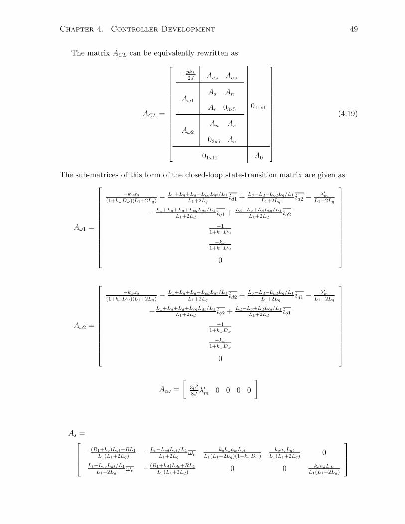
Chapter 4. Controller Development 49
The matrix ACL can be equivalently rewritten as:
ACL =
−pkL
2J Acω Acω
Aω1
As An
Ac 03x5
Aω2
An As
03x5 Ac
011x1
01x11 A0
(4.19)
The sub-matrices of this form of the closed-loop state-transition matrix are given as:
Aω1 =
−kωkq
(1+kωDω)(L1+2Lq)− L1+Lq+Ld−LcdLqt/L1
L1+2Lqid1 + Lq−Ld−LcdLq/L1
L1+2Lqid2 −
λ′
m
L1+2Lq
−L1+Lq+Ld+LcqLdt/L1
L1+2Ldiq1 + Ld−Lq+LdLcq/L1
L1+2Ldiq2
−11+kωDω
−kω
1+kωDω
0
Aω2 =
−kωkq
(1+kωDω)(L1+2Lq)− L1+Lq+Ld−LcdLqt/L1
L1+2Lqid2 + Lq−Ld−LcdLq/L1
L1+2Lqid1 −
λ′
m
L1+2Lq
−L1+Lq+Ld+LcqLdt/L1
L1+2Ldiq2 + Ld−Lq+LdLcq/L1
L1+2Ldiq1
−11+kωDω
−kω
1+kωDω
0
Acω =
[
3p2
8Jλ′
m 0 0 0 0
]
As =
− (R1+kq)Lqt+RL1
L1(L1+2Lq)−Lt−LcdLqt/L1
L1+2Lqωe
kqkωaωLqt
L1(L1+2Lq)(1+kωDω)kqaqLqt
L1(L1+2Lq)0
Lt−LcqLdt/L1
L1+2Ldωe − (R1+kd)Ldt+RL1
L1(L1+2Ld)0 0 kdadLdt
L1(L1+2Ld)

Chapter 4. Controller Development 50
with Lt = L1 + Lq + Ld.
An =
(R1+kq)Lq−RL1
L1(L1+2Lq)Lq−Ld−LcdLq/L1
L1+2Lqωe
−kqkωaωLq
L1(L1+2Lq)(1+kωDω)−kqaqLq
L1(L1+2Lq)0
Lq−Ld+LcqLd/L1
L1+2Ldωe
(R1+kd)Ld−RL1
L1(L1+2Ld)0 0 −kdadLd
L1(L1+2Ld)
Ac =
0 0 −kωaωDω
1+kωDω0 0
−1 0 kωaω
1+kωDω0 0
0 −1 0 0 0
A0 = −R0net − 2k0
L0net
The control input matrix BCL is given as:
BCL =
0
kqkω
(L1+2Lq)(1+kωDω)
0
kqkω
(L1+2Lq)(1+kωDω)
0
0
11+kωDω
kω
1+kωDω
0
11+kωDω
kω
1+kωDω
0
(4.20)

Chapter 4. Controller Development 51
4.5 Stability Analysis
4.5.1 Common- and Differential-Mode Currents
The modes relating the converter current to the motor are the common modes of the
system. The common-mode currents iq and id are the sum of the converter currents:
iq =∑
k
iqk (4.21)
id =∑
k
idk
where k is the converter index. Here, k is only 1 and 2 because there are two converters.
The states can be redefined in terms of these common-mode currents. When taken in
concert with the machine speed ωe, which is also a common-mode state, the associated
eigenvalues will dictate the response of the common-mode. As the control objective is
machine control and the common-mode q and d currents are the machine currents, the
common-mode response is of the most interest.
The inter-converter differential-modes are not directly related to a control objective,
but they must be stable. Depending on how the differential-modes are excited, these
modes may not require as much damping as the common modes. The difference currents,
which the differential-modes are associated with, are given by:
iqk,DM = iq/N − iqk (4.22)
idk,DM = id/N − idk
Although differential-mode currents are defined for each converter in the system (in
this case 2 converters) one of these currents is redundant. This was encountered already
for the case of the 0-sequence currents i01 and i02 where i02 was redundant. For the two-
converter case, only the differential-mode currents defined with respect to converter 1 are
chosen as states.
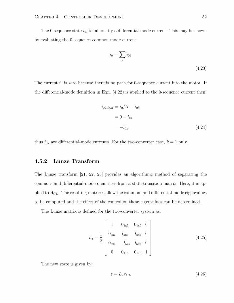
Chapter 4. Controller Development 52
The 0-sequence state i01 is inherently a differential-mode current. This may be shown
by evaluating the 0-sequence common-mode current:
i0 =∑
k
i0k
(4.23)
The current i0 is zero because there is no path for 0-sequence current into the motor. If
the differential-mode definition in Eqn. (4.22) is applied to the 0-sequence current then:
i0k,DM = i0/N − i0k
= 0 − i0k
= −i0k (4.24)
thus i0k are differential-mode currents. For the two-converter case, k = 1 only.
4.5.2 Lunze Transform
The Lunze transform [21, 22, 23] provides an algorithmic method of separating the
common- and differential-mode quantities from a state-transition matrix. Here, it is ap-
plied to ACL. The resulting matrices allow the common- and differential-mode eigenvalues
to be computed and the effect of the control on these eigenvalues can be determined.
The Lunze matrix is defined for the two-converter system as:
Lz =1
2
1 01x5 01x5 0
05x1 I5x5 I5x5 0
05x1 −I5x5 I5x5 0
0 01x5 01x5 1
(4.25)
The new state is given by:
z = LzxCL (4.26)

Chapter 4. Controller Development 53
this gives z =[
zc zd
]
where zc consists of a speed state, the common-mode currents
from Eqn. (4.21) and the common-mode integrator states. zd consists of the differential
qd currents and integrator states plus the 0-sequence current state.
Previously the state vector was reordered so that the machine speed ωe was the first
state and the 0-sequence current i01 was the last. When the Lunze transform is applied,
these single states are not transformed because a sum or difference is not meaningful for a
single state. That the states are identical is evidenced in Eqn. (4.25) by the rows/columns
with only a single 1 (e.g. the first row and column). These states, however, are inherently
common- or differential-mode, as discussed earlier.
The state-transition matrix is to be partitioned into four sub-matrices:
A =
ACM ADM−CM
ACM−DM ADM
(4.27)
where ACM describes the impact of the common-mode states resulting from common-
mode states, ADM describes the same for the differential-mode, and ADM−CM and ACM−DM
describe the interactions between the two sets of states. To accomplish this partitioning,
all the single common-mode states must be placed at the start of the state vector. In
this case, only ωe. The differential-mode states must be associated with ADM , which is
done by placing the states at the end of the state vector. In this case, only i01.
This format allows the common-mode eigenvalues and the differential-mode eigen-
values to be isolated and makes clear what interactions between the common- and
differential-modes exist.
As an example of the benefits of this decoupling, take the motor feedback. Here, it is
chosen as varying linearly with speed. However, because it is part of the common-mode
which is not affected by the transform, the load characteristic affects only the common
modes of the system. Thus in extending to an N -converter system, the particular choice
of load characteristic will not impact the stability of the differential-modes.
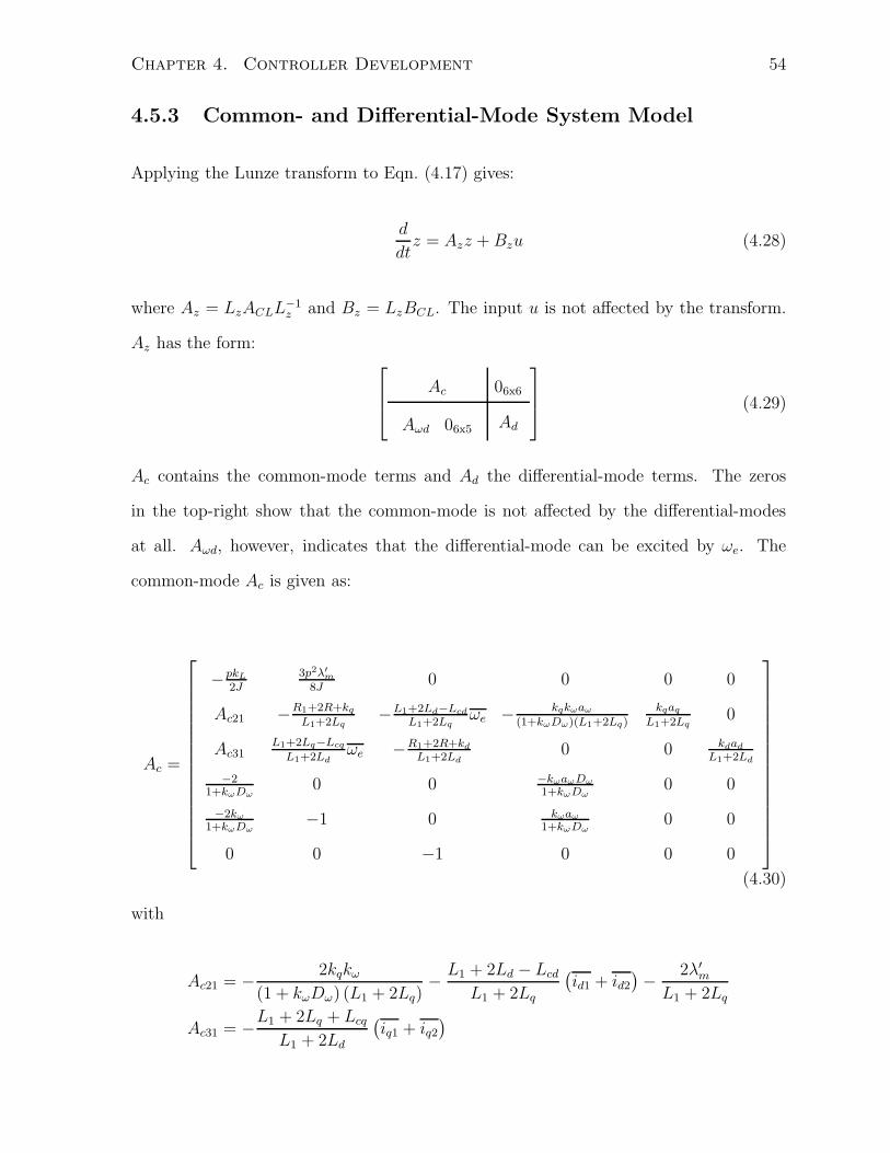
Chapter 4. Controller Development 54
4.5.3 Common- and Differential-Mode System Model
Applying the Lunze transform to Eqn. (4.17) gives:
d
dtz = Azz + Bzu (4.28)
where Az = LzACLL−1z and Bz = LzBCL. The input u is not affected by the transform.
Az has the form:
Ac 06x6
Aωd 06x5 Ad
(4.29)
Ac contains the common-mode terms and Ad the differential-mode terms. The zeros
in the top-right show that the common-mode is not affected by the differential-modes
at all. Aωd, however, indicates that the differential-mode can be excited by ωe. The
common-mode Ac is given as:
Ac =
−pkL
2J3p2λ′
m
8J0 0 0 0
Ac21 −R1+2R+kq
L1+2Lq−L1+2Ld−Lcd
L1+2Lqωe − kqkωaω
(1+kωDω)(L1+2Lq)kqaq
L1+2Lq0
Ac31L1+2Lq−Lcq
L1+2Ldωe −R1+2R+kd
L1+2Ld0 0 kdad
L1+2Ld
−21+kωDω
0 0 −kωaωDω
1+kωDω0 0
−2kω
1+kωDω−1 0 kωaω
1+kωDω0 0
0 0 −1 0 0 0
(4.30)
with
Ac21 = −2kqkω
(1 + kωDω) (L1 + 2Lq)−
L1 + 2Ld − Lcd
L1 + 2Lq
(
id1 + id2
)
−2λ′
m
L1 + 2Lq
Ac31 = −L1 + 2Lq + Lcq
L1 + 2Ld
(
iq1 + iq2)
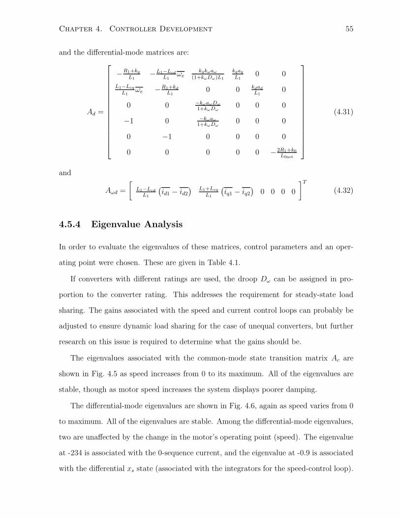
Chapter 4. Controller Development 55
and the differential-mode matrices are:
Ad =
−R1+kq
L1
−L1−Lcd
L1
ωekqkωaω
(1+kωDω)L1
kqaq
L1
0 0
L1−Lcq
L1
ωe −R1+kd
L1
0 0 kdad
L1
0
0 0 −kωaωDω
1+kωDω0 0 0
−1 0 −kωaω
1+kωDω0 0 0
0 −1 0 0 0 0
0 0 0 0 0 −2R1+k0
L0net
(4.31)
and
Aωd =
[
L1−Lcd
L1
(
id1 − id2
) L1+Lcq
L1
(
iq1 − iq2)
0 0 0 0
]T
(4.32)
4.5.4 Eigenvalue Analysis
In order to evaluate the eigenvalues of these matrices, control parameters and an oper-
ating point were chosen. These are given in Table 4.1.
If converters with different ratings are used, the droop Dω can be assigned in pro-
portion to the converter rating. This addresses the requirement for steady-state load
sharing. The gains associated with the speed and current control loops can probably be
adjusted to ensure dynamic load sharing for the case of unequal converters, but further
research on this issue is required to determine what the gains should be.
The eigenvalues associated with the common-mode state transition matrix Ac are
shown in Fig. 4.5 as speed increases from 0 to its maximum. All of the eigenvalues are
stable, though as motor speed increases the system displays poorer damping.
The differential-mode eigenvalues are shown in Fig. 4.6, again as speed varies from 0
to maximum. All of the eigenvalues are stable. Among the differential-mode eigenvalues,
two are unaffected by the change in the motor’s operating point (speed). The eigenvalue
at -234 is associated with the 0-sequence current, and the eigenvalue at -0.9 is associated
with the differential xs state (associated with the integrators for the speed-control loop).
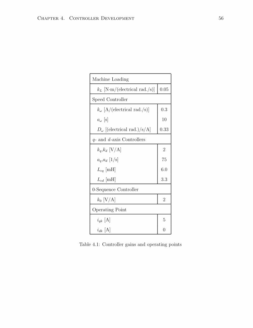
Chapter 4. Controller Development 56
Machine Loading
kL [N·m/(electrical rad./s)] 0.05
Speed Controller
kω [A/(electrical rad./s)] 0.3
aω [s] 10
Dω [(electrical rad.)/s/A] 0.33
q- and d -axis Controllers
kq,kd [V/A] 2
aq,ad [1/s] 75
Lcq [mH] 6.0
Lcd [mH] 3.3
0-Sequence Controller
k0 [V/A] 2
Operating Point
iqk [A] 5
idk [A] 0
Table 4.1: Controller gains and operating points

Chapter 4. Controller Development 57
−300 −250 −200 −150 −100 −50 0−400
−200
0
200
400
real
imag
Common−Mode Eigenvalues as e Varies 0 to max
−20 −18 −16 −14 −12 −10 −8 −6 −4 −2 0−50
0
50
real
imag
Eigenvalues Near the Origin
Figure 4.5: Common-Mode Eigenvalues
Based on Aωd, the differential-mode is only excited when there exists a difference in
operating point (id1 6= id2) between converter 1 and converter 2 and the speed changes.
Thus, for normal operation when the converters are sharing the load equally (assuming
their droops Dω are equal), the differential-mode eigenvalues are not excited.
In order to cancel the cross-coupling terms associated with Ac (Ac23 and Ac32), the
parameters Lcq and Lcd should be set as Lcd = L1+2Ld and Lcq = L1+2Lq. If these values
are chosen for Lcq and Lcd, however, the cross-coupling terms in the differential-mode
matrix Ad (Ad21 and Ad12) become significantly larger.
For the two-converter case the system remains stable, but this is an example where
optimizing the common-mode response is detrimental to the differential-mode stability.
If more converters were present, it might not be possible to cancel the cross-coupling
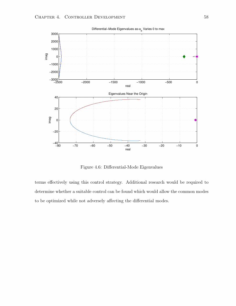
Chapter 4. Controller Development 58
−80 −70 −60 −50 −40 −30 −20 −10 0−40
−20
0
20
40
real
imag
Eigenvalues Near the Origin
−2500 −2000 −1500 −1000 −500 0−3000
−2000
−1000
0
1000
2000
3000
real
imag
Differential−Mode Eigenvalues as ωe Varies 0 to max
Figure 4.6: Differential-Mode Eigenvalues
terms effectively using this control strategy. Additional research would be required to
determine whether a suitable control can be found which would allow the common modes
to be optimized while not adversely affecting the differential modes.
Chapter 5
Results
5.1 Overview
This chapter validates the simulation model by comparing simulation and experimental
results. The system stability demonstrated in these results also supports the validity of
the eigenvalue analysis.
First, the machine model is validated against the experimental PMSM in Section 5.2.
Section 5.3 presents results for two different speed steps in order to confirm that the
converters share the load dynamically and in steady-state. This also demonstrates system
stability. In Section 5.4 demonstrates the system redundancy associated with the two-
converter arrangement.
5.2 Machine Model Validation
5.2.1 Open-Loop Response
The open-loop response was obtained using a single converter and applying steps to vtq1
and vtd1, the q- and d -axes voltages. Setting the voltages determines the converter’s
switching times directly.
59

Chapter 5. Results 60
These results are shown in Figs. 5.1a and 5.1b for the q-axis and in Figs. 5.2a and 5.2b
for the d -axis.
Due to the non-linear load characteristic, which was not modelled in detail, some
discrepancy exists between the experimental and simulation result for the vq test, but
overall the agreement is acceptable. The transient amplitudes are similar, as are the
waveform shapes of both iq and id for both tests.
A ripple-current is present on the experimental results for iq due to the trapezoidal
windings of the PMSM. For higher speed operation, the frequency of this ripple would
be increased and the system inductance provides more attenuation. For the id test no
ripple is present as the rotor is not turning.
There is an offset in the experimental results due to the voltage loss in the converter.
This is particularly noticeable in the id test due to the low voltage being requested, but
the machine dynamics—indicated by the time constant and magnitude of the current
change—are in good agreement.

Chapter 5. Results 61
0.4 0.45 0.5 0.55 0.6 0.65 0.7 0.75 0.8 0.85 0.9−5
−4
−3
−2
−1
0
1
2
3
4
5
Time [s]
iq
id
ωe
(a)
(b)
Figure 5.1: (a) Simulation and (b) experimental results for vq step from 15 to 20 V . ωe
is [20 rad/s/div] and iq and id are [5 A/div]. Experimental time is in ms.
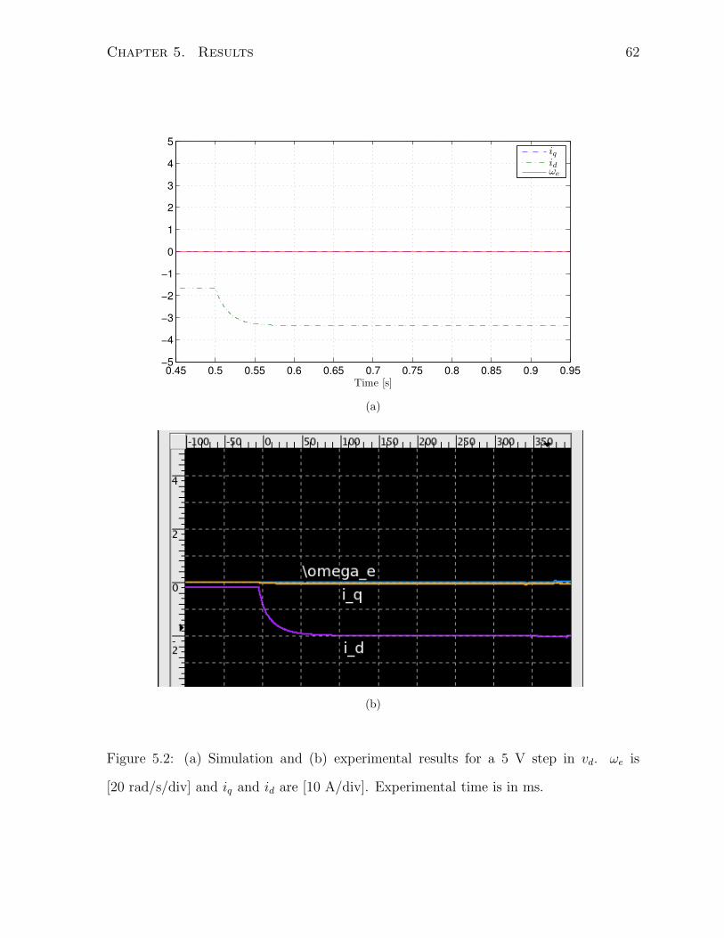
Chapter 5. Results 62
0.45 0.5 0.55 0.6 0.65 0.7 0.75 0.8 0.85 0.9 0.95−5
−4
−3
−2
−1
0
1
2
3
4
5
Time [s]
iqidωe
(a)
(b)
Figure 5.2: (a) Simulation and (b) experimental results for a 5 V step in vd. ωe is
[20 rad/s/div] and iq and id are [10 A/div]. Experimental time is in ms.

Chapter 5. Results 63
5.2.2 Closed-Loop Response
The closed-loop response is obtained by applying PI-controllers to the q-and d -axis cur-
rents. The q-axis current is stepped from 0.74 to 15.94 A (64% of rated), corresponding
to a step in Te from 0 to 20 N·m, while the d -axis current reference is fixed at 0 A. The
results are shown in Figs. 5.3a and 5.3b.
The simulation and experimental results are very similar, though there is some dy-
namic coupling between the q- and d -axes in the experimental setup which is not present
in the simulation. The rise and fall times are also similar, though the experimental
controller is slightly faster.

Chapter 5. Results 64
0.095 0.1 0.105 0.11 0.115 0.12 0.125 0.13 0.135 0.14 0.145−5
−4
−3
−2
−1
0
1
2
3
4
5
Time [s]
iqidωe
(a)
(b)
Figure 5.3: (a) Simulation and (b) experimental results for iqref step from 0.74 to 15.94
A. ωe is [20 rad/s/div] and iq and id are [5 A/div]. Experimental time is in ms.
Chapter 5. Results 65
5.3 System Response to Speed Steps
In order to validate the effectiveness of the control, two steps in the speed reference ω∗
e
were applied. The response of the qd and 0-sequence currents and the machine speed
was observed.
For each test, a series of 16 graphs, split into 4 figures, is shown. The first 8 graphs
show experimental results and the last 8 graphs replicate the first 8, but the simulation
results are shown. The first figure has 5 graphs: the first graph shows the applied speed
step and the motor speed and the next 4 graphs show the qd and 0-sequence currents
for both converters. The second figure, showing the sixth, seventh and eighth graphs,
shows the common- and differential-mode currents associated with the qd -axes and the
differential-mode 0-sequence current. These are derived from the current states described
in Eqn. (4.26).
The current references i∗qn were limited to 15 A for all tests, providing a nominal
maximum current of 30 A.
5.3.1 Low Speed Test
Figs. 5.4-5.7 show the low speed, moderate torque test. Current sharing between the
converters is excellent (first graph, Fig. 5.7), and at this low speed there is very little
cross-coupling between the q- and d -axes. The 0-sequence current is well controlled.
In the experimental setup, the speed step (first graph, Fig. 5.4) causes the speed
controller to saturate i∗q1,2 approximately 15 ms after the speed step is applied, and the
references remain in saturation until the motor speed reaches the new ω∗
e . The speed
overshoot is approximately 10% of the final value. Steady-state current changes from
approximately 4 A before the step to 8 A following the step (second and third graphs).
This corresponds to a load change from approximately 1/4- to 1/2-rated.
The ripple on the quadrature currents (second and third graph in Fig. 5.4) is due to

Chapter 5. Results 66
the machine’s trapezoidal windings.
Both experimentally and in simulation, the two converters respond essentially iden-
tically, excepting the switching ripple, and the cross-coupling in the simulation is very
similar to the experimental case. The agreement between the simulation and experiment
is excellent.

Chapter 5. Results 67
−0.1 0 0.1 0.2 0.3 0.4 0.5 0.6 0.7 0.8 0.9−140
−120
−100
−80
−60
Speed reference and motor speed [electrical rad/s]
−0.1 0 0.1 0.2 0.3 0.4 0.5 0.6 0.7 0.8 0.9−20
−10
0
10VSC1: Quadrature Currents [A]
−0.1 0 0.1 0.2 0.3 0.4 0.5 0.6 0.7 0.8 0.9−20
−10
0
10
Time [s]
VSC2: Quadrature Currents [A]
−0.1 0 0.1 0.2 0.3 0.4 0.5 0.6 0.7 0.8 0.9
−10
0
10
VSC1: Zero−Sequence Current [A]
−0.1 0 0.1 0.2 0.3 0.4 0.5 0.6 0.7 0.8 0.9
−10
0
10
VSC2: Zero−Sequence Current [A]
ωref
ω
iq1
id1
iq2
id2
i01
i02
Figure 5.4: Experimental: Response of VSC1 & VSC2 to a step in speed reference at
t = 0.0 s from 62 to 124 rad/s (electrical).
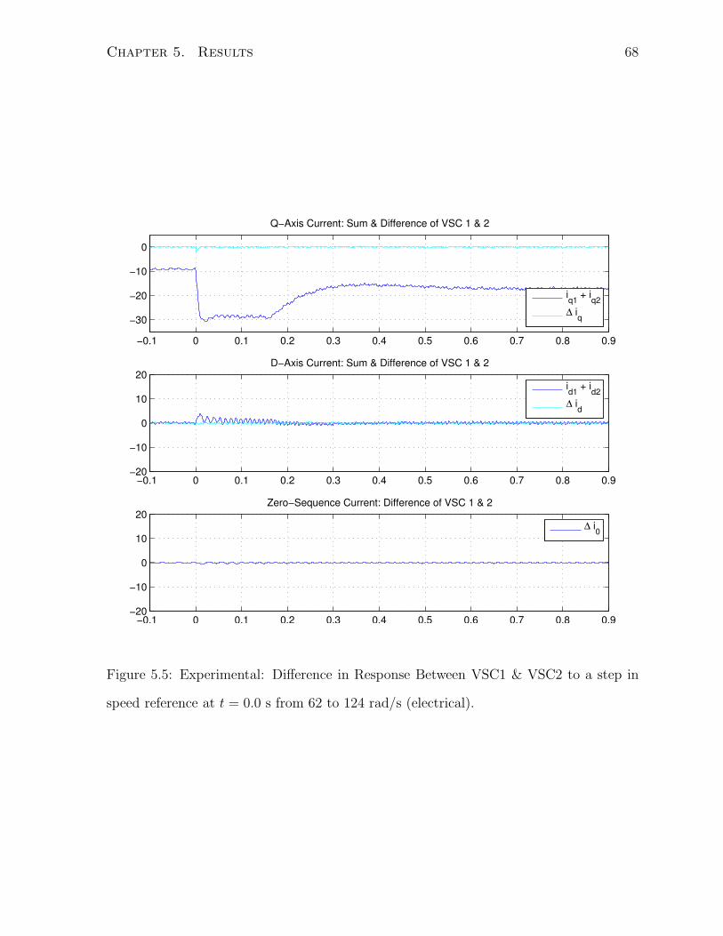
Chapter 5. Results 68
−0.1 0 0.1 0.2 0.3 0.4 0.5 0.6 0.7 0.8 0.9
−30
−20
−10
0
Q−Axis Current: Sum & Difference of VSC 1 & 2
−0.1 0 0.1 0.2 0.3 0.4 0.5 0.6 0.7 0.8 0.9−20
−10
0
10
20D−Axis Current: Sum & Difference of VSC 1 & 2
−0.1 0 0.1 0.2 0.3 0.4 0.5 0.6 0.7 0.8 0.9−20
−10
0
10
20Zero−Sequence Current: Difference of VSC 1 & 2
iq1
+ iq2
∆ iq
id1
+ id2
∆ id
∆ i0
Figure 5.5: Experimental: Difference in Response Between VSC1 & VSC2 to a step in
speed reference at t = 0.0 s from 62 to 124 rad/s (electrical).

Chapter 5. Results 69
0 0.1 0.2 0.3 0.4 0.5 0.6 0.7 0.8 0.9 1−140
−120
−100
−80
−60
Speed reference and motor speed [electrical rad/s]
0 0.1 0.2 0.3 0.4 0.5 0.6 0.7 0.8 0.9 1−20
−10
0
10VSC1: Quadrature Currents [A]
0 0.1 0.2 0.3 0.4 0.5 0.6 0.7 0.8 0.9 1−20
−10
0
10
Time [s]
VSC2: Quadrature Currents [A]
0 0.1 0.2 0.3 0.4 0.5 0.6 0.7 0.8 0.9 1
−10
0
10
VSC1: Zero−Sequence Current [A]
0 0.1 0.2 0.3 0.4 0.5 0.6 0.7 0.8 0.9 1
−10
0
10
VSC2: Zero−Sequence Current [A]
ωref
ω
iq1
id1
iq2
id2
i01
i02
Figure 5.6: Simulation: Response of VSC1 & VSC2 to a step in speed reference at
t = 0.1 s from 62 to 124 rad/s (electrical).

Chapter 5. Results 70
0 0.1 0.2 0.3 0.4 0.5 0.6 0.7 0.8 0.9 1
−30
−20
−10
0
Q−Axis Current: Sum & Difference of VSC 1 & 2
0 0.1 0.2 0.3 0.4 0.5 0.6 0.7 0.8 0.9 1−20
−10
0
10
20D−Axis Current: Sum & Difference of VSC 1 & 2
0 0.1 0.2 0.3 0.4 0.5 0.6 0.7 0.8 0.9 1−20
−10
0
10
20Zero−Sequence Current: Difference of VSC 1 & 2
iq1
+ iq2
∆ iq
id1
+ id2
∆ id
∆ i0
Figure 5.7: Simulation: Difference in Response Between VSC1 & VSC2 to a step in speed
reference at t = 0.1 s from 62 to 124 rad/s (electrical).

Chapter 5. Results 71
5.3.2 High Speed Test
Figures 5.8 to 5.11 show a speed step of 10% up to 2/3-rated speed (1133 rpm to
1333 rpm). The load is about 1/3-rated. The high- and low-speed tests are very similar.
For the high-speed case, the lighter load causes the speed controller’s response to be
faster, the overshoot to be slightly higher, and the saturation in the current to last for a
shorter time.
The most salient difference is the larger cross-coupling, where the spike on id reaches
approximately 50% of the spike in iq. The large cross-coupling partly results from the
choice of Lcq and Lcd, which were set to the machine inductances rather than the optimal
values determined from the eigenvalue analysis. The parallel converter arrangement
means an extra cross-coupling term, resulting from the other converter’s currents, is
present. The other converter’s currents are not measured, so this cannot be perfectly
cancelled. At low speed, this effect is negligible.
In Fig. 5.9, the currents iq1 and iq2 are marginally different, resulting in a non-zero
∆iq. This is caused by one of the controllers measuring a different speed than the other,
due to dropped encoder-counts. The droop on the speed reference causes the converters
to supply different iq currents, which is the desired operation.
In simulation, there is no significant difference between the converters’ response. For
the experimental case, the interface component variation account for the small difference
in response between converters (∆iq and ∆id on the first and second graph, Fig. 5.9).
Overall, the performance of the simulated system closely matched that of the exper-
imental system. The controllers caused the converters to share the load equally and the
system’s response was stable.
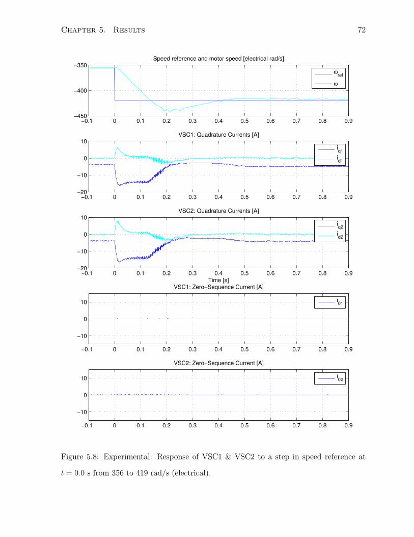
Chapter 5. Results 72
−0.1 0 0.1 0.2 0.3 0.4 0.5 0.6 0.7 0.8 0.9−450
−400
−350Speed reference and motor speed [electrical rad/s]
−0.1 0 0.1 0.2 0.3 0.4 0.5 0.6 0.7 0.8 0.9−20
−10
0
10VSC1: Quadrature Currents [A]
−0.1 0 0.1 0.2 0.3 0.4 0.5 0.6 0.7 0.8 0.9−20
−10
0
10
Time [s]
VSC2: Quadrature Currents [A]
−0.1 0 0.1 0.2 0.3 0.4 0.5 0.6 0.7 0.8 0.9
−10
0
10
VSC1: Zero−Sequence Current [A]
−0.1 0 0.1 0.2 0.3 0.4 0.5 0.6 0.7 0.8 0.9
−10
0
10
VSC2: Zero−Sequence Current [A]
ωref
ω
iq1
id1
iq2
id2
i01
i02
Figure 5.8: Experimental: Response of VSC1 & VSC2 to a step in speed reference at
t = 0.0 s from 356 to 419 rad/s (electrical).
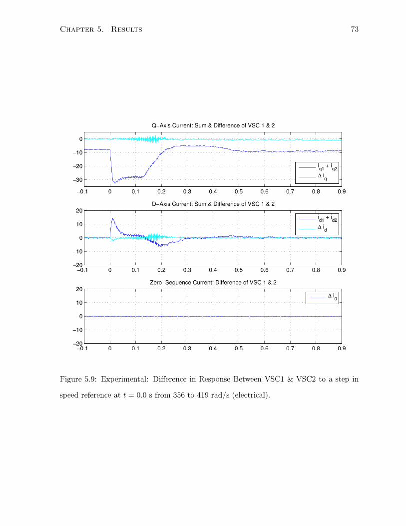
Chapter 5. Results 73
−0.1 0 0.1 0.2 0.3 0.4 0.5 0.6 0.7 0.8 0.9
−30
−20
−10
0
Q−Axis Current: Sum & Difference of VSC 1 & 2
−0.1 0 0.1 0.2 0.3 0.4 0.5 0.6 0.7 0.8 0.9−20
−10
0
10
20D−Axis Current: Sum & Difference of VSC 1 & 2
−0.1 0 0.1 0.2 0.3 0.4 0.5 0.6 0.7 0.8 0.9−20
−10
0
10
20Zero−Sequence Current: Difference of VSC 1 & 2
iq1
+ iq2
∆ iq
id1
+ id2
∆ id
∆ i0
Figure 5.9: Experimental: Difference in Response Between VSC1 & VSC2 to a step in
speed reference at t = 0.0 s from 356 to 419 rad/s (electrical).
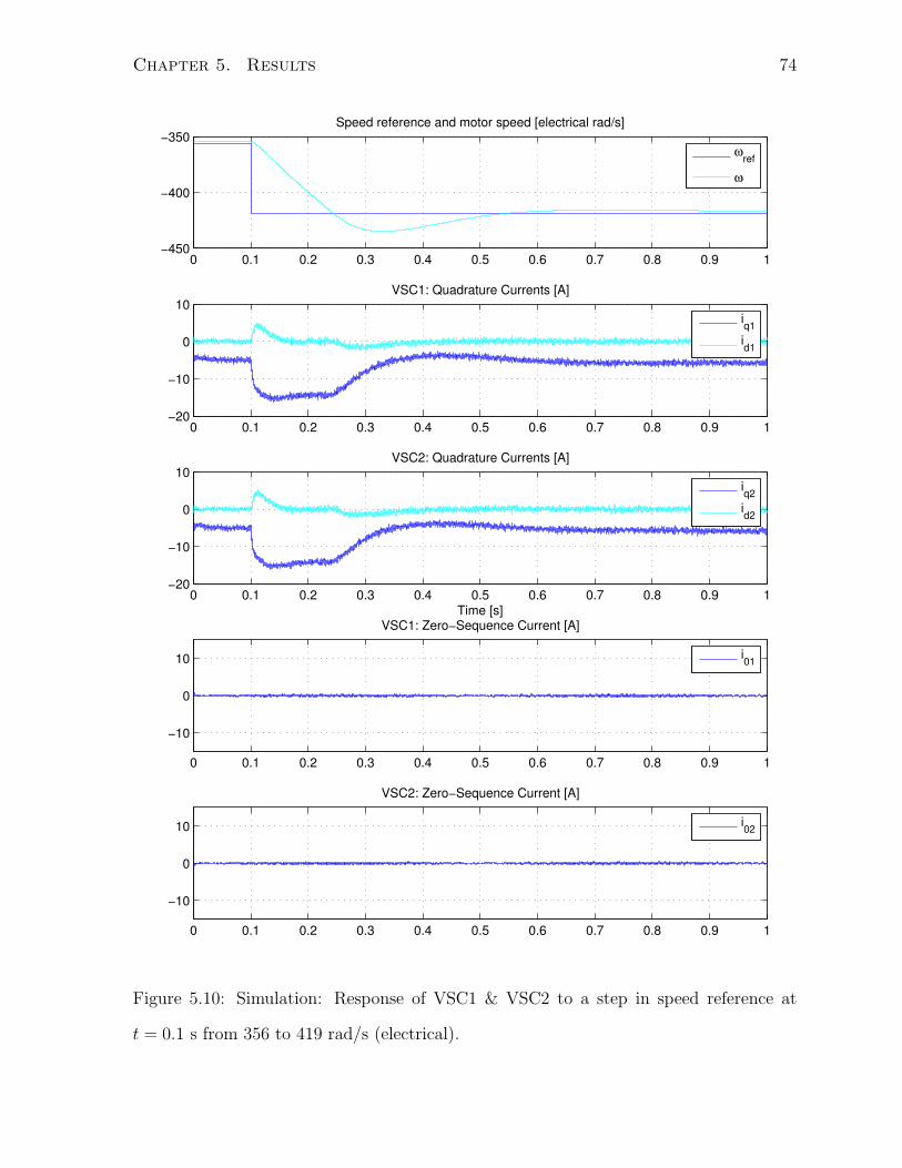
Chapter 5. Results 74
0 0.1 0.2 0.3 0.4 0.5 0.6 0.7 0.8 0.9 1−450
−400
−350Speed reference and motor speed [electrical rad/s]
0 0.1 0.2 0.3 0.4 0.5 0.6 0.7 0.8 0.9 1−20
−10
0
10VSC1: Quadrature Currents [A]
0 0.1 0.2 0.3 0.4 0.5 0.6 0.7 0.8 0.9 1−20
−10
0
10
Time [s]
VSC2: Quadrature Currents [A]
0 0.1 0.2 0.3 0.4 0.5 0.6 0.7 0.8 0.9 1
−10
0
10
VSC1: Zero−Sequence Current [A]
0 0.1 0.2 0.3 0.4 0.5 0.6 0.7 0.8 0.9 1
−10
0
10
VSC2: Zero−Sequence Current [A]
ωref
ω
iq1
id1
iq2
id2
i01
i02
Figure 5.10: Simulation: Response of VSC1 & VSC2 to a step in speed reference at
t = 0.1 s from 356 to 419 rad/s (electrical).

Chapter 5. Results 75
0 0.1 0.2 0.3 0.4 0.5 0.6 0.7 0.8 0.9 1
−30
−20
−10
0
Q−Axis Current: Sum & Difference of VSC 1 & 2
0 0.1 0.2 0.3 0.4 0.5 0.6 0.7 0.8 0.9 1−20
−10
0
10
20D−Axis Current: Sum & Difference of VSC 1 & 2
0 0.1 0.2 0.3 0.4 0.5 0.6 0.7 0.8 0.9 1−20
−10
0
10
20Zero−Sequence Current: Difference of VSC 1 & 2
iq1
+ iq2
∆ iq
id1
+ id2
∆ id
∆ i0
Figure 5.11: Simulation: Difference in Response Between VSC1 & VSC2 to a step in
speed reference at t = 0.1 s from 356 to 419 rad/s (electrical).
Chapter 5. Results 76
5.4 Loss of Converter
This section demonstrates the ability of the system to continue operating despite the loss
of one of the converters. In Fig. 5.12, the experimental system starts in steady-state at
approximately 1/3-rated speed. At t = 0.2 converter 2’s gating was shut off to emulate
the loss of that controller.
Fig. 5.13 shows a simulation of the same case. The response is almost identical to the
response of the laboratory system, indicating that the simulation results are reliable for
this type of test.
As a result of the loss of gating, a speed dip of less than 10% occurs. The motor settles
to a new steady-state speed in approximately 800 ms. This new speed is slightly less
than the original speed as a result of the droop Dω. The plots of the quadrature currents
show that until converter 2 lost its gating signals the load was shared equally. At that
point, converter 2 no longer provides q-axis current and converter 1 begins to increase iq1
to compensate, as the same net iq is required to maintain the motor’s speed. Also note
that at t = 0.2 s. when converter 2 is lost, converter 1’s current immediately jumps to
the net iq as a result of the requirement for continuity in the currents resulting from the
machine inductance. The q-axis controller quickly returns iq1 to the pre-transient state,
which causes cross-coupling with the d -axis, resulting in a transient in d -axis current
also.
The increase in iq1 is driven by speed control loop whose error signal is the differ-
ence between the motor speed and its reference. As the motor dynamics are slow, this
compensator also reacts slowly.
The 0-sequence current is initially regulated to zero and the loss of one of the con-
verters does not affect its regulation, although the 0-sequence switching ripple is reduced
because the applied voltage v0 is smaller. Note that a closed-loop path for 0-sequence
current still exists through the disabled converter 2.
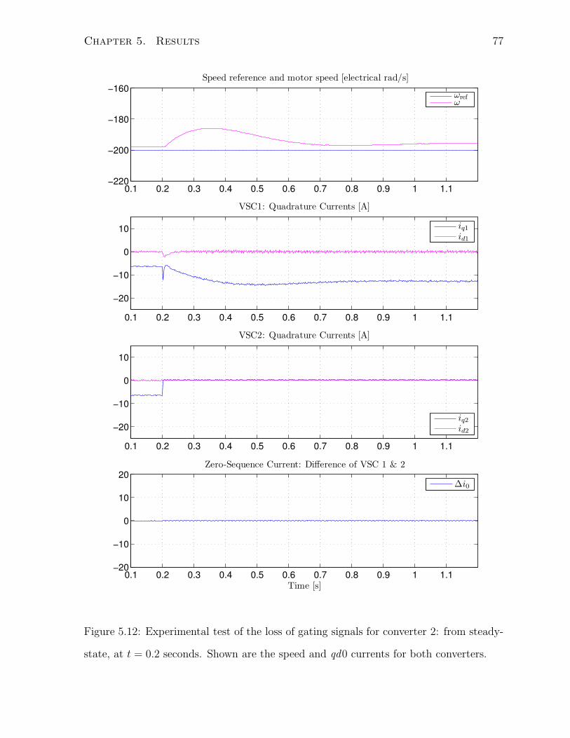
Chapter 5. Results 77
0.1 0.2 0.3 0.4 0.5 0.6 0.7 0.8 0.9 1 1.1−220
−200
−180
−160Speed reference and motor speed [electrical rad/s]
ωref
ω
0.1 0.2 0.3 0.4 0.5 0.6 0.7 0.8 0.9 1 1.1
−20
−10
0
10
VSC1: Quadrature Currents [A]
iq1id1
0.1 0.2 0.3 0.4 0.5 0.6 0.7 0.8 0.9 1 1.1
−20
−10
0
10
VSC2: Quadrature Currents [A]
iq2id2
0.1 0.2 0.3 0.4 0.5 0.6 0.7 0.8 0.9 1 1.1−20
−10
0
10
20
Time [s]
Zero-Sequence Current: Difference of VSC 1 & 2
∆i0
Figure 5.12: Experimental test of the loss of gating signals for converter 2: from steady-
state, at t = 0.2 seconds. Shown are the speed and qd0 currents for both converters.
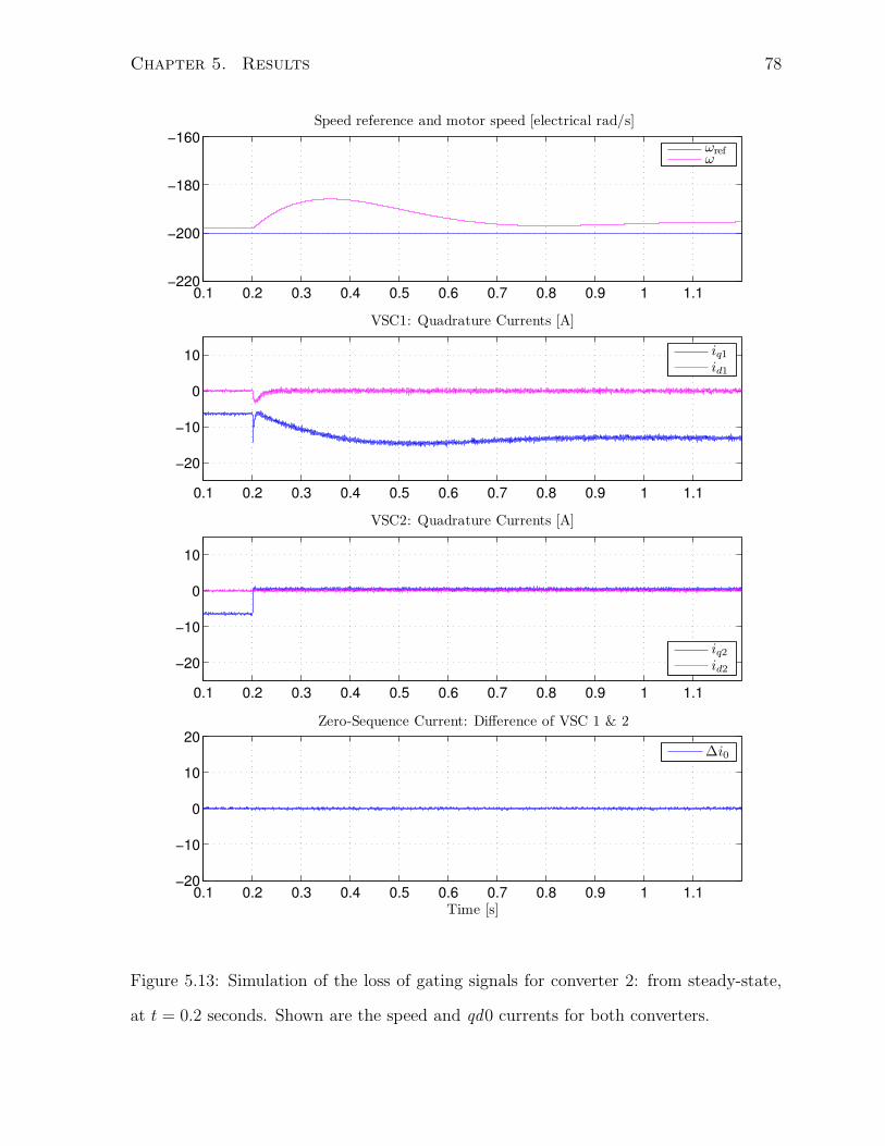
Chapter 5. Results 78
0.1 0.2 0.3 0.4 0.5 0.6 0.7 0.8 0.9 1 1.1−220
−200
−180
−160Speed reference and motor speed [electrical rad/s]
0.1 0.2 0.3 0.4 0.5 0.6 0.7 0.8 0.9 1 1.1
−20
−10
0
10
VSC1: Quadrature Currents [A]
0.1 0.2 0.3 0.4 0.5 0.6 0.7 0.8 0.9 1 1.1
−20
−10
0
10
VSC2: Quadrature Currents [A]
0.1 0.2 0.3 0.4 0.5 0.6 0.7 0.8 0.9 1 1.1−20
−10
0
10
20
Time [s]
Zero-Sequence Current: Difference of VSC 1 & 2
ωref
ω
iq1id1
iq2id2
∆i0
Figure 5.13: Simulation of the loss of gating signals for converter 2: from steady-state,
at t = 0.2 seconds. Shown are the speed and qd0 currents for both converters.

Chapter 6
Conclusions
A parallel motor drive consisting of two converters directly connected to a common
dc source and a single PMSM was developed. The converters are controlled indepen-
dently without converter inter-communication and do not depend on a master/slave
arrangement.
A laboratory model of the system was developed. The system is described with a
particular emphasis on the implications of the transition to the two-converter drive from
the single-converter drive. The 0-sequence switching ripple was characterized and a new
model describing the circulating 0-sequence current was identified.
A new linearized state-space model of the system was developed using the rotating
qd0 reference frame aligned with the PMSM’s rotor. This mathematical formulation is
well-suited to the study of multi-converter motor drives.
The transformation also resulted in the 0-sequence components being decoupled from
the rest of the system. The qd currents are coupled through the motor and each converter
is affected by the other converter’s control voltages.
To ensure steady-state load sharing, a new drooped PI speed control scheme controls
the converters’ q-axis current references. The control exploits the decoupled nature of
the qd and 0-sequence quantities and uses PI controllers to control qd current loops. The
79

Chapter 6. Conclusions 80
controllers do not communicate and only depend on the machine position and the locally
available current and voltage information. The stability of the closed-loop system was
confirmed using an eigenvalue analysis.
The system was simulated in MATLAB/Simulink and the simulation was validated
against the laboratory model by comparing the open- and closed-loop responses and
applying a step in speed. The usefulness of the parallel converter arrangement was
demonstrated through a test wherein one of the converters stopped gating and the system
continued to operate.
Future research in the area of parallel motor drives should focus on the extension of
the two converter system presented here to the case of N converters. This will likely
necessitate the investigation of a new control method capable of stabilizing the larger
system and holds significant potential for providing more cost-effective and reliable drive
structures.
Another area for future work is to run the system sensorless (without the encoder),
possibly using the voltage at the PCC to determine the machine position.

Bibliography
[1] T. Kawabata and S. Higashino, “Parallel operation of voltage source inverters,”
Industry Applications, IEEE Transactions on, vol. 24, no. 2, pp. 281–287, Mar/Apr
1988.
[2] H. Van Der Broeck and U. Boeke, “A simple method for parallel operation of in-
verters,” Telecommunications Energy Conference, 1998. INTELEC. Twentieth In-
ternational, pp. 143–150, 1998.
[3] J. Tan, H. Lin, J. Zhang, and J. Ying, “A novel load sharing control technique for
paralleled inverters,” Power Electronics Specialist Conference, 2003. PESC ’03. 34th
Annual, vol. 3, pp. 1432–1437, 15-19 June 2003.
[4] U. Borup, F. Blaabjerg, and P. Enjeti, “Sharing of nonlinear load in parallel-
connected three-phase converters,” vol. 37, no. 6, pp. 1817–1823, Nov/Dec 2001.
[5] A. Tuladhar, H. Jin, T. Unger, and K. Mauch, “Parallel operation of single phase
inverter modules with no control interconnections,” Applied Power Electronics Con-
ference and Exposition, 1997. APEC ’97 Conference Proceedings 1997., Twelfth An-
nual, vol. 1, pp. 94–100, 23-27 Feb 1997.
[6] Y. Byun, T. Koo, K. Joe, E. Kimb, J. Seo, and D. Kim, “Parallel operation of three-
phase UPS inverters by wireless load sharing control,” Telecommunications Energy
Conference, 2000. INTELEC. Twenty-second International, pp. 526–532, 2000.
81
Bibliography 82
[7] C. Sao and P. Lehn, “Intentional islanded operation of converter fed microgrids,”
Power Engineering Society General Meeting, 2006. IEEE, p. 6 pp., June 2006.
[8] C. Sao and P. Lehn, “Paper TPWRS-00778-2006: Control and power management of
converter fed microgrids,” To be published in IEEE Transactions on Power Systems.
[9] C.-T. Pan and Y.-H. Liao, “Modeling and coordinate control of circulating currents
in parallel three-phase boost rectifiers,” vol. 54, no. 2, pp. 825–838, April 2007.
[10] S. Mazumder, “Continuous and discrete variable-structure controls for parallel three-
phase boost rectifier,” vol. 52, no. 2, pp. 340–354, April 2005.
[11] K. Matsui, Y. Murai, M. Watanabe, M. Kaneko, and F. Ueda, “A pulsewidth-
modulated inverter with parallel connected transistors using current-sharing reac-
tors,” Power Electronics, IEEE Transactions on, vol. 8, no. 2, pp. 186–191, Apr
1993.
[12] T. Halkosaari, “Speed sensorless vector control of a redundant permanent magnet
wind power generator,” Industrial Electronics, 2007. ISIE 2007. IEEE International
Symposium on, pp. 2595–2600, June 2007.
[13] B. Shi and G. Venkataramanan, “Parallel operation of voltage source inverters with
minimal intermodule reactors,” Industry Applications Conference, 2004. 39th IAS
Annual Meeting., vol. 1, pp. 156–162, 3-7 Oct. 2004.
[14] Z. Ye, D. Boroyevich, J.-Y. Choi, and F. Lee, “Control of circulating current in two
parallel three-phase boost rectifiers,” vol. 17, no. 5, pp. 609–615, Sep 2002.
[15] J. Matakas, L. and W. Kaiser, “Low harmonics, decoupled histeresis type current
control of a multiconverter consisting of a parallel transformerless connection of
vsc converters,” Industry Applications Conference, 1997. Thirty-Second IAS Annual
Bibliography 83
Meeting, IAS ’97., Conference Record of the 1997 IEEE, vol. 2, pp. 1633–1640, 5-9
Oct 1997.
[16] T.-P. Chen, “Circulating zero-sequence current control of parallel three-phase invert-
ers,” Electric Power Applications, IEE Proceedings -, vol. 153, no. 2, pp. 282–288,
March 2006.
[17] R. Cuzner, D. Nowak, A. Bendre, G. Oriti, and A. Julian, “Mitigating circulating
common-mode currents between parallel soft-switched drive systems,” vol. 43, no. 5,
pp. 1284–1294, Sept.-Oct. 2007.
[18] J. Hwang, P. Lehn, and M. Winkelnkemper, “Control of grid connected ac-dc con-
verters with minimized dc link capacitance under unbalanced grid voltage condi-
tion,” Power Electronics and Applications, 2007 European Conference on, pp. 1–10,
Sept. 2007.
[19] P. C. Krause and O. Wasynczuk, Electromechanical Motion Devices. Toronto:
McGraw-Hill, 1989.
[20] S. Nasar and I. Boldea, Electric Machines Dynamics and Control. Ann Arbor,
Michigan: CRC Press, 1993.
[21] A. Garg, D. Perreault, and G. Verghese, “Feedback control of paralleled symmetric
systems, with applications to nonlinear dynamics of paralleled power converters,”
vol. 5, 1999, pp. 192–197 vol.5.
[22] J. Lunze, Feedback Control of Large-Scale Systems. Toronto: Prentice Hall, 1992.
[23] K. C. Sao, “Dynamic control and power management of converter fed microgrids,”
Ph.D. dissertation, University of Toronto, Toronto, Ontario, 2007.
[24] Allen-Bradley Bulletin 845F Incremental Encoders.

Appendix A
Motor Details
Most machine parameters are listed in Fig. A.1, however some tests indicated discrepan-
cies between the datasheet and actual values.
Magnet Strength
The strength of the magnetic field, denoted λ′
m [V/s] with the ′ indicating a quantity
referred to the stator side, can be determined in several ways. From the datasheet rated
values and (3.11):
λ′
m =4Te
3Piqs
(A.1)
which gives λ′
m = 0.281. Using the same relation and measuring the torque gave λ′
m =
0.278.
Alternatively, based on (3.9): if ωe is large then setting id = 0 using vdref = 0,
measuring iq, and applying a known vq allows λ′
m to be determined according to:
λ′
m =vq − Rsiq − Lq
diqdt
ωe(A.2)
In all cases the result was close to the datasheet value.
84
Appendix A. Motor Details 85
Resistance
The system resistances were measured with the laboratory milliohm meter. The ma-
chine’s stator resistance was measured as 0.354 Ωl−l, giving R = 0.177 Ω. The line
resistance from converter terminal to motor terminal was measured at about 0.1 Ω.
Inductance
As only one value for inductance is given on the motor’s datasheet: 16.3 mHl−l, the
machine was assumed to have a non-salient rotor (with surface-mounted magnets). How-
ever, after determining that the cross-coupling terms did not correspond well with the
predicted values, additional tests to determine the real machine inductance were per-
formed. As there seemed to be rotor saliency (that is, Lq 6= Ld, normally because the
magnets are embedded in the rotor, resulting in a change in the cross-section of the mag-
netic material), tests were performed along both the q- and d -axes. The first method
was to apply a step on the q- axis voltage under a locked-rotor condition. The second
method involved operating at high speed and determining the inductance to eliminate
the cross-coupling terms.
For the first method, a large clamp was attached to the shaft to physically lock the
rotor, setting ωe = 0. As a result, any changes are associated with the electrical circuit.
By applying a voltage vd and measuring the slope of the current, the inductance can be
approximated based on the voltage applied and the approximate slope of the current at
t = 0 (the instant when voltage is applied):
Ld ≈ vd∆i(0)
∆t(0)(A.3)
The same process can be repeated to determine Lq.
The second method involves operating with ω large and varying Ld (Lq) to cancel the
cross-coupling terms.

Appendix A. Motor Details 86
Pin Function
A Channel A Output
B Channel B Output
C Channel C Output
D DC+ Input
E — (internal connection to D)
F DC Return
G Case Ground
H Channel A Output
I Channel B Output
J Channel Z Output
Table A.1: 10-pin encoder pinout
Averaged together, these results gave the true machine inductances: Ld = 3.3 mH
and Lq = 6.0 mH .
Encoder
A 4000-pulse encoder is fixed to the rotor of the PMSM. No information specific to this
particular encoder was available, but the encoder uses the standard 10-pin layout of
Table A.1[24].
The encoder should be supplied with approximately 10 V. Channels A and B are the
counters while channel Z is the reset pulse. The encoder output was extremely noisy and
a large common-mode filter was place on the encoder’s channel Z output.
At high speeds, the encoder’s reset pulse is small enough that VSC2’s controller
was unable to consistently recognize the reset pulse, rendering the speed measurement
unreliable. Thus, no high speed tests were performed because controller 2 could not

Appendix A. Motor Details 87
operate.
Controller 2 was unable to read positive ωe, so only positive-speed tests were per-
formed in the laboratory. This is likely an FPGA issue.
Appendix A. Motor Details 88
Kollmorgen GOLDLIN
KOLLMORGEN • Radford, Virginia • 1-800-77 SERVO
80x PERFORMANCE DATA
36
B-802-A B-802-B B-802-C B-804-A
BE-802-A BE-802-B BE-802-C BE-804-A
M-803-A M-803-B M-803-C M-805-A
ME-803-A ME-803-B ME-803-C ME-805-A
Parameters Symbols Units EB-802-A EB-802-B EB-802-C EB-804-A
Horsepower HP Rated HP 10.6 13.6 8.2 14.5
Kilowatts kW Rated kW 7.9 10.1 6.1 10.8
Speed at Rated Power N Rated RPM 2000 2750 1600 1500
Max Operating Speed N Max RPM 2000 2750 1600 1500
Continuous Torque (stall) Tc lb-ft 31.0 30.0 30.0 58.0
at 40ºC N-m 42.0 40.7 40.7 78.6
Continuous Torque (stall) Tc lb-ft 32.9 31.8 31.8 61.5
at 25ºC N-m 44.6 43.1 43.1 83.4
Continuous Line Current Ic Amps RMS 24.9 32.4 18.9 35.0
Peak Torque Tp lb-ft 96.0 95.3 95.3 171.0
N-m 130.0 129.0 129.0 232.0
Peak Line Current Ip Amps RMS 81.0 108.0 60.0 109
Max Theoretical
Acceleration (B, BE, EB-80x) Z rad / sec2 26700 26500 26500 27600
(M, ME-80x) Z rad / sec2 3710 3680 3680 3870
Torque Sensitivity (stall) ±10% Kt lb-ft / Amp RMS 1.25 0.93 1.59 1.66
N-m / Amp RMS 1.69 1.26 2.16 2.25
Back EMF (line-to-line) ±10% Kb VRMS / kRPM 102.0 76.0 130.0 136.0
Max line-to-line Volts VMax Volts RMS 250 250 250 250
DC Res at 25ºC
(line-to-line) ±10% Rm Ohms 0.361 0.200 0.568 0.230
Inductance (line-to-line) ±30% Lm mh 16.3 9.4 25.7 13.0
Rotor Inertia (B, BE, EB-80x) Jm lb-ft-sec2 0.00360 0.00360 0.00360 0.00620
kg-m2 0.00488 0.00488 0.00488 0.00840
(M, ME-80x) lb-ft-sec2 0.0259 0.0259 0.0259 0.04415
kg-m2 0.0352 0.0352 0.0352 0.05990
Weight (B, BE-80x) Wt lb 79 79 79 112
kg 36 36 36 50.6
(M, ME-80x) Wt lb 96 96 96 138
kg 43.7 43.7 43.7 62.8
(EB-80x) Wt lb 79 79 79 112
kg 36 36 36 50.6
Static Friction Tf lb-ft 0.47 0.47 0.47 0.67
N-m 0.64 0.64 0.64 0.91
Thermal Time Constant
(B, BE, M, ME-80x) TCT Min 40 40 40 48
Thermal Time Constant
(EB-80x) TCT Min .60 .60 .60 .70
Viscous Damping Z Source Fi lb-ft / kRPM 0.175 0.175 0.175 0.221
N-m / kRPM 0.237 0.237 0.237 0.300
Motor Constant at 25ºC Km lb-ft / W 1.79 1.79 1.82 3.00
N-m / W 2.43 2.43 2.47 4.06
Thermal Resistance at stall Rth ºC / Watt 0.23 0.24 0.25 0.18
Number of Poles 6 6 6 6
Figure A.1: Motor Information for Kollmorgen Goldline M-803-A.
Appendix B
Implementation Issues
B.1 Common-Mode Signal Filters
In the experimental setup when both converters are switching, a significant amount of
noise is present on the input and output channels for converter 2’s controller. This noise
is not present on converter 1’s controller, and seems to form a closed-loop through the
computer. The anti-aliasing filter and input filters at the computer’s terminal block, each
of which is designed to attenuate only differential-mode signals, has little or no effect on
this signal, suggesting that this is a common-mode problem. The input channels are
all differential-mode inputs, so it is unclear why the common-mode is causing such a
problem, and the source for this noise is not known.
To mitigate the noise, a common-mode choke was added to each of the input and
output signals. As the desired signal is entirely differential-mode, this should have a
negligible effect on the phase and magnitude of the measured signal, but it provides very
high-impedance to the problematic common-mode noise. The chokes were constructed
from magnetic toroids and consist of approximately 20 turns each.
89

Appendix B. Implementation Issues 90
B.2 Simulation Stability
In order to preserve system stability during simulation, resistors are required in series
with the EMI capacitors at the PCC. An acceptable value is 10 Ω, but a smaller value
such as 1 Ω results in extremely large currents occurring in simulation. The value should
be as small as possible as the EMI capacitors have an impedance of about 5 Ω at the
switching frequency.
B.3 Time-Step Size and Solver Choice
In order to attain accurate results for the common-mode (0-sequence) current in partic-
ular, a small time-step is required. For most simulations, 2 µs characterizes the process
well, but the dynamics of the common-mode current does not exhibit periodicity and
should not be considered reliable. To get an accurate simulation of the common-mode
current, a time-step of 1 µs, or possibly even smaller, must be used.
The solver chosen is a stiff, fixed time-step solver: ode2. Variable time-step solvers
tended to take too long and require too small of a minimum time-step.

Appendix C
RT-Linux Control Code
// d e s c r i p t i o n :// This c o n t r o l l e r has been deve loped to con t r o l the PMSM. The code// was o r i g i n a l l y modi f ied by Dale Dolan with the s o l e goa l to act as a// torque c o n t r o l l e r ( us ing current r e f e r en c e on ly ) .//// Modi f i ca t ion s were made in the summer & f a l l o f 2008 by Danny Fingas// in order to t e s t the v a l i d i t y o f a MATLAB model o f a system// incorpora t i ng the PMSM. Code s p e c i f i c to the torque sensor was// removed .//// Or ig ina l ( c ) 2003 Hung Shyu//// r tce boo lean param gat ing on f a l s e ”Gating on . Choose ONLY ONE OF:”// r t c e l i n e// r tce boo lean param c l a s s i c a l f a l s e ”Open−Loop S inu so i da l
Voltage Source ”// r tce boo lean param vo l t a g e c o n t r o l f a l s e ”q−d Voltage Contro l ”// r tce boo lean param to r que c on t r o l f a l s e ”Manual Torque and Id
Re fe r ence s”// r tce boo lean param spe ed con t r o l t rue ”Use Drooped Speed Contro l
to s e t I q r e f ”
// r t c e l i n e// r t c e s c a l a r me t e r Thetadisp ”%0.2 f deg . ” ”Rotor Angle ( theta )
[ deg . ] ”// r t c e s c a l a r me t e r a vg e l e c s p e ed ”%0.2 f rad” ”Average Elec . Speed [
rade / s ] ”// r t c e s c a l a r me t e r w f i l t e r e d d i s p ”%0.2 f rad” ” e l e c . f r e q . (
f i l t e r e d ) [ rade / s ] ”// r t c e s c a l a r me t e r w un f i l t e r edd i s p ”%0.2 f rad” ” e l e c . f r e q . [
rade / s ] ”
// r t c e l i n e// r t c e s c a l a r me t e r v DCdisp ”%0.1 f V dc” ”dc−l i n k Voltage ”// r t c e s c a l a r me t e r Vl imi td i sp ”%0.2 f ” ”Vlimit ”
91
Appendix C. RT-Linux Control Code 92
// r t c e s c a l a r me t e r Vl eng th co r r e c t ed ”%0.2 f ” ”Vleng th co r r e c t ed ”
// r t c e s c a l a r me t e r Vlengthdisp ”%0.2 f ” ”Vlength”// r t c e s c a l a r me t e r I q r e f d i s p ”%0.2 f ” ” I q r e f ( i f app l i c ab l e ) ”
// rtce new column
// r t c e s c a l a r s l i d e r LPCO 40 .0 0 .1 100 .0 ”LPF f r e q . [ Hz ] for
speed ”// r t c e s c a l a r pa r am an g l e d e l t a r e f 42 .0 −180 +179 ”Angle [ Degree ] ”// r t c e s c a l a r pa r am lambda mag 0 .272 −1.0 1 . 0 ”lambda mag
. ”// r t c e s c a l a r pa r am Lq 0 .0040 −0.015 0 .015 ”Lq”// r t c e s c a l a r pa r am Ld 0 .0033 −0.015 0 .015 ”Ld”
// r t c e l i n e// r t c e s c a l a r s l i d e r f r equency 0 0 6 ”Open−loop Volt . Freq [ Hz ] ”// r t c e s c a l a r s l i d e r ma 0 0 1 .0 ”Open−loop ma”// r t c e s c a l a r s l i d e r ad ju s t ang l e 0 .000 −179.000 180 .000 ” ad jus t ang le
[ deg r e e s ] ”// r t c e l i n e// r t c e s c a l a r pa r am Vqref 0 . 0 −130.0 130 .0 ”Vqref (q−d Voltage
Contro l ) ”// r t c e s c a l a r pa r am Vdref 0 . 0 −130.0 130 .0 ”Vdref (q−d Voltage
Contro l ) ”// r t c e l i n e// r t c e s c a l a r pa r am Tref 0 . 0 −20.0 40 .000 ”Tq Ref . [N∗m] (Manual Ref . )
”// r t c e s c a l a r pa r am Idrefmanual 0 . 0 −30.0 30 .000 ” I d r e f (Manual
Reference ) ”
// rtce new column// r t c e s c a l a r pa r am wre fSet −157.1 −628.3 628 .3 ”Speed Reference [
rade / s ] ”// r t c e s c a l a r me t e r wre fDisp lay ”%0.2 f rade / s ” ”Tracked Speed”// r t c e s c a l a r pa r am operat iona lChangeDel ta 20 .0 −600 600 ”Step S i z e [
rade / s ] for Op. Change”// r t c e s c a l a r pa r am I 0 r e f s e t 0 . 0 −20.0 20 .0 ”Zero−Sequence Current
Reference [A] ”// r t c e s c a l a r pa r am I d r e f s e t 0 . 0 −20.0 20 .0 ”D−Axis Current
Reference [A] ”// r t c e s c a l a r s l i d e r Kpq 2 .0 0 . 0 10 .0 ”q−ax i s Propo r t i ona l Gain
Kpq ”// r t c e s c a l a r s l i d e r Kiq 150 .0 0 . 0 600 .0 ”q−ax i s I n t e g r a l Gain
Kiq ”// r t c e s c a l a r s l i d e r Kpd 2 .0 0 . 0 10 .0 ”d−ax i s Propo r t i ona l Gain
Kpd ”// r t c e s c a l a r s l i d e r Kid 150 .0 0 . 0 600 .0 ”d−ax i s I n t e g r a l Gain
Kid ”// r t c e s c a l a r s l i d e r Kpzero 2 .0 0 . 0 10 .0 ”Zero−Sequence
Propo r t i ona l Gain Kpzero”// r t c e s c a l a r s l i d e r Kpw 0 .3 0 .01 2 .0 ”Speed Loop Propo r t i ona l
Gain Kpw ”// r t c e s c a l a r s l i d e r aw 10 .0 0 . 1 100 .0 ”Speed Loop Zero

Appendix C. RT-Linux Control Code 93
Placement aw”// r t c e s c a l a r s l i d e r Dw 0.33 0 .0 2 . 0 ”Speed Droop”
#de f i n e VERBOSE // f o r output o f PRINTF#inc lude ” r tce module . h”#inc lude ” r t c e c o n t r o l . h”#inc lude ”acromag . h”#inc lude ” . . / fpga /pwm. h”
// inc lude automat i ca l l y c r ea ted parameter d e f i n i t i o n s#inc lude ” pa r s e r output . h”
// get the shared memory support f o r parameter exchange#inc lude ” rtce shared mem param . h”#inc lude ” rt math . h”#inc lude ” math too l s . h”#inc lude ” c o n t r o l t o o l s . h”
s t a t i c f l o a t s i g n a l [ 6 4 ] ;#de f i n e SIGNAL( i ) s i g n a l [ i ]
double s e c o nd o r d e r l p f ( double x , double ∗x0 , double ∗x1 ,double ∗y0 , double ∗y1 , double Q, double wc , double Tsample ) ;
double f i r s t o r d e r l p f ( double x , double ∗x0 , double ∗y0 , double wc ,double Tsample ) ;
s t a t i c i n t r tce create sharedmem ( void ) i n t r e s u l t= r t c e c r e a t e s ha r edmem fo r th i s numbe r o f i t ems (
RTCE NUM SCALAR PARAMS,RTCE NUM BOOLEAN PARAMS,RTCE NUM SCALAR METERS,RTCE NUM SCALAR SLIDERS ) ;
// only the cont ro l−module may r e s e t the s e l e c t−index on startup ,// i f the u s e r i n t e r f a c e r e s e t s t h i s index on startup ,// i t changes the parameter that might be used by a running
c o n t r o l l e ri f ( ( r e s u l t==0) && (RTCE NUM CONFIRM PARAMS!=0) )
∗ r t c e c t r l memo r y b l o c k s e l e c t i n d e x = 0 ;return r e s u l t ;
// −−−−−−−−−−−−−−−−−−−−−−−−−−−−−−−−−−−−−−−−−−−−−−−−−−−−−−−// module s e c t i o n//// t h i s c o n t r o l l e r can be bu i l t as a module// in t h i s case only t h i s f i l e needs to be recompi led// −−−−−−−−−−−−−−−−−−−−−−−−−−−−−−−−−−−−−−−−−−−−−−−−−−−−−−−#i f d e f MODULE// ATTENTION: no f l o a t i n g po int in the s e f unc t i o n s ! ! ! !i n t in i t modu l e ( void )
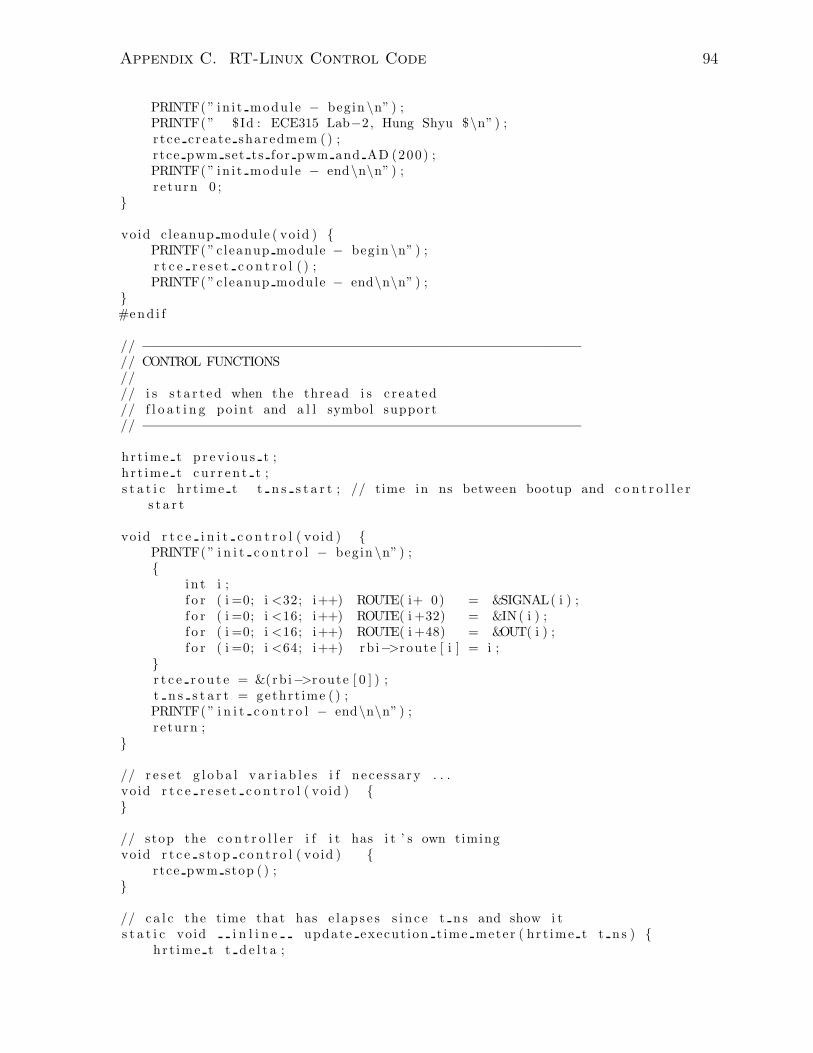
Appendix C. RT-Linux Control Code 94
PRINTF(” in i t modu l e − begin \n” ) ;PRINTF(” $Id : ECE315 Lab−2, Hung Shyu $\n” ) ;r tce create sharedmem ( ) ;rtce pwm set ts for pwm and AD (200) ;PRINTF(” in i t modu l e − end\n\n” ) ;r e turn 0 ;
void cleanup module ( void ) PRINTF(” cleanup module − begin \n” ) ;r t c e r e s e t c o n t r o l ( ) ;PRINTF(” cleanup module − end\n\n” ) ;
#end i f
// −−−−−−−−−−−−−−−−−−−−−−−−−−−−−−−−−−−−−−−−−−−−−−−−−−−−−−−// CONTROL FUNCTIONS//// i s s t a r t ed when the thread i s c r ea ted// f l o a t i n g po int and a l l symbol support// −−−−−−−−−−−−−−−−−−−−−−−−−−−−−−−−−−−−−−−−−−−−−−−−−−−−−−−
hr t ime t p r ev i o u s t ;h r t ime t cu r r en t t ;s t a t i c h r t ime t t n s s t a r t ; // time in ns between bootup and c o n t r o l l e r
s t a r t
vo id r t c e i n i t c o n t r o l ( vo id ) PRINTF(” i n i t c o n t r o l − begin \n” ) ;
i n t i ;f o r ( i =0; i <32; i++) ROUTE( i+ 0) = &SIGNAL( i ) ;f o r ( i =0; i <16; i++) ROUTE( i +32) = &IN( i ) ;f o r ( i =0; i <16; i++) ROUTE( i +48) = &OUT( i ) ;f o r ( i =0; i <64; i++) rb i−>route [ i ] = i ;
r t c e r o u t e = &(rb i−>route [ 0 ] ) ;t n s s t a r t = gethr t ime ( ) ;PRINTF(” i n i t c o n t r o l − end\n\n” ) ;r e turn ;
// r e s e t g l o ba l v a r i a b l e s i f ne c e s sa ry . . .vo id r t c e r e s e t c o n t r o l ( vo id )
// stop the c o n t r o l l e r i f i t has i t ’ s own timingvoid r t c e s t o p c o n t r o l ( vo id )
rtce pwm stop ( ) ;
// ca l c the time that has e l a p s e s s i n c e t n s and show i ts t a t i c vo id i n l i n e update execut ion t ime meter ( hr t ime t t n s )
hr t ime t t d e l t a ;

Appendix C. RT-Linux Control Code 95
// that ’ s aprox . the time the c on t r o l loop needs// to execute in ns :t d e l t a = gethr t ime ( ) − t n s s t a r t − t n s ;
s t a t i c vo id i n l i n e ga t ing ma in sw i t ch ( char sw i t ch va r ) // o l d g a t i ng on = TRUE on i n i t ensur e s that// the gat ing on c o n t r o l l e r s ta r tup can not be on by de f au l ts t a t i c char o l d g a t i ng on = TRUE;
i f ( o l d g a t i ng on != sw i t ch va r ) o l d g a t i ng on = swi tch va r ;i f ( sw i t ch va r )
r tce pwm star t ( ) ;e l s e
rtce pwm stop ( ) ;
void r t c e r un c o n t r o l ( vo id ) // DECLARE GLOBAL VARIABLEShr t ime t t n s ; // , t d e l t a 1 =0; // Required ??
RTCE SCALAR TYPE t ;
// RTCE SCALAR TYPE Ia , Ib , I c ;// RTCE SCALAR TYPE I a lpha , I beta , Vt alpha , Vt beta ;// RTCE SCALAR TYPE Va , Vb, Vc , V 0 , v DC unf i l t e r ed ;// RTCE SCALAR TYPE in dk = 0 , out dk = 0 , in qk = 0 , out qk = 0 , in 0k
= 0 , out 0k = 0 ;// RTCE SCALAR TYPE in wk = 0 , out wk = 0 ;// RTCE SCALAR TYPE uq = 0 , ud = 0 , u0 = 0 ;// RTCE SCALAR TYPE Id r e f = 0 . 0 , I 0 r e f = 0 . 0 ;// RTCE SCALAR TYPE I 0 , I d , I q , Vtd = 0 , Vtq = 0 , Vt0 = 0 ;// RTCE SCALAR TYPE Vta , Vtb , Vtc ;
f l o a t duty cyc le new a , duty cyc le new b , duty cyc l e new c ;
i n t temp ;double Tsample ;double Ia , Ib , Ic , Vta , Vtb , Vtc ;
// double Va , Vb, Vc ;double operationalChange ;double v DC , v DC unf i l t e r ed = 0 , Vl imit = 0 , Vlength = 0 ;double w f i l t e r e d , w un f i l t e r ed , Theta , wref = 0 ;s t a t i c double I q r e f = 0 , I d r e f = 0 , I 0 r e f = 0 ;
// double I a lpha , I beta , Vt alpha , Vt beta , V 0 ;double in dk = 0 , out dk = 0 , in qk = 0 , out qk = 0 ;double in 0k = 0 , out 0k = 0 ; // Kizero ;double in wk = 0 , out wk = 0 , out iwk = 0 , out pwk = 0 , Kiw ;double uq = 0 , ud = 0 , u0 = 0 ;double I 0 , I d , I q , Vtd = 0 , Vtq = 0 , Vt0 = 0 ;

Appendix C. RT-Linux Control Code 96
// i n t sma l l e s t , middle , l a r g e s t , tmp ;i n t s l o t count , d e l t a s l o t c oun t , estimSlotCount , cur InstSpeed ;i n t o r i g s l o t c oun t , o r i g s l o t c o un t 0 ; // temporaryi n t i ;s t a t i c f l o a t r o to r ang l e m = 0 . 0 , r o t o r a n g l e e = 0 . 0 ;s t a t i c f l o a t s i n u s o i d a l r e f a n g l e = 0 . 0 ;s t a t i c i n t s to redDel taS lo tCount [ 5 ] = 0 ,0 , 0 , 0 , 0 , errorCount = 0 ;s t a t i c double recentAvg = 0 . 0 ;s t a t i c double in qk1 = 0 , out qk1 = 0 ;s t a t i c double in dk1 = 0 , out dk1 = 0 ;s t a t i c double in 0k1 = 0 , out 0k1 = 0 ;s t a t i c double in wk1 = 0 , out iwk1 = 0 ;s t a t i c i n t s l o t c oun t0 = 0 ;s t a t i c double t h e t a un f i l t e r e d 0 = 0 , t h e t a un f i l t e r e d 1 = 0 ,
t h e t a f i l t e r e d 0 = 0 , t h e t a f i l t e r e d 1 = 0 ;double t h e t a un f i l t e r e d , t h e t a f i l t e r e d ;
s t a t i c double w un f i l t e r ed0 = 0 , w un f i l t e r ed1 = 0 ,w f i l t e r e d 0 = 0 , w f i l t e r e d 1 = 0 ;
s t a t i c double a v g e l e c s p e e d un f i l t 0 = 0 , a v g e l e c s p e e d un f i l t 1 = 0 ,a vg e l e c s p e ed0 = 0 , a vg e l e c s p e ed1 = 0 ;
s t a t i c double v DC unf i l t0 = 0 , v DC unf i l t1 = 0 , v DC0 = 0 , v DC1 = 0 ;
s t a t i c double I q o l d = 0 , I do l d = 0 , I 0 o l d = 0 ;double I qnew , I dnew , I 0new ;
const double p i = 3 .1415926 ;// const i n t t s = 125 ; // 125 us sample time => 8 kHz
const i n t t s = 90 ; // 90us sample time => 11 .12 kHz = 5.56∗2 kHz(5 . 5 6 kHz sw i t ch ing )
const double numSlots = 4000 . 0 ; // The number o f s l o t s a s s o c i a t ed// with t h i s encoder ( e . g . 4000 pu l s e s / r o t a t i o n ) .// Uses ”double” to ensure c o r r e c t a r i thmet i c
downstream .const double maxDeltaSlotCount = 3 8 . 0 ; // Based on machine max . speed ,
// the maximum change in s l o t count dur ing a s i n g l e// i t e r a t i o n . Max. speed = 2000 rpm , w/ Ts <
1/5560 Hzconst double maxCurrent = 1 5 . 0 ; // Max cur r ent which conve r te r can
supply .
Tsample = t s / 1000000 .0 ;
// c a l c u l a t e the time// note : t n s should be s e t in the f i r s t statement here ,// as i t w i l l be used to c a l c u l a t e the approx time f o r the cont ro l−loopt n s = gethr t ime ( ) − t n s s t a r t ; // gethr t ime ( ) : time in ns s i n c e
bootupt = t n s ∗0 .000000001 ; // ns−−>s
temp = r t c e a c r omag g e t t s ( ) ;i f ( t s != temp) rtce pwm set ts for pwm and AD ( t s ) ;i f ( rb i−>t s != t s ) rb i−>t s = t s ;

Appendix C. RT-Linux Control Code 97
// Proces s Input ChannelsIa = IN (0 ) ∗5 .0 + 0 . 0 5 ; // cur r ent s enso r 5A/V VSC1 : 0 . 04 , VSC2 :
0 . 0 6 ;Ib = IN (1 ) ∗5 .0 + 0 . 0 4 ; // cur r ent s enso r 5A/V VSC1 : 0 . 04 , VSC2 :
0 . 0 4 ;I c = IN (2 ) ∗5 .0 + 0 . 0 3 ; // cur r ent s enso r 5A/V VSC1 : 0 . 04 , VSC2 :
0 . 0 2 ;v DC unf i l t e r ed = IN (3 ) ∗ 7 0 . 0 ; // vo l tag e s enso r 70V/VoperationalChange = IN (4 ) ; // a l l ows an ex t e r na l command s i g n a l to be
read// Va = IN (5 ) ∗ 3 0 . 0 ; // vo l tag e s enso r 30V/V// Vb = IN (6 ) ∗ 3 0 . 0 ; // vo l tag e s enso r 30V/V// Vc = IN (7 ) ∗ 3 0 . 0 ; // vo l tag e s enso r 30V/V
// DC Capacitor Voltage Pro te c t i on . Voltage r i s e s i f PMSM gene ra t ing ./∗ v DC = v DC unf i l t e r ed ;
s e cond o rde r l ow pas s (v DC , 10 .0 , Tsample ) ; ∗/v DC = s e c o nd o r d e r l p f ( v DC unf i l te r ed , &v DC unf i l t0 , &v DC unf i l t1 ,
&v DC0 , &v DC1 , 0 . 707 , 2 .0∗ pi ∗1 , Tsample ) ;
i f (v DC > 450 .0 )gat ing on = FALSE ;
SET PWM SWITCH(PWM 6Q,PWMOFF) ;s l o t c oun t = READ SLOT COUNT() ;
o r i g s l o t c o un t = s l o t c oun t ;// o r i g s l o t c o un t 0 = s l o t c oun t0 ;
// Determine whether the new ” s l o t c oun t ” i s r easonable , or whether ava lue
// obta ined assuming the speed i s constant ( l i n e a r i n t e r p o l a t i o n )should be used .
// system i n i t i a l i z a t i o n
// This a l l ows the system to be i n i t i a l i z e d proper ly , and the g l i t c hcan be
// observed as happening only once c on s e cu t i v e l y .
d e l t a s l o t c o un t = s l o t c oun t0 − s l o t c oun t ;
// check to s e e whether the r e ’ s an anomaly in change in s l o t c oun t// t h i s anomaly could be a s s o c i a t ed with :// − wrap−around// − a c c e l e r a t i o n / d e c e l e r a t i o n// − a spur i ous s l o t c oun t measurement// A 3−po int median f i l t e r on speed i s implemented .
// check f o r wrap−around and compensatei f ( abs ( d e l t a s l o t c o un t ) > maxDeltaSlotCount )
i f ( abs ( d e l t a s l o t c o un t + numSlots ) < maxDeltaSlotCount | |abs ( d e l t a s l o t c o un t − numSlots ) < maxDeltaSlotCount )

Appendix C. RT-Linux Control Code 98
// Change the d e l t a s l o t c o un t based on wrap−around .
// f o r p o s i t i v e r o t a t i o ni f ( abs ( d e l t a s l o t c o un t + numSlots ) < maxDeltaSlotCount )
d e l t a s l o t c o un t = d e l t a s l o t c o un t + numSlots ;// f o r nega t iv e r o t a t i o ne l s e
// i f ( abs ( d e l t a s l o t c o un t − numSlots ) < maxDeltaSlotCount )d e l t a s l o t c o un t = d e l t a s l o t c o un t − numSlots ;
// i f d e l t a s l o t c o un t has changed by more than 1 from the r e c entaverage then i t i s
// not c o r r e c t . I f i t i s not co r r e c t , then do not update the h i s t o r yterm .
i f ( d e l t a s l o t c o un t > recentAvg + 1 .0 | |d e l t a s l o t c o un t < recentAvg − 1 . 0 )
i f ( recentAvg >= 0)cur InstSpeed = recentAvg + 0 . 5 ; // +0.5 g i v e s rounded in s t ead
o f// truncated va lue
e l s e cur InstSpeed = recentAvg − 0 . 5 ; // −0.5 f o r case o f nega t iv espeed
e l s e cur InstSpeed = de l t a s l o t c o un t ;// update r e c ent average ( over 5 time s teps ) . This only c on s i d e r s
va lue s which have// not been d i s ca rded . s to redDel taS lo tCount [ 0 ] i s the o l d e s t va lue
.f o r ( i = 0 ; i < 4 ; i++)
s to redDel taS lo tCount [ i ] = storedDel taS lo tCount [ i + 1 ] ;s to redDel taS lo tCount [ 4 ] = cur InstSpeed ;
recentAvg = 0 ;f o r ( i = 0 ; i < 5 ; i++)
recentAvg = recentAvg + storedDel taS lo tCount [ i ] ;recentAvg = recentAvg /5 ;
// s e t est imSlotCount based on the r e s u l t s o f the median f i l t e r i fr equ i r ed
// I t i s assumed that mul t ip l e g l i t c h e s w i l l not happen con s e cu t i v e l y .To
// prevent g e t t i n g ’ s tuck ’ in assuming that the speed i s one value ,whi l e
// the r e a l speed i s something e l s e , t h i s cond i t i on i s f o r c ed .// Note that a s i n g l e g l i t c h has 1 ’up ’ and a cor responding ’down ’

Appendix C. RT-Linux Control Code 99
r ead ing// 2 examples o f g l i t c h e s :// count i s : . . . 1750 −> 1755 −> 1758 −> 1765 −> 1770 . . . ( ’ down ’ + ’up
’ )// count i s : . . . 1750 −> 1755 −> 1760 −> 2000 −> 1770 −> 1775 . . .i f ( ( cur InstSpeed != d e l t a s l o t c o un t ) && errorCount < 2)
est imSlotCount = s l o t c oun t0 − cur InstSpeed ;errorCount = errorCount + 1 ;
// account f o r wrap−around i f nec e s sa ryi f ( est imSlotCount > numSlots )
est imSlotCount = estimSlotCount − numSlots ; e l s e i f ( est imSlotCount < 0)
est imSlotCount = estimSlotCount + numSlots ;s l o t c oun t0 = estimSlotCount ;
e l s e est imSlotCount = s l o t c oun t ;errorCount = 0 ;
s l o t c oun t0 = s l o t c oun t ;
// s l o t c oun t0 = s l o t c oun t ; // caused problems .// Use the es t imated s l o t count , as the r e a l s l o t count may not be
c o r r e c t// s l o t c oun t0 = estimSlotCount ; // caused much more s e r i o u s problems
// Determine the cur r ent r o to r po s i t i o n based on s l o t c oun t .// This g i v e s the angle , Theta , to be used f o r the qd0 transform .r o to r ang l e m = 2.0∗ pi ∗ est imSlotCount /numSlots ; // Mechanical r o to r
angle , in r ad ians .r o t o r a n g l e e = 3 .0∗ r o to r ang l e m ; // Elec . r o to r ang le . 6 po le
machine (3 pole−pa i r s ) .Theta = r o t o r a n g l e e + ( a n g l e d e l t a r e f ) /360 .0∗2 .0∗ pi ; // ang le
a s s o c i a t ed with d−ax i sTheta = −Theta ; // Po s i t i v e r o to r motion => nega t iv e turn ing sensed .
// That i s to say , theta counting DOWN i s p o s i t i v e byt h i s convention .
// e . g . +ve speed i s 3999−−>0 and −ve speed i s 0−−>3999// low−pass f i l t e r Thetat h e t a u n f i l t e r e d = Theta ;
// compensate h i s t o r y terms i f wrap−around
i f ( abs ( t h e t a u n f i l t e r e d − t h e t a un f i l t e r e d 0 )> maxDeltaSlotCount /4000∗3∗2∗pi )
// t h i s i s a case o f wrap−around , assuming a l l the g l i t c h e s have// p r ev i o u s l y been s u c c e s s f u l l y removed .i f ( t h e t a u n f i l t e r e d > t h e t a un f i l t e r e d 0 )
t h e t a un f i l t e r e d 0 = th e t a un f i l t e r e d 0 + 3∗2∗ pi ;t h e t a f i l t e r e d 0 = t h e t a f i l t e r e d 0 + 3∗2∗pi ;
e l s e // f o r case o f ( t h e t a u n f i l t e r e d < t h e t a un f i l t e r e d 0 )
Appendix C. RT-Linux Control Code 100
t h e t a un f i l t e r e d 0 = th e t a un f i l t e r e d 0 − 3∗2∗ pi ;t h e t a f i l t e r e d 0 = t h e t a f i l t e r e d 0 − 3∗2∗pi ;
// f i r s t −order f i l t e r f o r thetat h e t a f i l t e r e d = ( ( t h e t a u n f i l t e r e d + th e t a un f i l t e r e d 0 ) ∗Tsample
+ (2/(1850∗2∗ pi ) − Tsample ) ∗ t h e t a f i l t e r e d 0 )/(Tsample + 2/(1850∗2∗ pi ) ) ;
t h e t a f i l t e r e d 0 = t h e t a f i l t e r e d ;t h e t a un f i l t e r e d 0 = t h e t a u n f i l t e r e d ;
// wrap−around o f t h e t a f i l t e r e d i f r equ i r edi f ( t h e t a f i l t e r e d < (−3∗2∗ pi − a n g l e d e l t a r e f /360 .0∗2 .0∗ pi ) )
t h e t a f i l t e r e d = t h e t a f i l t e r e d + 3∗2∗ pi ; e l s e i f ( t h e t a f i l t e r e d > −a n g l e d e l t a r e f /360 .0∗2 .0∗ pi )
t h e t a f i l t e r e d = t h e t a f i l t e r e d − 3∗2∗ pi ;
// // alpha−beta−zero transform , us ing the s c a l i n g f a c t o r f o r amplitude−i n v a r i a n c e
// // This transform i s r o ta ted 90 deg . ( l ead ) from the d i r e c t transformfound in Krause .
// // To compensate , a n g l e d e l t a r e f should be s e t to 132 .0 deg = 42 +90
// I a lpha = 2 . 0 / 3 . 0∗ ( Ia − 0 .5∗ Ib − 0 .5∗ I c ) ;// I b e t a = 2 . 0 / 3 . 0∗ ( 0 . 8 6 6∗ Ib − 0 .866∗ I c ) ;// I 0 = 2 . 0 / 3 . 0∗ ( 0 . 7 07 ∗ Ia + 0 .707∗ Ib + 0 .707∗ I c ) ;//// // qd transform// I q = −s i n ( t h e t a f i l t e r e d ) ∗ I a lpha + cos ( t h e t a f i l t e r e d ) ∗ I b e t a ;// I d = cos ( t h e t a f i l t e r e d ) ∗ I a lpha + s i n ( t h e t a f i l t e r e d ) ∗ I b e t a ;
// Current Transform// d i r e c t transform to qd0 from abc// de f ined in Krause ” Electromechanica l Motion Devices ” (1 s t ed . ) eqs .
6.9−19 & 6.9−20I qnew = 2 . 0 / 3 . 0∗ ( Ia ∗ cos ( t h e t a f i l t e r e d ) + Ib∗ cos ( t h e t a f i l t e r e d − 2 .0∗
pi / 3 . 0 ) + Ic ∗ cos ( t h e t a f i l t e r e d + 2.0∗ pi / 3 . 0 ) ) ;I dnew = 2 . 0 / 3 . 0∗ ( Ia ∗ s i n ( t h e t a f i l t e r e d ) + Ib∗ s i n ( t h e t a f i l t e r e d − 2 .0∗
pi / 3 . 0 ) + Ic ∗ s i n ( t h e t a f i l t e r e d + 2.0∗ pi / 3 . 0 ) ) ;I 0new = 2 . 0 / 3 . 0∗ 0 . 5 ∗ ( Ia + Ib + Ic ) ;
// 2−po int averag ing f i l t e r to help a l l e v i a t e sw i t ch ing e f f e c t s which// are pr e s ent as a r e s u l t o f the other conve r t e r .I q = ( I qnew + I qo l d ) / 2 . 0 ;I d = ( I dnew + I do l d ) / 2 . 0 ;I 0 = ( I 0new + I 0o l d ) / 2 . 0 ;
I q o l d = I qnew ;I do l d = I dnew ;I 0 o l d = I 0new ;
// Voltage Transform − cur r ent ly , only V 0 i s used to droop the I 0 r e f ,

Appendix C. RT-Linux Control Code 101
the ZS r e f e r e n c e// d i r e c t transform to qd0 from abc// de f ined in Krause ” Electromechanica l Motion Devices ” (1 s t ed . ) eqs .
6.9−19 & 6.9−20//V q = 2 . 0 / 3 . 0∗ (Va∗ cos ( t h e t a f i l t e r e d ) + Vb∗ cos ( t h e t a f i l t e r e d − 2 .0∗
pi / 3 . 0 ) + Vc∗ cos ( t h e t a f i l t e r e d + 2.0∗ pi / 3 . 0 ) ) ;//V d = 2 . 0 / 3 . 0∗ (Va∗ s i n ( t h e t a f i l t e r e d ) + Vb∗ s i n ( t h e t a f i l t e r e d − 2 .0∗
pi / 3 . 0 ) + Vc∗ s i n ( t h e t a f i l t e r e d + 2.0∗ pi / 3 . 0 ) ) ;// V 0 = 2 . 0 / 3 . 0∗ 0 . 5 ∗ (Va + Vb + Vc) ;
// Rotor speed [ e l e c t r i c a l r ad ians/ s e c ]w un f i l t e r ed = 3.0∗ cur InstSpeed ∗2 .0∗ pi /numSlots/Tsample ;
/∗ w f i l t e r e d = w un f i l t e r ed ;s e cond o rde r l ow pas s ( w f i l t e r e d , 2 .0∗ pi ∗LPCO, Tsample ) ; ∗/
w f i l t e r e d = s e c o nd o r d e r l p f ( w un f i l t e r ed , &w unf i l t e r ed0 ,&w unf i l t e r ed1 , &w f i l t e r ed0 , &w f i l t e r ed1 ,0 . 707 , 2 .0∗ pi ∗LPCO, Tsample ) ;
// determine average e l e c t r i c a l speed ( f o r d i s p l a y only ) us ing a veryslow LPF (1 Hz)
/∗ avg e l e c s p e ed = w un f i l t e r ed ;s e cond o rde r l ow pas s ( avg e l e c speed , 2 .0∗ pi ∗10 , Tsample ) ; ∗/
avg e l e c s p e ed = s e c o nd o r d e r l p f ( w un f i l t e r ed , &a v g e l e c s p e e d un f i l t 0,
&a v g e l e c s p e e d un f i l t 1 , &avg e l e c speed0 , &avg e l e c speed1 ,0 . 707 , 2 .0∗ pi ∗1 , Tsample ) ;
// s e t c o n t r o l l e r h i s t o r y terms to zero i f the system i s not gat ingi f ( ! gat ing on )
out dk1 = 0 . 0 ;out qk1 = 0 . 0 ;out 0k1 = 0 . 0 ;out iwk1 = 0 . 0 ;in dk1 = 0 . 0 ;in qk1 = 0 . 0 ;in 0k1 = 0 . 0 ;in wk1 = 0 . 0 ;
i f ( t o r que c on t r o l ) // Set I q r e f based on the torque r e f e r e n c e ( Tref ) , as per Dale
Dolan ’ s code . He used// 1 s t order approximation and provided the 2nd order as an opt ion .I q r e f = 0 .7602∗Tref + 0 . 7 3 5 3 ; // 1 s t order fo rmulat ion// I q r e f = 0 .0007∗Tref ∗Tref + 0 .7446∗Tref + 0 . 7 8 5 5 ; // 2nd order
fo rmulat ion
I d r e f = Idrefmanual ;

Appendix C. RT-Linux Control Code 102
i f ( s p e ed con t r o l ) //////////////////////////////////////////////////// Speed Con t r o l l e r// − s e t s Iq r e f , c l i p p i n g at +/− maxCurrent// − i s drooped based on I q r e f//////////////////////////////////////////////////
// s e t parameters based on zero placement & gainKiw = Kpw∗aw ;
wref = wre fSet ;i f ( operationalChange > 5)
wref = wref + operat iona lChangeDel ta ;wre fDisp lay = wref ;
in wk = wref − w f i l t e r e d ;in wk = in wk − Dw∗ I q r e f ; // Droop based on I q r e f
// PI , d i s c r e t i z e d with ZOH. The i n t e g r a t o r and p r opo r t i o na lcomponents are
// s epe ra te to a l low f o r windup prevent ion which matches theSimul ink case .
out iwk = out iwk1 + Kiw∗Tsample∗ in wk1 ;out pwk = in wk∗Kpw;
// l im i t the i n t e g r a t o r to prevent windupi f ( out iwk > maxCurrent ) out iwk = maxCurrent ;i f ( out iwk < −maxCurrent ) out iwk = −maxCurrent ;out iwk1 = out iwk ;
out wk = out iwk + out pwk ;
//out wk = Kpw∗ in wk1 ; // Propo r t i ona l Contro l
// Limit out wk to +/− maxCurrent// Cl ipp ing i t here c l i p s I q r e fi f ( out wk > maxCurrent ) out wk = maxCurrent ;i f ( out wk < −maxCurrent ) out wk = −maxCurrent ;
in wk1 = in wk ;
I q r e f = out wk ;
//////////////////////////////////////////////////// Set I d r e f to zero , as no d−ax i s cur r ent i s d e s i r e d f o r t h i s
o p e r a t i o na l mode//////////////////////////////////////////////////I d r e f = I d r e f s e t ;
//////////////////////////////////////////////////// Zero−Sequence Current Reference ( droop )//////////////////////////////////////////////////
Appendix C. RT-Linux Control Code 103
// I 0 r e f = I 0 r e f s e t − Dzero∗V 0 ;// I 0 r e f = I 0 r e f s e t − Dzero∗ I 0 ;
//////////////////////////////////////////////////// Current Con t r o l l e r s a re only enabled when r equ i r ed//////////////////////////////////////////////////i f ( t o r que c on t r o l | | s p e ed con t r o l )
// q−ax i s Con t r o l l e rin qk = I q r e f − I q ;out qk = out qk1 + Kpq∗ in qk + (Kiq∗Tsample − Kpq) ∗ in qk1 ; // PI ,
d i s c r e t i z e d with ZOH// out qk = Kpq∗ in qk1 ; // Propo r t i ona l Contro lout qk1 = out qk ;in qk1 = in qk ;uq = out qk ;
// d−ax i s Con t r o l l e rin dk = Id r e f − I d ;
// PI , d i s c r e t i z e d with ZOHout dk = out dk1 + Kpd∗ in dk + (Kid∗Tsample − Kpd) ∗ in dk1 ;
// Propo r t i ona l Contro l// out dk = Kpd∗ in dk1 ;
out dk1 = out dk ;in dk1 = in dk ;ud = out dk ;
i f ( s p e ed con t r o l ) // 0−ax i s c o n t r o l l e r
// c on t r o l s f o r drooped PI/∗ r t c e s c a l a r s l i d e r azero 59 0 .0 500 .0 ”Zero−Sequence I n t e g r a l
Gain Kizero was 2 .95 ”r t c e s c a l a r s l i d e r Dzero 0 .33 0 .0 2 . 0 ”Zero−Sequence Droop”
∗/in 0k = I 0 r e f − I 0 ;
/∗ Kizero = Kpzero∗ azero ;in 0k = I 0 r e f − I 0 ;
// PI , d i s c . w/ ZOHout 0k = out 0k1 + Kpzero∗ i n 0k + ( Kizero∗Tsample − Kpzero ) ∗
in 0k1 ;∗/// Propo r t i ona l Contro lout 0k = Kpzero∗ i n 0k ;
// h i s t o r y terms// out 0k1 = out 0k ;// in 0k1 = in 0k ;
u0 = out 0k ; e l s e

Appendix C. RT-Linux Control Code 104
// s e t the requested zero−sequence to zerou0 = 0 ;
// Spec i fy output vo l tag e v e c t o r s : cance l c ros s−coupl ing terms andpo s s i b l y a l s o the
// motor ’ s back emf ( a long the q−ax i s )
Vtd = ud − w f i l t e r e d ∗Lq∗ I q ;Vtq = uq + w f i l t e r e d ∗Ld∗ I d ; // + w f i l t e r e d ∗ lambda mag ;Vt0 = u0 ;
// Use v o l t a g e c o n t r o l// Spec i fy the vo l tag e space vec to r to c r e a t e .i f ( v o l t a g e c o n t r o l )
Vtd = Vdref ;Vtq = Vqref ;Vt0 = 0 . 0 ;
/∗ This a l l ows a s i n u s o i d a l d−q r e f e r e n c e to be c r ea ted .∗ Vtd = Vdref∗ cos ( s i n u s o i d a l r e f a n g l e ) ;∗ Vtq = Vqref∗ cos ( s i n u s o i d a l r e f a n g l e ) ;∗ s i n u s o i d a l r e f a n g l e = s i n u s o i d a l r e f a n g l e +2.0∗ pi ∗ f r equency ∗
Tsample ;∗ i f ( s i n u s o i d a l r e f a n g l e > 2∗ pi )∗ s i n u s o i d a l r e f a n g l e = s i n u s o i d a l r e f a n g l e −2.0∗ pi ;∗/
//////////////////////////////////////////////////// Clip the vo l tag e vec to r accord ing to the dc−l i n k vo l tag e .//////////////////////////////////////////////////
Vlength=sq r t (Vtd∗Vtd + Vtq∗Vtq) ;Vl imit=v DC /2 . 0 ; // PWM modulation l im i t
i f ( Vlength > Vlimit ) Vtd = Vtd∗Vlimit /Vlength ;Vtq = Vtq∗Vlimit /Vlength ;// r e s i z e the h i s t o r y terms i f nec e s sa ryout qk1 = out qk1∗Vlimit /Vlength ;out dk1 = out dk1∗Vlimit /Vlength ;
Vleng th co r r e c t ed = sq r t (Vtd∗Vtd + Vtq∗Vtq) ; // For the d i s p l a y meter
// Vt alpha = Vtd∗ cos ( t h e t a f i l t e r e d ) − Vtq∗ s i n ( t h e t a f i l t e r e d ) ;// Vt beta = Vtd∗ s i n ( t h e t a f i l t e r e d ) + Vtq∗ cos ( t h e t a f i l t e r e d ) ;//// Vta = Vt alpha + 0.707∗Vt0 ;// Vtb = −0.5∗Vt alpha + 0.866∗Vt beta + 0 .707∗Vt0 ;// Vtc = −0.5∗Vt alpha − 0 .866∗Vt beta + 0 .707∗Vt0 ;

Appendix C. RT-Linux Control Code 105
// Di r e c t transform from qd0 to abc frame . See abc−>qd0 f o r equat ionr e f e r e n c e .
Vta = Vtq∗ cos ( t h e t a f i l t e r e d ) + Vtd∗ s i n ( t h e t a f i l t e r e d ) + Vt0 ;Vtb = Vtq∗ cos ( t h e t a f i l t e r e d − 2 .0∗ pi / 3 . 0 ) + Vtd∗ s i n ( t h e t a f i l t e r e d −
2 .0∗ pi / 3 . 0 ) + Vt0 ;Vtc = Vtq∗ cos ( t h e t a f i l t e r e d + 2.0∗ pi / 3 . 0 ) + Vtd∗ s i n ( t h e t a f i l t e r e d +
2.0∗ pi / 3 . 0 ) + Vt0 ;
// Duty cy c l e based on SPWMduty cyc le new a = Vta /(v DC/2 . 0 ) ;duty cyc le new b = Vtb/(v DC/2 . 0 ) ;duty cyc l e new c = Vtc /(v DC/2 . 0 ) ;
// For c l a s s i c a l operat ion , the r e i s no c on t r o l and the VSC act s as a// s i n u s o i d a l vo l tag e sourcei f ( c l a s s i c a l )
s i n u s o i d a l r e f a n g l e = s i n u s o i d a l r e f a n g l e + 2 .0∗ pi ∗ f r equency ∗Tsample ;
i f ( s i n u s o i d a l r e f a n g l e > 2 .0∗ pi )s i n u s o i d a l r e f a n g l e = s i n u s o i d a l r e f a n g l e − 2 .0∗ pi ;
duty cyc le new a = ma∗ s i n ( s i n u s o i d a l r e f a n g l e − ad ju s t ang l e ∗ pi/180 .0 ) ;
duty cyc le new b = ma∗ s i n ( s i n u s o i d a l r e f a n g l e − 2.094395102 −ad ju s t ang l e ∗ pi /180 .0 ) ;
duty cyc l e new c = ma∗ s i n ( s i n u s o i d a l r e f a n g l e − 4.188790205 −ad ju s t ang l e ∗ pi /180 .0 ) ;
// SET PWM Q1( duty cyc le new a ) ;// SET PWM Q2( duty cyc le new b ) ;// SET PWM Q3( duty cyc l e new c ) ;
SET PWM P1( duty cyc le new a ) ;SET PWM P2( duty cyc le new b ) ;SET PWM P3( duty cyc l e new c ) ;
ga t ing ma in sw i t ch ( gat ing on ) ;
//∗∗∗∗∗∗∗∗∗∗∗∗∗∗∗∗∗∗∗∗∗∗∗∗∗∗∗∗∗∗∗∗∗∗∗∗∗∗∗∗∗∗∗∗∗∗∗∗∗∗∗∗∗∗∗∗∗∗∗∗∗∗∗∗∗∗∗∗∗∗∗∗∗∗∗∗
// BEGIN − PREPARE VALUES FOR TALK & SCOPE − YOU MAY ADD SIGNAL/METERS//
∗∗∗∗∗∗∗∗∗∗∗∗∗∗∗∗∗∗∗∗∗∗∗∗∗∗∗∗∗∗∗∗∗∗∗∗∗∗∗∗∗∗∗∗∗∗∗∗∗∗∗∗∗∗∗∗∗∗∗∗∗∗∗∗∗∗∗∗∗∗∗∗∗∗∗∗
// Output to METERS in ”TALK”#de f i n e d i s p l a y c u t o f f f r e q ( 2 0 . 0 )
I q r e f d i s p = I q r e f ;

Appendix C. RT-Linux Control Code 106
Thetadisp = t h e t a f i l t e r e d ;w f i l t e r e d d i s p = w f i l t e r e d ;w un f i l t e r edd i s p = w un f i l t e r ed ;v DCdisp = v DC ;Vl imi td i sp = Vlimit ;Vlengthdisp = Vlength ;
SIGNAL(0 ) = I q r e f ;SIGNAL(1 ) = I d r e f ;SIGNAL(2 ) = o r i g s l o t c o un t ;SIGNAL(3 ) = v DC unf i l t e r ed ;SIGNAL(4 ) = t h e t a f i l t e r e d ;SIGNAL(5 ) = I d ;SIGNAL(6 ) = I q ;SIGNAL(7 ) = I 0 ;SIGNAL(8 ) = w f i l t e r e d ;SIGNAL(9 ) = w un f i l t e r ed ;SIGNAL(10) = wref ;SIGNAL(11) = Vtb ;
//∗∗∗∗∗∗∗∗∗∗∗∗∗∗∗∗∗∗∗∗∗∗∗∗∗∗∗∗∗∗∗∗∗∗∗∗∗∗∗∗∗∗∗∗∗∗∗∗∗∗∗∗∗∗∗∗∗∗∗∗∗∗∗∗∗∗∗∗∗∗∗∗∗∗∗∗
// END − PREPARE VALUES FOR TALK & SCOPE − YOU MAY ADD SIGNAL/METERS//
∗∗∗∗∗∗∗∗∗∗∗∗∗∗∗∗∗∗∗∗∗∗∗∗∗∗∗∗∗∗∗∗∗∗∗∗∗∗∗∗∗∗∗∗∗∗∗∗∗∗∗∗∗∗∗∗∗∗∗∗∗∗∗∗∗∗∗∗∗∗∗∗∗∗∗∗
// note : update execut ion t ime meter ( ) should be the l a s t statement o fthe
// cont ro l−loop as i t w i l l c a l c u l a t e the approx AVERAGE time f o r thecont ro l−loop
update execut ion t ime meter ( t n s ) ;
// Routing t ab l e support func t i onvoid r t c e a s s i g n d a t a ( void )
i n t i ;f o r ( i =0; i< MAX DATA BUF; i++)
SHOW( i ) = ∗(ROUTE( rb i−>route [ i ] ) ) ;
// func t i on to operate second order low−pass f i l t e r// pass in : x = x [ n ] , x0 = x [ n−1] , x1 = x [ n−2] , y0 = y [ n−1] , y1 = y [ n−2] ,// Q = 1/(2∗ zeta ) , wc = omega c r i t i c a l , Tsample = sample per iod// r e turns : s e c o nd o r d e r l p f = y [ n ]//// Ca l l as ( with Q = 0 .5 = 1/(2∗ zeta ) , f c = 1000) :// speed = s e c o nd o r d e r l p f ( s p e ed un f i l t , &spe ed un f i l t 0 , &spe ed un f i l t 1
,// &s p e e d f i l t 0 , &s p e e d f i l t 1 , 0 . 5 , 2 .0∗ pi ∗1000 , Tsample ) ;

Appendix C. RT-Linux Control Code 107
double s e c o nd o r d e r l p f ( double x , double ∗x0 , double ∗x1 ,double ∗y0 , double ∗y1 , double Q, double wc , double Tsample )
double tmp = (wc∗wc∗Tsample∗Tsample∗(x + (∗ x0 ) ∗2 + ∗x1 )− (∗ y0 ) ∗(2∗wc∗wc∗Tsample∗Tsample − 8)− (∗ y1 ) ∗(4 − 2∗Tsample∗wc/Q + wc∗wc∗Tsample∗Tsample ) )
/(4 + 2∗Tsample∗wc/Q + wc∗wc∗Tsample∗Tsample ) ;
∗y1 = ∗y0 ;∗y0 = tmp ;
∗x1 = ∗x0 ;∗x0 = x ;
return tmp ;
double f i r s t o r d e r l p f ( double x , double ∗x0 , double ∗y0 , double wc ,double Tsample )
double tmp = ( ( x + ∗x0 ) ∗Tsample + (2/wc − Tsample ) ∗(∗y0 ) /(Tsample + 2/wc) ) ;
∗x0 = x ;∗y0 = tmp ;
return tmp ;
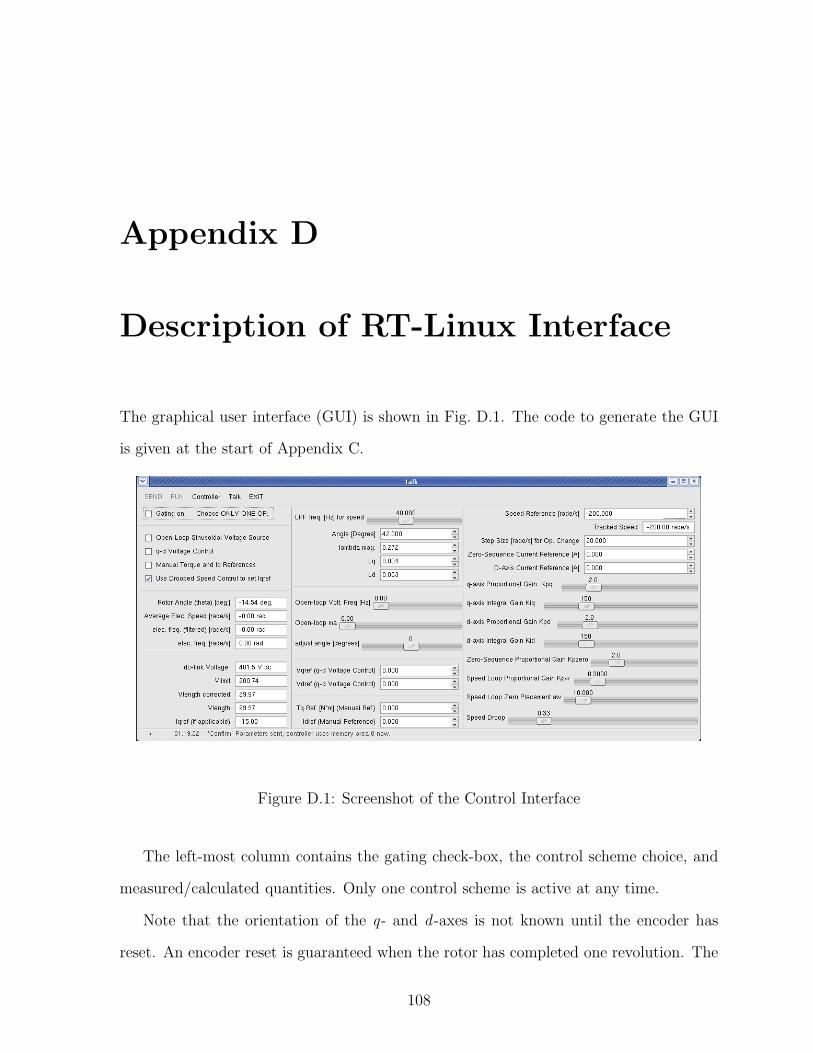
Appendix D
Description of RT-Linux Interface
The graphical user interface (GUI) is shown in Fig. D.1. The code to generate the GUI
is given at the start of Appendix C.
Figure D.1: Screenshot of the Control Interface
The left-most column contains the gating check-box, the control scheme choice, and
measured/calculated quantities. Only one control scheme is active at any time.
Note that the orientation of the q- and d -axes is not known until the encoder has
reset. An encoder reset is guaranteed when the rotor has completed one revolution. The
108
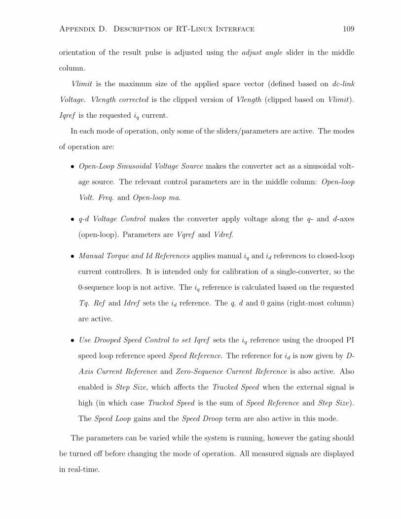
Appendix D. Description of RT-Linux Interface 109
orientation of the result pulse is adjusted using the adjust angle slider in the middle
column.
Vlimit is the maximum size of the applied space vector (defined based on dc-link
Voltage. Vlength corrected is the clipped version of Vlength (clipped based on Vlimit).
Iqref is the requested iq current.
In each mode of operation, only some of the sliders/parameters are active. The modes
of operation are:
• Open-Loop Sinusoidal Voltage Source makes the converter act as a sinusoidal volt-
age source. The relevant control parameters are in the middle column: Open-loop
Volt. Freq. and Open-loop ma.
• q-d Voltage Control makes the converter apply voltage along the q- and d -axes
(open-loop). Parameters are Vqref and Vdref.
• Manual Torque and Id References applies manual iq and id references to closed-loop
current controllers. It is intended only for calibration of a single-converter, so the
0-sequence loop is not active. The iq reference is calculated based on the requested
Tq. Ref and Idref sets the id reference. The q, d and 0 gains (right-most column)
are active.
• Use Drooped Speed Control to set Iqref sets the iq reference using the drooped PI
speed loop reference speed Speed Reference. The reference for id is now given by D-
Axis Current Reference and Zero-Sequence Current Reference is also active. Also
enabled is Step Size, which affects the Tracked Speed when the external signal is
high (in which case Tracked Speed is the sum of Speed Reference and Step Size).
The Speed Loop gains and the Speed Droop term are also active in this mode.
The parameters can be varied while the system is running, however the gating should
be turned off before changing the mode of operation. All measured signals are displayed
in real-time.

Appendix D. Description of RT-Linux Interface 110
The LPF freq [Hz] for speed is used to filter the feedback speed used for cancellation
of the cross-coupling terms and for input to the speed control loop.