in this project blocks used logic circuits no.35...
TRANSCRIPT

84 Otona no Kagaku
Circuit SchematicBlock Layout Diagram * In blocks with lighter lines, current only flows along the dark, solid lines.
Blocks used
in this project
No.35 Principles of a Basic AND Gate CircuitThis circuit is formed of lead blocks, an LED, and the two lead wires only. Insert the blocks and connect the lead wires as shown in the figure, and turn the main switch on.The LED will light up. If you disconnect either lead wire A or B, the LED will turn off. The LED will thus not turn on unless both lead wire terminals A and B are firmly inserted into the block connections as indicated.
Logic Circuits
● Circuit Logic
Computers can process and make a variety of judgments. However, computers do not act independently but merely analyze data to make detailed decisions that match the conditions set by a human operator. Looking at the patterns by which human beings make decisions, you can see that you can break them down into basic types. Logic circuits (also called logic gates) are used to express circuits that perform logical calculations broken down into the most basic patterns available (AND, OR, NOT, and other such simple logic expressions). All digital devices, no matter how simple or complex, contain a small computer used to process logic operations. This computer unit is formed of complex combinations of logic circuits, which allow it to process a wide variety of judgments.
What logic circuits are...
There are four different patterns of circuit operation that can be considered here. 1) Both lead terminals A and B are off (neither end of A or B is inserted into the blocks), 2) only lead terminal A is turned on (both ends of A are inserted into the block), 3) only lead terminal B is turned on, and 4) both lead terminals A and B are on. With this circuit, the LED will only turn on in case 4. This logic circuit is expressed as A AND B, or A • B. A value of "1" indicates that electricity is flowing, and a value of "0" indicates that electricity is not flowing. The truth table for an AND gate using this notation is given at right. Another way to express the relationships between inputs A and B and the output visually is to use a Venn diagram. Expressing this in a Venn diagram, the overlapping portion between variable A and variable B indicates A AND B (A • B).
• Logic gate symbol for an AND gate
• Venn diagram
0
0
0
1
A • B
0
1
0
1
A
0
0
1
1
B
1
2
3
4
Input Output

85E l e c t r o n i c B l o c k s m i n i C i r c u i t G u i d e
Circuit Schematic
Blocks used
in this project
Block Layout Diagram * In blocks with lighter lines, current only flows along the dark, solid lines.
No.36 Principles of a Basic OR Gate CircuitIn an AND gate circuit, the two lead wires are both connected in series, but in an OR gate circuit, they are connected in parallel. Insert the blocks and connect lead wires A and B as shown in the figure. Turn the main switch on. The LED will light up. The LED will turn on even if you disconnect either one of the two lead wires. The LED will only turn off if you disconnect both lead wires. The explanation given here is for a single, independent logic gate circuit with a simple structure. Logic gates can be connected together in more complicated configurations to produce a computer that operates in a way that closely resembles the way in which the human brain operates.
Logic Circuits
● Circuit LogicThere are four different patterns of circuit operation that can be considered here. 1) Both lead terminals A and B are off, 2) only lead terminal A is turned on, 3) only lead terminal B is turned on, and 4) both lead terminals A and B are on. With this circuit, the LED will only turn on in cases 2, 3 and 4, out of the four patterns given. This logic circuit is expressed as A OR B, or A + B. A value of "1" indicates that electricity is flowing, and a value of "0" indicates that electricity is not flowing. The truth table for an OR gate using this notation is given at right. Expressing this in a Venn diagram, the portions occupied by variable A or variable B or both indicates A OR B (A + B).
• Logic gate symbol for an OR gate
• Venn diagram
0
1
1
1
A + B
0
1
0
1
A
0
0
1
1
B
1
2
3
4
Input Output
One of the first research papers to be published that described the workings of what we view as the early modern computer was the famous First Draft of a Report on the EDVAC written by John von Neumman and published in 1945. This is why computer architecture is often referred to as Von Neumann architecture. Von Neumann architecture involves equipping computers with internal stored programs. These contributions to the development of the computer were quite considerable.Two men, Mauchly and Eckert, produced the first modern computer in the world, the ENIAC, in 1946. The ENIAC did not use the Von Neumann stored-program concept but rather a rewiring method.
Birth of the Computer (1)

86 Otona no Kagaku
Circuit SchematicBlock Layout Diagram * In blocks with lighter lines, current only flows along the dark, solid lines.
Blocks used
in this project
No.37 Principles of a Basic NOT Gate Circuit
Insert the blocks and connect the lead wires as shown in the figure, and turn the main switch on. The LED will light up. Touching the lead wire terminals together will cause the LED to turn off. Releasing the terminals will allow the LED to turn back on.
Logic Circuits
Recent vehicles are equipped with a warning buzzer that sounds if you open the driver-side door with the key in the ignition and the engine turned off. Let’s try to recreate this type of circuit using logic gates. Let the output be “1” for each of the following conditions: the key is in the ignition, the engine is on, the door is open, and the buzzer sounds. Let the opposite state for each condition, for example, when the key is taken out, be “0.” The buzzer is to sound when the key is “1,” the engine is “0,” and the door is “1.” In this case, the engine input should be connected to the buzzer output through a NOT gate and that for the key and door through an AND gate. The logic gate symbol for this relationship is shown in the figure at right.
Practical example of using this logic gate: "Key-in-ignition" warning alarm circuit
1
0
1
2
Input Output
A
0
1
A
EngineKey
DoorBuzzer
● Circuit LogicThis type of circuit is used where it is desired to obtain results opposite those of the command given. This logic circuit is expressed as NOT A, or Ā. A value of "1" indicates that the switch is turned on, and a value of "0" indicates that the switch is turned off. The truth table for a NOT gate using this notation is given at right. Expressing this in a Venn diagram, portions outside of A represent NOT A (Ā).
• Logic gate symbol for a NOT gate
• Venn diagram
* Make sure to touch something metal before starting this experiment (like a metal doorknob or window frame) in order to discharge any static electricity you may have built up in your body. When holding onto the lead wire terminals, make sure to grip the black wire coverings.

87E l e c t r o n i c B l o c k s m i n i C i r c u i t G u i d e
Circuit Schematic
Blocks used
in this project
Block Layout Diagram * In blocks with lighter lines, current only flows along the dark, solid lines.
No.38 Principles of a Basic NAND Gate Circuit
Insert the blocks as shown in the figure and turn the main switch on without connecting the lead wires. The LED will light up. Next, turn either lead wire A or B on (insert both ends of A or both ends of B as shown). The LED should remain unchanged (and stay on). If you turn both lead wires on, the LED will turn off.
Logic Circuits
ENIAC, the first general-purpose computer in the world was first displayed to the public in 1946. It used 18,000 vacuum tubes, 70,000 resistors, 10,000 capacitors, and 6,000 switches. It also weighed 30 tons and was 3 m in height. Part of this computer can still be seen on display in the museum for its historical value.The transistor was invented the following year, in 1947, by three men working at Bell Labs, including William Shockley. The transistor was small and light-weight, did not use much electricity, and had a long life. It helped advance further development of the computer. The following year, 1948, also marked important advancements in the field of computers. It was the year during which Claude Shannon published his famous thesis on information theory and Boolean logic. This helped to further pave the way for digital computing. The basic principles behind the modern computer were thus created and finalized in the span of3 or 4 years.
Birth of the Computer (2)
● Circuit LogicThe NAND logic gate combines together the NOT logic gate and the AND logic gate. This logic circuit is expressed as A NAND B, or A • B. A value of "1" indicates that the switch is turned, and a value of "0" indicates that the switch is turned off. The truth table for a NAND gate using this notation is given at right. Expressing this in a Venn diagram, the portions not included in the overlapping portion between variable A and variable B indicate A NAND B ( A • B ).
1
1
1
0
0
1
0
1
A
0
0
1
1
B
1
2
3
4
Input Output
A • B
• Logic gate symbol for a NAND gate
• Venn diagram

88 Otona no Kagaku
Circuit SchematicBlock Layout Diagram * In blocks with lighter lines, current only flows along the dark, solid lines.
Blocks used
in this project
No.39 Principles of a Basic NOR Gate Circuit
Insert the blocks as shown in the figure and turn the main switch on without connecting the lead wires. At this point, the LED will turn on. Next, turn either lead wire A or B on (insert both ends of A or both ends of B as shown). The LED should turn off. The LED will also turn off if you turn both A and B on.
Logic Circuits
The famous genius mathematician George Boole was the first to write about his logic theory involving AND, OR, NOT, NOR, and NAND operations. He published his first major work on the subject in 1847. The theories he proposed in his thesis are referred to as “logical algebra” or “Boolean algebra” and are used to express logical constructs in terms of mathematical concepts. In 1948, Claude Shannon published a thesis that stated that all information could be conveyed using Boolean algebra. Shannon’s ideas advanced the development of digital circuits. They form the basis upon which all modern digital circuits and computers are constructed. Claude Shannon, considered the father of information communication theory, passed away in 2001 at the age of 84, leaving behind quite a number of remarkable contributions to the fields of mathematics and technology. We owe a great deal to these two men, Boole and Shannon, for their contributions. If either of these men had not existed, the fields of digital technology and computers may never have come into being.
George Boole and Claude Shannon
1
0
0
0
0
1
0
1
A
0
0
1
1
B
1
2
3
4
Input Output
A + B
● Circuit LogicThis logic gate circuit uses a combination of the OR logic gate and the NOT logic gate. This logic circuit is expressed as A NOR B, or A+B . A value of "1" indicates that the switch is turned on, and a value of "0" indicates that the switch is turned off. The truth table for a NAND gate using this notation is given at right. Expressing this in a Venn diagram, only the portions not occupied by either variable A or variable B or the overlap of A and B are included in A NOR B ( A+B ).
• Logic gate symbol for a NOR gate
• Venn diagram

89E l e c t r o n i c B l o c k s m i n i C i r c u i t G u i d e
Circuit Schematic
Blocks used
in this project
Block Layout Diagram * In blocks with lighter lines, current only flows along the dark, solid lines.
The sound produced with the earphone-based lie detector in Circuit No. 24 is output by a speaker from an IC amplifier. If you connect the terminal closest to the plus (+) terminal on the earphone in the earphone-based circuit to the IN terminal, you can connect the earphone to the IC amplifier in the circuit board. It is recommended that you connect a 10-kΩ to 80-kΩ resistor (here, a 20-kΩ resistor is used) between the terminals to prevent clipping (a type of distortion) in the sound.
No.40 Lie Detector (Speaker-based)Insert the blocks as shown in the figure and then turn on the main switch. Have a person hold the lead wires, one in each hand, which should produce a sound from the speaker. At this time, the person holding onto the lead wires is applying an added resistance to the circuit. If the person tells a lie, the amount of resistance they apply will change, which will change the pitch or volume of the sound produced, even if only slightly (see Circuit No. 24 for details on how to use a lie detector). Sound is produced using the blocking oscillator oscillating method. Note: As this is merely a type of experiment examining the operation of an electric circuit, it cannot be determined with absolute certainty whether or not the person under test is actually telling a lie.
Fun Circuits
Have the person you intend to test lightly grasp onto the lead wire terminals and then turn the tuning knob all the way to the right (if the sound produced is too loud, adjust the volume). Turn the tuning knob slowly to the left until the sound becomes somewhat stabilized then release your hand from the knob. This completes the adjustments for the test.
• Making adjustments before starting the experiment
* The volume may be too low in some cases depending on the person under test. If this is the case when you attempt this experiment, try changing out the 0.05-μF capacitor and replacing it with the 0.1-μF capacitor, making sure to orient the block in the proper direction. A different capacitance should provide you with a greater range to change the volume from when you first start hearing sound come out.
● Circuit Mechanism
* Make sure to touch something metal before starting this experiment (like a metal doorknob or window frame) in order to discharge any static electricity you may have built up in your body. When holding onto the lead wire terminals, make sure to grip the black wire coverings.

90 Otona no Kagaku
Circuit SchematicBlock Layout Diagram * In blocks with lighter lines, current only flows along the dark, solid lines.
Blocks used
in this project
No.41 Electronic Sleep Sound MachineInsert the blocks and connect the earphone as shown in the figure and then turn the main switch on. A steady, rhythmic series of ticking sounds should be emitted from the earphone at set intervals.You may not be able to hear the sounds if you turn the tuning knob too far to the right or left. Experiment with the knob to find the setting that produces the best sound output, which should be somewhere in the middle. One of the characteristics of this circuit is that it generates blocking oscillation using a transistor and an antenna coil (tuning coil).
Fun Circuits
Try replacing the 10-μF capacitor in the block layout diagram with the 47-μF capacitor block, making sure to orient the block in the proper direction. Changing the capacitor block should increase the length of the interval between sounds produced by the oscillator by around 5 times (to around 20 seconds). Try it out to see what happens.Caution: Make sure to turn the main switch off before changing out any blocks.
• Try changing out the capacitor block
This circuit is formed of a transistor, capacitor, and antenna coil configuration that can be used to generate blocking oscillation. Normally, this type of circuit would use a transformer to produce the necessary induction effect but here we will instead use an antenna coil. With an antenna coil, however, the induction effect is rather weak as there is no magnetic core involved to magnify the effect. The antenna coil should adequately fulfill our requirements as we do not need or want the intense blocking oscillation effect a transformer would produce.The antenna coil we use here is a high-frequency coil. The question is, then, why the sounds we produce end up being low in frequency if we are using a high-frequency coil. Current flows into the base on the transistor drawn by the low-resistance 1-kΩ resistor. This causes a large amount of current approaching the maximum allowable value to flow into the collector. The blocking oscillation produced by the charging of the 10-μF capacitor is even more prominent than the high-frequency oscillation generated by the antenna coil and capacitor. In most cases, blocking oscillation is a low-frequency oscillation effect. This circuit also uses a 10-μF capacitor, which has a rather high capacitance. This capacitor begins charging when the main switch is turned on and current begins to flow through the base. A large amount of current flows through the base at this time. Conversely, the current flowing in the opposite direction that is induced by the coil is relatively weak, which allows the capacitor to continue charging without being adversely affected by this reverse current. Once the capacitor has finished charging, it beings discharging through the 1-MΩ and 1-kΩ resistors, which is when blocking oscillation occurs.
To generate blocking oscillation with the antenna coil...
91E l e c t r o n i c B l o c k s m i n i C i r c u i t G u i d e
Circuit Schematic
Blocks used
in this project
Block Layout Diagram * In blocks with lighter lines, current only flows along the dark, solid lines.
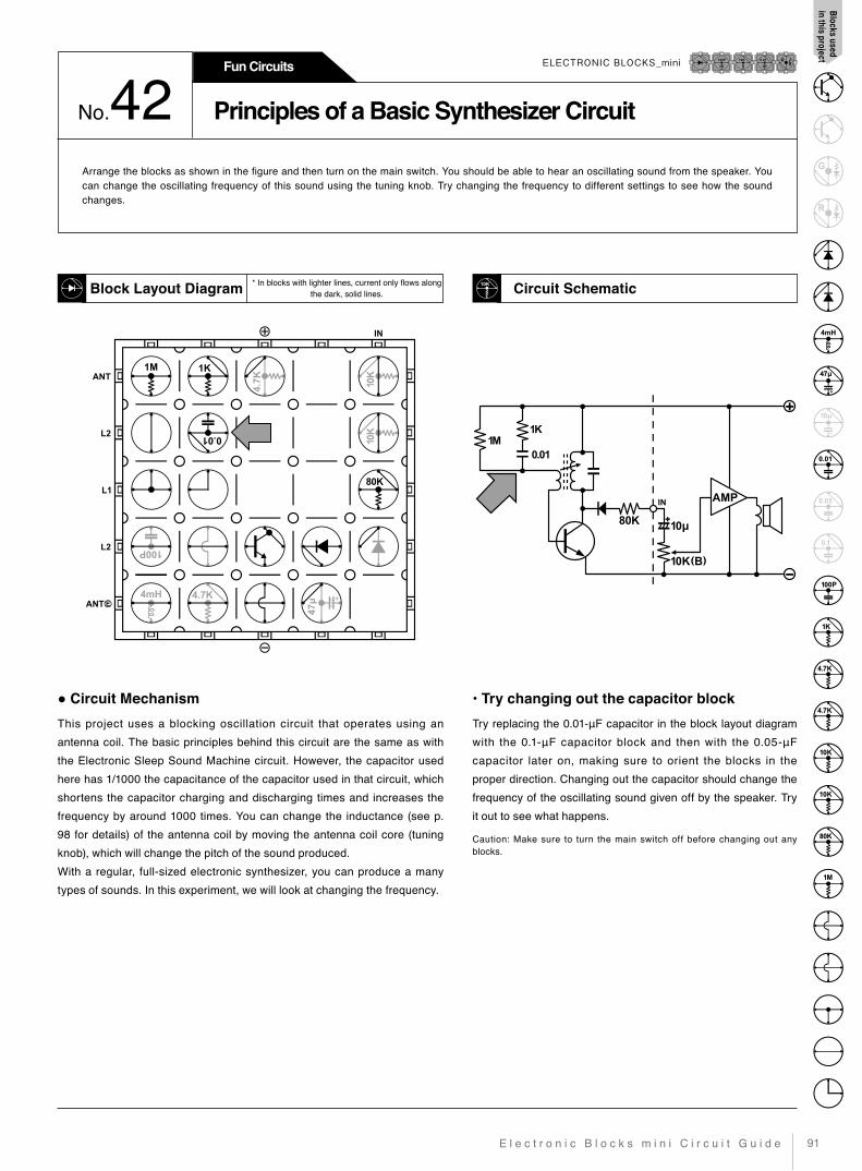
No.42 Principles of a Basic Synthesizer Circuit
Arrange the blocks as shown in the figure and then turn on the main switch. You should be able to hear an oscillating sound from the speaker. You can change the oscillating frequency of this sound using the tuning knob. Try changing the frequency to different settings to see how the sound changes.
Fun Circuits
Try replacing the 0.01-μF capacitor in the block layout diagram with the 0.1-μF capacitor block and then with the 0.05-μF capacitor later on, making sure to orient the blocks in the proper direction. Changing out the capacitor should change the frequency of the oscillating sound given off by the speaker. Try it out to see what happens.
Caution: Make sure to turn the main switch off before changing out any blocks.
• Try changing out the capacitor blockThis project uses a blocking oscillation circuit that operates using an antenna coil. The basic principles behind this circuit are the same as with the Electronic Sleep Sound Machine circuit. However, the capacitor used here has 1/1000 the capacitance of the capacitor used in that circuit, which shortens the capacitor charging and discharging times and increases the frequency by around 1000 times. You can change the inductance (see p. 98 for details) of the antenna coil by moving the antenna coil core (tuning knob), which will change the pitch of the sound produced.With a regular, full-sized electronic synthesizer, you can produce a many types of sounds. In this experiment, we will look at changing the frequency.
● Circuit Mechanism
92 Otona no Kagaku
Circuit SchematicBlock Layout Diagram * In blocks with lighter lines, current only flows along the dark, solid lines.
Blocks used
in this project
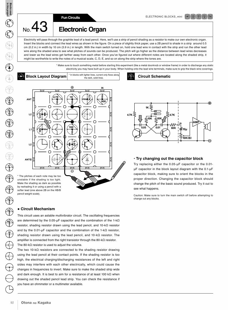
No.43 Electronic OrganElectricity will pass through the graphite lead of a lead pencil. Here, we'll use a strip of pencil shading as a resistor to make our own electronic organ. Insert the blocks and connect the lead wires as shown in the figure. On a piece of slightly thick paper, use a 2B pencil to shade in a strip around 0.5 cm (0.2 in.) in width by 10 cm (3.9 in.) in length. With the main switch turned on, hold one lead wire in contact with the strip and run the other lead wire along the shaded area to see what pitches of sounds can be produced. The pitch will go higher as the distance between lead wires decreases and lower as the lead wires get farther away from each other. Once you’ve figured out where different notes are located along the shaded strip, it might be worthwhile to write the notes of a musical scale, C, D, E, and so on along the strip where the tones are.
Fun Circuits
Try replacing either the 0.05-μF capacitor or the 0.01-μF capacitor in the block layout diagram with the 0.1-μF capacitor block, making sure to orient the blocks in the proper direction. Changing the capacitor block should change the pitch of the basic sound produced. Try it out to see what happens.
Caution: Make sure to turn the main switch off before attempting to change out any blocks.
• Try changing out the capacitor block
* The pitches of each note may be too unstable if the shading is too light. Make the shading as dark as possible by reshading it or using a pencil with a softer lead (one above 2B on the HB/B pencil weight scale).
This circuit uses an astable multivibrator circuit. The oscillating frequencies are determined by the 0.05-μF capacitor and the combination of the 1-kΩ resistor, shading resistor drawn using the lead pencil, and 10-kΩ resistor and by the 0.01-μF capacitor and the combination of the 1-kΩ resistor, shading resistor drawn using the lead pencil, and 10-kΩ resistor. The amplifier is connected from the right transistor through the 80-kΩ resistor.The 80-kΩ resistor is used to adjust the volume.The two 10-kΩ resistors are connected to the shading resistor drawing using the lead pencil at their contact points. If the shading resistor is too high, the electrical charging/discharging resistances of the left and right sides may interfere with each other electrically, which could cause the changes in frequencies to invert. Make sure to make the shaded strip wide and dark enough. It is best to aim for a resistance of at least 100 kΩ when drawing out the shaded pencil lead strip. You can check the resistance if you have an ohmmeter or a multimeter available.
● Circuit Mechanism
* Make sure to touch something metal before starting this experiment (like a metal doorknob or window frame) in order to discharge any static electricity you may have built up in your body. When holding onto the lead wire terminals, make sure to grip the black wire coverings.

93E l e c t r o n i c B l o c k s m i n i C i r c u i t G u i d e
Circuit Schematic
Blocks used
in this project
Block Layout Diagram * In blocks with lighter lines, current only flows along the dark, solid lines.
No.44 Light-based Morse Code Practice Circuit
Although this is a rather simple circuit, it can be used for practicing Morse code. This circuit produces Morse code signals not with sound but with light. Insert the blocks and connect the lead wires as shown in the figure, and turn the main switch on. Touch the lead wire terminals together to turn the LED on.
Fun Circuits
You can make the LED flash briefly to create a “dot” (short pulse) signal by touching the lead wire terminals together and releasing them quickly.
* Make sure to touch something metal before starting this experiment (like a metal doorknob or window frame) in order to discharge any static electricity you may have built up in your body. When holding onto the lead wire terminals, make sure to grip the black wire coverings.

94 Otona no Kagaku
Circuit SchematicBlock Layout Diagram * In blocks with lighter lines, current only flows along the dark, solid lines.
Blocks used
in this project
No.45 Darlington Love TesterInsert the blocks and connect the lead wires as shown in the figure. Have two people hold onto the lead wire terminals, each person holding onto one. Turn the main switch on. Have the two people press the pointer fingers on their free hands together as shown in the photograph below. If the two people are compatible with each other, the LED will turn on. The LED may also turn on if they touch some other object at the same time. The LED will turn on if the other object is a conductor (see Circuit No. 07 for details) with low resistance. The two transistors in this circuit are connected together using a "Darlington connection." Note: The exercise described above for this circuit project is merely an experiment. This circuit test cannot be used to determine with absolute accuracy whether two people are compatible with each other or not.
Fun Circuits
The LED will turn on if the two people touch their pointer fingers together with their free hands while holding onto one of the terminals in.
The collectors on the two transistors in this circuit are connected together in parallel. The emitter on the first transistor is connected to the base of the second transistor, and the two transistors connected thus are treated as a single transistor. This type of transistor connection is called a “Darlington connection,” also known as a “Darlington pair.” The main feature of the Darlington connection is that you can use it to control an extremely large collector current using a very small base current. The electrical resistance of the human body is extremely high, which allows the human body to pass relatively slight amounts of current. This connection method works well in turning on an LED at a high brightness using these slight changes in current.
What is a Darlington transistor connection?
First transistor
Collector currentBase
currentSecond
transistor
* Make sure to touch something metal before starting this experiment (like a metal doorknob or window frame) in order to discharge any static electricity you may have built up in your body. When holding onto the lead wire terminals, make sure to grip the black wire coverings.

95E l e c t r o n i c B l o c k s m i n i C i r c u i t G u i d e
Circuit Schematic
Blocks used
in this project
Block Layout Diagram * In blocks with lighter lines, current only flows along the dark, solid lines.
No.46 Reflex Tester
Insert the blocks and connect the lead wires as shown in the figure, and turn the main switch on. In quick succession, repeatedly touch the lead wires together and pull them apart to turn the LED on. If you move too slowly, the LED will turn on and off intermittently in a clear pattern, and the faster you go, the more it will look as if the LED is staying on constantly, which makes this exercise a good test of your reflexes.
Fun Circuits
Touch the lead wire terminals together and release them q u i c k l y i n r a p i d , repeated succession to get the LED to flash on and off at rapid speed.
When you touch the lead wire terminals together, current will flow through the 10-μF capacitor for a short time, which will turn the left transistor on momentarily and cause the charge stored in the 47-μF capacitor to discharge instantaneously. Having discharged all of the charge it had stored up, the 47-μF capacitor will begin charging again, causing the LED to turn on. The LED will turn off once again when charging is finished. The charge stored in the 10-μF capacitor is released through the 4.7-kΩ resistor.
● Circuit Mechanism
Why does the LED look like it is on all the time when the lead wire terminals are touched together and released at rapid speed?To find the answer to this question, first, take a look at the figure on the left below. The current flowing through the LED is plotted along the vertical axis (y-axis) and time along the horizontal axis (x-axis). The length of time during which the LED will stay on is determined at least in part by the capacity of the capacitors used. Capacitors with higher capacitances can store greater amounts of charge, which will lengthen the amount of time that a transistor can remain on during charging, discharging, and regular operation. The amount of time that it takes any individual to touch the lead wire terminals together and release them will also vary by person. As the length of the interval between when the terminals are touched together becomes shorter, the length of time that the LED stays off will also get shorter. This will cause the LED to look like it is turned on continuously.
Reasons why the LED looks to be fully and continuously lit up
LED on
Switch on Switch on
Switch off Switch off
LED on Time Time
Current flow
ing to the LED
Current flow
ing to the LED
* Make sure to touch something metal before starting this experiment (like a metal doorknob or window frame) in order to discharge any static electricity you may have built up in your body. When holding onto the lead wire terminals, make sure to grip the black wire coverings.

96 Otona no Kagaku
Circuit SchematicBlock Layout Diagram * In blocks with lighter lines, current only flows along the dark, solid lines.
Blocks used
in this project
No.47 Light-based Circuit Disconnect AlarmThis is the same type of circuit device as in Circuit No. 23, only using light instead of sound. Insert the blocks and connect the lead wires as shown in the figure. Connect the lead wire terminals together using a paper clip as shown in the photograph. Turn on the main switch. The green LED should light up brightly and the red LED somewhat faintly. If you disconnect either lead wire terminal from the paper clip, the green LED will turn off, and the red LED will begin to light up brightly.
Fun Circuits
While the lead wire terminals are in contact with each other, the electric potential of the base on the left transistor drops, causing the transistor to turn off and the electric potential of the collector to remain stable at a high level. When current flows through the red LED and 80-kΩ resistor into the base on the right transistor, the right transistor turns on, and the green LED lights up. This base current will also cause the red LED to light up faintly. When the lead wires are disconnected from each other, current flows through the base on the left transistor through the 10-kΩ resistor, causing the red LED to light up brightly. The electric potential at the base of the right transistor then drops, causing the green LED to turn off.
● Circuit Mechanism
How to connect the lead wires together using a paper clip
The resistor blocks (the one 1-kΩ, two 4.7-kΩ, two 10-kΩ, one 80-kΩ, and one 1-MΩ resistor blocks) can be connected together in series or in parallel to produce an even greater range of available resistance values. Formulas for calculating resistance values for combinations of resistors connected in series and parallel are given below. * Rp represents the resultant resistance for each of the two combinations as shown.
Creating other resistor combinations using the limited number of resistor blocks
Connected in parallel
Example: 1K+4.7K=5.7K 10K+4.7K=14.7K 10K+10K=20K 80K+1M(1000K)=1080K
Example: (1K×4.7K)/(1K+4.7K)=0.82K (10K×4.7K)/(10K+4.7K)=3.2K (1000K×80K)/(1000K+80K)=74K
Connected in series

97E l e c t r o n i c B l o c k s m i n i C i r c u i t G u i d e
Circuit Schematic
Blocks used
in this project
Block Layout Diagram * In blocks with lighter lines, current only flows along the dark, solid lines.
No.48 Principles of a Basic Automotive Turning Signal Circuit
Automatic LED flasher circuits are used in a wide variety of applications including pedestrian signal lights and automotive turning signals. Insert the blocks and connect the lead wires as shown in the figure, and turn the main switch on. Touch the lead wire terminals together to cause the LED to flash on and off. Release the lead wire terminals to turn the LED completely off.
Fun Circuits
This circuit uses an astable multivibrator circuit. The 4.7-kΩ resistor, 10-kΩ resistor, and 47-μF capacitor set the length of time that the LED stays lit up, and the 10-kΩ resistor and 10-μF capacitor set the length of time that the LED stays off. It takes around 0.5 seconds for the circuit to complete one cycle. If you replace the 10-kΩ resistor connected to the 10-μF capacitor (the resistor indicated by the arrow in the figure) with the 80-kΩ resistor, you can lengthen the length of time that the LED stays off and lengthen the cycle time from 0.5 seconds to around 1 second. Oscillation is turned on and off according to the on/off state of the power supply (earth ground side), which in turn, is based on the lead wire terminals being touched together and separated.
● Circuit Mechanism
The capacitor blocks (one each of 100 pF, 0.01 μF, 0.05 μF, 0.1 μF, 10 μF, and 47 μF) can be connected together in series or in parallel to produce an even greater range of available capacitance values. Formulas for calculating capacitance values for combinations of capacitors connected in series and parallel are given below.* Cp represents the resultant capacitance for each of the two combinations as shown.
Creating other capacitor combinations using the limited number of capacitor blocks
Connected in parallel
0.01µF+0.05µF=0.06µF0.05µF+0.1µF=0.15µF10µF+47µF=57µF
* When capacitors are connected together in parallel, the total resultant capacitance is higher than with series connections because the total amount of charge that can be stored increases as compared to that for each individual capacitor.
Connected in series
(0.01µF×0.05µF)/(0.01µF+0.05µF)=0.0083µF(0.1µF×0.05µF)/(0.1µF+0.05µF)=0.033µF(10µF×47µF)/(10µF+47µF)=8.2µF
* Capacitors are formed of an insulator sandwiched between two electrodes.When capacitors are connected together in series, the total resultant capacitance calculated using the contributions from each individual capacitor is lower than the sum of the individual capacitances because the distance between the two electrode plates increases.
Example:)
Example:
* Make sure to touch something metal before starting this experiment (like a metal doorknob or window frame) in order to discharge any static electricity you may have built up in your body. When holding onto the lead wire terminals, make sure to grip the black wire coverings.

98 Otona no Kagaku
Circuit SchematicBlock Layout Diagram * In blocks with lighter lines, current only flows along the dark, solid lines.
Blocks used
in this project
No.49 Principles of a Basic Railway Crossing Alarm Circuit
Let’s put together a fun and interesting circuit that is made using two LEDs. Arrange the blocks as shown in the figure and then turn on the main switch. The two LEDs will turn on and off in alternating fashion. This particular circuit is a type of astable multivibrator circuit. It is used in alarm devices at railway crossings to warn of oncoming trains along with other similar applications.
Fun Circuits
This circuit uses an astable multivibrator circuit. The 4.7-kΩ resistor, 80-kΩ resistor, and 10-μF capacitor set the length of time that the red LED stays lit up, and the 10-kΩ resistor and 47-μF capacitor set the length of time that the green LED stays lit up. It takes around 0.5 seconds for the circuit to complete one cycle. The right transistor is connected to the amplifier circuit through the 0.1-μF capacitor. A short, staccato popping sound is amplified and emitted by the speaker in rhythm with the illumination of the LEDs.
● Circuit Mechanism
Capacitors and electromagnetic coils differ from resistors in that the phase of the current flowing through them changes in response to changes in voltage. For this reason, the resistance of capacitors and coils in AC circuits is expressed not in terms of regular resistance but in terms of a property called electrical impedance. More specifically, the impedance of a capacitor is called its capacitance and that of a coil its inductance. The impedance of a resistor is its resistance. Therefore, the sum of impedances in circuit can be thought of in terms of the resistance, capacitance, and inductance of the electrical components in the circuit as written below.
What is impedance?
Capacitance and inductance values will change in response changes in the AC frequency. For this reason, they are usually written with respect to a standard frequency (there are actually many different methods for expressing the capacitances and inductances of related components, but we will use the method given here).
Example: Consider an earphone that is imprinted with an impedance label of “32 Ω (1 kHz).” This notation indicates a resistance of 32 Ω when the earphone is emitting beeping sounds at a frequency of 1 kHz.
Impedance = Resistance + Capacitance + Inductance(Resistors) (Capacitors) (Electromagnetic coils)

99E l e c t r o n i c B l o c k s m i n i C i r c u i t G u i d e
Circuit Schematic
Blocks used
in this project
Block Layout Diagram * In blocks with lighter lines, current only flows along the dark, solid lines.
No.50 Electronic FireflyYears ago, the firefly was one of the nighttime symbols of summer, seen and loved by many. Here, we will try to recreate the captivating flickering light of a firefly using the Electronic Blocks mini supplement. Arrange the blocks as shown in the figure and then turn on the main switch. The green LED will turn on and then start flashing after a certain amount of time passes. This circuit attempts to recreate the look of a firefly’s light using an astable multivibrator circuit. The circuit cycles through a pattern in which the left and right LEDs flash on and off repeatedly. The timing of the flash pattern is adjusted using the electrolytic capacitors connected to the bases of the transistors.
Fun Circuits
This circuit uses an astable multivibrator circuit. The 1-MΩ resistor and 10-μF capacitor set the length of time that the LED stays lit up, and the 80-kΩ resistor, 4.7-kΩ resistor, and 47-μF capacitor set the length of time that the LED stays off. It takes around 7 seconds for the circuit to complete one cycle. Replacing the 4.7-kΩ resistor connected in series to the 47-μF capacitor with a resistor with a higher resistance will shorten the length of time that the LED is turned off. The collector resistor on the left transistor (the 1-kΩ resistor connected to the collector on the left transistor) is a load resistor.
● Circuit Mechanism