in-house rapid pcb prototyping product catalog
TRANSCRIPT

In-House Rapid PCB Prototyping Product Catalog
Circuit Board Plotters
Laser Structuring
Through-Hole Plating
Multilayers
SMT/Finishing
Micro Material Processing
Visit our
Virtual Showroom:
PCB Prototyping
Equipment in a
360-degree View

Do you have any Questions about your Order? Do you Require Technical Service?
You can find all sales and service contact information below.
Our experienced employees will be happy to assist you.
LPKF AG has a global sales network. An overview of all LPKF representatives can be found on page 57.
For more information, please visit our website at www.lpkf.com.
Germany (LPKF Headquarters)Phone +49 (5131) 7095-0Fax +49 (5131) 7095-90
E-Mail [email protected] [email protected]
Website www.lpkf.com
North/Central AmericaPhone +1 (503) 454-4200Fax +1 (503) 682-7151
E-Mail [email protected] [email protected]
Website www.lpkfusa.com
ChinaPhone Sales +86 (22) 2378-5318 Service +86 (22) 2378-5328
E-Mail [email protected] Website www.lpkf.cn
JapanPhone +81 47 432-5100Fax +81 47 432-5104
E-Mail [email protected] Website www.lpkf.jp
South KoreaPhone +82 (31) 689 3660Fax +82 (31) 478 5988
E-Mail [email protected] Website www.lpkf.kr
LPKF Sales and Service
Worldwide LPKF Representatives
www.lpkf.com/distributor

1
Welcome to LPKF Rapid PCB Prototyping 2
PCB Prototyping Equipment in a 360-degree View 4
Rapid PCB Prototyping – The Faster Way to Create Circuit Boards 5
LPKF Circuit Board Plotters 6Overview of Application Areas 8LPKF ProtoMat E44 – Compact, Easy to Use, Precise 10LPKF ProtoMat S64 – An All-rounder for Rapid PCB Prototyping 11LPKF ProtoMat S104 – Specialist for RF and Microwave Applications 12Comparison of LPKF Circuit Board Plotters 13
Innovative Laser Technology for Rapid PCB Prototyping 14Laser Micro Material Processing 15LPKF ProtoLaser ST – Tabletop System for Laser Structuring of PCBs 17LPKF ProtoLaser S4 – Laser Processing of PCBs 18LPKF ProtoLaser U4 – Multipurpose Tool for the Electronics Lab 19LPKF ProtoLaser R4 – Specialist for Material-friendly Processing 20
LPKF CircuitPro – Smart Software with Intuitive Operation 21
Accessories for LPKF Circuit Board Plotters and ProtoLasers 25
Operating Materials for LPKF Circuit Board Plotters and ProtoLasers 28
LPKF Drilling and Milling Tools for LPKF ProtoMats 31
Systems and Processes for Manufacturing Component Population 33LPKF EasyContac – Manual Through-Hole Plating of Double-Sided PCBs 34LPKF ProConduct – Reliable Through-Hole Plating for PCB Prototyping with Conductive Paste 34LPKF Contac S4 – Table-Top Through-Hole Electroplating 35LPKF MultiPress S – A Press for Multilayer Production 36LPKF ProMask and ProLegend – Solder Masks and Legend Printing 37LPKF ProtoPrint S4 – SMT Stencil Printer for PCB Prototypes 38LPKF ProtoPlace E4 – Fast and Easy Positioning 39LPKF ProtoPlace S4 – SMD Pick & Place Machine for PCB Prototypes and Low Volumes 40LPKF ProtoFlow S4 – Reflow Oven for Lead-Free Soldering in the Lab 42Accessories for SMT Systems and Processes 43
Scientific Prototyping – Laser Systems for Development and Science 46Laboratory Laser Systems for Demanding Applications 48
Micro Material Processing Specialist 52
LPKF Service & Support – Secure Your Investment 55
LPKF International Contacts 57
Notes 59
Legal Information 60
Table of Contents

2
In this catalog, you will find everything you need for rapid prototyping of printed circuit boards:
machines, tools, consumables, accessories, and software. With this, you can manufacture single-
sided, double-sided, or even multilayer PCBs in-house.
Welcome to LPKF Rapid PCB Prototyping
Why Inhouse Prototyping? Because It’s Fast, Easy and Efficient.With increasing functionality, miniaturization and the demand for geometric precision, the requirements for prototyping are getting stricter. In line with the inno-vative power of the electronics industry, it makes sense to quickly turn developers’ ideas into functional models. With LPKF’s equipment, you can implement your PCBs directly and precisely, on-site in your own laboratory.
In PCB prototyping, there are many reasons for manufacturing assemblies quickly, cost-effectively and, if possible, without much additional effort:
• Sensitive data and circuits remain in the company’s own laboratory.
• Iteration steps can be created at short notice – no waiting for suppliers, no additional costs due to additional external (express) manufacturing.
• Developers with their own prototype production can influence the overall process.
• The time-to-market is reduced considerably accord-ing to the number of PCB samples – often a decisive competitive advantage.

3
Thin film double-sided structured with LPKF ProtoLaser R4 Double-sided FR4 material processed with LPKF ProtoMat S104
You want to use special or sensitive materials? Even special applications, which are often produced by service providers with considerable effort, can be produced effectively in the company’s own laboratory with LPKF in-house equipment.
An example: The LPKF ProtoLaser R4 paves the way for forward-looking innovations with the latest materials from research and development. The system is designed for special applications – such as research with thermally sensitive materials or with very robust materials – but the system can also process PCBs.
Picosecond-short laser pulses allow the structuring of sensitive substrates, as well as the cutting of hardened or fired technical substrates. The ProtoLaser R4 precision laser system thus opens up new microprocessing possibilities for experiments with completely new scientific materials in the company’s own laboratory.
Solutions for R & D Special Applications
The space required for in-house production equipment is less than commonly thought. In particular, chemical-free processes have a low space requirement because the expense is low compared to multi-stage bath sys-tems, which require the monitoring or disposal of the chemicals and have higher occupational health and safety requirements.
LPKF systems can be used to produce single- or double-sided PCBs, multilayers and rigid or flexible PCBs. In addition, the systems can create high-power circuits, as well as RF and microwave PCBs, allowing extremely exciting product options for electronics.
Thanks to our own sophisticated software, the operation of the systems is extremely simple. The user is guided through the individual process steps in such a way that PCB prototyping can be realized without extensive prior training.
And How Does the Production Process Work? Our LPKF TechGuide PCB Prototyping explains the individual process steps of PCB prototyping and helps with tips and tricks for the practical use of LPKF systems. Feel free to request the TechGuide or talk to our experts.
About LPKFWith decades of experience and many customized solutions, LPKF is the global market leader in rapid PCB prototyping, especially for PCBs. About 700 employees around the globe provide professional sales and service support.

4 https://product-showroom-dq.lpkf.com
PCB Prototyping Equipment in a 360-degree ViewFor development departments or institute laboratories that want to carry out their PCB prototyping
in-house, LPKF has the complete range of equipment in its portfolio: from circuit board plotters for
drilling and structuring to SMT stencil printers and reflow ovens to laser machines.
To give you a quick overview of the prototyping port-folio, we have set up a virtual showroom for you. It is also an informative alternative to visiting our booths or demo lab in times of travel restrictions.
You can visit the showroom simply via the link using your browser, which means you do not need any spe-cial software. Click through the exhibition and get to know the right systems for your laboratory and applica-tions the quick way. In addition to the range of products that has been tried and tested for years, four themati-cally structured rooms present systems that have only recently been launched on the market and our innova-tive software solutions:
• PCB Basic Line• Multilayer Production• RF Prototyping • Micro Material Processing
In the showroom display, the real sizes of the particularly compact LPKF laboratory systems can be clearly seen. Technical information on the individual systems is available, as are demo videos on the application areas – all in English. In this way, many questions about PCB prototyping can be quickly clarified. For any unanswered questions, as well as concrete application possibilities, you can reach our experts via a contact form.

5
Rapid PCB Prototyping – The Faster Way to Create Circuit BoardsSpeeding up development means getting to market more quickly. With the rapid PCB prototyping
solutions from LPKF, this is easy to accomplish. From mechanical or laser structuring of the base
material to production of the complex multilayer prototype. The entire prototyping cycle – from
design to production and optimization – can be run through in a single day using LPKF products.
PCB StructuringLPKF ProtoMats are setting global standards in precision, flexibility, and user-friendliness. LPKF circuit board plotters are indispensable for fast in-house production of PCBs – for quantities ranging from one-offs for development projects to small batches. They are ideal for high-capacity, analog, digital, RF, and microwave applications.
Made in Europe: for over four decades now, LPKF circuit board plotters have served as a benchmark in the milling, drilling, and contour milling of PCBs. Take for example LPKF ProtoMat S104: its high-capacity spindle and vacuum table it is also suitable for RF applications and thin laminates as well as substrates with a sensitive surface (PCBs up to 100 μm on FR4 18/18 Cu). The system software also takes into consideration special requirements of RF materials.
More demanding production methods can be handled with another LPKF product group: PCB structuring and micro material processing with LPKF’s ProtoLaser S4, ProtoLaser U4, and the compact table-top laser system LPKF ProtoLaser ST are setting new standards in quality, speed, and materials capabilities. You still don’t need to be afraid of our laser systems: thanks to our software, the operation is as simple as the operation of mechanical PCB plotters.
Multilayers, Through-Hole Plating, and AssemblyLPKF circuit board plotters are ideal for rapid proto-typing of multilayer PCBs. Combined with a multilayer press such as the LPKF MultiPress and a through-hole plating system, they can create high-grade multilayer PCBs for subsequent assembly with the
LPKF ProtoPlace. The advantages are especially evident in the development phase for complex designs.
Versatile SoftwareEach LPKF structuring system is delivered with a comprehensive software package that has been optimized for ease of use, maximum quality, and rapid generation of results. LPKF CircuitPro supports all standard CAD data file formats for import and transmits the production data to the structuring system.
Other ApplicationsAlong with being able to produce PCBs in record time, LPKF systems have proven their versatility in a wide variety of applications: from housings, front panels, aluminum and plastics processing, depaneling of assembled boards, and cutting and engraving of plastic films to geometrically precise structuring of ceramic RF boards.

6
LPKF Circuit Board Plotters
In-House Production of PCB Prototypes and Small BatchesLPKF’s ProtoMat systems are available in three different series. The ProtoMat E44 supplies LPKF quality at an entry-level price – without extra options and automation, but still offers the highest quality basic functionality.
The ProtoMat S systems are largely automated. They feature automatic tool changing, and can be used for other applications through a vacuum table and a
vision system. The systems feature a stable granite machine base and an attractive protection housing. The highly flexible system software LPKF CircuitPro allows for intuitive operation. A parameter library for various materials supports the user-friendliness. If necessary, the inte grated Process Guide leads the user step by step through the process.
Compact for any task: all ProtoMat systems only need one software-controlled user-optimized LPKF vaccum extraction system, power source, and compressed air.
Fast, precise, and easy – LPKF’s circuit board plotters have been meeting these user demands
for four decades.

7
High-Quality Equipment for New ApplicationsEven the simplest system, the ProtoMat E44, can mill, drill and route single- and double-sided PCBs with high quality.
The key features of all LPKF ProtoMats include:
Circuit board plotter spindles: The LPKF ProtoMats come with different milling spindles that rotate at speeds of 40 000 RPM to 100 000 RPM (controlled). A high spindle speed enables the selection of finer tools, faster processing, increases resolution, and improves side wall quality. Tool change: The ProtoMat E44 has collet chucks for manual tool changing, whereas the other ProtoMats independently select the tools. This allows for highly automated, unsupervised operation and slashes processing times. Another feature of the automatic
tool changer is the integrated automatic milling depth adjustment device.
Camera system: With the integrated registration camera system, the LPKF ProtoMat E44 achieves a precision of ± 20 μm for processing of double-sided PCBs with fiducial marks. A camera increases this precision even more: in case of S series ProtoMats, it detects registration marks or geometric features of the board and automatically adjusts the milling width – for fully automated processing.
Vacuum table (only ProtoMat S series): The integrated vacuum table facilitates processing of flexible materials and securely holds small workpieces down on the working surface.
Protective housing: The ProtoMat housing makes processing especially comfortable. It seals the working chamber off from the environment and reduces noise emissions.

8
Milling/Drilling of Single- and Double-Sided PCBsThe main application for LPKF ProtoMats is production of PCB prototypes with FR4 substrates by milling of insulation channels, drilling of mounting and contact holes, and routing of the board out of the base material.
Milling/Drilling of RF and Microwave SubstratesRF and microwave prototypes require extremely precise structuring of special base materials. High-speed spindles produce these fine structures with 90° edges and minimal penetration into the substrate.
Milling/Drilling of Multilayers with up to Eight LayersLPKF processes can be used to manufacture multilayer prototypes with up to eight layers. For this, a fiducial camera is recommended for precise positioning.
Milling of Flexible and Rigid-flex PCBsA vacuum table holds flexible printed circuit board materials securely against the working surface. A high spindle speed supports the gentle structuring and depaneling of these sensitive boards.
Contour Milling of PCBsWhen there are multiple PCBs arranged on a base material, routing contours with break-out tabs allow for depaneling without causing damage.
Engraving of Front Panels and LabelsLPKF circuit board plotters can engrave flat front panels and labels made of plastic, plexi glass, aluminum, brass, and other materials with high precision.
Routing of Cut-outs in Front PanelsUnlike engraving, this involves penetration of the material.
Processing of HousingsLPKF circuit board plotters with adjustable Z-axes (maximum travel: 26 mm) can be used to manufacture planar and nonplanar housing parts.
Milling of PlasticsThanks to the 2.5-dimensional capabilities, parts or mounting brackets can be produced from suitable plastic block materials.
Overview of Application Areas
Milling of SMT Solder Paste StencilsWith the circuit board plotter, polyimide stencils for solder paste printing can be manufactured directly from CAD data. Milling of Solder FramesSolder frames hold the boards in place during the soldering process. LPKF circuit board plotters with stepper motor-controlled Z-axes are ideal for milling of the fixtures in relatively thick temperature-resistant material.
Reworking of PCBsLPKF ProtoMats can be used for the efficient depaneling of assembled (populated) and bare (unpopulated) boards as well as for PCB reworking.
Drilling of Test AdaptersWith an LPKF ProtoMat with high-speed spindle and stepper motor-controlled Z-axis, adapter plates for a bed of nails tester can be drilled perfectly.
Inspection TemplatesLPKF circuit board plotters are ideally suited to precise structuring of inspection templates.
Depaneling of Assembled BoardsCutting of tabs or full-section cuts can be performed as long as the cutting channel can be accessed by the ProtoMat’s tool.
Ultrafine Conductor StructuringFor high-resolution, highly integrated electronic components, a large number of densely packed connector terminals must be contacted. The very fine (< 200 μm) conductor structures require high spindle speeds or laser tools.
Metal Layers on CeramicsMetal layers on fired ceramics are sensitive to mechanical loads, but they also place high demands on the tools. This is where the laser shines because it works without exerting any mechanical forces.
DispensingThe optional compressed air-assisted dispenser applies the solder paste to the board with high positioning accuracy.

9
Application ProtoMat Application Tips
E44 S64 S104
Milling/drilling of single- and double-sided PCBs
• • •
Milling/drilling of RF and microwave substrates
– • •LPKF recommends the S104 for RF/microwave layouts as the main applications
Milling/drilling of multilayers with up to eight layers
– • •LPKF recommends the S64 and S104 due to the high rotation speed of the milling motor
Milling of flexible and rigid-flex PCBs – • •Flexible substrates necessitate a vacuum table, standard feature for the S64, and the S104
Contour routing of PCBs • • •
Engraving of front panels and labels • • •
Routing of cut-outs in front panels – • •LPKF recommends the S104, or the S64 for milling of aluminum front panels
Processing of housings – • •LPKF recommends the S64 and the S104 for the Z-axis control required for plastic and aluminum housings
Milling of plastics • • •
Milling of SMT solder paste stencils – • •Flexible substrates necessitate a vacuum table, standard feature for the S64 and the S104
Milling of solder frames – • •LPKF recommends the S64 and the S104 due to the stepper motor-controlled milling width adjustment
Reworking of PCBs – • •LPKF recommends the S64, and the S104 due to the optical position detection feature and the vacuum table
Drilling of test adapters – • •LPKF recommends the S64 or the S104 due to the stepper motor-controlled Z-axis.
Inspection templates – • •
Depaneling of assembled boards – • •LPKF recommends the S64 or the S104 due to the Z-axis control.
Dispensing – • •
The camera system is standard equipment on all LPKF ProtoMats.

10 www.lpkf.com/protomat-e44
• Table system barely larger than a DIN A3 sheet
• Spindle speed of 40 000 RPM• Easy handling of tool exchange• With LPKF CircuitPro Basic software• Protective housing available
LPKF ProtoMat E44 – Compact, Easy to Use, Precise
LPKF ProtoMat is the affordable entry-level product for PCB prototyping. It offers simple operation, is compact and optimal for training purposes and irregular use. Of course all with the top-of-the-line results.
The system can structure single- or double-sided circuit boards, drill holes, perform contour milling, and even engrave front panels. Tool exchange is manual with precise height adjustment per micrometer screw. A camera helps the ProtoMat E44 achieve better position-ing accuracy with double-sided boards. In addition, the measuring camera enables easy adjustment of the milling depth. A spindle speed of 40 000 RPM provides for a higher working speed.
ProtoMat E44 is delivered with the basic version of the CAM software LPKF CircuitPro Basic. Thanks to its intuitive guidance through menus, its operation is child’s play. The user makes a selection, the software generates individual processing steps and prepares the production data. Finally, LPKF CircuitPro guides the user through the process step by step.
The software is easily understood without special training and thus perfect for occasional use.
LPKF ProtoMat E44 (Part no.: 10052739)
Max. layout area (X/Y/Z) 305 mm x 229 mm x 5 mm (12” x 9” x 0.2”)
Max. material size (X/Y/Z) 310 mm x 230 mm x 10 mm (12” x 9” x 0.4”)
Mechanical resolution (X/Y) 0.8 μm (0.04 mil)
Repeatability ± 5 μm (± 0.2 Mil)
Precision of front-to-back alignment ± 0.02 mm (± 0.8 mil)
Milling spindle 40 000 RPM, software-controlled
Tool change Manual
Milling width adjustment Manual, with software-supported measurements
Tool holder 3.175 mm (1/8”)
Drilling speed 100 holes/min
Travel speed (X/Y) Max. 100 mm/s (4”/s)
Dimensions (W x H x D) 370 mm x 300 mm x 450 mm (14.6” x 11.8” x 17.7”)
Weight 15 kg (33 lbs)
Power supply 100 – 240 V, 50 – 60 Hz, 120 W
Environmental conditions 15 °C – 25 °C; max. 60 % air humidity
Software (starting on p. 21) LPKF CircuitPro Basic
Options and accessories (starting on p. 25) Dust extraction unit; protective housing Tech
nica
l spe
cific
atio
ns s
ubje
ct to
cha
nge.

11
Tech
nica
l spe
cific
atio
ns s
ubje
ct to
cha
nge.
LPKF ProtoMat S64 (Part no.: 10066474)
Max. layout area (X/Y/Z) 229 mm x 305 mm x 8 mm (9” x 12” x 0.3”)
Max. material size (X/Y/Z) 250 mm x 330 mm x 26 mm (9.8” x 13” x 1”)
Mechanical resolution (X/Y) 0.5 μm (0.02 mil)
Repeatability ± 5 μm (± 0.2 Mil)
Milling spindle Max. 60 000 RPM, software-controlled
Tool change Automatic, 15 positions + 5 optional
Camera accuracy 1.8 μm/Pixel
Milling width adjustment Automatic, micro switch ± 1 μm (0.04 mil)
Tool holder 3.175 mm (1/8”)
Drilling speed 100 strokes/min
Travel speed (X/Y) 150 mm/s (6”/s)
Dimensions (W x H x D), weight 680 mm x 560 mm x 800 mm (26.8” x 22.0” x 31.5”), 95 kg (210 lbs)
Power supply 100 – 240 V, 50 – 60 Hz, 250 W
Compressed air supply Min. 6 bar; 75 l/min @ 6 bar (min. 90 PSI; 75 l/min @ 90 PSI)
Environmental conditions 20 °C – 25 °C; max. 90 % air humidity
Solder paste dispense rate (optional) ≥ 0.3 mm (≥ 0.011”) (solder point), ≥ 0.4 mm (≥ 0.015”) (pad)
Software (starting on p. 21) LPKF CircuitPro Basic
Options and accessories (starting on p. 25) Dust extraction unit, compressor, status light, measuring microscope, dispenser
www.lpkf.com/protomat-s64
• Fully automatic operation incl. automatic tool change
• Low-maintenance high-speed milling spindle• Intuitive, integrated system software• Camera controlled fiducial recognition and
milling depth/width control• Granite base for highest accuracy results
LPKF ProtoMat S64 – An All-rounder for Rapid PCB Prototyping
LPKF ProtoMat S64: fast and reliable basic system for almost any application – even for multilayer pro-duction. The milling spindle with a high rotation speed that requires almost no maintenance produces fine structures as small as 100 μm. Housing parts can be processed in up to 2.5 dimensions. The comprehensive features (including a vacuum table) can be expanded with an optional dispenser as well as five additional tool positions making ProtoMat S64 a perfect addition to any development environment.
Fast and AutomaticThe milling spindle with a speed of up to 60 000 RPM offers quick processing and high geometric accuracy. The spindle and milling depth sensor require almost no maintenance due to their self-cleaning functionality. Quick setup and operator-free work are possible thanks to automatic tool change and automatic milling width adjustment. Sensor ensure correct milling depth; the integrated camera monitors the tool change.
Integrated, Intuitive Operating SoftwareThe LPKF CircuitPro Basic system software is extremely flexible, easy to operate and features, among others, a parameter library for various materials. If necessary, the integrated Process Guide leads the user step by step through the processing.

12
Tech
nica
l spe
cific
atio
ns s
ubje
ct to
cha
nge.
www.lpkf.com/protomat-s104
LPKF ProtoMat S104 – Specialist for RF and Microwave Applications
• Top fully automated model• Available speed of up to 100 000 RPM• 20 tool change positions• Optical fiducial recognition• Integrated vacuum table• Easy to use package• Granite base for highest accuracy results
LPKF ProtoMat S104 (Part no.: 10066476)
Max. layout area (X/Y/Z) 229 mm x 305 mm x 8 mm (9” x 12” x 0.3”)
Max. material size (X/Y/Z) 250 mm x 330 mm x 26 mm (9.8” x 13” x 1”)
Mechanical resolution (X/Y) 0.5 μm (0.02 mil)
Repeatability ± 5 μm (± 0.2 Mil)
Milling spindle Max. 100 000 RPM, software-controlled
Tool change Automatic, 20 positions
Camera accuracy 1.8 μm/Pixel
Milling width adjustment Automatic, micro switch ± 1 μm (0.04 mil)
Tool holder 3.175 mm (1/8”)
Drilling speed 100 strokes/min
Travel speed (X/Y) 150 mm/s (6”/s)
Dimensions (W x H x D), weight 680 mm x 560 mm x 800 mm (26.8” x 22.0” x 31.5”), 95 kg (210 lbs)
Power supply 100 – 240 V, 50 – 60 Hz, 250 W
Compressed air supply Min. 6 bar; 75 l/min @ 6 bar (min. 90 PSI; 75 l/min @ 90 PSI)
Environmental conditions 20 °C – 25 °C; max. 90 % air humidity
Solder paste dispense rate (optional) ≥ 0.3 mm (≥ 0.011”) (solder point), ≥ 0.4 mm (≥ 0.015”) (pad)
Software (starting on p. 21) LPKF CircuitPro Advanced
Options and accessories (starting on p. 25) Dust extraction unit, compressor, status light, measuring microscope, dispenser
With comprehensive features for electronics labs: The LPKF ProtoMat S104. Thanks to the high-performance spindle and a vacuum table, it is also suitable for RF applications, thin laminates as well as substrates with a sensitive surface (conducting path widths up to 100 μm on FR4 18/18 Cu). In addition, the system processes front panels and housings as well as populated PCBs in 2.5D and provides deep etching in circuit boards.
Fast, Precise, and Fully AutomaticDrilling and milling of even very fine structures: Proto-Mat S104 is fast and very precise with a rotation speed of up to 100 000 RPM, high stroke speed and high mechanical resolution. The high-frequency spindle and milling depth sensor are low-maintenance since they are self-cleaning. Easy-to-use = everything is auto-matic: material and copper thickness measurement, milling width adjustment, tool change. The solder paste application with the dispenser is carried out without any additional data processing. Quick setup and opera-tor-free workflows ensure short process times.
Intuitive: CircuitPro Advanced SoftwareThe system software is highly flexible and easy to use, among others due to the parameter library for materi-als. The calculations meet the high requirements of RF applications.

13
Comparison of LPKF Circuit Board Plotters
Property ProtoMatE44 S64 S104
Max. layout area (X/Y)305 mm x 229 mm x 5 mm
(12” x 9” x 0.2”)
305 mm x 229 mm x 8 mm
(12” x 9” x 0.3”)
305 mm x 229 mm x 8 mm
(12” x 9” x 0.3”)
Mechanical resolution (X/Y) 0.8 μm (0.04 mil) 0.47 μm (0.02 Mil) 0.47 μm (0.02 Mil)
Travel speed (X/Y) Max. 100 mm/s (4”/s) 150 mm/s (6/s) 150 mm/s (6/s)
Repeatability ± 5 μm (± 0,2 Mil) ± 5 μm (± 0,2 Mil) ± 5 μm (± 0,2 Mil)
Max. material size (X/Y/Z)310 mm x 230 mm x 10 mm
(12” x 9” x 0.4”)
330.5 mm x 249 mm x 26 mm
(13” x 9.8” x 1”)
330.5 mm x 249 mm x 26 mm
(13” x 9.8” x 1”)
Mechanical resolution (Z) 0.85 μm (0.033 mil) 0.2 μm (0.008 mil) 0.2 μm (0.008 mil)
Travel speed (Z) 20 mm/s 25 mm/s 25 mm/s
Spindle speed 40 000 RPM 60 000 RPM 100 000 RPM
Drilling speed 100 strokes/min 100 strokes/min 100 strokes/min
Temperature sensor – • •
Dispensing optionally prepared – • •
Software LPKF CircuitPro Basic (Advanced optional) Basic (Advanced optional) Advanced
Automatic tool change – 15 + 5 optional 20
Vacuum table – • •
Optical fiducial recognition • • •
Protective housing Optional • •
Automatic milling width adjustment – • •
Sensor-controlled milling width adjustment – • •
Working depth limiter Mechanical, manual Mechanical, software-controlled Mechanical, software-controlled
Status light – Optional Optional
Ports 2 x USB 2 x USB 2 x USB
Footprint (W x D)370 mm x 450 mm
(14.6” x 17.7”)
670 mm x 840 mm
(26.4” x 33”)
670 mm x 840 mm
(26.4” x 33”)
Weight 15 kg (33 lbs) 95 kg (210 lbs) 95 kg (210 lbs)
Compressed air supply required? Not required Min. 6 bar 35 l/min
(min. 90 PSI; 35 l/min)
Min. 6 bar 35 l/min
(min. 90 PSI; 35 l/min)
Performance and Features
• = Standard – = Not available Optional = Optionally available as upgrade or accessory
Tech
nica
l spe
cific
atio
ns s
ubje
ct to
cha
nge.
14
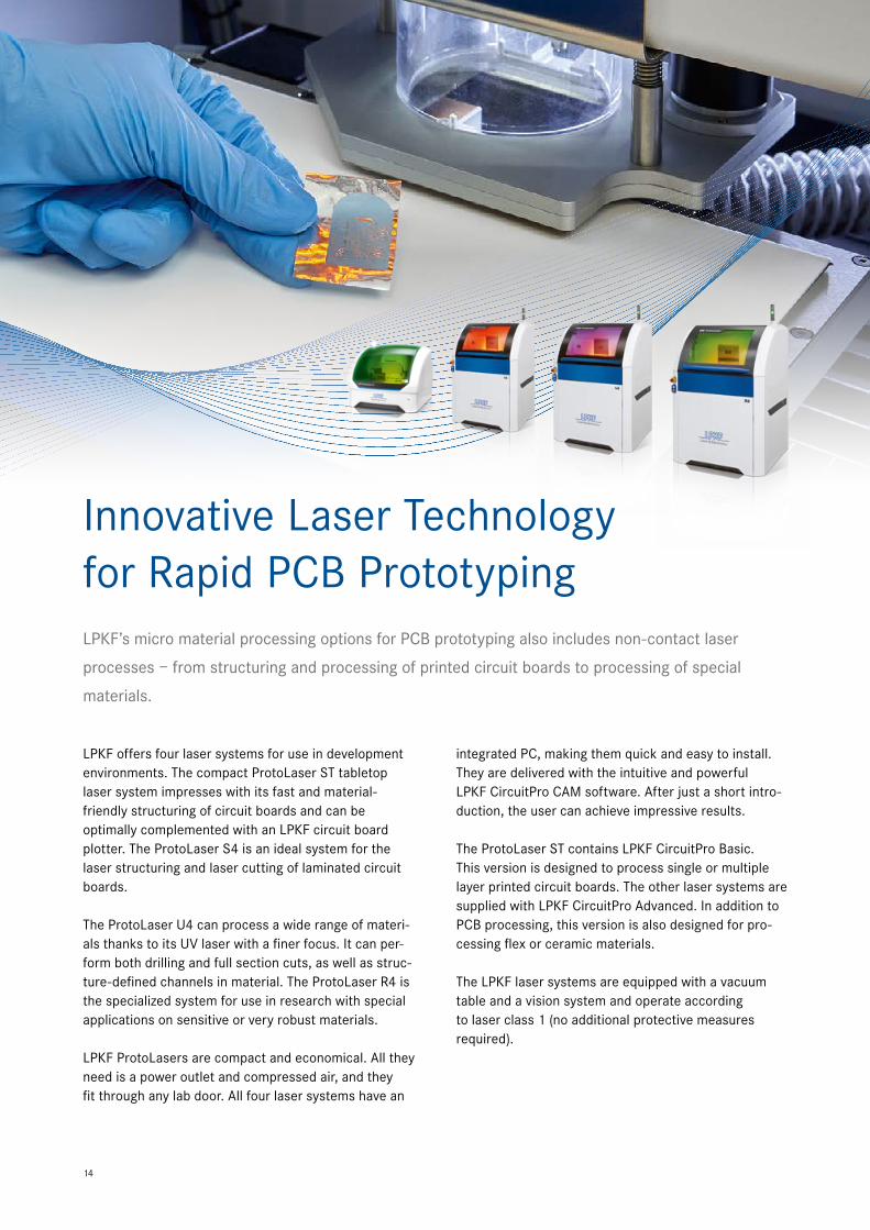
LPKF offers four laser systems for use in development environments. The compact ProtoLaser ST tabletop laser system impresses with its fast and material-friendly structuring of circuit boards and can be optimally complemented with an LPKF circuit board plotter. The ProtoLaser S4 is an ideal system for the laser structuring and laser cutting of laminated circuit boards.
The ProtoLaser U4 can process a wide range of materi-als thanks to its UV laser with a finer focus. It can per-form both drilling and full section cuts, as well as struc-ture-defined channels in material. The ProtoLaser R4 is the specialized system for use in research with special applications on sensitive or very robust materials.
LPKF ProtoLasers are compact and economical. All they need is a power outlet and compressed air, and they fit through any lab door. All four laser systems have an
LPKF’s micro material processing options for PCB prototyping also includes non-contact laser
processes – from structuring and processing of printed circuit boards to processing of special
materials.
integrated PC, making them quick and easy to install. They are delivered with the intuitive and powerful LPKF CircuitPro CAM software. After just a short intro-duction, the user can achieve impressive results.
The ProtoLaser ST contains LPKF CircuitPro Basic. This version is designed to process single or multiple layer printed circuit boards. The other laser systems are supplied with LPKF CircuitPro Advanced. In addition to PCB processing, this version is also designed for pro-cessing flex or ceramic materials.
The LPKF laser systems are equipped with a vacuum table and a vision system and operate according to laser class 1 (no additional protective measures required).
Innovative Laser Technology for Rapid PCB Prototyping

15
Laser processes offer numerous advantages over mechanical processes. The laser beam works in
a non-contact manner without generating any mechanical forces on the material being processed.
Laser Micro Material Processing
Laser systems are perfect for structuring circuit boards. A suitable selection of the laser wavelength as well as process control mean that the structuring can be adapted to numerous materials with various absorp-tion rates. This allows for the processing of standard as well as irregular material combinations, and prevent substrate damage.
Laser systems allow for cutting channels up to the mini-mum width of 15 μm. This precision is an advantage especially with corner radii and steep cutting edges, which speaks for the laser’s suitability for RF applica-tions. The structuring of circuit boards with laser sys-tems is similar to mechanical milling: The laser beam removes copper without residue thus creating isola-tion channels and conducting paths. The results are highly convincing with their sharp edges and precise geometries.
A process patented by LPKF ensures the clearing of large copper surfaces: The laser cuts the surface into thin stripes and dissolves them by heating the organic substrate. This process reduces the processing time drastically.
LPKF ProtoLaser S4 and U4 can cut common circuit board materials. Precise complete cuts through thin materials are possible. The laser tool is also highly convincing when cutting and drilling through rigid-flex circuit boards. In case of thicker materials, breakout tabs support the effectiveness of the laser process.
ProtoLaser R4 has proven extremely advantageous in the processing of micro materials. Its very short laser pulses mean that the heat input into the processed material can be controlled precisely. This allows for fine structures in thermally very sensitive materials.

16
Direct exposure of resists (ultrafine
conductor production)
Processing of thin flexible material
Processing of ceramics-filled materials
PCB reworking
Processing of fired ceramic
Processing of PTFE-filled materials
Processing of solder mask openings
Cutting of mounting holes
Processing of FR4 circuit boards
Processing of flexible and foil materials
Laser Applications

17
LPKF ProtoLaser ST (Part no.: 10090128)
Max. layout area and material size (X/Y/Z) 229 mm x 305 mm x 7 mm (9” x 12” x 0,28”)
Laser wavelength 1064 nm
Max. laser power 16 W
Laser pulse frequency 25 – 400 kHz
Diameter of focused laser beam 20 ± 2 μm (0.78 ± 0.08 Mil)
Structuring speed 8.5 cm2/min (1.3 in2/min)a on laminated substrates 18 μm (0.5 oz) Cu
Minimum line/space 100 μm / 50 μm (3.9 mil / 2 mil)a on FR4 18 μm (0.5 oz) Cu
Positioning accuracy in the scan field ± 10 μm (± 0.39 mil)
Repeatability in the scan field ± 1.8 μm (± 0.07 mil)
Dimensions (W x H x D) 725 mm x 665 mm x 840 mm (28.6” x 26.2” x 33.1”)
Weight 115 kg (254 lbs)
Power supply 115 – 230 V, 50 – 60 Hz, 500 W
Compressed air supply Min. 6 bar; 20 l/min (min. 87 PSI; 20 l/min)
Cooling Air-cooled
Ambient temperature; humidity 22 °C ± 2 °C (71.6 °F ± 4 °F); < 60 %
Software (starting on p. 21) LPKF CircuitPro Basic
Options and accessories (starting on p. 25) Dust extraction unit, compressor, starter set Tech
nica
l spe
cific
atio
ns s
ubje
ct to
cha
nge.
www.lpkf.com/protolaser-st
• Quick surface processing on all common circuit board materials
• Exact geometries by means of a contactless, scanner-based process
• Compact as a tabletop system and safe: lab-ready, laser class 1
• Intelligent, intuitive system software LPKF CircuitPro Basic
LPKF ProtoLaser ST – Tabletop System for Laser Structuring of PCBs
a Depending on material and laser beam parameters
The upgrade for your lab: Surfaces can be processed safely, precisely and suitably for the material with the compact LPKF ProtoLaser ST meaning that laser-structured circuit boards with exact geometries can be manufactured in only a few minutes. This is possible due to the combination of a better cutting capacity and a higher cutting speed. The safe lab system for the processing of FR4 and sensible RF materials will convince you with its amazing performance. Due to its compact tabletop format it can be used in any lab.
LPKF ProtoLaser ST allows for efficient prototyping of complex digital and analogue circuits, RF and microwave circuit boards. Without any tool wear, the laser system also processes demanding materials, and is ideally suited for the structuring of single- or double-sided laminated materials. Even flexible materials and foils can be freely positioned and exactly fixed.
The latest generation of the CAM and machine software CircuitPro Basic has been adapted to the further pro-cessing of drilled and cut-out circuit boards. The soft-ware and the integrated camera system allow for exact positioning. For operation, the compact table laser system requires only a power plug and compressed air.

18
Tech
nica
l spe
cific
atio
ns s
ubje
ct to
cha
nge.
www.lpkf.com/protolaser-s4
• Surface processing, suitable for the circuit, precise full section cuts and drill holes
• Compact and safe: lab-ready• Optimized for circuit board materials from
the electroplating process• Prototyping and on-demand processing
of custom small batches
LPKF ProtoLaser S4 – Laser Processing of PCBs
With the LPKF ProtoLaser S4, only a couple of minutes are needed from the layout to a structured circuit board – with exact geometries and drill holes for through-hole plating or cutouts. ProtoLaser S4 uses a laser source (532 nm, green) that, despite its high cutting capacity for copper, places hardly any stress on the substrate. Therefore, this lab laser can also safely process copper surfaces with inhomogeneities of up to 6 μm and is also suitable for the production of galvanic through-hole plating circuit boards as well as multilayer components. Fast processing, a wide choice of materials, safe pro-cess results in the lab!
ProtoLaser S4 is a solution for efficient prototyping of complex digital and analogue circuits, RF and microwave circuit boards with a size of up to 229 mm x 305 mm (9” x 12”). It is ideal for the production of single- or double-sided circuit boards, antennas, filters, and numerous applications featuring precise, steep flanks. In addition, it provides exact geometries on technical ceramic materials.
This laser system features the Advanced version of the LPKF CircuitPro software, which boasts various handy extras in addition to the necessary features (see page 21).
a Depending on material and laser beam parametersb Height with open hood: 1765 mm (69.5”)
LPKF ProtoLaser S4 (Part no.: 10055359)
Max. layout area (X/Y/Z) 229 mm x 305 mm x 7 mm (9” x 12” x 0.28”)
Max. material size (X/Y/Z) 239 mm x 315 mm x 7 mm (9.4” x 12.4” x 0.28”)
Laser wavelength 532 nm
Max. laser power 12 W
Laser pulse frequency 25 – 300 kHz
Diameter of focused laser beam 20 ± 2 μm (0.78 ± 0.08 mil)
Structuring speed 12 cm2/min (1.9 in2/min)a on laminated substrates 18 μm (0.5 oz) Cu
Minimum line/space 75 μm / 25 μm (2.9 mil / 2.9 mil)a on FR4 18 μm (0.5 oz) Cu
Positioning accuracy in the scan field ± 10 μm (± 0.39 mil)
Repeatability in the scan field ± 2.2 μm (± 0.09 mil)
Dimensions (W x H x D) 910 mm x 1650 mm x 795 mm (35.8” x 64.9” x 31.3”)b
Weight 350 kg (772 lbs)
Power supply 110 – 230 V, 50 – 60 Hz, 1.5 kW
Compressed air supply Min. 6 bar; 185 l/min (min 87 psi; 185 l/min)
Cooling Air-cooled (internal cooling cycle)
Ambient temperature; humidity 22 °C ± 2 °C (71.6 °F ± 4 °F); < 60 %
Software (starting on p. 21) LPKF CircuitPro Advanced
Options and accessories (starting on p. 25) Dust extraction unit, compressor, starter set

19
LPKF ProtoLaser U4 – Multipurpose Tool for the Electronics Lab
One System, Multiple ApplicationsThe LPKF ProtoLaser U4 with integrated UV laser is capable of processing a wide variety of materials. It is easy to install and even easier to use. The high pulse energy of the UV laser leads to a residue-free ablation process, resulting in geometrically precise contours.
The LPKF ProtoLaser U4 can structure or cut diverse materials quickly and cleanly. The laser wavelength used makes the UV laser a truly multifunctional tool. A UV laser beam can cut individual boards out of large boards with high precision and no stress, drill holes and microvias, and create openings in solder masks. It can cut and structure LTCCs, fired ceramics, ITO/TCOsubstrates, delicate prepregs, and laminated materials.
The processing of various materials is supported by the CircuitPro Advanced software. An extensive materials library supplies the laser parameters for key materials. Because the ProtoLaser U4 works without material contact, tooling costs are a thing of the past. Micro material processing thus benefits from the fine laser beam diameter, the extremely precise focusing along the Z-axis, and the exact control of the processing positions.
Tech
nica
l spe
cific
atio
ns s
ubje
ct to
cha
nge.
www.lpkf.com/protolaser-u4
a Depending on material and laser beam parametersb Height with open hood: 1765 mm (69.5”)
LPKF ProtoLaser U4 (Part no.: 10055358)
Max. layout area (X/Y/Z) 229 mm x 305 mm x 7 mm (9” x 12” x 0.28”)
Max. material size (X/Y/Z) 239 mm x 315 mm x 7 mm (9.4” x 12.4” x 0.28”)
Laser wavelength 355 nm
Max. laser power 5.7 W
Laser pulse frequency 25 – 300 kHz
Diameter of focused laser beam 20 ± 2 μm (0.78 ± 0.08 mil)
Structuring speed 5.5 cm2/min (0.9 in2/min)a on laminated substrates 18 μm (0.5 oz) Cu
Minimum line/space 50 μm / 20 μm (20 mil / 0.8 mil)a on FR4 18 μm (0.5 oz) Cu
Positioning accuracy in the scan field ± 10 μm (± 0.39 mil)
Repeatability in the scan field ± 2.2 μm (± 0.09 mil)
Dimensions (W x H x D) 910 mm x 1650 mm x 795 mm (35.8” x 64.9” x 31.3”)b
Weight 350 kg (772 lbs)
Power supply 110 – 230 V, 50 – 60 Hz, 1.5 kW
Compressed air supply Min. 6 bar; 185 l/min (min 87 psi; 185 l/min)
Cooling Air-cooled (internal cooling cycle)
Ambient temperature; humidity 22 °C ± 2 °C (71.6 °F ± 4 °F); < 60 %
Software (starting on p. 21) LPKF CircuitPro Advanced
Options and accessories (starting on p. 25) Dust extraction unit, compressor, starter set
• Excellent quality and high material variety due to the UV laser wavelength
• Laser-stabilized in the low energy area for the processing of thin and sensible materials
• Power measurement on the substrate level for process control
• Compact and safe: lab-ready

20 www.lpkf.com/protolaser-r4
An important parameter for laser micro-processing is the pulse duration. The LPKF ProtoLaser R4 with picosecond-short laser pulses allows the high-precision structuring of sensitive substrates, as well as the cutting of hardened or fired substrates.
Laser Ablation with Virtually No Heat InputThe shorter the processing pulse, the lower the heat input into the adjacent material. With the picosecond laser, there is practically no heat transfer, the material vaporises directly.
Micro Material Processing at its BestThis thermal effect is important for the cutting and surface processing of temperature-sensitive materials. The laser offers very high pulse energy for cutting, for example, ceramic materials such as Al
2O
3 or GaN
without discoloring them in the processing procedure. Due to the low heat input, no micro-cracks occur in the material.
The ProtoLaser R4 is also the perfect system for surface processing – such as ablating transparent thin films or removing metal layers from plastic foils. It achieves the targeted very stable laser input at low laser power. This allows standard FR4 and laminated RF materials to be processed just as well.
• Precision picosecond laser for innovative research
• Gentle processing of thermally sensitive materials
• Intuitive CAM software• Ready-to-use laser class 1 lab system
LPKF ProtoLaser R4 – Specialist for Material-friendly Processing
The high-precision hardware and integrated camera are supported by the easy-to-use LPKF CircuitPro software. This enables the user to implement projects involving demanding materials in their own laboratory within a very short time.
a Depending on material and laser beam parametersb Height with open hood: 1765 mm (69.5”)
Tech
nica
l spe
cific
atio
ns s
ubje
ct to
cha
nge.
LPKF ProtoLaser R4 (Part no.: 10099642)
Max. layout area (X/Y/Z) 229 mm x 305 mm x 7 mm (9” x 12” x 0.28”)
Max. material size (X/Y/Z) 239 mm x 315 mm x 7 mm (9.4” x 12.4” x 0.28”)
Laser wavelength 515 nm
Max. laser power 8 W
Laser pulse frequency 50 – 500 kHz
Diameter of focused laser beam 15 ± 2 μm (0.59 ± 0.08 Mil)
Structuring speed 5.5 cm2/min (0.9 in2/min)a on laminated substrates 18 μm (0.5 oz) Cu
Laser pulse length 1.5 ps
Minimum line/space 35 μm / 20 μm (1.38 mil / 0.79 mil)a on FR4 18 μm (0.5 oz) Cu
Positioning accuracy in the scan field ± 5 μm (± 0.2 Mil)
Repeatability in the scan field ± 0.23 μm (± 0.009 Mil)
Dimensions (W x H x D) 910 mm x 1650 mm x 795 mm (35.8” x 64.9” x 31.3”)b
Weight 390 kg (860 lbs)
Power supply 110 – 230 V, 50 – 60 Hz, 2 kW
Compressed air supply Min. 6 bar; 185 l/min (min 87 psi; 185 l/min)
Cooling Air-cooled (internal cooling cycle)
Ambient temperature; humidity 22 °C ± 2 °C (71.6 °F ± 4 °F); < 60 %
Software (starting on p. 21) LPKF CircuitPro Advanced
Options and accessories (starting on p. 25) Dust extraction unit, compressor, starter set

21
LPKF CircuitPro – Smart Software with Intuitive OperationLPKF ProtoMat circuit board plotters and ProtoLaser systems are equipped with the powerful
LPKF CircuitPro system software. The software is easy to use and intuitive and has a high degree
of flexibility for optimum support even in the complex processing of innovative materials.
LPKF CircuitPro enables the easy creation of printed circuit boards in the shortest possible time. Data can be easily imported from any common design software. Application-dependent templates and predefined work sequences make using the application a breeze. The user makes the selection, the software generates the individual processing steps from it and prepares the production data.
LPKF CircuitPro then guides the user through the manufacturing process step by step.
The intuitive menu navigation makes LPKF CircuitPro very easy to understand without special training and is therefore suitable for occasional applications.

22
Also and Especially for Special ApplicationsIn research and development especially, new mate-rial compositions are often used or applications that require very specific layouts. LPKF CircuitPro has extensive functions for drawing or manipulating (adjust-ing) the data, as well as various parameter search func-tions or parameter settings. The software thus enables rapid and reproducible progress with even highly inno-vative projects and materials.
Thanks to the adjustable user levels, research and train-ing projects and near-series prototyping are optimally supported. LPKF CircuitPro controls the systems largely independently and informs the user by e-mail about any necessary interventions in the processing procedure – for example, the upcoming turning of the base material.
Through Experience to Simple ProcessesWith many years of experience in PCB prototyping and in processing new materials from the electronics sec-tor, LPKF CircuitPro has been developed to best suit in-house prototyping.• The automatic import of CAD data can be easily
adapted to the established workflow through a one-time adaptation to existing file name suffixes.
• Sophisticated routines for milling or laser path calculation guarantee fast, optimal and reproducible results. The calculation is specifically adapted to the material chosen by the user for the project at hand.
• The extensive templates and models have also been developed based on customer feedback on specific requirements from research and industry. Example: optimized calculation routines for applications in high-frequency technology, which are specifically designed for optimum sharp edges and the homogeneous removal of material on the surface.
• Extensive draw-and-edit functions offer the possibil-ity to create small adjustments or test layouts quickly and directly in the system without having to generate new data in CAM.
A great deal of experience has also gone into the rou-tines developed by LPKF for material processing with the laser. The wide variety of calculation models that have been developed over the years enable very fast material ablation, as well as the processing of the thin-nest material layers without damaging the underlying substrates.
Six Steps to a Finished Printed Circuit Board
1. Create a circuit diagram in a CAD program
2. Create PCB design data in the CAD program, e. g. in Gerber or DXF format
3. The intuitive import of design data into predefined templates in LPKF CircuitPro
4. The automatic calculation of the milling or laser paths depending on the selected strategy
5. The template-dependent assign-ment of drill diameter, position and technology: simple through-holes, holes for vias, blind or buried vias for multilayer applications.
6. Calculation of the user-selected strategy for depaneling.

23
The Advantages of CircuitPro• The intuitive operator guidance leads the user through
the manufacturing process depending on the template selected and the material used.
• The software “thinks” along with you: If intermediate steps are required, such as through-hole plating or pressing several layers together to form a multilayer board, LPKF CircuitPro will inform the user. The soft-ware later resumes the process at the exact location and automatically starts reading the fiducials on the PCB.
• LPKF CircuitPro uses the integrated camera, which is standard equipment in all LPKF systems, to precisely read the material position and measure the milled or laser cuts created.
• The fully automatic tool change of the LPKF ProtoMat and the associated milling width adjustment are sup-ported by LPKF CircuitPro.
• All the materials research possibilities for experienced users: The software contains numerous templates in which the process sequence or the processing of individual areas of the layout can easily be manually adjusted. For the laser tools especially, it is very easy for the user to create new tool libraries based on the generated results for a specific material.
• LPKF CircuitPro also generates templates for solder stop masks and legend printing, which can easily be applied to the PCB material with additional LPKF equipment.
• For LPKF ProtoMats equipped with a dispensing unit, CircuitPro also creates the dispensing positions and the processing sequence for applying the solder paste.
Flexible and Completely as Desired: Basic or Advanced VersionTo optimally support the customer’s application, LPKF offers the LPKF CircuitPro software in Basic or Advanced versions. LPKF CircuitPro Basic is included with all LPKF ProtoMat and LPKF ProtoLaser systems and fully supports data preparation and the production of double-sided PCB prototypes.
LPKF CircuitPro Advanced accommodates a wide range of users with various extra functions:
• Additional import of the DXF format • Advanced isolation function • Additional templates for up to 8 layers in multilayer
structures• 2.5D function, for example to produce housing parts
or front panels using LPKF ProtoMat systems with Z-axis control
• An additional calculation routine that is used especially when processing flexible materials or technical ceramics
• Extended “Step and Repeat” function for the production of small batches
• The import and editing of multiple different files in one dataset
A free four-week demo version of the LPKF CircuitPro software is available at the LPKF website at: www.lpkf.com/software-download

24
Function Description
Import FormatsGerber Standard (RS-274-D), Extended Gerber (RS-274-X), Gerber X2, Excellon NC Drill (Version 1 and 2), Sieb & Meier NC Drill, HP-GL™, DPF, Auto-CAD™ DXF*, IGES, LMD, STEP, CP2D
Editing FunctionsMove Object, Rotate, Mirror, Scale/Expand, Difference/Merge, Split, Round/Chamfer, Fill/Contour, Path Manipulation, Modify Flash, Group Function, Convert Polygon, Convert Flash
Graphic FunctionsFlash, Path, Polygon, Rectangle or Rectangle Path, Circle or Circle Path, Text, Data Matrix Code, Fiducial
Insulation Methods
Insulation with a single insolation channel, single insolation channel with double channel for pads, partial milling out of large insulation areas (rub-out) with removal of copper in defeated areas*, complete milling/laser processing out of large insulation areas (rub-out), milling with concentric- x-serpentine or y-serpentine strategy, RF insolation strategy, laser with rub-out process or hatch only strategy, additional multiple insulation of pads, removal of residual copper spikes (spike option), minimum insulation spaces
Special Functions
Routing path generator with or without breakout tabs, Free placement of taps, Insulation width adjustment, Pad insolation width adjustment, 2.5D data generation*, Z-depth penetration adjustment, optimized automatic scan field generation, manual scan field order setting, scanfield work order meander/spiral selection check copper thickness, snap and grid function, volume operations, joining/separating objects, step & repeat, ground plane, generation with defined clearance, perform inner insolation, replace existing tool path, pockets and blind via assignment
Display Functions
Separate zoom window (freely definable), zoom in/out, overview, redraw, individual layers selectable/visible, panning (keyboard), layer in solid/outline/center line display, camera view with measure function, different colors for tracks and pads of the same layer, different colors for insulation toolszoom in/out/working area/projects, previous view, all viewing methods available at all times, even during the machining process, graphical display of the current head position
Marker FunctionsSingle element, total layer, all layers, pad groups, selection and limiting to specific layers possible for lines/polygons/circles/rectangles/pads/holes (multiple choice and restriction to specific layers possible)
Graphic FunctionsLines (open/closed), circle, polygon, rectangle, pad, hole, text, flash, tool path, workflow, work package options
Control Functions Measuring, design rule check, aperture list library
ControlProtoMat circuit board plotters and ProtoLaser; Process all, stop processing, add production phase, select head/camera, laser pointer, illumination working area, vacuum remote, home position, pause position, load position, zero position, move x,y,z by free definite able steps or by cursor
Placement Functions Copy, move, step and repeat, handles multiple artworks and placements simultaneously
Selection MethodsTotal production phase, specific tools, individual drill holes/lines/segments, tool pathes, hole/line segment, dynamic highlighting
Tool ManagementMilling: feed speed, rotation speed, max tool life, max penetration depth, z penetration depth, diameterLaser: frequency, power, mark speed, focus offset, repetitions, delay, compressed air support, beam diameter, laser on/off delay, jump settings, minimum angel, THP settings
Tool Library Unlimited, individual library for different material types, individual customizable parameters
Programming Material Size Positioning with corner coordinates, with the mouse, camera, direct coordinates
OtherProgramable mailing information about process status, production time and calculation time status bar, integration of a camera option with automatic fiducial recognition, check for broken tools
Supported LanguagesEnglish, German, French, Spanish, Italian, Chinese, Japanese, Slovenian, Polish, Russian, Swedish, Suomi, Portuguese
Basic version supplied with ProtoMat E44, ProtoMat S64, ProtoLaser ST
Advanced version supplied with ProtoMat S104, ProtoLaser S4, ProtoLaser U4, ProtoLaser R4
Supported LPKF systemsProtoMat: S104, S64, S103, S63, S43, S100, S62, S42, H60, H100ProtoLaser: S, U, U3, S4, U4, ST, R, R4
Functions of the LPKF CircuitPro System Software
* only LPKF CircuitPro Advanced

25
The performance capabilities of the LPKF circuit board plotters and ProtoLasers can be extended
through the addition of accessories and options. High-grade materials and precision workmanship
ensure the high reliability and longevity of all add-ons. The accessories can easily be installed in
existing systems without the help of specialists.
Accessories for LPKF Circuit Board Plotters and ProtoLasers
Dust Extraction UnitThe LPKF dust extraction unit with absolute filter eliminates fibers, chips, and fine dust. The integrated AutoSwitch function switches the dust extraction unit on and off automatically.
Dust Extraction Unit ProtoMat S + E ProtoLaser
Part no. 10033243 124391
Vacuum pressure Max. 22 500 Pa Max. 21 000 Pa
Air flow rate 241 m3/h (142 cfm) 320 m3/h (188 cfm)
Power consumption800 W (230 V) or 960 W (120 V)
1.6 kW (230 V, 50/60 Hz)
Dimensions (W x H x D)
250 mm x 300 mm x 350 mm (10” x 12” x 14”)
365 mm x 1245 mm x 501 mm(14.4” x 49” x 19.7”)
Acoustic pressure 50 dB(A) Ca. 65 dB(A)
Absolute filter HEPA filter HEPA filter
Remote control Software-controlled Software-controlled
Technical specifications subject to change.
26 Technical specifications subject to change.
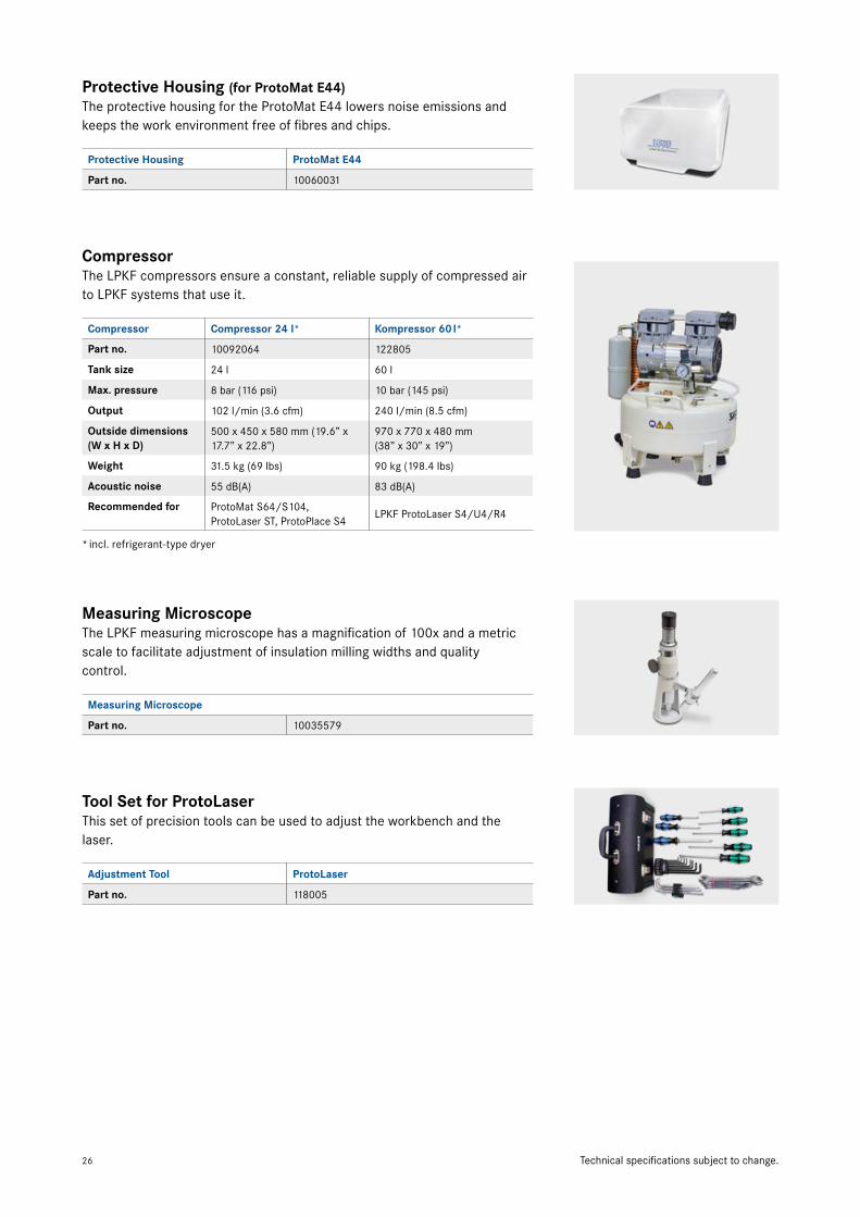
Measuring MicroscopeThe LPKF measuring microscope has a magnification of 100x and a metric scale to facilitate adjustment of insulation milling widths and quality control.
Measuring Microscope
Part no. 10035579
Tool Set for ProtoLaserThis set of precision tools can be used to adjust the workbench and the laser.
Adjustment Tool ProtoLaser
Part no. 118005
* incl. refrigerant-type dryer
Protective Housing ProtoMat E44
Part no. 10060031
CompressorThe LPKF compressors ensure a constant, reliable supply of compressed airto LPKF systems that use it.
Compressor Compressor 24 l* Kompressor 60 l*
Part no. 10092064 122805
Tank size 24 l 60 l
Max. pressure 8 bar (116 psi) 10 bar (145 psi)
Output 102 l/min (3.6 cfm) 240 l/min (8.5 cfm)
Outside dimensions (W x H x D)
500 x 450 x 580 mm (19.6” x 17.7” x 22.8”)
970 x 770 x 480 mm(38” x 30” x 19”)
Weight 31.5 kg (69 lbs) 90 kg (198.4 lbs)
Acoustic noise 55 dB(A) 83 dB(A)
Recommended for ProtoMat S64/S104, ProtoLaser ST, ProtoPlace S4
LPKF ProtoLaser S4/U4/R4
Protective Housing (for ProtoMat E44)The protective housing for the ProtoMat E44 lowers noise emissions and keeps the work environment free of fibres and chips.

27Technical specifications subject to change.
Tool Holder Extension Set for the LPKF ProtoMat S64Five additional tool holders for mounting on the machinework table incl. software upgrade.
Tool Holder Extension Set for the LPKF ProtoMat S64
Part no. SET-10-1163N
Accessories for LPKF ProtoMat Sx4
Status Light for the ProtoMat Sx4On the machine housing, it display the status: Operation, fault, user inter-vention required.
Status Light for the ProtoMat Sx4
Part no. 10035540
Dispenser Set for the ProtoMat Sx4Contains a holder for the solder paste cartridge and a size 27 dispensing needle.
Dispenser Set for the ProtoMat Sx4
Part no. 10098906

28
Copper-clad FR4 Base Materials (thickness of 1.5 mm, 10 per package)Unless otherwise specified, the base materials are shipped with dimensions 229 mm x 305 mm (9” x 12”).Without 3 mm registration holes.
Part no. Description
112060N Base material FR4, A4, 5/5 μm, 1.5 mm thickness (NPB) with Cu protection film, set of 10
106394N Base material FR4, A4, 18/18 μm, 1.5 mm thickness (NPB), set of 10
106396N Base material FR4, A4, 0/35 μm, 1.5 mm thickness (NPB), set of 10
106397N Base material FR4, A4, 35/35 μm, 1.5 mm thickness, set of 10
112059N Base material FR4, A3, 5/5 μm, 1.5 mm thickness (NPB) with Cu protection film, set of 10
106398N Base material FR4, A3, 18/18 μm, 1.5 mm thickness (NPB), set of 10
106400N Base material FR4, A3, 0/35 μm, 1.5 mm thickness (NPB), set of 10
106401N Base material FR4, A3, 35/35 μm, 1.5 mm thickness (NPB), set of 10
Technical specifications subject to change.
LPKF supplies high-quality consumables – from copper-clad base materials to cleaning pads and
special adhesive tape, LPKF guarantees first-class product quality.
Operating Materials for LPKF Circuit Board Plotters and LPKF Laser Systems

29
Multilayer Sets
Part no. Description
121093 6-layer multilayer set for MultiPress S, electroplating with H and S series
121102 4-layer multilayer set for MultiPress S, ProConduct with H and S series
121103 4-layer multilayer set for MultiPress S, electroplating with H and S series
124481 8-layer multilayer set for MultiPress S, (NPB) electroplating with H and S series
100985534-layer multilayer set for blind/buried via (excl. ProtoMat S64/S104), size of the base material: 235 mm x 305 mm (9.25” x 12”) base and auxiliary material for 10 multilayers
100985574-layer multilayer set for blind/buried via (excl. ProtoLaser S4/U4/R4 or combination ProtoMat & ProtoLaser), size of the base material: 235 mm x 305 mm (9,25” x 12”)
100985586-layer multilayer set for blind/buried via (excl. ProtoLaser S4/U4/R4 or combination ProtoMat & ProtoLaser), size of the base material: 235 mm x 305 mm (9,25” x 12”)
100985596-layer multilayer set for blind/buried via (excl. ProtoMat S64/S104), size of the base material: 235 mm x 305 mm (9.25” x 12”) base and auxiliary material for 10 multilayers
100985608-layer multilayer set for blind/buried via (excl. ProtoLaser S4/U4/R4 or combination ProtoMat & ProtoLaser), size of the base material: 235 mm x 305 mm (9,25” x 12”)
100985618-layer multilayer set for blind/buried via (excl. ProtoMat S64/S104), size of the base material: 235 mm x 305 mm (9.25” x 12”) base and auxiliary material for 10 multilayers
Part no. Description
SET-10-1053NBase material FR4, 229 mm x 305 mm (9” x 12”), 5/5 μm with Cu protective foil, thickness 1.5 mm, pre-drilled with 3 mm fitting holes, set of 10
115968N Base material FR4, 229 mm x 305 mm (9” x 12”), (NPB) 0/18 μm, thickness 1.5 mm, pre-drilled with 3 mm fitting holes, set of 10
SET-10-1118NBase material FR4, 229 mm x 305 mm (9” x 12”), (NPB) 0/18 μm, thickness 1.5 mm, pre-drilled with 3 mm fitting holes, set of 10, made in China
115967N Base material FR4, 229 mm x 305 mm (9” x 12”), (NPB) 18/18 μm, thickness 1.5 mm, pre-drilled with 3 mm fitting holes, set of 10
SET-10-1119NBase material FR4, 229 mm x 305 mm (9” x 12”), (NPB) 18/18 μm, thickness 1.5 mm, pre-drilled with 3 mm fitting holes, set of 10, made in China
SET-10-1001N Base material FR4, 229 mm x 305 mm (9” x 12”), (NPB) 0/35 μm, thickness 1.5 mm, pre-drilled with 3 mm fitting holes, set of 10
SET-10-1116NBase material FR4, 229 mm x 305 mm (9” x 12”), (NPB) 0/35 μm, thickness 1.5 mm, pre-drilled with 3 mm fitting holes, set of 10, made in China
SET-10-1000N Base material FR4, 229 mm x 305 mm (9” x 12”), (NPB) 35/35 μm, thickness 1.5 mm, pre-drilled with 3 mm fitting holes, set of 10
SET-10-1117NBase material FR4, 229 mm x 305 mm (9” x 12”), (NPB) 35/35 μm, thickness 1.5 mm, pre-drilled with 3 mm fitting holes, set of 10, made in China
Copper-clad FR4 Base Materials (thickness of 1.5 mm, 10 per package)Unless otherwise specified, the base materials are shipped with dimensions 229 mm x 305 mm (9” x 12”).
Drill Underlay SheetsDrill underlay sheets are used as backing for the base materials to prevent damage to the machine table.
Part no. Description Sheets per Package
SET-10-1086 N Drill underlay sheet, DIN A4, d = 2 mm 10
SET-10-1052 N Drill underlay sheet (predrilled), 229 mm x 305 mm (9” x 12”), d = 2 mm 10
Technical specifications subject to change.
30
Part no. Description Pads per Package
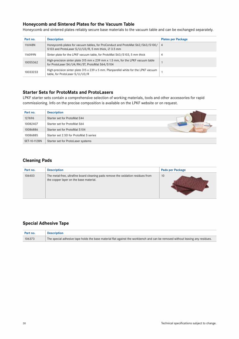
106403 The metal-free, ultrafine board cleaning pads remove the oxidation residues from the copper layer on the base material.
10
Special Adhesive Tape
Part no. Description
106373 The special adhesive tape holds the base material flat against the workbench and can be removed without leaving any residues.
Cleaning Pads
Technical specifications subject to change.
Part no. Description
127696 Starter set for ProtoMat E44
10082407 Starter set for ProtoMat S64
10086886 Starter set for ProtoMat S104
10086885 Starter set 2.5D for ProtoMat S series
SET-10-1128N Starter set for ProtoLaser systems
Starter Sets for ProtoMats and ProtoLasersLPKF starter sets contain a comprehensive selection of working materials, tools and other accessories for rapid commissioning. Info on the precise composition is available on the LPKF website or on request.
Honeycomb and Sintered Plates for the Vacuum TableHoneycomb and sintered plates reliably secure base materials to the vacuum table and can be exchanged separately.
Part no. Description Plates per Package
116148N Honeycomb plates for vacuum tables, for ProConduct and ProtoMat S62/S63/S100/S103 and ProtoLaser S/U/U3/R, 5 mm thick, ∅ 3.5 mm
4
116099N Sinter plate for the LPKF vacuum table, for ProtoMat S63/S103, 5 mm thick 4
10055362High-precision sinter plate 315 mm x 239 mm x 1.5 mm, for the LPKF vacuum table for ProtoLaser S4/U4/R4/ST, ProtoMat S64/S104
1
10033233High-precision sinter plate 315 x 239 x 5 mm. Planparellel white for the LPKF vacuum table, for ProtoLaser S/U/U3/R
1

31
LPKF Drilling and Milling Tools for LPKF ProtoMatsLPKF places high demands on every single tool. The drilling and milling tools developed especially
for LPKF are high-quality hard metal tools. They guarantee a long service life, precise structures,
and cleanly milled edges.
The tools are divided into two main categories: surface tools with a total length of 36 mm (1.42”) for surface machining (cutters and end mills) and through-thickness tools with a total length of 38 mm (1.5”) for penetrating the base material (spiral drills, contour routers, and end mills).
Starter Toolbox 1/8” Shaft with Distance Rings (Part no. 129103)For all LPKF ProtoMat models. Includes tools with pressed-on distance rings: various universal cutters, microcutters, end mills, contour routers, and spiral drills in a handy toolbox.
RF and Microwave Starter Toolbox with Distance Rings (Part no. 116394)Supplements the toolkit with 20 special RF end mill tools.

32
Part no. Length/Milling Width Description
Microcutter/fine-line milling tool 1/8”, conical, orange distance ring, 36 mm
115836 0.10 – 0.15 mm (4 – 6 mil) For fine insulation spacings with a Cu thickness of 18 μm
Universal cutter 1/8”, conical, orange distance ring, 36 mm
115835 0.2 – 0.5 mm (8 – 20 mil) For milling of different insulation spacings in copper-coated base material
End mill (RF) 1/8’’, cylindrical, blue distance ring, 36 mm
115832 d = 0.15 mm (6 mil) For minimal insulation spacings in RF applications
115833 d = 0.25 mm (10 mil)
115834 d = 0.40 mm (16 mil)
End mill 1/8’’, cylindrical, violet distance ring, 36 mm
115839 d = 0.80 mm (31 mil) For wide insulation spacings and engraving of aluminum front panels and cutouts
115840 d = 1.00 mm (39 mil)
129100* d = 2.00 mm (79 mil)
129101* d = 3.00 mm (118 mil)
End mill long 1/8’’, cylindrical, light green distance ring, 38 mm
115837 d = 1.00 mm (39 mil) For milling of Al and contour milling of soft base materials for RF and microwave applications
129102* d = 2.00 mm (79 mil)
Contour router 1/8”, cylindrical, yellow distance ring, 38 mm
115844 d = 1.00 mm (39 mil) For milling of internal and external contours and drilled holes > 2.4 mm (> 94 mil)
129099* d = 2.00 mm (79 mil)
Spiral drill 1/8”, cylindrical, green distance ring, 38 mm
115846 d = 0.20 mm (8 mil) For drilled holes < 2.4 mm (< 94 mil)
115847 d = 0.30 mm (12 mil)
115848 d = 0.40 mm (16 mil)
115849 d = 0.50 mm (20 mil)
115850 d = 0.60 mm (24 mil)
115851 d = 0.70 mm (28 mil)
115852 d = 0.80 mm (31 mil)
115853 d = 0.85 mm (33 mil)
115854 d = 0.90 mm (35 mil)
115855 d = 1.00 mm (39 mil)
115856 d = 1.10 mm (43 mil)
115857 d = 1.20 mm (47 mil)
115858 d = 1.30 mm (51 mil)
115859 d = 1.40 mm (55 mil)
115860 d = 1.50 mm (59 mil)
115861 d = 1.60 mm (63 mil)
115862 d = 1.70 mm (67 mil)
115863 d = 1.80 mm (71 mil)
115864 d = 1.90 mm (75 mil)
115865 d = 2.00 mm (79 mil)
115866 d = 2.10 mm (83 mil)
115867 d = 2.20 mm (87 mil)
115868 d = 2.30 mm (91 mil)
115869 d = 2.40 mm (94 mil)
115870 d = 2.95 mm (116 mil)
115871 d = 3.00 mm (118 mil)
* Shaft 25 mm (984 mil)
Technical specifications subject to change.

33
Systems and Processes for Manufacturing Component PopulationAfter the printed circuit board has been manufactured, the prototyping process is not yet complete.
Only with the following processes – through-hole plating, solder resist, solder paste printing,
assembly and reflow soldering – a PCB becomes an electronic assembly.

34
LPKF EasyContac is a manual system for through-hole plating of double-sided PCBs with copper alloy rivets. The set includes 1000 rivets each of outside diameter 0.8 mm (32 mil), 1.0 mm (40 mil), 1.2 mm (48 mil), and 1.4 mm (56 mil), press tools, an anvil, and tweezers.
The contact resistance is 10 mΩ; the rivet system can be used for material thicknesses of up to about 1.5 mm (59 mil).
Part no.: 110914
Reliable through-hole plating without using a galvanic process! The paste-based through-hole plating method is also suitable for a large number of through holes with a minimum diameter of 0.4 mm (15 mil) and a maximum aspect ratio of 1:4.
The contact resistance is about 20 mΩ with a standard deviation of 8 mΩ. FR4, RF, and microwave materials (including PTFE-based materials) are suitable for contacting.
The procedure is simple:• First a protective film is adhered to each side of
the structured board• Then a LPKF ProtoMat drills the required holes
through the films and the board• With the help of a squeegee and a vacuum – the
vacuum tables on the ProtoMats are used for this purpose – the ProConduct paste is pulled through the holes on both sides
• The protective films are removed and the board is cured in the convection oven
LPKF ProConduct comes as a complete set with all tools, disposable gloves, protective films, and paste in portions with the required amounts.
• Easy and cost-effective• Comes complete with tool• Ideal for a small number of through holes
• No galvanic baths• Low-resistance, thermally stable plated
through holes• Quick and easy operation• Also suitable for PTFE and other challenging
substrates
Options and accessories (p. 43)Vacuum table, convection oven
LPKF EasyContac – Manual Through-Hole Plating of Double-Sided PCBs
LPKF ProConduct – Reliable Through-Hole Plating for PCB Prototyping with Conductive Paste
Part no. 115790
www.lpkf.com/proconduct

35
In galvanic through-hole plating, a very homogeneous copper layer is deposited over the entire surface of the base material and the inner walls of the through holes down to a minimum hole diameter of 0.2 mm (8 mil). The compact LPKF Contac S4 has six baths for reliably performing this task: all work steps from surface activation to the tin finish are integrated in a compact, low-maintenance unit.
The LPKF Contac S4 utilizes optimal designed anode plates and reverse pulse plating for especially uniform copper layer buildup. PCBs with through-hole plating accomplished in this way are also suitable, e. g., for structuring with the LPKF ProtoLaser S4.
The integrated computer with touch display assumes the operation and guides the user through each step of the metallization process.
The Contac S4 can also process multilayers with up to eight layers with a maximum aspect ratio of 1:10 (hole diameter to PCB thickness). A final tin bath step protects the surface and improves solderability. The long-lasting chemicals require little maintenance and have been developed and optimized specifically for the system.
• Uniform copper layer buildup• Reverse pulse plating (RPP), black hole
process, and microvia cleaning• Chemical (electroless) tin plating• Through-hole plating even for small
diameters of > 0.2 mm (> 8 mil)• No knowledge of chemistry required
LPKF Contac S4 (Part no.: 10055361)
Max. material size (X x Y) 230 mm x 330 mm (9.1” x 13”)
Max. layout area (X x Y) 200 mm x 300 mm (7.9” x 11.8”)
Reverse pulse plating Adjustable
Tolerance ± 2 μm (0.08 mil), copper coating
Minimum hole diameter ≥ 0.2 mm (0.8 mil)
ViaCleaner Integrated
Chemical tin plating Integrated
Process time Approx. 90 – 120 min
Power supply 90 – 240 V, 50 – 60 Hz, 0.6 kW
Dimensions (W x H x D) 856 mm x 446 mm x 542 mm (33.7” x 17.7” x 21.3”)
Options and accessories (p. 43) ViaCleaner chemical set, powder for electroless tin plating
LPKF Contac S4 – Table-Top Through-Hole Electroplating
Tech
nica
l spe
cific
atio
ns s
ubje
ct to
cha
nge.
www.lpkf.com/contac-s4

36
8-layer Multilayer in Your Own LabA high packing density and the correlated high number of circuits or additional tasks that need to be performed by the circuit board require the design of complex proto types as multilayer. They can accommo-date circuits in several layers.
LPKF MultiPress S is a tabletop system for pressing of multilayers in your own lab. The short process time of only approx. 90 minutes as well as user-friendly operation make the system an ideal tool for a safe production of multilayer prototypes as well as small batches.
LPKF MultiPress S presses complex circuit boards with up to eight layers in one step. Various pressure, temperature, and time profiles allow for top flexibility in the material selection and the number of layers. MultiPress S is available as the version with a manual hand pump or automatic hydraulics.
• In-house production of multilayer prototypes with rigid or flexible materials, RF materials
• Very short processing times and easy-to-use menu guidance
• Preset and individual process profiles• Automatic hydraulics
LPKF MultiPress S – A Press for Multilayer Production
LPKF MultiPress S (Part no.: 1207341 / 1207362)
Max. layout size 200 mm x 275 mm (7.8” x 10.8”)
Max. laminating area 229 mm x 305 mm (9” x 12”)
Max. laminating pressure 286 N/cm2 at 229 x 305 mm (9” x 12”)
Max. temperature 250 °C (480 °F)
Max. number of layers 8 (depending on material and layout)
Pressing time Approx. 90 min a
Dimensions (W x H x D) 600 mm x 620 mm x 530 mm (23.6” x 24.4” x 20.9”)
Weight 170 kg (375 lbs) b
Power supply 90 – 240 V, 50/60 Hz, 2.3 kW 1/2.8 kW 2
Microprocessor controlled 9 pressure/temperature/time profiles
Hydraulic unit dimensions (W x H x D)260 mm x 410 mm x 280 mm (10.4” x 16.2” x 11”)100 mm x 150 mm x 700 mm (3.9” x 5.9” x 27.6”) 2
Hydraulic unit weight 15 kg (33 lbs) 1, 5 kg (11 lbs) 2
Base materials FR4, others on request, see page 19 for multilayer sets
Options and accessories (p. 43) Upgrades: automatic hydraulics upgrade, rolling table
1 With manual pump2 With automatic hydraulics
a Depending on material compoundb Plus weight of hand pump or automatic hydraulics
Tech
nica
l spe
cific
atio
ns s
ubje
ct to
cha
nge.
www.lpkf.com/multipress

37
The structured PCB prototypes receive a professional surface finish through a photosensitive process. First the entire surface of the structured board is coated with a light-sensitive paint (photoresist). A printed transparency film serves as a mask, with which the coating is then exposed in a UV exposure unit. After development, the coating regions (solder pads) to be removed are rinsed off.
LPKF ProMask is an easy-to-apply green solder mask for reliable soldering of SMD or conventional components. It prevents short circuits during soldering and protects the surface. It is ideal for SMT prototypes with closely spaced conductive traces.
LPKF ProLegend performs the professional task of legend printing and can add logos and labels to PCB prototypes.
• Compact, quick, and easy to use• Protective surface finish and
professional labeling• Four simple steps
LPKF ProMask and ProLegend – Solder Masks and Legend Printing
Tech
nica
l spe
cific
atio
ns s
ubje
ct to
cha
nge.
LPKF ProMask / LPKF ProLegend (Part no.: 117072 / 117584)
Max. material size 229 mm x 305 mm (9” x 12”)
Max. layout area of image exposer 240 mm x 340 mm (9.5” x 13”)
Processing time Approx. 60 min/cycle
Pad separation ≥ 0.5 mm (≥ 20 mil) fine pitch
Adhesive strength Class H and T, test method: IPC-SM-840 C, item 3.5.2.1
Solder bath resistance20 s at 265 °C (509 °F), test method: IPC-SM-840 C, item 3.7.2 10 s at 288 °C (550 °F), test method: MIL-P 55 110 D20 s at 288 °C (550 °F), test method: UL 94 (lead-free)
Surface resistance 2 x 10 exp14 Ω, test method: VDE 0303, Part 30, DIN IEC 93
Moisture resistance and isolation resistance Class H and T, test method: IPC-SM-840 C, item 3.9.1
Solving/cleaning agent resistance IPC-SM-840 C, item 3.9.1 (10 percent alkaline cleaner, isopropanol, monoethanolamine)
Minimum capital height 2 mm (with 1200 dpi laser printer)
Minimum capital strength 0.1 mm (with 1200 dpi laser printer)
Hardware requirements Min. 600 dpi laser printer
Software requirements LPKF CircuitPro
Options and accessories (p. 43) UV exposer, convection oven
www.lpkf.com/promask

38
Tech
nica
l spe
cific
atio
ns s
ubje
ct to
cha
nge.
www.lpkf.com/protoprint-s4
• SMD fine-pitch printing down to 0.4 mm• Application of solder pastes and adhesives• Printing of double-sided printed circuit
boards• Parallel separation of stencil from printed
circuit board
LPKF ProtoPrint S4 – SMT Stencil Printer for PCB Prototypes
Reproducible Solder Paste Printing in the Lab For populating PCBs with SMD components, deve-lopers depend on precise application of solder paste. With stencil printing, a large number of widely varying solder deposits can be produced reliably and quickly in a single pass.
The LPKF ProtoPrint S4 offers a manual stencil printer for achieving precise printing results. The device is suitable for single-sided and double-sided printing of PCB prototypes and low volumes. The ProtoPrint S4 uses stainless steel stencils. Thanks to the integrated clamping frame the device uses stencils made of polyimide film or stainless steel. The squeegee material is defined according to the given stencil material.
LPKF stencil printers offer high positioning accuracy, SMD fine-pitch printing, adjustable print height, and quick clamping of the stencil frames. The flat base plate offers adequate space for accommodating magnetic PCB holders. Fine-positioning of the PCB is accomplished via three micrometer screws on the plate for X, Y, and theta axis control.
The LPKF CircuitPro software can be used to generate optimized data for a perforated polyimide film stencil from the PCB layout data. An LPKF ProtoMat conve-niently mills out the stencil, and after a few short minutes the solder paste can be printed.
LPKF Edition SMT ProtoPrint S4 (Part no.: 10110445)
Max. print area 300 mm x 240 mm (11.8” x 9.4”)
Max. material size 300 mm x 250 mm (11.8” x 9.8”)
Max. stencil size 395 mm x 280 mm (15.5” x 11”)
Min. stencil size 100 mm x 100 mm (3.9” x 3.9”)
Height (Z) adjustment 0 mm – 22 mm (0” - 0.86”)
Squeegee Manually operated (metal or rubber)
Print table adjustment X/Y, theta ± 7 mm; ± 2° (± 0.27”; ± 2°)
Device accuracy ± 10 μm (± 0.4 mil)
Dimensions 540 mm x 360 mm x 170 mm (21.3” x 14.2” x 6.7”)
Weight 20 kg (44 lbs)
Options and accessories See page 44

39
Manual Pick & Place System for PCB Prototypes For populating PCBs with tiny SMD components, the support of a pick and place system is required. With the LPKF ProtoPlace E4 manual pick & place system, the components are safely removed from the com-ponent trays or integrated tape feeders via vacuum needle. The ergonomically formed placement head is guided to the appropriate point above the circuit board, the component is placed, and the vacuum is deacti-vated – all very easily with just one hand. Precise work is supported by the integrated camera, the monitor right above the work surface, and the smooth motion of the axes.
Multiple needle diameters are required to hold a wide variety of components securely. Common needle dia meters are included with the system to make the ProtoPlace E4 immediately ready for use.
For components to be placed with the ProtoPlace E4, solder paste must first be deposited onto the corres-ponding pads on the circuit boards. This is ideally done with the dispensing function of an LPKF ProtoMat or via stencil printing with the LPKF ProtoPrint S4.
• Exact component placement by camera support
• Ergonomic one-hand operation• Flexible work area via magnetic PCB holders• Ready to use immediately – no additional
installation required
LPKF ProtoPlace E4 – Fast and Easy Positioning
Tech
nica
l spe
cific
atio
ns s
ubje
ct to
cha
nge.
www.lpkf.com/protoplace-e4
LPKF Edition SMT ProtoPlace E4 (Part no.: 10102297)
Max. PCB size 340 mm x 170 mm (13.4” x 6.7”)
Min. PCB size 8 mm x 8 mm (0.3” x 0.3”)
Max. placement area 270 mm x 170 mm (10.6” x 6.7”)
Max. PCB thickness 10 mm (0.4”)
Height below the PCB 18 mm (0.7”)
Placement head stroke Max. 25 mm (0.98”)
Min. component size 0402 – 70 x 70 mm (2.8” x 2.8”)
Component trays / tape feeder 36/5
Dimensions (W x D x H) 600 mm x 600 mm (840 mm) x 200 mm (23.6” x 23.6” (33.1”) x 7.9”)
Weight 15 kg (33 lbs)
Ambient conditions 15 °C – 30 °C (59 °F – 86 °F) / 50 – 75 %
Compressed air Integrated
Power supply 220 – 240 V, 5 VA
Options and accessories See page 44

40
The LPKF ProtoPlace S4 features easy operation and high precision. In all the different models, use of stan-dard and fine-pitch SMD com ponents and placement of SOIC, PLCC, BGA, μBGA, CSP, QFN, and LEDs are possible.
Thanks to the intuitive software interface, setup times are short – even for occasional users. The software guides the user through each step in the process. After each step, the user confirms the function and is automatically guided to the next step. This is controlled via the integrated PC, which thus assumes the tasks of data preparation and machine control. The work area for the material and the positions of individual machine components such as the bottom camera, the nozzle changer, or the component holder are shown in the graphical display.
• Pick & place machine with camera-supported precision
• For chip designs from 0201 to 40 x 80 mm• Automatic nozzle changer with 6 nozzles• Intuitive graphical user interface• CAD editor for all CAD systems
LPKF ProtoPlace S4 – SMD Pick & Place Machine for PCB Prototypes and Low Volumes
Component holders for tapes, tubes, trays, and bulk parts can be placed on the work area which has maxi-mum dimensions of 540 mm x 480 mm. Every pick & place system in the series has optical centering, a top camera for automatic fiducial correction, and a bottom camera for automatic component centering. The cam-eras can also be used for optical inspection of solder paste printing and component placement.

41
To supplement the basic LPKF ProtoPlace S4.1 machine, LPKF offers three other versions with differ-ent additional functions: A contactless dispensing head is available for application of defined amounts of solder paste or adhesives (ProtoPlace S4.10).
The “Smart Automatic Feeder” supports users with a higher throughput of PCBs, e. g., for processing low volumes (ProtoPlace S4.20). If both of these additional options are desired, then the ProtoPlace S4.30 is the system of choice.
www.lpkf.com/protoplace-s4
Model Item no. Description
LPKF ProtoPlace S4.1 10110444 Precision SMT pick & place machine
LPKF ProtoPlace S4.10 10110498 Precision SMT pick & place machine with dispensing option
LPKF ProtoPlace S4.20 10110499 Precision SMT pick & place machine with feeder portal
LPKF ProtoPlace S4.30 10110500Precision SMT pick & place machine with dispensing option and feeder portal
LPKF Edition SMT ProtoPlace S4
Work area Max. placement area 480 mm x 540 mm (19” x 21”)
Work area for systems with dispenser option
Max. placement area 500 mm x 480 mm (20” x 19”)
Components From 0201 to 40 x 80 mm (1.6” x 3.1”)
Min. pitch 0.4 mm (15.8 mil)
X/Y resolution 0.008 mm (0.3 mil)
Z resolution 0.02 mm (0.8 mil)
Rotation 0.01°
Positioning accuracy ± 0.03 mm (1.2 mil)
Placement rate Min. 1200 chips/h
Size 840 mm x 630 mm (700 mm with feeder option) x 430 mm (33.1” x 24.8 (27.6”) x 17”)
Weight Approx. 90 kg (200 lbs)
Power supply 110 – 230 V / 50 – 60 Hz, 850 W, 6 Mpa -25 l/min.
Dispensing rate Up to 6000 dots/h
Options and accessories See page 45 Tech
nica
l spe
cific
atio
ns s
ubje
ct to
cha
nge.

42
Hot-Air Soldering With ProfileThe LPKF ProtoFlow S4 compact hot-air oven is the ideal device for RoHS-compliant lead-free reflow soldering. Visual monitoring of the process is made possible by the large inspection window in the ther-mally decoupled door. The optimal process parameters for the respective solder can be saved in the integrated software. Apart from predefined process profiles, any custom temperature profiles and process times can be set in the software. They can be saved as custom profiles.
Active cooling at the end of the soldering process with the chamber closed prevents uncontrolled temperature fluctuations in the material. Via an outlet opening, any fumes or gases generated in the process can be safely discharged to an external system.
Four thermocouples ensure perfect heat distribution in the process chamber and regulate the infrared heating elements on the upper and lower sides of the chamber separately. With the help of a freely positionable addi-tional temperature sensor, critical regions right on the PCB can be separately monitored. The low-vibration PCB mount in the process chamber supports process-ing of double-sided PCB assemblies.
• RoHS-compliant lead-free reflow soldering• Easy application through integrated user
software• LAN interface for remote operation• Large inspection window for monitoring
the melting process• Active cooling of process chamber• Optional additional temperature sensor
LPKF ProtoFlow S4 – Reflow Oven for Lead-Free Soldering in the Lab
www.lpkf.com/protoflow-s4
Tech
nica
l spe
cific
atio
ns s
ubje
ct to
cha
nge.
LPKF Edition SMT ProtoFlow S4 (Part no.: 10110446)
Max. PCB size 320 mm x 280 mm (12.6” x 11”)
Max. heating area 305 mm x 230 mm (12” x 9”)
Max. reflow temperature 290 °C (554 °F)
Outlet tube for active cooling Diameter: 80 mm (3.15”)
Time for temperature stabilization
< 5 min
Ambient temperature 0 – 40 °C (32 – 104 °F)
Power supply 208 V – 230 V, 50/60 Hz, single-phase 3.5 kW
Dimensions (W x D x H) 540 mm x 480 mm x 300 mm (21.3” x 18.9” x 11.8”)
Weight 38 kg (83.8 lbs)
Required software Windows 10

43
Accessories for SMT Systems and Processes
Accessories for Through-Hole Plating with LPKF ProConduct
Accessories for LPKF ProMask and LPKF ProLegend
Accessories for LPKF Contac S4
Accessories for Pressing of Multilayers with the LPKF MultiPress S
Convection Oven (Part no. 115877)The convection oven is used for curing the ProConduct paste, predries the board for the solder mask, and cures the solder mask or label in approximately 30 minutes. With timer and precise temperature control.
Convection Oven (Part no. 115877), see above.
Chemical Set (Part no. SET-10-1124N) for Galvanic Through-Hole Plating Comprising:LPKF ViaCleaner chemical set (Part no. SET-10-1123N), 5 l cleaner 110, 5 l cleaner 210, 5 l activator 310,15 l copper plater 400, and 0.5 l shine 400.
Powder for Electroless Tin Plating (Part no. SET-10-1090N) For mixing of 10 l of tin plating solution for a sealed, solderable surface finish.
Rolling Table (Part no. 107050)A mobile table on sturdy rollers especially for the MultiPress S.
Automatic Hydraulics Upgrade (Part no. 120744)The automatic hydraulic unit is an extension of the LPKF MultiPress S.
Vacuum Table (Part no. 115878)Vacuum table developed especially for the ProConduct system for suctioning off excess paste prior to curing.
LPKF ProMask Consumable Set (Part no. 117108)Contains ProMask solder resist, developer, conditioner, and laser printer film.
LPKF ProLegend Consumable Set (Part no. 117564)Contains ProLegend labeling paint, developer, conditioner, and laser printer film.
UV Exposer Transfers the film template to a photosensitive layer in approximately 30 seconds. 230/240 V: Part no. 117050110/120 V: Part no. 117192
Dust Extraction Unit (Part no. 10033243)The dust extraction unit maintains a constant vacuum level across the entire vacuum table.

44
Accessories for LPKF ProtoPrint S4
Accessories for LPKF ProtoPlace E4
SqueegeeVarious squeegees for applying solder pasteUniversal squeegee holder for metal or rubber 160 mm Part no. 10110447Universal squeegee holder for metal or rubber 200 mm Part no. 10110448Universal squeegee holder for metal or rubber 250 mm Part no. 10110449Metal blade 160 mm Part no. 10110450Metal blade 200 mm Part no. 10110451Metal blade 250 mm Part no. 10110452Rubber wiper 160 mm Part no. 10110453Rubber wiper 200 mm Part no. 10110454Rubber wiper 250 mm Part no. 10110455
Magnetic PCB Holder Kit for the DS printing magnetic holder, 1 set = 2 pieces, 150 mm Part no. 10110456Kit for the DS printing magnetic holder, 1 set = 2 pieces, 250 mm Part no. 10110457Kit for the DS printing magnetic holder, 1 set = 2 pieces, 375 mm Part no. 10110458Kit for the DS printing magnet pin, H = 20 mm, ∅ = 4 mm, flattened Part no. 10110459Kit for the DS printing magnet pin, H = 21.3 mm, graduated in arbitrary diameter Part no. 10110460
Polyimide Film Pack of 10. Polyimide film 125 μm, A4 for stencil milling Part no. 108321
Needle set Part no. 12841010 x d = 1.79 mm (0.07”)10 x d = 1.37 mm (0.054”)10 x d = 0.84 mm (0.033”)10 x d = 0.58 mm (0.023”)10 x d = 0.43 mm (0.017”)
Vacuum Cap Vacuum Cap, d = 3.17 mm (0.125”), 10 pieces Part no. 128416Vacuum Cap, d = 9.6 mm (0.378”), 10 pieces Part no. 128417
Adapter Adapter 50 W AC Power 110 V to 220 V voltage converter Part no. 10111531

45
Manual FeedersManual strip feeder block, 10 tapes x 8 mm wide, length = 100 mm Part no. 10110416Manual strip feeder block, magnetic, 1 tape x 8 mm wide, length = 300 mm Part no. 10110417Manual strip feeder block, 5 tapes x 12 mm wide, length = 100 mm Part no. 10110418Manual strip feeder block, magnetic, 1 tape x 12 mm wide, length = 300 mm Part no. 10110419Manual strip feeder block, 5 tapes x 16 mm wide, length = 100 mm Part no. 10110420Manual strip feeder block, magnetic, 1 tape x 16 mm wide, length = 300 mm Part no. 10110421Manual strip feeder block, magnetic, 1 tape x 24 mm wide, length = 300 mm Part no. 10110422Manual strip feeder block, magnetic, 1 tape x 32 mm wide, length = 300 mm Part no. 10110423Manual strip feeder block, magnetic, 1 tape x 44 mm wide, length = 300 mm Part no. 10110424Manual strip feeder block, 4 x 8 + 2 x 12 + 2 x 6 mm, length = 100 mm Part no. 10110425Manual stick feeder, up to 8 mm wide, length = 100 mm Part no. 10110426Manual stick feeder, up to 8 mm + 12 mm + 16 mm wide, length = 100 mm Part no. 10110427Manual stick feeder, 3 x up to 8 mm wide, length = 100 mm Part no. 10110428Manual stick feeder, up to 12 mm wide, length = 100 mm Part no. 10110429Manual stick feeder, 3 x up to 12 mm wide, length = 100 mm Part no. 10110430Manual stick feeder, up to 16 mm wide, length = 100 mm Part no. 10110431Manual stick feeder, 3 x up to 16 mm wide, length = 100 mm Part no. 10110432
Automatic FeedersAutomatic band feeder, 8 mm wide Part no. 10110437Automatic band feeder, 12 mm wide Part no. 10110438Automatic band feeder, 16 mm wide Part no. 10110439Automatic band feeder, 24 mm wide Part no. 10110440Automatic band feeder, 32 mm wide Part no. 10110441Automatic band feeder, 44 mm wide Part no. 10110442Automatic band feeder, 72 mm wide Part no. 10110443Automatic stick feeder, up to 8 mm wide Part no. 10110433Automatic stick feeder, up to 12 mm wide Part no. 10110434Automatic stick feeder, up to 16 mm wide Part no. 10110435Automatic stick feeder, up to 24 mm wide Part no. 10110436
Magazine for CoilsMagazine for approx. 40 coils, ∅ = 175 Part no. 10111514Magazine for approx. 20 coils, ∅ = 175 Part no. 10111515Magazine for approx. 40 coils, ∅ = 175 and ∅ = 330 Part no. 10111516Separator plate for coils, ∅ = 175 Part no. 10111517Separator plate for coils, ∅ = 330 Part no. 10111518
Dispensing Needle Heating ElementControllable needle heating for the dosing head Part no. 10112971
Stands (Tables)Stands for P1, P10, P20, P30 Part no. 10111521Stands with a monitor and keyboard holder for P1, P10, P20, P30 Part no. 10111522
Accessories for LPKF ProtoPlace S4
Magnetic Circuit Board HolderMagnetic bowl holder, 6 magnetic holders (for 2 bowls) Part no. 10110413Magnetic printed circuit board holder Part no. 10110414Magnetic printed circuit board support pin Part no. 10110415

46
Scientific Prototyping – Laser Systems for Development and ScienceNew, innovative materials are continuously being discovered, developed and researched in all
industries. The goals have different motivations: Either new applications are to be driven forward
or existing applications are to be optimized, reduced in price or made even smaller. Just as with
existing specialized materials, laser technology plays a decisive role in the processing of these
new materials.

47
A closer look at laser light as a tool shows: The wavelength, pulse duration and pulse frequency are decisive parameters in material processing. The choice of the optimal laser system is therefore ideally made according to the respective material properties. LPKF supports materials research with laser systems for virtually every application.
The LPKF ProtoLaser has been setting standards for several years in the innovative processing of typical materials from the world of electronics, e. g. rigid and flexible copper-clad substrates or hardened ceramics. With the LPKF ProtoLaser U4, a wide variety of materials can be processed with high precision using laser processing with wavelengths in the UV range. LPKF’s CircuitPro software is specifically designed to meet the needs of laser prototyping, enabling the rapid optimization of layout data and the easy operation of the laser tool.
Research interest is increasing in the processing of thermally sensitive materials with ever-smaller dimensions. Laser pulses in the picosecond range – as offered by the ProtoLaser R4 – are the optimal tool for gently processing these materials. The low heat input enables high quality application. Even cuts only a few μm wide can be realized by the ProtoLaser R4 with very good edge sharpness and almost without affecting the substrate material. This laser system is also excellently supported by the LPKF CircuitPro software. It inspires with some features that specifically drive research on newly developed, innovative materials.
Nano-second laser Pico-second laser
Ultrashort laser pulses
No recast layer
Hot, dense ion/electron soup (i.e. plasma)
No heat transfer
no laser melt zone
Long-pulse laser beam
Heat transfer to surrounding material
Heat-affected zone
Recast layer
Laser melt zone

48
LPKF ProtoLaser U4The ProtoLaser U4 is a laser system that covers a wide range of processing thanks to the UV laser source. The system can structure and cut printed circuit boards quickly and flexibly.
RF materials are produced with precise geometries, high edge steep sidewalls and minimal substrate damages.
It is possible to cut and structure ceramics and LTCC, as well as remove thin layers – such as invisible TCO layers on transparent substrates. Due to the stable laser power over the complete power range and the power measurement on substrate level, the processing procedure is reproducibly monitored at any time. This qualifies the ProtoLaser U4 for processing demanding material in development laboratories, as well as for the production of small batches.
LPKF ProtoLaser R4The ProtoLaser R4 is equipped with laser technology that implies the minimum temperature input into the material to be processed due to the very short pulses.
This technology offers unprecedented opportunities for materials research. Thin substrates are protected during surface processing thanks to the extremely low heat input. Transparent materials such as glass are not transparent to ultrashort pulses and can thus be processed well. Very hard and brittle materials that could be affected by higher heat input remain free of microcracks when processed using the ultrashort pulse laser.
The ProtoLaser R4 also impresses with its sophisticated system software with intuitive data processing that enables precise parameter searches, among other things, for innovative research projects.
Laboratory Laser Systems for Demanding Applications

49
Application examples – ProtoLaser U4 and ProtoLaser R4
The cutting and structuring of single- and double-sided
laminated flexible electronic materials (DuPont Pyralux)
RF application with precise geometries on RF-specific materials
with ceramic filling (RO4000)
The flexible processing of single and double-sided FR4 PCBs
with up to 35 μm CU
High-resolution structures on PTFE-filled laminated materials
(RO3000)
The UV laser cuts, engraves and drills mechanically sensitive substrates, such as LTCC components.

50
1 23
0.4 mm
0.6 mm
21
55 µm
58 µm 250 µm
3
Line/Gap: 50/15 µm Angle: 135°
1 23
Processing of transparent layers such as ITO or TCO on
transparent substrates, e. g. glass
A clean laser cut edge in RO5000
Ceramics and Metal Layer ProcessingMetal layers on ceramics (Al
2O
3):
The LPKF ProtoLaser U4 and R4 can score, precisely structure, engrave, and even drill ceramics.

51
Application examples – only for ProtoLaser R4
The ablation of μm-thick graphene layers from thermally
sensitive and flexible substrates
Cutting through thin glass
Pt structures smaller than 50 μm on biocompatible materials
such as LCP and COC
Cutting GaN and the geometrically accurate ablation of μm thick
copper/gold coatings
The removal of μm-thick copper coatings from glass surfaces
Full polyimide-clad laminate, 25 μm dielectric thickness with
double-sided 9 μm copper coating

52
With systems for the simple production of even very complex PCB prototypes, LPKF has made a
good name for itself. As a technological company and a leading provider of laser material process-
ing solutions, LPKF has much more to offer. Our sophisticated machines help create more powerful
electronic systems and increase the functionality and efficiency of a wide range of applications and
industries – even outside of electronics.
Successful micro material processing requires several core competencies – and LPKF has built them up over many years. For example, specialized laser sources are developed and manufactured in-house, because laser micro material processing has different requirements to welding thick stainless-steel sheets.
Users can process a wide range of materials with LPKF technology: from plastics to ceramics to stainless steel. LPKF has also developed a special technology for the micro material processing of thin glass.
Components manufactured using LPKF systems and processes can be found in many areas: electronics, medical technology, automotive engineering and sophis-ticated consumer products.
Micro Material Processing Specialist
Micro material processing with
the laser
Laser technology &
optics
Precision drive
technology
Control technology &
software
Material technology

53
Microfine Applications of LPKF Technologies LPKF engineers have developed an interesting technology portfolio over the years and turned it into highly functional machines – in part building on the expertise that the company has acquired in PCB prototyping. This makes LPKF a global leader. Many industries benefit from applications that could only be realized thanks to LPKF technologies. Read for yourself what is possible, among other things, thanks to LPKF.
Creating Conducting Paths Directly on Injection Molded ComponentsThe technology of integrating mechanical and electronic functions in a single component is used in many everyday applications: in sensors, as antennas in cell phones, and in medical, air-conditioning and security systems. Made possible by LPKF Laser Direct Structuring (LDS).
Functionalising Epoxy Mold Compounds and Miniaturising ICsThe new construction and connection technology for the production of integrated circuits (ICs) is a simple, time-saving and reliable 2.5D pack-aging approach for even more compact IC packages and state-of-the-art electronics. Made possible by LPKF Active Mold Packaging (AMP).
Implementing Digital Printing on Glass of Any Kind with Ceramic PigmentsThis laser-based process realizes the printing of any motifs on virtually any glass shape, using inks with pigments the size of screen-printing particles. For automotive glass, but also for other applications. This innovative process is called LPKF Laser Transfer Printing (LTP).
Enabling the Error-Free Micro Material Processing of Thin GlassThin glass can be used in many areas: in microfluidics, in heterogeneous integration or in the manufacture of glass displays. The innovative LPKF technology has broken through the hurdles of the difficult processing of the material and thus the previous use restrictions: Laser-Induced Deep Etching (LIDE).
www.lpkf.com/lds-technology
www.lpkf.com/amp-technology
www.lpkf.com/ltp-technology
www.vitrion.com

54
Performing Cellomics Experiments Precisely and QuicklyIn the bio-sciences, high-throughput experiments with high precision can be performed very economically thanks to LPKF glass arrays and special machines. For medical technology research and diagnosis, as well as for laboratory tests. With ARRALYZE from LPKF.
Optimizing Industrial Electronics ManufacturingLaser technology from LPKF handles the precise and fast cutting of stencils, as well as the drilling, structuring and cutting of a wide variety of PCB materials and populated assemblies, as well as sensitive foils. The machines for this are the LPKF CuttingMaster, MicroLine, PicoLine, StencilLaser, MicroCut and PowerCut.
Joining Plastic Components Precisely, Reliably and PermanentlyLaser welding joins plastics without chemical, thermal or mechanical influences on the surrounding material or construction elements. Sensors, fittings, cartridges, housings and valves – numerous applications are implemented using the laser. For automotive and medical technology, for electronics and the consumer sector. LPKF LaserWelding.
www.arralyze.com
www.lpkf.com/electronics-manufacturing
www.lpkf.com/laser-plastic-welding
Scribing Thin-Film Solar ModulesWhen it comes to manufacturing high-performance thin-film solar modules, detail is crucial. To dissipate electrical power across the extremely thin layers, serial interconnection is necessary. LPKF laser scribers break down (unrivaled) the active layers on the large solar modules precisely and quickly into fine cells. Photovoltaic equipment from LPKF.
www.lpkf.com/photovoltaics

55
LPKF Service & Support – Secure Your InvestmentYour prototype and development work is also important to us. Therefore, we not only offer the latest
technology in our portfolio, but also a selection of high-quality service solutions and services. We
combine the advantages of Internet technologies with personal contact and combine expertise and
experience with a worldwide sales and service network – whether for the regular inspection of the
systems used or for the supply of spare parts, whether for training or for a service contract.
www.lpkf.com/support-dq

56
Premium Service
Basic Service
Classic Service
www.lpkf.com/support-dq
Anytime – Even If It Is More Difficult SometimesIf an on-site service visit is impossible, we use an efficient tool that can still provide optimal support: The easy-to-use TeamViewer Pilot app is based on augmented reality and allows us to perform remote maintenance and diagnostics via video and voice connection. Online training and installations are also possible.
Commissioning, Training and Upgrades Well trained, you can exploit the potential of the systems. The wide range of training courses is aimed at both beginners and experts. LPKF supports you with coordinated solutions and service packages. Upgrades help flexibly adapt your products to changes and thus to always use the systems optimally.
Original Spare Parts Your investment should pay off: With original LPKF spare parts matched to your product, they work safely, precisely and reliably over the long term.
Maintenance and Warranty Extension – Up to 5 Years To maintain the longevity, accuracy and safety of your systems, LPKF offers preventive maintenance. This protects your investment and is easy to schedule thanks to proven service offerings. In some cases, we can extend the warranty period up to 5 years.
Service Contracts Our Basic, Classic and Premium service packages include different levels of service, support and training as required. They guarantee fast response times, whether in person on-site or via free remote support and qualified email and phone support.
You can discuss with LPKF’s service staff or the authorized LPKF representative in your area which service & support package suits you best.

57
LPKF International Contacts
AustraliaEmbedded Logic Solutions Pty. Ltd.Phone +61-2-96871880Fax [email protected]
Austriaelsinger electronic handel gmbhPhone +43-1-9794651-0Fax [email protected]
ArgentinaEDASIM ArgentinaPhone +54 11 5168 [email protected]://edasim.com/en
BrazilANACOM Eletronica Ltda.Phone +55-11-3422-4200Fax [email protected] www.anacom.com.br
ChinaLPKF (Tianjin) Co., Ltd.Phone [email protected]
ChileEDASIM ChilePhone +56 2 2728 [email protected]://edasim.com/en
Colombia EDASIM COLOMBIA LTDAPhone +57 1 905 [email protected]://edasim.com/en
Czech RepublicSE Spezial-Electronic AG, o.s.Phone +420-233-326621Fax [email protected]
EgyptUniversal Advanced Systems (UAS)Phone +20-2-24030660Fax [email protected]
Estonia, Lithuania, Latvia Eiskopf OÜPhone +372 5624 7146Fax +372 678 [email protected]
Finland IsoProto OyPhone +358 50 381 [email protected]
France Inoveos S.A.R.L. Phone +33-587498020 Fax +33-587498021 [email protected] www.inoveos.com
Great BritainTRACKS Laser & Electronics Ltd.Phone +44-844-8157266Fax [email protected]
GreeceS.K.T. Testing Co.Phone +30-210-6618414Fax [email protected]
HungaryMicrosolder Kft.Phone +36-1-203 8742 Fax +36-1-206 [email protected]
India Bergen Associates Pvt. Ltd. Phone +91-11-2592-0283 Fax +91-11-2592-0289; -0292 [email protected] www.bergengroupindia.com
Israel MTI Engineering Ltd. Phone +972-3-9008900Fax [email protected]
Italy NITZ engineering GmbHPhone +39-0472-833944Fax [email protected]
JapanLPKF Laser & Electronics K.K.Phone +81 47 432-5100Fax +81 47 [email protected]
JordanInternational Engineers for TradingPhone +962-6-551-4648Fax [email protected]
PakistanZeeshan ElectronicsPhone +92-51-4449945Fax [email protected]
PeruMBC Soluciones S.A.C.Phone [email protected]
Poland SE Spezial-Electronic Sp.z.o.o. Phone +48-228409110 Fax +48-228412010 [email protected] www.spezial.pl
Qatar acon calibration and instruments trading - ACITPhone +974 4436 3494Fax +974 4486 [email protected]
Romania Interbusiness Promotion & Consulting S.R.L. Phone +40 31 4178390 Fax +40 31 4178390 [email protected]
www.lpkf.com/distributor

58 www.lpkf.com/distributor
Russia All Impex 2001 Phone +7-495-9213012Fax [email protected]
Spezial Electronic & Technology (SE&T)Phone +7 812 438 10 29Fax +7 812 438 10 [email protected]
Saudi ArabiaARAB ENGINEERS for Trading Co., Ltd.Phone +966-1-4633117Fax [email protected]
Singapur Tokimeku Pte LtdPhone +65 6748 [email protected]
Slowenien, Kroatien, SerbienAmtest d.o.o.Phone +385-1-3908500Fax [email protected]
SpanienLaserProtonicsPhone +34 662 138 [email protected]
Südafrika Cadshop Pty. Ltd.Phone +27 21 782-0752 Mobil +27 82 377-0052 [email protected]
Südkorea LPKF Korea Laser & Electronics Ltd.Phone +82-31-689-3660Fax [email protected]
SwedenSOLECTRO ABPhone +46-40-536-600Fax [email protected]
SwitzerlandLumatron AGPhone +41-62-7977580Fax [email protected]
Hilpert electronics AGPhone +41 56 483 25 25Fax +41 56 483 25 [email protected]
Taiwan R.O.C. Li Huey Co. Ltd. Phone +886-2-22405585Fax [email protected]
Microsys Engineering Co., Ltd.Phone +886-3-222-3170Fax [email protected]
The NetherlandsTooltronics B.V.Phone +31-88-2916652Fax [email protected]
TurkeyTAMARA Elektronik Müh. Ltd. Sti.Phone +90-2164189294Fax [email protected]
GZ Elektronik Yönetim Sist. Ltd. Sti.Phone +90 312 428 0239Fax +90 312 428 [email protected]
UkraineSPF VD MAISPhone +380-44-2200101Fax [email protected]
USALPKF Distribution Inc.Phone +1-503-454-4200Fax [email protected] VenezuelaInversiones Makarelli, C.A.Phone +58-212-985-4822Fax [email protected]
VietnamTSM Trading and Technical Services JSC.Phone +84 912 048 [email protected]

59
Notes

60
Legal Information
Price ListsAny price lists inserted into the catalog or supplied with the catalog are not part of the catalog. All prices are subject to change without notice. Please contact LPKF or an LPKF distributor for the latest offers.
DisclaimerErrors and omissions excepted. Specifications subject to change without notice. The information that LPKF provides in this catalog has been compiled with great care. Although every effort has been made to ensure its accuracy, errors cannot be completely ruled out. LPKF Laser & Electronics AG does not accept any liability for or provide any guarantee of the correctness, accuracy, or completeness of the information provided herein. LPKF reserves the right to change or supplement the information and data provided without prior notice.
Copyright, Trademark, and Patent Information© 2021 LPKF Laser & Electronics AG, Garbsen, Germany. All rights reserved. The contents of this catalog, including images and the catalog design, are protected by copyright and other laws to protect intellectual property. The systems and products of LPKF and their subsidiaries are protected by the applicable German laws and, in some cases, international patents. Product and trade names mentioned in the product catalog are, in some cases, registered trademarks of the respective manufacturers. The LPKF logo, “LPKF ProtoMat”, “ProConduct”, “ProtoLaser”, “CircuitPro”, “ProMask”, “Allegro”, “SolarQuipment”, “Vitrion”, “LIDE”, “ARRALYZE” und “WeldingQuipment” are registered trademarks of LPKF Laser & Electronics AG.
LPKF Laser & Electronics AG Osteriede 7 30827 Garbsen Germany

61

LPKF Laser & Electronics AG sells and markets products and provides support in more than 50 countries. Find your local representative at www.lpkf.com.
LPKF circuit board plotters and laser systems have been delivering outstanding performance in laboratories and development departments around the world for many years now. More than 50 branch offices and distributors are available to ensure seamless services and provide support and advice.
LPK
F A
G, 1
00
0576
9-0
5072
1-EN
Pict
ures
may
sho
w o
ptio
nal e
quip
men
t.
w
ww
.jenk
o-s
tern
berg
.de
The global LPKF network for service and distribution: Headquarters LPKF Group LPKF Distributors
LPKF provides worldwide
premium customer
support. Learn more:
www.lpkf.com/support
LPKF Service & Support
More on the TopicLPKF TechGuide also available! Request your copy today: www.lpkf.com/techguide
LPKF TechGuide PCB-PrototypingSeriennahe Leiterplatten im eigenen Haus