improving pcb power distribution networks through ... · pdf filetheory of bypass capacitors...
TRANSCRIPT
Christie Digital Systems Kitchener, Ontario
Prepared by: Eric Yam
UW ID: 20345078 2A Mechatronics Engineering
September 9th 2011
UNIVERSITY OF WATERLOO FACULTY OF ENGINEERING
Improving PCB Power Distribution Networks through Effective Capacitor Selection and
Placement
I
TABLE OF CONTENTS List of Figures .................................................................................................................................. IV
List of Tables .................................................................................................................................... V
Summary......................................................................................................................................... VI
1. Introduction ......................................................................................................................... 1
1.1. General Objective ............................................................................................................ 1
2. Technical Objectives ............................................................................................................ 2
2.1. Current design methodologies ........................................................................................ 2
2.1.1. Reducing ESR and Inductance ................................................................................. 2
2.1.2. Common Bypass Rules of Thumb ............................................................................ 3
2.2. Problems with current design methodologies ................................................................ 3
2.3. Technical Goals ................................................................................................................ 5
2.4. Scope of Project ............................................................................................................... 5
3. General Setup and Procedure ............................................................................................. 7
3.1. Test equipment ............................................................................................................... 7
3.1.1. Impedance Test Card (ITC) ...................................................................................... 7
3.1.2. Agilent Vector Network Analyzer (VNA) .................................................................. 8
3.1.3. SMA cable and connectors ...................................................................................... 9
3.2. Test procedure .............................................................................................................. 10
3.2.1. Calibration and Controlled Parameters ................................................................. 10
3.2.2. General Test Procedure ......................................................................................... 10
4. Test Suite 1 ........................................................................................................................ 11
4.1. Suite 1 Specific Objectives ............................................................................................. 11
4.2. Suite 1 Procedure Distinctions ...................................................................................... 11
4.3. Suite 1 Case A Test Results ............................................................................................ 12
4.4. Suite 1 Case A Test Analysis........................................................................................... 12
4.5. Suite 1 Case B Test Results ............................................................................................ 14
4.6. Suite 1 Test Case B Analysis ........................................................................................... 14
5. Test Suite 2 ........................................................................................................................ 15
5.1. Suite 2 Specific Objectives ............................................................................................. 15
5.2. Suite 2 Procedure Distinctions ...................................................................................... 15
II
5.3. Suite 2 Test Case A and B Results .................................................................................. 16
5.4. Suite 2 Test Case A Analysis........................................................................................... 17
5.5. Suite 2 Test Case B Analysis ........................................................................................... 17
6. Test Suite 3 ........................................................................................................................ 18
6.1. Suite 3 Specific Objectives ............................................................................................. 18
6.2. Suite 3 Procedure Distinctions ...................................................................................... 18
6.3. Suite 3 Results ............................................................................................................... 20
6.4. Suite 3 Test Analysis ...................................................................................................... 20
7. Test Suite 4 ........................................................................................................................ 23
7.1. Suite 4 Specific Objectives ............................................................................................. 23
7.2. Suite 4 Procedure Distinctions ...................................................................................... 24
7.3. Suite 4 Case A Test Results ............................................................................................ 24
7.4. Suite 4 Case A Analysis .................................................................................................. 25
7.5. Suite 4 Case B Test Results ............................................................................................ 26
7.6. Suite 4 Case B Analysis .................................................................................................. 26
8. Test Suite 5 ........................................................................................................................ 27
8.1. Suite 5 Specific Objectives ............................................................................................. 27
8.2. Suite 5 Procedure Distinctions ...................................................................................... 27
8.3. Suite 5 Test Results ........................................................................................................ 28
8.4. Suite 5 Test Analysis ...................................................................................................... 28
9. Conclusions ........................................................................................................................ 30
10. Recommendations ............................................................................................................. 32
10.1. Capacitor selection .................................................................................................... 32
10.2. Board Design .............................................................................................................. 33
10.3. Future steps ............................................................................................................... 33
11. References ......................................................................................................................... 35
12. Appendix A: Background Information ............................................................................... 36
12.1. Theory of Bypass Capacitors...................................................................................... 37
12.1.1. Lumped Element Model ........................................................................................ 38
12.1.2. Frequency Behaviour of Capacitors....................................................................... 38
12.2. Behaviour of Capacitors on PCB’s ............................................................................. 40
12.2.1. Mounting Inductance ............................................................................................ 40
III
12.2.2. Spreading Inductance ............................................................................................ 42
12.2.3. Plane capacitance .................................................................................................. 43
12.3. Types of Bypass Capacitors ....................................................................................... 43
12.3.1. Multi-Layer Ceramic Capacitors (MLCC’s) ............................................................. 43
12.3.2. X2Y Ceramic Capacitors ......................................................................................... 44
12.4. Generic Bypass Methodologies ................................................................................. 45
IV
LIST OF FIGURES Figure 1: Organization of PCB Capacitor Impedance Frequency Tests ........................................... 5
Figure 2: Impedance Test Card Top and Bottom image .................................................................. 7
Figure 3: ITC stackup and layer thicknesses (green represents polyclad 370HR dielectric) ........... 8
Figure 4: Initial and Final Test Setup with VNA, SMA cables and ITC .............................................. 9
Figure 5: Spreading Inductance with Preliminary Connector points............................................... 9
Figure 6: Suite 1 Test Factors ........................................................................................................ 11
Figure 7: Suite 1 Case A setup ....................................................................................................... 11
Figure 8: Suite 1 Case A Test Results ............................................................................................. 12
Figure 10: Inductance loop size for 0402 and 0201 ...................................................................... 13
Figure 9: MLCC inductance loops vs X2Y inductance loops........................................................... 13
Figure 11: Suite 1 Case B Test Result ............................................................................................. 14
Figure 12: Suite 2 test factors ........................................................................................................ 15
Figure 13: Suite 2 setup (4 mil board shown only) ........................................................................ 16
Figure 14: Suite 2 Test Results ....................................................................................................... 16
Figure 15: Suite 3 Test Results ....................................................................................................... 20
Figure 16: low capacitance vs. High capacitance and impact on impedance curve ..................... 21
Figure 17: Suite 4 test factors ........................................................................................................ 23
Figure 18: Suite 4 Case A Test Results ........................................................................................... 24
Figure 19: Suite 4 Case B Results ................................................................................................... 26
Figure 21: Suite 5 Results .............................................................................................................. 28
Figure 22: Capacitor lumped element model and impedance formulas ...................................... 38

V
LIST OF TABLES Table 1: Generic approaches to minimizing inductance/ESR in PDN .............................................. 2
Table 2: Suite 3 and 5 Combination number legend ..................................................................... 18
Table 3: Specific capacitors used in each Combination of Suite 3 and Suite 5 ............................. 19
Table 4: Setup and Placement of Capacitors in Suite 4 ................................................................. 24
VI
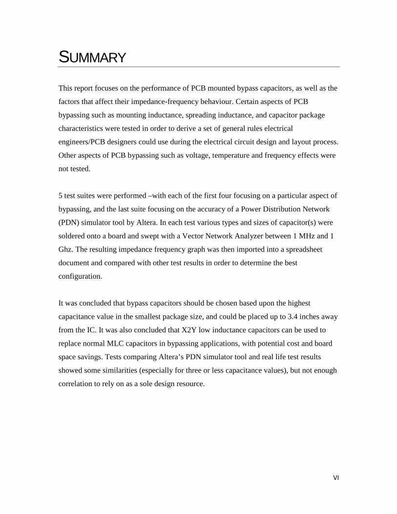
SUMMARY This report focuses on the performance of PCB mounted bypass capacitors, as well as the
factors that affect their impedance-frequency behaviour. Certain aspects of PCB
bypassing such as mounting inductance, spreading inductance, and capacitor package
characteristics were tested in order to derive a set of general rules electrical
engineers/PCB designers could use during the electrical circuit design and layout process.
Other aspects of PCB bypassing such as voltage, temperature and frequency effects were
not tested.
5 test suites were performed –with each of the first four focusing on a particular aspect of
bypassing, and the last suite focusing on the accuracy of a Power Distribution Network
(PDN) simulator tool by Altera. In each test various types and sizes of capacitor(s) were
soldered onto a board and swept with a Vector Network Analyzer between 1 MHz and 1
Ghz. The resulting impedance frequency graph was then imported into a spreadsheet
document and compared with other test results in order to determine the best
configuration.
It was concluded that bypass capacitors should be chosen based upon the highest
capacitance value in the smallest package size, and could be placed up to 3.4 inches away
from the IC. It was also concluded that X2Y low inductance capacitors can be used to
replace normal MLC capacitors in bypassing applications, with potential cost and board
space savings. Tests comparing Altera’s PDN simulator tool and real life test results
showed some similarities (especially for three or less capacitance values), but not enough
correlation to rely on as a sole design resource.
Christie Digital Systems | Introduction 1
1. INTRODUCTION Supplying a constant stable voltage to power IC’s with high clock frequencies
such as FPGA’s require careful Power Distribution Network (PDN) design in
order to prevent unstable operation or component failure. A major component of
PDN design is effective bypass capacitor selection and placement on PCB’s.
There are multiple factors that affect the performance of these bypass capacitors,
but they can be separated into two general categories: capacitor selection and
design, and PCB design. Capacitor selection and design refers to certain
characteristics such as capacitance, structure and size, and bypass rules of thumb.
PCB design refers to characteristics such as distance away from IC, board
stackup, and via number. This report shows the results of testing each of these
factors, as well as any conclusions and recommendations drawn from these
results.
For a more in depth explanation, please refer to Appendix A: Background on PCB
Bypassing.
1.1. GENERAL OBJECTIVE The objective of this report is to draw practical methods of improving bypassing
of high frequency power networks through the testing of capacitor selection and
placement on PCB’s. The recommendations from this report will reduce the
overall cost and time engineers need to spend on PDN design, and represent a
source of substantial resource savings for the company.
Christie Digital Systems | Technical Objectives 2
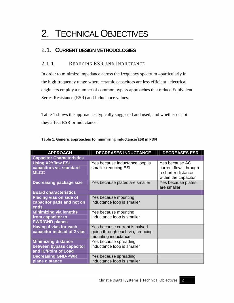
2. TECHNICAL OBJECTIVES 2.1. CURRENT DESIGN METHODOLOGIES
2.1.1. REDUCING ESR AND INDUCTANCE
In order to minimize impedance across the frequency spectrum –particularly in
the high frequency range where ceramic capacitors are less efficient– electrical
engineers employ a number of common bypass approaches that reduce Equivalent
Series Resistance (ESR) and Inductance values.
Table 1 shows the approaches typically suggested and used, and whether or not
they affect ESR or inductance:
Table 1: Generic approaches to minimizing inductance/ESR in PDN
APPROACH DECREASES INDUCTANCE DECREASES ESR Capacitor Characteristics Using X2Y/low ESL capacitors vs. standard MLCC
Yes because inductance loop is smaller reducing ESL
Yes because AC current flows through a shorter distance within the capacitor
Decreasing package size Yes because plates are smaller Yes because plates are smaller
Board characteristics Placing vias on side of capacitor pads and not on ends
Yes because mounting inductance loop is smaller
Minimizing via lengths from capacitor to PWR/GND planes
Yes because mounting inductance loop is smaller
Having 4 vias for each capacitor instead of 2 vias
Yes because current is halved going through each via, reducing mounting inductance
Minimizing distance between bypass capacitor and IC/Point of Load
Yes because spreading inductance loop is smaller
Decreasing GND-PWR plane distance
Yes because spreading inductance loop is smaller
Christie Digital Systems | Technical Objectives 3
2.1.2. COMMON BYPASS RULES OF THUMB
Because of the complex interactions when dealing with multiple capacitors,
electrical engineers often employ rules of thumb when selecting bypass capacitor
values and sizes. Three rules of thumb are commonly seen in circuit schematics
and used by PCB designers: Decades Rule, Highest Value Smallest Package, and
Capacitance Mix.
1. Decades rule: bypass capacitors have capacitances in multiples of 10 -
such as 10nF, 100nF, and 1μF. 100nF and 1μF are commonly seen in
circuit schematics.
2. Highest Value Smallest Package: bypass capacitors have the largest
possible capacitance value while using the smallest possible package size
aspect ratio. For example if using 0402 and 0201 package sizes, the only
capacitance values used are 10μF and 1μF respectively (the largest
possible capacitance that can be manufactured for each aspect ratio).
3. Capacitance Mix: Using a PDN simulator such as Altera’s “PDN tool”, a
broad range of capacitor aspect ratios and capacitances are selected in
order to reduce impedance below a set “Target Impedance”.
2.2. PROBLEMS WITH CURRENT DESIGN METHODOLOGIES The current design methodologies –although widely in use– have a number of
issues associated:
1. AC frequencies up to 1MHz are well filtered using electrolytic bulk
capacitors and large value ceramic bypass capacitors, but higher
frequencies in the tens and hundreds of megahertz are much more
difficult to filter due to interference with plane capacitance and sensitivity
to parasitic inductance.
2. Table 1 illustrates a number of generic approaches an engineer can follow
to ensure minimal impedance across the frequency spectrum, but there
Christie Digital Systems | Technical Objectives 4
have been no tests conducted in which each of the approaches is
compared and measured to see just how effective they are. For example
Table 1 advises that placing bypass capacitors as close as possible to the
IC’s power pin minimizes the spreading inductance. However the
question of “how close is close enough” often arises, and placing the
capacitor a few millimetres farther away from the IC may cause the
impedance to only rise by a few milliohms while allowing for a more
efficient board design overall.
3. Table 1 also does not specify what particular capacitance values should
be chosen when bypassing, since this can vary depending on the clock
frequency of the IC, the environment the PCB is operating in, as well as
the board layout and design.
4. Choosing the right bypass capacitor values and size is often an educated
guess, with engineers picking one bypass rule of thumb or another (or
none) with minimal test results to back up their choice. Furthermore any
mistakes related to capacitor selection and placement is difficult and
costly to fix since a large amount of money and time had been spent
developing the initial PCB.
Because of the difficulty of accounting for all these factors, engineers often rely
on simulations that oversimplify the system, or default to one of the rules of
thumb.
Christie Digital Systems | Technical Objectives 5
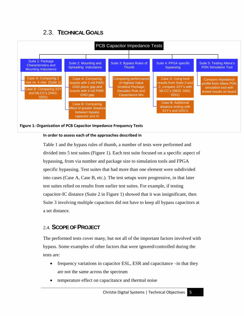
2.3. TECHNICAL GOALS
PCB Capacitor Impedance Tests
Suite 2: Mounting and Spreading Inductance
Suite 4: FPGA specific bypassing
Suite 5: Testing Altera’s PDN Simulation Tool
Suite 3: Bypass Rules of Thumb
Case A: Comparing 2 vias vs. 4 vias (Suite 1)
Case A: Comparing boards with 2 mil PWR-
GND plane gap and boards with 4 mil PWR-
GND gap
Case B: Comparing effect of greater distance
between bypass capacitor and IC
Comparing performance of Highest Value
Smallest Package, Decades Rule and Capacitance Mix
Compare impedance profile from Altera PDN
simulation tool with tested results on board
Case A: Using best results from Suite 3 and 2, compare X2Y’s with MLCC’s (0603, 0402,
0201)
Case B: Additional distance testing with
X2Y’s and 0201's
Suite 1: Package Characteristics and
Mounting Inductance
Case B: Comparing X2Y and MLCC’s (0402,
0201)
Figure 1: Organization of PCB Capacitor Impedance Frequency Tests
In order to assess each of the approaches described in
Table 1 and the bypass rules of thumb, a number of tests were performed and
divided into 5 test suites (Figure 1). Each test suite focused on a specific aspect of
bypassing, from via number and package size to simulation tools and FPGA
specific bypassing. Test suites that had more than one element were subdivided
into cases (Case A, Case B, etc.). The test setups were progressive, in that later
test suites relied on results from earlier test suites. For example, if testing
capacitor-IC distance (Suite 2 in Figure 1) showed that it was insignificant, then
Suite 3 involving multiple capacitors did not have to keep all bypass capacitors at
a set distance.
2.4. SCOPE OF PROJECT
The performed tests cover many, but not all of the important factors involved with
bypass. Some examples of other factors that were ignored/controlled during the
tests are:
• frequency variations in capacitor ESL, ESR and capacitance –in that they
are not the same across the spectrum
• temperature effect on capacitance and thermal noise
Christie Digital Systems | Technical Objectives 6
• Different ESL/ESR depending on ceramic dielectric in the capacitor
• Different capacitance depending on the voltage level being decoupled
However the general scope of the tests was on elements that the designer can
control easily and cost-effectively, such as capacitance, aspect ratio/size,
placement and board design. Temperature, frequency and voltage effects on
bypass capacitors are inevitable and cannot be efficiently controlled enough to
warrant specific testing. Dielectric cannot be specified and is determined by the
capacitor manufacturer.
Christie Digital Systems | General Setup and Procedure 7
3. GENERAL SETUP AND PROCEDURE 3.1. TEST EQUIPMENT
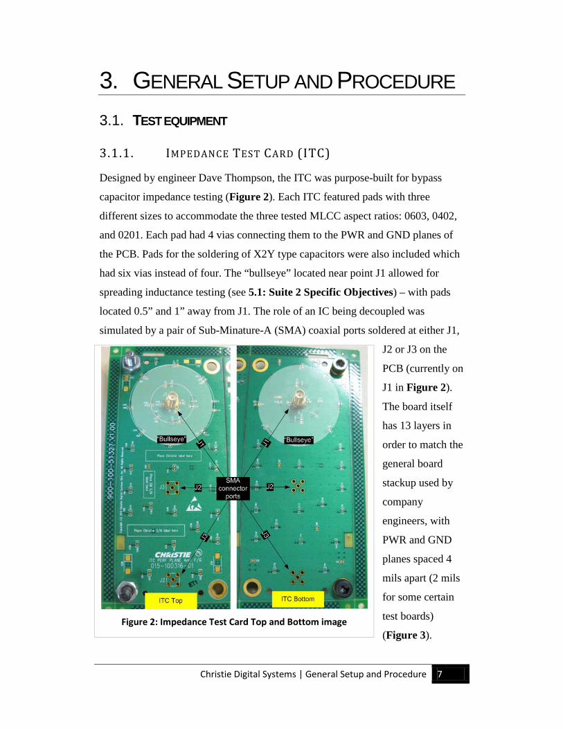
3.1.1. IMPEDANCE TEST CARD (ITC)
Designed by engineer Dave Thompson, the ITC was purpose-built for bypass
capacitor impedance testing (Figure 2). Each ITC featured pads with three
different sizes to accommodate the three tested MLCC aspect ratios: 0603, 0402,
and 0201. Each pad had 4 vias connecting them to the PWR and GND planes of
the PCB. Pads for the soldering of X2Y type capacitors were also included which
had six vias instead of four. The “bullseye” located near point J1 allowed for
spreading inductance testing (see 5.1: Suite 2 Specific Objectives) – with pads
located 0.5” and 1” away from J1. The role of an IC being decoupled was
simulated by a pair of Sub-Minature-A (SMA) coaxial ports soldered at either J1,
J2 or J3 on the
PCB (currently on
J1 in Figure 2).
The board itself
has 13 layers in
order to match the
general board
stackup used by
company
engineers, with
PWR and GND
planes spaced 4
mils apart (2 mils
for some certain
test boards)
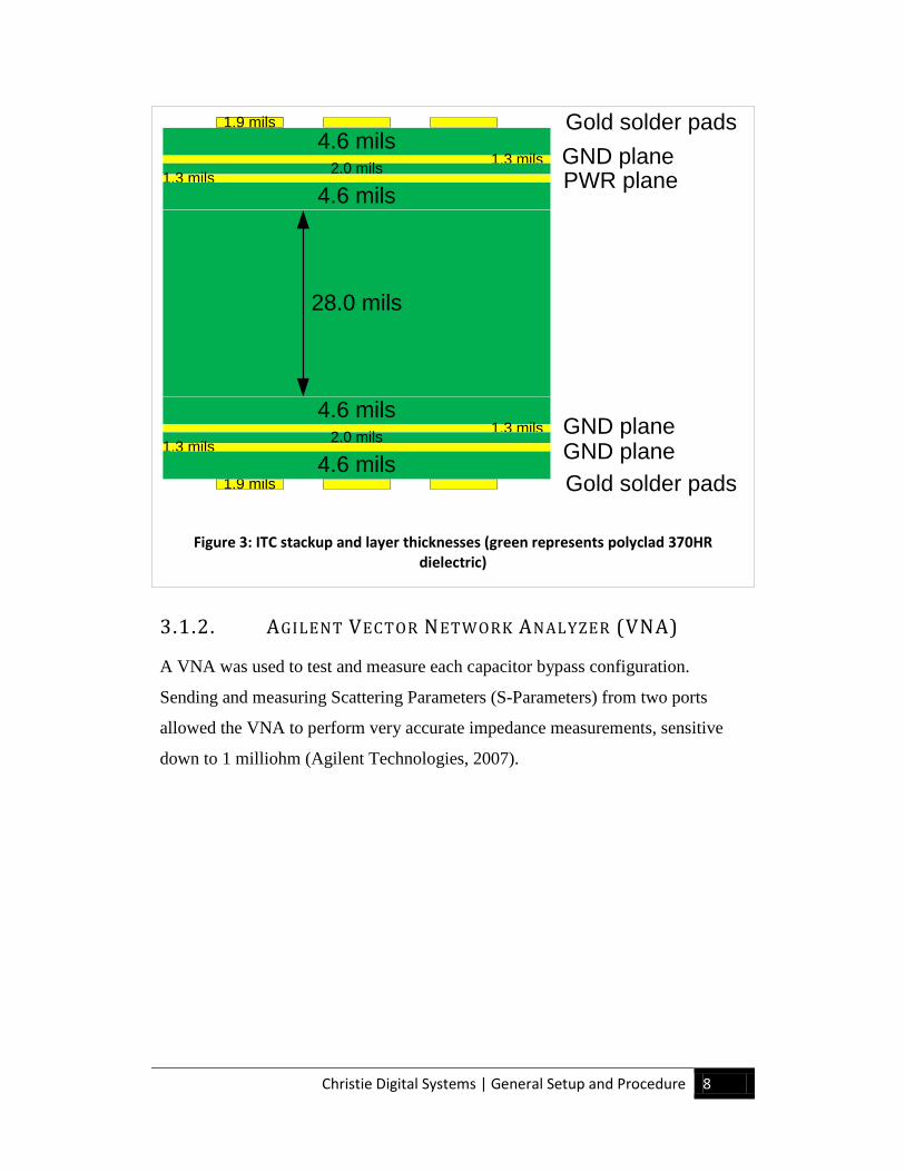
(Figure 3).
Figure 2: Impedance Test Card Top and Bottom image
Christie Digital Systems | General Setup and Procedure 8
1.9 mils4.6 mils
1.3 mils2.0 mils1.3 mils4.6 mils
28.0 mils
1.9 mils
4.6 mils1.3 mils2.0 mils1.3 mils
4.6 mils
Gold solder pads
Gold solder pads
PWR planeGND plane
GND planeGND plane
Figure 3: ITC stackup and layer thicknesses (green represents polyclad 370HR dielectric)
3.1.2. AGILENT VECTOR NETWORK ANALYZER (VNA)
A VNA was used to test and measure each capacitor bypass configuration.
Sending and measuring Scattering Parameters (S-Parameters) from two ports
allowed the VNA to perform very accurate impedance measurements, sensitive
down to 1 milliohm (Agilent Technologies, 2007).
Christie Digital Systems | General Setup and Procedure 9
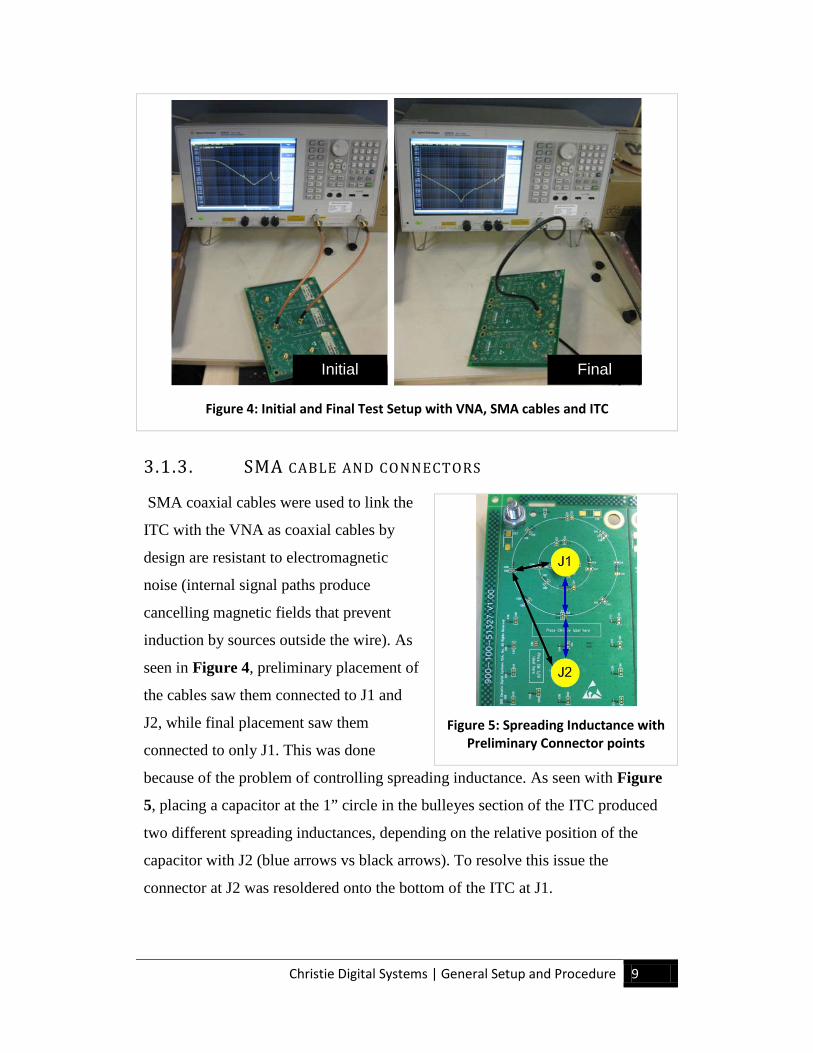
3.1.3. SMA CABLE AND CONNECTORS
SMA coaxial cables were used to link the
ITC with the VNA as coaxial cables by
design are resistant to electromagnetic
noise (internal signal paths produce
cancelling magnetic fields that prevent
induction by sources outside the wire). As
seen in Figure 4, preliminary placement of
the cables saw them connected to J1 and
J2, while final placement saw them
connected to only J1. This was done
because of the problem of controlling spreading inductance. As seen with Figure
5, placing a capacitor at the 1” circle in the bulleyes section of the ITC produced
two different spreading inductances, depending on the relative position of the
capacitor with J2 (blue arrows vs black arrows). To resolve this issue the
connector at J2 was resoldered onto the bottom of the ITC at J1.
Initial Final
Figure 4: Initial and Final Test Setup with VNA, SMA cables and ITC
Figure 5: Spreading Inductance with
Preliminary Connector points
Christie Digital Systems | General Setup and Procedure 10
3.2. TEST PROCEDURE
3.2.1. CALIBRATION AND CONTROLLED PARAMETERS
In order to account for signal losses and reflections between the Impedance
Analyzer (VNA) and the Impedance Test Card (ITC), calibration of the setup had
to be performed. Specifically three calibrations needed to be done before each
test: an Open Short Load Calibration, a Thru Calibration and a Port Extensions
Calibration.
• Open Short Load Calibration: Conducted before hooking up the SMA
cables to the PCB, using three standards –an open circuit, a short circuit
and an exact resistive load- that attached to the end of each SMA cable.
This calibration minimized the measurement error due to EMI
• Thru Calibration: Conducted by linking cables from both VNA S-
paramater ports together. This calibration minimized the error due to
signal attenuation/ loss within the SMA cables.
• Port Extensions Calibration: Conducted by attaching the SMA cables to
a non-populated (ie. no solderd capacitors) PCB. This calibration
minimized the error due to differences in characteristic impedance
between SMA cables and the PCB PWR and GND planes. Not accounting
for this would have led to false results due to signal reflection
Each test suite had certain controlled parameters (such as capacitance, aspect ratio
of capacitor, etc.) in order to ensure only one factor was being tested at a time.
3.2.2. GENERAL TEST PROCEDURE
Calibration of the VNA, SMA cables and PCB was performed using the
procedures described in 3.2.1: Calibration and Controlled Parameters. The 4
mil PCB was then removed from the SMA cables and the capacitors were
soldered into position on the board by hand. Once the capacitor(s) were soldered,
the board was reattached to the VNA and was tested between 1MHz and 1GHz.
This data was then exported to an excel spreadsheet for further analysis.
Christie Digital Systems | Test Suite 1 11
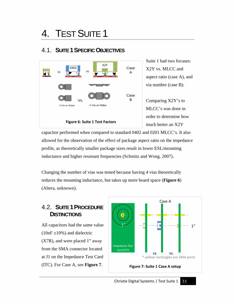
4. TEST SUITE 1 4.1. SUITE 1 SPECIFIC OBJECTIVES
Suite 1 had two focuses:
X2Y vs. MLCC and
aspect ratio (case A), and
via number (case B).
Comparing X2Y’s to
MLCC’s was done in
order to determine how
much better an X2Y
capacitor performed when compared to standard 0402 and 0201 MLCC’s. It also
allowed for the observation of the effect of package aspect ratio on the impedance
profile, as theoretically smaller package sizes result in lower ESL/mounting
inductance and higher resonant frequencies (Schmitz and Wong, 2007).
Changing the number of vias was tested because having 4 vias theoretically
reduces the mounting inductance, but takes up more board space (Figure 6)
(Altera, unknown).
4.2. SUITE 1 PROCEDURE DISTINCTIONS
All capacitors had the same value
(10nF ±10%) and dielectric
(X7R), and were placed 1” away
from the SMA connector located
at J1 on the Impedance Test Card
(ITC). For Case A, see Figure 7.
vs
X2Y 0402
0201 vs
Vs.
Case A
Case B
Figure 6: Suite 1 Test Factors
1”
vs. * yellow rectangles are SMA ports
1”
Impedance Test Card (ITC)
J1
vs.
Case A
Figure 7: Suite 1 Case A setup
Christie Digital Systems | Test Suite 1 12
For Case B, up to four 0201 sized capacitors were tested with the VNA, first with
4 vias going to each capacitor, and then 2 vias. The decrease in vias was
accomplished by physically cutting the surface traces connecting the capacitor
pads to the vias.
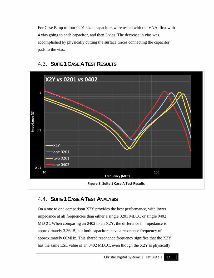
4.3. SUITE 1 CASE A TEST RESULTS
Figure 8: Suite 1 Case A Test Results
4.4. SUITE 1 CASE A TEST ANALYSIS On a one to one comparison X2Y provides the best performance, with lower
impedance at all frequencies than either a single 0201 MLCC or single 0402
MLCC. When comparing an 0402 to an X2Y, the difference in impedance is
approximately 3.36dB, but both capacitors have a resonance frequency of
approximately 60MHz. This shared resonance frequency signifies that the X2Y
has the same ESL value of an 0402 MLCC, even though the X2Y is physically
0.01
0.1
1
10 100
Impe
danc
e (Ω
)
Frequency (MHz)
X2Y vs 0201 vs 0402
X2Y one 0201 two 0201 one 0402
Christie Digital Systems | Test Suite 1 13
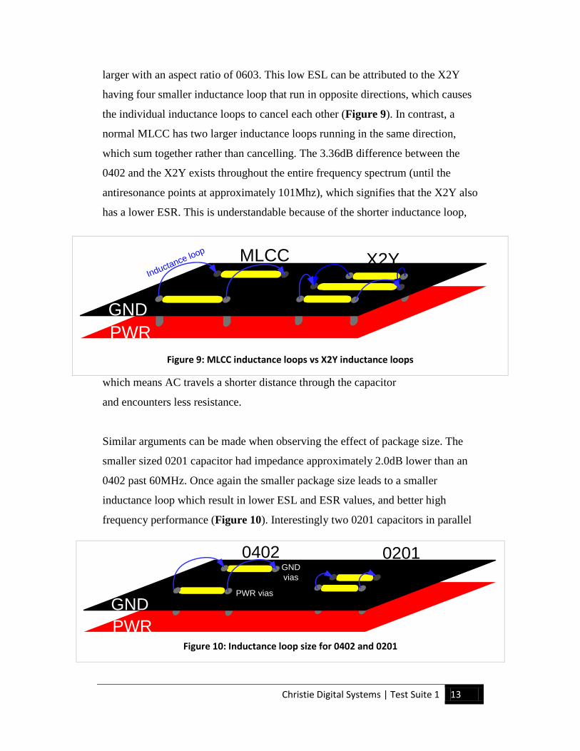
larger with an aspect ratio of 0603. This low ESL can be attributed to the X2Y
having four smaller inductance loop that run in opposite directions, which causes
the individual inductance loops to cancel each other (Figure 9). In contrast, a
normal MLCC has two larger inductance loops running in the same direction,
which sum together rather than cancelling. The 3.36dB difference between the
0402 and the X2Y exists throughout the entire frequency spectrum (until the
antiresonance points at approximately 101Mhz), which signifies that the X2Y also
has a lower ESR. This is understandable because of the shorter inductance loop,
which means AC travels a shorter distance through the capacitor
and encounters less resistance.
Similar arguments can be made when observing the effect of package size. The
smaller sized 0201 capacitor had impedance approximately 2.0dB lower than an
0402 past 60MHz. Once again the smaller package size leads to a smaller
inductance loop which result in lower ESL and ESR values, and better high
frequency performance (Figure 10). Interestingly two 0201 capacitors in parallel
GNDPWR
Inductance loop MLCC X2Y
Figure 9: MLCC inductance loops vs X2Y inductance loops
GNDPWR
PWR vias
0402GND vias
0201
Figure 10: Inductance loop size for 0402 and 0201
Christie Digital Systems | Test Suite 1 14
perform almost at the same level as an X2Y, but their total ESL is still greater
than a single X2Y.
4.5. SUITE 1 CASE B TEST RESULTS
Figure 11: Suite 1 Case B Test Result
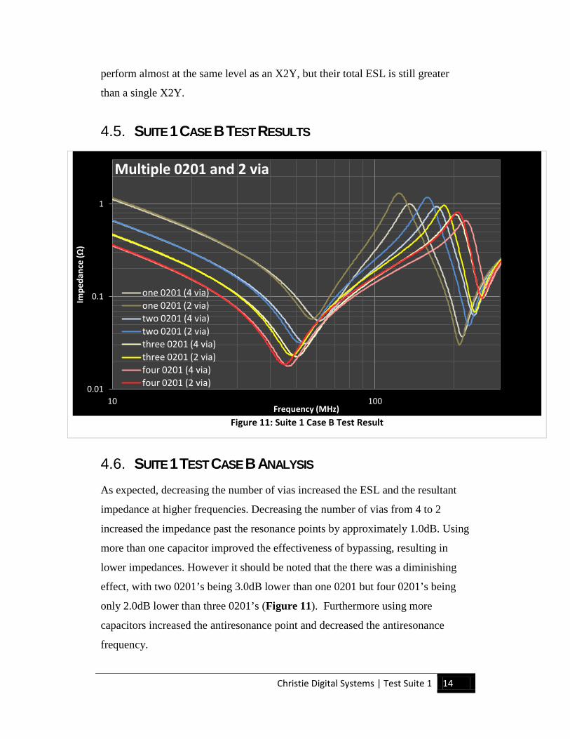
4.6. SUITE 1 TEST CASE B ANALYSIS As expected, decreasing the number of vias increased the ESL and the resultant
impedance at higher frequencies. Decreasing the number of vias from 4 to 2
increased the impedance past the resonance points by approximately 1.0dB. Using
more than one capacitor improved the effectiveness of bypassing, resulting in
lower impedances. However it should be noted that the there was a diminishing
effect, with two 0201’s being 3.0dB lower than one 0201 but four 0201’s being
only 2.0dB lower than three 0201’s (Figure 11). Furthermore using more
capacitors increased the antiresonance point and decreased the antiresonance
frequency.
0.01
0.1
1
10 100
Impe
danc
e (Ω
)
Frequency (MHz)
Multiple 0201 and 2 via
one 0201 (4 via) one 0201 (2 via) two 0201 (4 via) two 0201 (2 via) three 0201 (4 via) three 0201 (2 via) four 0201 (4 via) four 0201 (2 via)
Christie Digital Systems | Test Suite 2 15
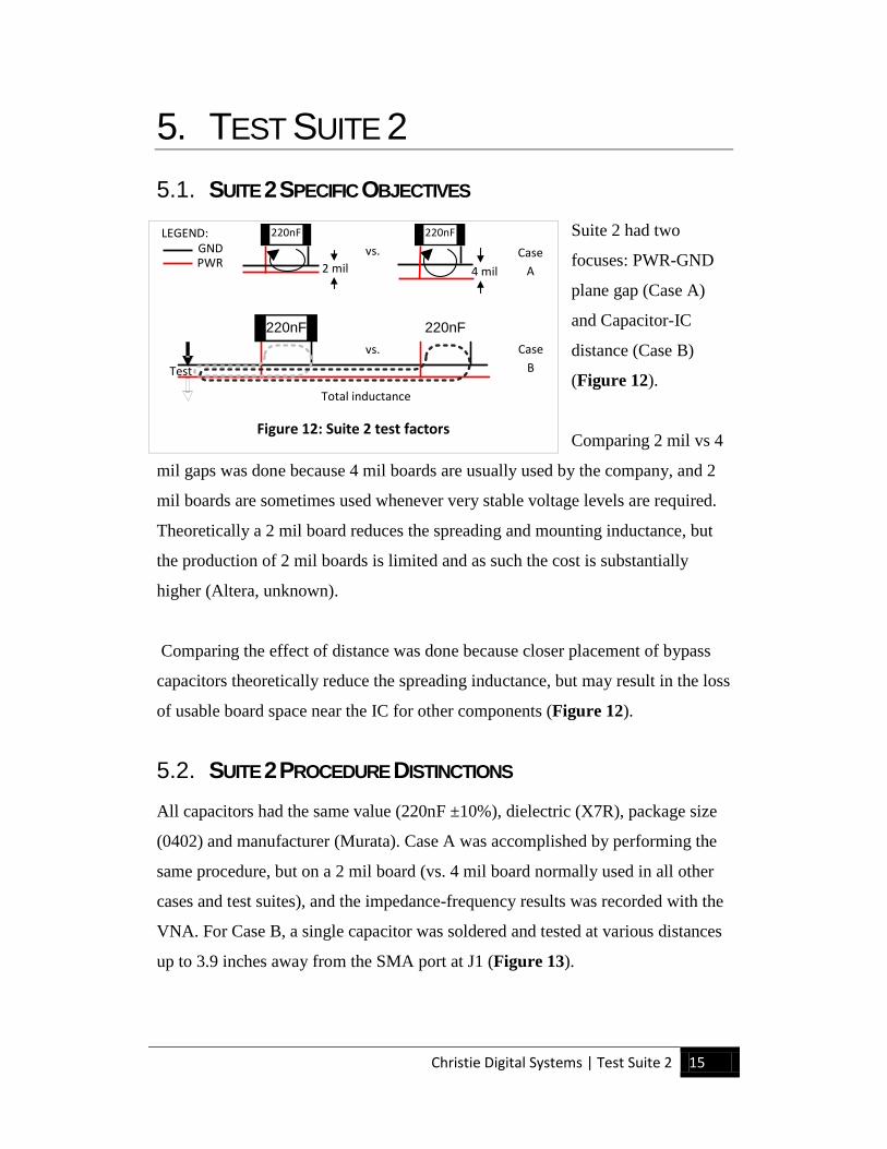
5. TEST SUITE 2 5.1. SUITE 2 SPECIFIC OBJECTIVES
Suite 2 had two
focuses: PWR-GND
plane gap (Case A)
and Capacitor-IC
distance (Case B)
(Figure 12).
Comparing 2 mil vs 4
mil gaps was done because 4 mil boards are usually used by the company, and 2
mil boards are sometimes used whenever very stable voltage levels are required.
Theoretically a 2 mil board reduces the spreading and mounting inductance, but
the production of 2 mil boards is limited and as such the cost is substantially
higher (Altera, unknown).
Comparing the effect of distance was done because closer placement of bypass
capacitors theoretically reduce the spreading inductance, but may result in the loss
of usable board space near the IC for other components (Figure 12).
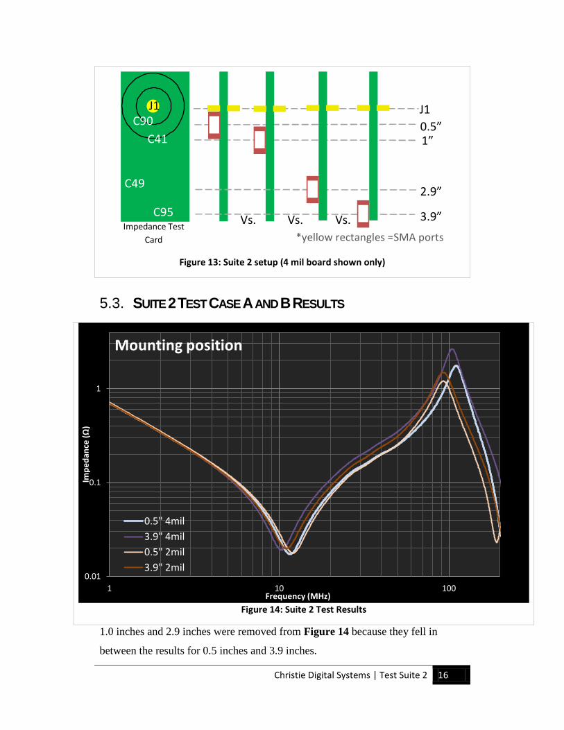
5.2. SUITE 2 PROCEDURE DISTINCTIONS All capacitors had the same value (220nF ±10%), dielectric (X7R), package size
(0402) and manufacturer (Murata). Case A was accomplished by performing the
same procedure, but on a 2 mil board (vs. 4 mil board normally used in all other
cases and test suites), and the impedance-frequency results was recorded with the
VNA. For Case B, a single capacitor was soldered and tested at various distances
up to 3.9 inches away from the SMA port at J1 (Figure 13).
220nF 220nF
Test
GND PWR
LEGEND: vs.
220nF
2 mil 4 mil
220nF
vs.
Case A
Case B
Total inductance Figure 12: Suite 2 test factors
Christie Digital Systems | Test Suite 2 16
J1 0.5”
*yellow rectangles =SMA ports
1”
2.9”
3.9” Vs. Vs. Vs.
C90
Impedance Test Card
C41
J1
C49
C95
Figure 13: Suite 2 setup (4 mil board shown only)
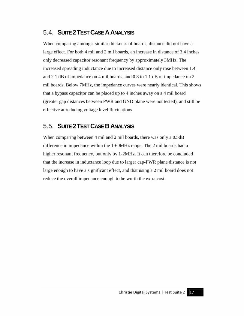
5.3. SUITE 2 TEST CASE A AND B RESULTS
Figure 14: Suite 2 Test Results
1.0 inches and 2.9 inches were removed from Figure 14 because they fell in
between the results for 0.5 inches and 3.9 inches.
0.01
0.1
1
1 10 100
Impe
danc
e (Ω
)
Frequency (MHz)
Mounting position
0.5" 4mil 3.9" 4mil 0.5" 2mil 3.9" 2mil
0.01
0.1
1
1 10 100
Impe
danc
e (Ω
)
Frequency (MHz)
Mounting position
0.5" 4mil
3.9" 4mil
0.5" 2mil
3.9" 2mil
Christie Digital Systems | Test Suite 2 17
5.4. SUITE 2 TEST CASE A ANALYSIS When comparing amongst similar thickness of boards, distance did not have a
large effect. For both 4 mil and 2 mil boards, an increase in distance of 3.4 inches
only decreased capacitor resonant frequency by approximately 3MHz. The
increased spreading inductance due to increased distance only rose between 1.4
and 2.1 dB of impedance on 4 mil boards, and 0.8 to 1.1 dB of impedance on 2
mil boards. Below 7MHz, the impedance curves were nearly identical. This shows
that a bypass capacitor can be placed up to 4 inches away on a 4 mil board
(greater gap distances between PWR and GND plane were not tested), and still be
effective at reducing voltage level fluctuations.
5.5. SUITE 2 TEST CASE B ANALYSIS When comparing between 4 mil and 2 mil boards, there was only a 0.5dB
difference in impedance within the 1-60MHz range. The 2 mil boards had a
higher resonant frequency, but only by 1-2MHz. It can therefore be concluded
that the increase in inductance loop due to larger cap-PWR plane distance is not
large enough to have a significant effect, and that using a 2 mil board does not
reduce the overall impedance enough to be worth the extra cost.
Christie Digital Systems | Test Suite 3 18
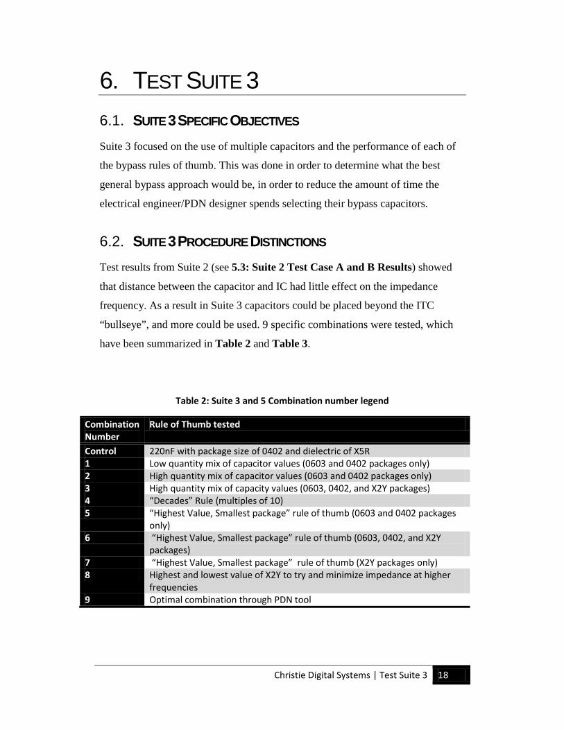
6. TEST SUITE 3 6.1. SUITE 3 SPECIFIC OBJECTIVES Suite 3 focused on the use of multiple capacitors and the performance of each of
the bypass rules of thumb. This was done in order to determine what the best
general bypass approach would be, in order to reduce the amount of time the
electrical engineer/PDN designer spends selecting their bypass capacitors.
6.2. SUITE 3 PROCEDURE DISTINCTIONS Test results from Suite 2 (see 5.3: Suite 2 Test Case A and B Results) showed
that distance between the capacitor and IC had little effect on the impedance
frequency. As a result in Suite 3 capacitors could be placed beyond the ITC
“bullseye”, and more could be used. 9 specific combinations were tested, which
have been summarized in Table 2 and Table 3.
Table 2: Suite 3 and 5 Combination number legend
Combination Number
Rule of Thumb tested
Control 220nF with package size of 0402 and dielectric of X5R 1 Low quantity mix of capacitor values (0603 and 0402 packages only) 2 High quantity mix of capacitor values (0603 and 0402 packages only) 3 High quantity mix of capacity values (0603, 0402, and X2Y packages) 4 “Decades” Rule (multiples of 10) 5 “Highest Value, Smallest package” rule of thumb (0603 and 0402 packages
only) 6 “Highest Value, Smallest package” rule of thumb (0603, 0402, and X2Y
packages) 7 “Highest Value, Smallest package” rule of thumb (X2Y packages only) 8 Highest and lowest value of X2Y to try and minimize impedance at higher
frequencies 9 Optimal combination through PDN tool
Christie Digital Systems | Test Suite 3 19
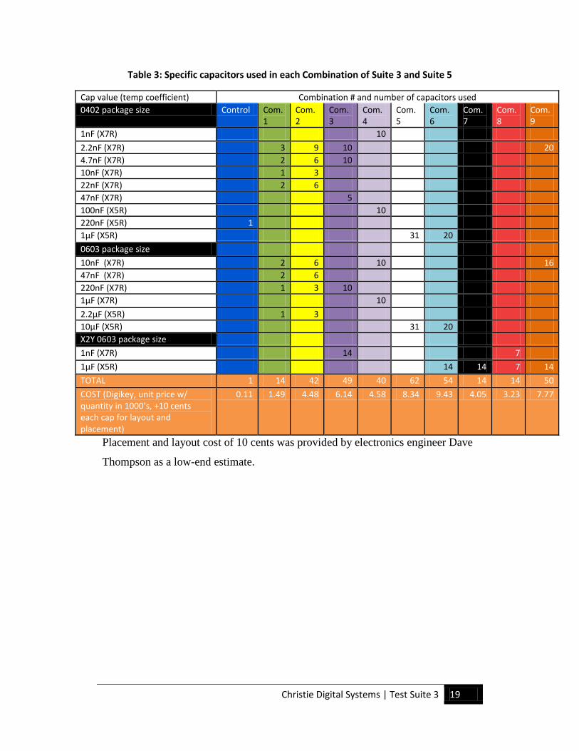
Table 3: Specific capacitors used in each Combination of Suite 3 and Suite 5
Cap value (temp coefficient) Combination # and number of capacitors used 0402 package size Control Com.
1 Com. 2
Com. 3
Com.4
Com. 5
Com. 6
Com. 7
Com. 8
Com. 9
1nF (X7R) 10 2.2nF (X7R) 3 9 10 20 4.7nF (X7R) 2 6 10 10nF (X7R) 1 3 22nF (X7R) 2 6 47nF (X7R) 5 100nF (X5R) 10 220nF (X5R) 1 1µF (X5R) 31 20 0603 package size 10nF (X7R) 2 6 10 16 47nF (X7R) 2 6 220nF (X7R) 1 3 10 1µF (X7R) 10 2.2µF (X5R) 1 3 10µF (X5R) 31 20 X2Y 0603 package size 1nF (X7R) 14 7 1µF (X5R) 14 14 7 14 TOTAL 1 14 42 49 40 62 54 14 14 50 COST (Digikey, unit price w/ quantity in 1000’s, +10 cents each cap for layout and placement)
0.11 1.49 4.48 6.14 4.58 8.34 9.43 4.05 3.23 7.77
Placement and layout cost of 10 cents was provided by electronics engineer Dave
Thompson as a low-end estimate.
Christie Digital Systems | Test Suite 3 20
6.3. SUITE 3 RESULTS
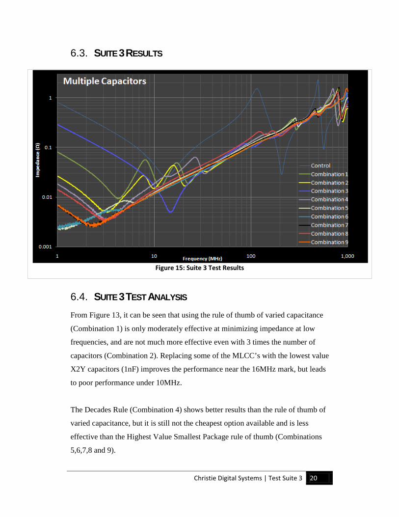
6.4. SUITE 3 TEST ANALYSIS From Figure 13, it can be seen that using the rule of thumb of varied capacitance
(Combination 1) is only moderately effective at minimizing impedance at low
frequencies, and are not much more effective even with 3 times the number of
capacitors (Combination 2). Replacing some of the MLCC’s with the lowest value
X2Y capacitors (1nF) improves the performance near the 16MHz mark, but leads
to poor performance under 10MHz.
The Decades Rule (Combination 4) shows better results than the rule of thumb of
varied capacitance, but it is still not the cheapest option available and is less
effective than the Highest Value Smallest Package rule of thumb (Combinations
5,6,7,8 and 9).
Figure 15: Suite 3 Test Results
Christie Digital Systems | Test Suite 3 21
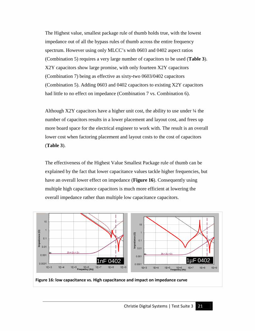
The Highest value, smallest package rule of thumb holds true, with the lowest
impedance out of all the bypass rules of thumb across the entire frequency
spectrum. However using only MLCC’s with 0603 and 0402 aspect ratios
(Combination 5) requires a very large number of capacitors to be used (Table 3).
X2Y capacitors show large promise, with only fourteen X2Y capacitors
(Combination 7) being as effective as sixty-two 0603/0402 capacitors
(Combination 5). Adding 0603 and 0402 capacitors to existing X2Y capacitors
had little to no effect on impedance (Combination 7 vs. Combination 6).
Although X2Y capacitors have a higher unit cost, the ability to use under ¼ the
number of capacitors results in a lower placement and layout cost, and frees up
more board space for the electrical engineer to work with. The result is an overall
lower cost when factoring placement and layout costs to the cost of capacitors
(Table 3).
The effectiveness of the Highest Value Smallest Package rule of thumb can be
explained by the fact that lower capacitance values tackle higher frequencies, but
have an overall lower effect on impedance (Figure 16). Consequently using
multiple high capacitance capacitors is much more efficient at lowering the
overall impedance rather than multiple low capacitance capacitors.
1nF 0402 1µF 0402
Figure 16: low capacitance vs. High capacitance and impact on impedance curve

Christie Digital Systems | Test Suite 3 22
Interestingly, all combinations except control exhibited a similar effect on
impedance above 30MHz no matter what combination was tried. This can be
explained by Figure 16 in that the 1μF capacitor had a lower resonant frequency,
but the impedance at that resonant point was significantly lower than the 1nF
capacitor. As the capacitance decreases, the resonant frequency increases but the
impedance at that resonance point increases.
Christie Digital Systems | Test Suite 4 23
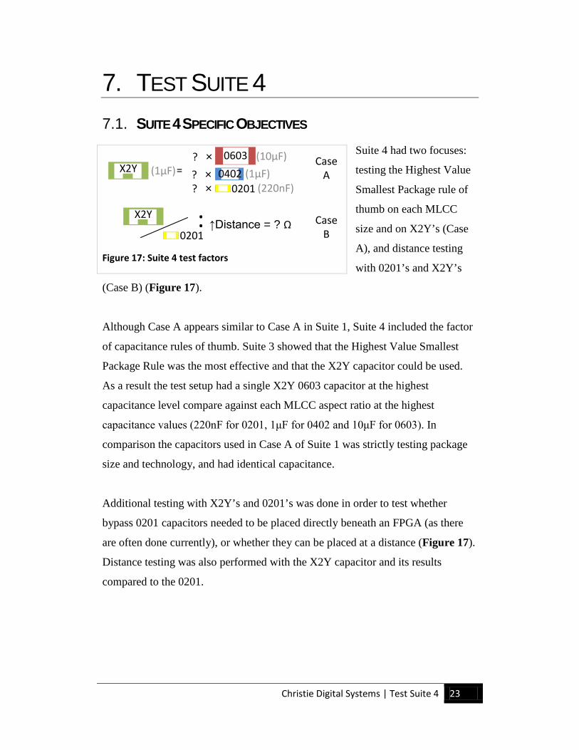
7. TEST SUITE 4 7.1. SUITE 4 SPECIFIC OBJECTIVES
Suite 4 had two focuses:
testing the Highest Value
Smallest Package rule of
thumb on each MLCC
size and on X2Y’s (Case
A), and distance testing
with 0201’s and X2Y’s
(Case B) (Figure 17).
Although Case A appears similar to Case A in Suite 1, Suite 4 included the factor
of capacitance rules of thumb. Suite 3 showed that the Highest Value Smallest
Package Rule was the most effective and that the X2Y capacitor could be used.
As a result the test setup had a single X2Y 0603 capacitor at the highest
capacitance level compare against each MLCC aspect ratio at the highest
capacitance values (220nF for 0201, 1μF for 0402 and 10μF for 0603). In
comparison the capacitors used in Case A of Suite 1 was strictly testing package
size and technology, and had identical capacitance.
Additional testing with X2Y’s and 0201’s was done in order to test whether
bypass 0201 capacitors needed to be placed directly beneath an FPGA (as there
are often done currently), or whether they can be placed at a distance (Figure 17).
Distance testing was also performed with the X2Y capacitor and its results
compared to the 0201.
X2Y =? ×? ×
0603
0402 0201? ×
X2Y
0201: ↑Distance = ? Ω
Case A
Case B
(1μF) (1μF)(10μF)
(220nF)
Figure 17: Suite 4 test factors
Christie Digital Systems | Test Suite 4 24
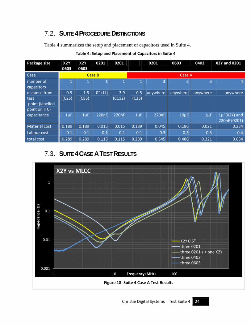
7.2. SUITE 4 PROCEDURE DISTINCTIONS Table 4 summarizes the setup and placement of capacitors used in Suite 4.
Table 4: Setup and Placement of Capacitors in Suite 4
Package size X2Y 0603
X2Y 0603
0201 0201 0201 0603 0402 X2Y and 0201
Case Case B Case A number of capacitors
1 1 1 1 1 3 3 3 4
distance from test point (labelled point on ITC)
0.5 (C25)
1.5 (C85)
0” (J1) 3.9 (C112)
0.5 (C25)
anywhere anywhere anywhere anywhere
capacitance 1µF 1µF 220nF 220nF 1μF 220nF 10µF 1µF 1µF(X2Y) and 220nF (0201)
Material cost 0.189 0.189 0.015 0.015 0.189 0.045 0.186 0.021 0.234 Labour cost 0.1 0.1 0.1 0.1 0.1 0.3 0.3 0.3 0.4 total cost 0.289 0.289 0.115 0.115 0.289 0.345 0.486 0.321 0.634
7.3. SUITE 4 CASE A TEST RESULTS
Figure 18: Suite 4 Case A Test Results
0.001
0.01
0.1
1
1 10 100
Impe
danc
e (Ω
)
Frequency (MHz)
X2Y vs MLCC
X2Y 0.5" three 0201 three 0201's + one X2Y three 0402 three 0603

Christie Digital Systems | Test Suite 4 25
7.4. SUITE 4 CASE A ANALYSIS From Figure 18, three 0201’s at 220nF each produced comparable impedance
curve to a single X2Y with a capacitance of 1μF at 0.5 inches, but with a resonant
frequency 3.6MHz higher. Three 0402’s at 1μF and three 0603’s at 10μF
produced lower resonant impedances than a single X2Y (0.005Ω for 0402 and
0.004Ω for 0603 vs. 0.01Ω for X2Y), but at lower frequencies. Combining three
0201’s at 220nF with an X2Y at 1μF produced an overall 1.7dB drop in
impedance across all frequencies when compared to single 1μF X2Y at 0.5
inches. These results show that an X2Y capacitor following the highest value
smallest package rule is an effective replacement for three 0402 MLCC’s
following the same bypass rule of thumb. The X2Y is slightly more expensive -
but this cost difference is offset with the savings in board space, giving the board
designer more room to layout crucial components and signal traces without
conflicting with a bypass capacitor. Alternatively Figure 18 shows that three
0201 MLCC’s at their highest value (220nF) could be used in place of the X2Y
capacitor.
Christie Digital Systems | Test Suite 4 26
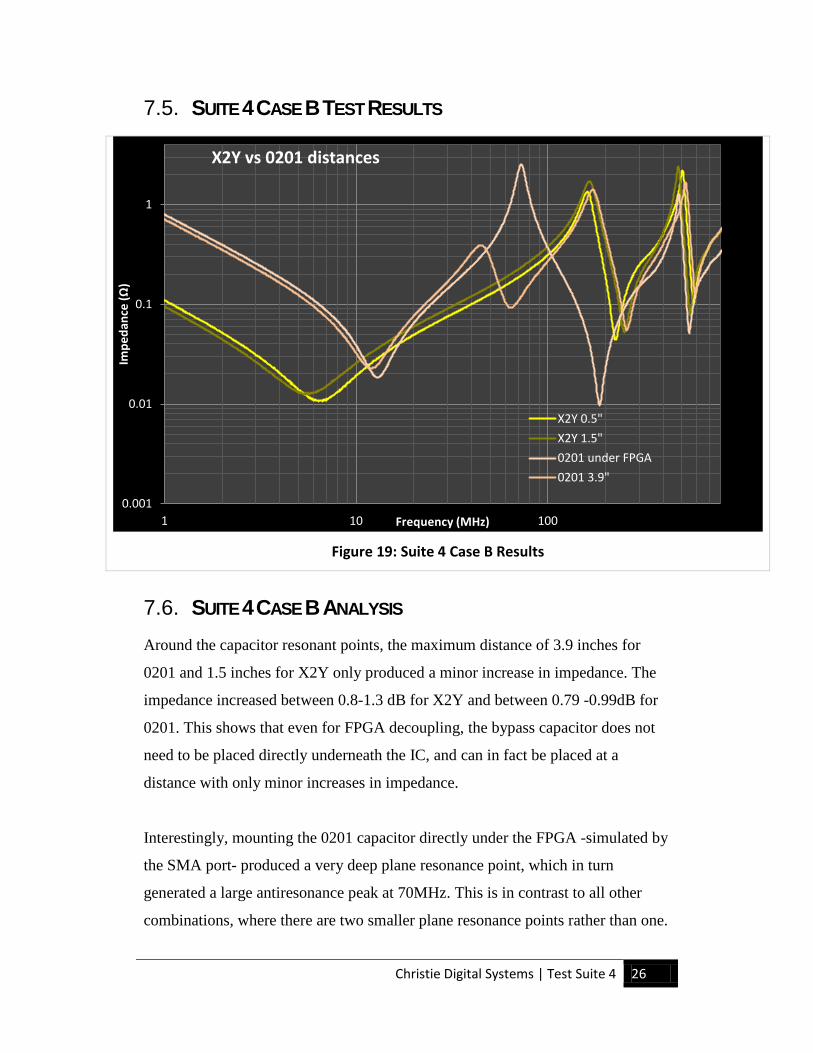
7.5. SUITE 4 CASE B TEST RESULTS
Figure 19: Suite 4 Case B Results
7.6. SUITE 4 CASE B ANALYSIS Around the capacitor resonant points, the maximum distance of 3.9 inches for
0201 and 1.5 inches for X2Y only produced a minor increase in impedance. The
impedance increased between 0.8-1.3 dB for X2Y and between 0.79 -0.99dB for
0201. This shows that even for FPGA decoupling, the bypass capacitor does not
need to be placed directly underneath the IC, and can in fact be placed at a
distance with only minor increases in impedance.
Interestingly, mounting the 0201 capacitor directly under the FPGA -simulated by
the SMA port- produced a very deep plane resonance point, which in turn
generated a large antiresonance peak at 70MHz. This is in contrast to all other
combinations, where there are two smaller plane resonance points rather than one.
0.001
0.01
0.1
1
1 10 100
Impe
danc
e (Ω
)
Frequency (MHz)
X2Y vs 0201 distances
X2Y 0.5" X2Y 1.5" 0201 under FPGA 0201 3.9"
Christie Digital Systems | Test Suite 5 27
8. TEST SUITE 5 8.1. SUITE 5 SPECIFIC OBJECTIVES Suite 5 focused on the Altera PDN tool and how accurate the simulations are to
the real result. This was done in order to determine whether the simulator could
be considered as a tool to assist engineers, or whether it was too inaccurate to be
valuable.
8.2. SUITE 5 PROCEDURE DISTINCTIONS Suite 5 used the same combinations of capacitors as Suite 3 (see Table 2 and
Table 3), which were physically tested using the ITC and VNA, and simulated
using Altera’s PDN tool (version 1.1).
The following parameters were chosen in the PDN tool to best match the
simulation to the tested board:
• No Voltage Regulator Module (VRM) or bulk capacitors
• all capacitor vias on the side with spreading inductance selected to “high”
(tests with low spreading inductance produced a lower correlation)
• PWR-GND distance 4mils using a FR4 PCB dielectric, with a board size
of 5650mils x 2380mils –matching true parameters of the Impedance Test
Card (ITC)
It was anticipated that individual ESR/ESL values could be adjusted to match
vendor-provided values, but repeated requests to Altera to provide the specific
frequency of the ESL/ESR value in their simulation tool were left unanswered.
Christie Digital Systems | Test Suite 5 28
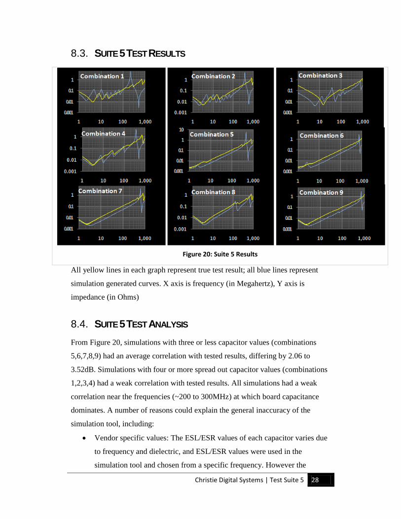
8.3. SUITE 5 TEST RESULTS
Figure 20: Suite 5 Results
All yellow lines in each graph represent true test result; all blue lines represent
simulation generated curves. X axis is frequency (in Megahertz), Y axis is
impedance (in Ohms)
8.4. SUITE 5 TEST ANALYSIS From Figure 20, simulations with three or less capacitor values (combinations
5,6,7,8,9) had an average correlation with tested results, differing by 2.06 to
3.52dB. Simulations with four or more spread out capacitor values (combinations
1,2,3,4) had a weak correlation with tested results. All simulations had a weak
correlation near the frequencies (~200 to 300MHz) at which board capacitance
dominates. A number of reasons could explain the general inaccuracy of the
simulation tool, including:
• Vendor specific values: The ESL/ESR values of each capacitor varies due
to frequency and dielectric, and ESL/ESR values were used in the
simulation tool and chosen from a specific frequency. However the

Christie Digital Systems | Test Suite 5 29
simulation tool did not say what frequency these values are pulled from,
and the answers given from Altera were not helpful.
• Via number: Each capacitor pad had 4 vias, but the simulation only
accounted for 2 (a later test comparison between the simulation and 2 via
test result with one capacitor value showed only a marginal increase in
correlation)
• Inability to accommodate distance: The PDN tool has options to specify
the capacitance, aspect ratio and board design, but it cannot account for
the distance between the bypass capacitor and the IC being bypassed.
Although Suite 2 test results showed that it was fairly low, the large
number of capacitors used combined with the far placement of the
capacitors from the IC resulted in a more significant difference when
comparing simulation to test result.
• For reasons still uncertain, the tested plane had 2 resonant points, but the
simulation had only 1.
Christie Digital Systems | Conclusions 30
9. CONCLUSIONS 1. Changing Mounting Inductance by changing the number of vias has a
moderate effect on a 4 mil board
Suite 1 showed that halving the number of vias matched predictions and
increased impedance by 1.0dB on a 4 mil board. This decrease in
impedance by using 4 vias instead of 2 is beneficial, but the extra vias
increase cost and reduce available board space and may not be
recommended -depending on the target board size and cost.
2. Highest Value Smallest Package is the most effective bypassing rule of
thumb
The results in Suite 3 clearly show that Highest Value Smallest package is
the most effective approach out of all the bypass rules of thumb tested,
providing the lowest impedance across the widest frequency range. The
downside is that when using only MLCC’s, there is a higher component
and layout cost.
3. X2Y capacitors have low ESL and ESR values and can be effectively
used to replace MLCC’s in bypassing applications.
Test suite 3 shows that the best results can be achieved using X2Y
capacitors only. Furthermore out of the Highest Value Smallest Package
combinations, the combination that uses only X2Y capacitors is the
cheapest and takes up the least amount of board space. Suite 4 shows this
dominance still exists even with the highest value smallest package rule of
thumb involved: a single X2Y capacitor performs as well as three 0402 or
0603 capacitors mounted in parallel.

Christie Digital Systems | Conclusions 31
4. Spreading Inductance on a 4 mil board is not a significant contributor
to PCB power line impedance
Test Suite 2 shows that the increase in spreading inductance due to greater
distance between the bypass capacitor and the IC/point of load is not high
enough to have a major effect on the impedance profile. Suite 2 also
shows that transitioning from a 4 mil to 2 mil board does not increase the
spreading inductance by a significant amount.
5. PDN simulation tools are not accurate enough to replace board
prototyping
Although similar, the test results from Suite 5 shows that PDN simulation
programs such as Altera’s “PDN tool” are unable to compensate for
spreading inductance, change in via number and the correct ESL/ESR
values. Without these abilities the tool will continue to be inaccurate and
unreliable, especially with three or more capacitance values.
Christie Digital Systems | Recommendations 32
10. RECOMMENDATIONS 10.1. CAPACITOR SELECTION
1. On boards with tight space requirements, X2Y capacitors are
preferred choice of bypass capacitor, otherwise use multiple 0201’s
When deciding which capacitors should be used for bypassing, electrical
engineers should take into account the amount of space available, as well
as the cost. PCB’s with low cost targets and large amount of available
space should use multiple 0201 bypass capacitors, as they are cheaper
than X2Y capacitors. However PCB’s with little space or very sensitive
IC’s should use X2Y capacitors, as they are capable of providing the
lowest possible impedance for the widest frequency range.
2. When selecting bypass capacitors, follow the Highest Value Smallest
Package Rule
Electrical engineers should select the highest capacitance value in the
smallest possible aspect ratio. For example if the smallest possible
package size available is 0402, then the engineer should use capacitors
with a capacitance of 1μF.
3. Use the simulation tool as a starting point
In spite of its shortcomings, the simulation tool is a helpful guide in
preliminary capacitor selection and can be used as a starting point.
Accuracy can be improved if the engineer enters the vendor-specific ESL
and ESR values into the tool.
Christie Digital Systems | Recommendations 33
10.2. BOARD DESIGN 1. Use 4 vias whenever space permits
PCB designers should try to include 4 vias when connecting the capacitor
pads to the PWR and GND planes in order to reduce mounting inductance.
2. Bypass capacitors should be ideally placed close to the PWR pin of the
IC, but this is not crucial and they can be placed within 4 inches of the
PWR pin with minimal consequences.
PCB designers should not be concerned nor actively focus on placing
bypass capacitors close to the PWR pin of the IC they are trying to bypass,
as the spreading inductance due to the distance is not significant under 4
inches. Capacitor pads should be laid out last on the PCB, after signal
traces and other board elements have been optimized.
3. Do not use 2 mil boards and stay with 4 mil boards: unless there are
benefits in a 2 mil board outside of PDN bypassing applications.
2 mil PCB’s are more expensive and provide little benefit to improving the
bypassing of IC’s. 4 mil boards perform adequately.
10.3. FUTURE STEPS 1. Test Via on Inside (VOI)
The Impedance Test Card had capacitor pads with vias placed on the side
(VOS) in order to reduce the mounting inductance. Vias placed on the
inside –between each capacitor pad- will further reduce the mounting
inductance and should be tested.
2. Test more varied PWR-GND plane distances
4 mil and 2 mil boards were tested, but larger PWR-GND plane distances
should be tested in order to explore the possibility of even lower costs.
Christie Digital Systems | Recommendations 34
3. Test other capacitor technologies
Other capacitor technologies such as Low Impedance Ceramic Capacitors
(LICC’s), Land Grid Array (LGA) and Inter-Digitated Capacitor (IDC)
have been often advertised as having very low ESL and strong high-
frequency performance (Sullivan, 2007). These other capacitor
technologies should be tested in order to assess their impedance-frequency
behaviour.
4. Find equipment capable of performing probing
The ability to test and improve PCB’s that are actually used in products
(and not just purpose-built test boards) would allow for substantially
improved bypassing as the PCB capacitor selection and layout can be
customized for each application. To accomplish this, a Vector Network
Analyzer is needed with specialized probing instruments capable of
performing impedance analysis without a dedicated SMA port.
0.01
0.1
1
1 10 100
Impe
danc
e (Ω
)
Frequency (MHz)
Mounting position
0.5" 4mil
3.9" 4mil
0.5" 2mil
3.9" 2mil
Christie Digital Systems | References 35
11. REFERENCES 1. Agilent Technologies (2007). “Ultra Low Impedance Measurements using
2 Port Measurements”. Agilent Technologies Application Notes [PDF].
Available: http://cp.literature.agilent.com/litweb/pdf/5989-5935EN.pdf
[Accessed: 2011-05-06]
2. Altera Corporation (unknown). “Board Design Guidelines Solution
Center”. Board Design Resource Center [HTML]. Available:
http://www.altera.com/technology/signal/board-design-guidelines/sgl-bdg-
index.html [Accessed: 2011-05-20]
3. Guinta, S. (unknown). “Ask the Applications Engineer – Capacitance and
Capacitors”. Analogue Dialogue Newsletter. [HTML] Available:
http://www.analog.com/library/analogDialogue/Anniversary/21.html
[Accessed: 2011-05-12]
4. Kundert, K. (2004). “Power Supply Noise Reduction”. The Designer’s
Guide Community [PDF]. Available: http://www.designers-
guide.org/Design/bypassing.pdf [Accessed: 2011-06-13]
5. Murata electronics (unknown). “SimSurfing” Murata Software [HTML].
Available: http://ds.murata.co.jp/software/simsurfing/en-us/index.html
[Accessed: 2011-05-17]
6. Schmitz, T. And Wong, M. (2007). “Choosing and Using Bypass
capacitors”. Intersil application note AN1325.0. [PDF] Available:
http://www.intersil.com/data/an/an1325.pdf [Accessed: 2011-05-16]
7. Sullivan, T. (2007). “Choosing Decoupling Capacitors”. Hearst
Electronics Products Technical Articles [HTML]. Available:
http://www2.electronicproducts.com/Choosing_bypass_capacitors-article-
farr_avx_dec2007-html.aspx [Accessed: 2011-05-31]
Christie Digital Systems | Appendix A: Background Information 36
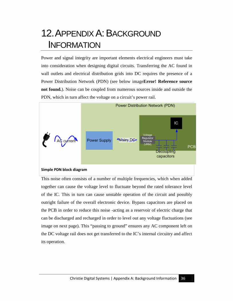
12. APPENDIX A: BACKGROUND INFORMATION
Power and signal integrity are important elements electrical engineers must take
into consideration when designing digital circuits. Transferring the AC found in
wall outlets and electrical distribution grids into DC requires the presence of a
Power Distribution Network (PDN) (see below imageError! Reference source
not found.). Noise can be coupled from numerous sources inside and outside the
PDN, which in turn affect the voltage on a circuit’s power rail.
Simple PDN block diagram
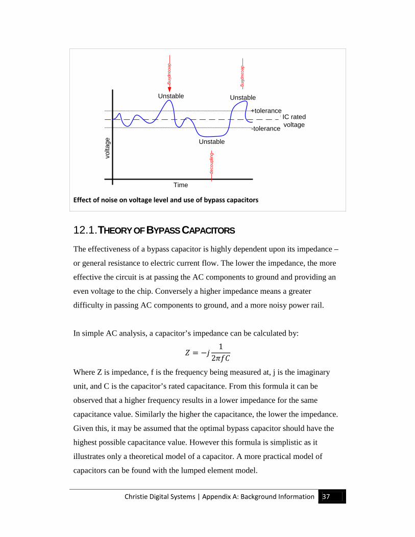
This noise often consists of a number of multiple frequencies, which when added
together can cause the voltage level to fluctuate beyond the rated tolerance level
of the IC. This in turn can cause unstable operation of the circuit and possibly
outright failure of the overall electronic device. Bypass capacitors are placed on
the PCB in order to reduce this noise -acting as a reservoir of electric charge that
can be discharged and recharged in order to level out any voltage fluctuations (see
image on next page). This “passing to ground” ensures any AC component left on
the DC voltage rail does not get transferred to the IC’s internal circuitry and affect
its operation.
Christie Digital Systems | Appendix A: Background Information 37
volta
ge
Time
Unstable
Unstable Unstable
IC rated voltage
+tolerance
-tolerance
decoupling
deco
uplin
g
decoupling
Effect of noise on voltage level and use of bypass capacitors
12.1. THEORY OF BYPASS CAPACITORS The effectiveness of a bypass capacitor is highly dependent upon its impedance –
or general resistance to electric current flow. The lower the impedance, the more
effective the circuit is at passing the AC components to ground and providing an
even voltage to the chip. Conversely a higher impedance means a greater
difficulty in passing AC components to ground, and a more noisy power rail.
In simple AC analysis, a capacitor’s impedance can be calculated by:
𝑍 = −𝑗1
2𝜋𝑓𝐶
Where Z is impedance, f is the frequency being measured at, j is the imaginary
unit, and C is the capacitor’s rated capacitance. From this formula it can be
observed that a higher frequency results in a lower impedance for the same
capacitance value. Similarly the higher the capacitance, the lower the impedance.
Given this, it may be assumed that the optimal bypass capacitor should have the
highest possible capacitance value. However this formula is simplistic as it
illustrates only a theoretical model of a capacitor. A more practical model of
capacitors can be found with the lumped element model.
Christie Digital Systems | Appendix A: Background Information 38
12.1.1. LUMPED ELEMENT MODEL
Similar to how a mass spring damper model allows for the simplification of
complex non-ideal mechanical systems, an electrical lumped element model
allows for the simplification of an electrical circuit into basic components (such as
resistors, voltage/current sources, etc.). These basic components allow for
parasitic -or non ideal- elements of the circuit to be modelled using theoretical
symbols.
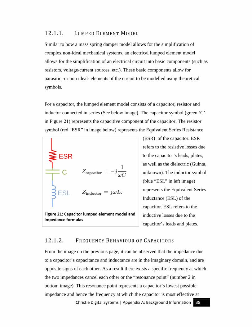
For a capacitor, the lumped element model consists of a capacitor, resistor and
inductor connected in series (See below image). The capacitor symbol (green ‘C’
in Figure 21) represents the capacitive component of the capacitor. The resistor
symbol (red “ESR” in image below) represents the Equivalent Series Resistance
(ESR) of the capacitor. ESR
refers to the resistive losses due
to the capacitor’s leads, plates,
as well as the dielectric (Guinta,
unknown). The inductor symbol
(blue “ESL” in left image)
represents the Equivalent Series
Inductance (ESL) of the
capacitor. ESL refers to the
inductive losses due to the
capacitor’s leads and plates.
12.1.2. FREQUENCY BEHAVIOUR OF CAPACITORS
From the image on the previous page, it can be observed that the impedance due
to a capacitor’s capacitance and inductance are in the imaginary domain, and are
opposite signs of each other. As a result there exists a specific frequency at which
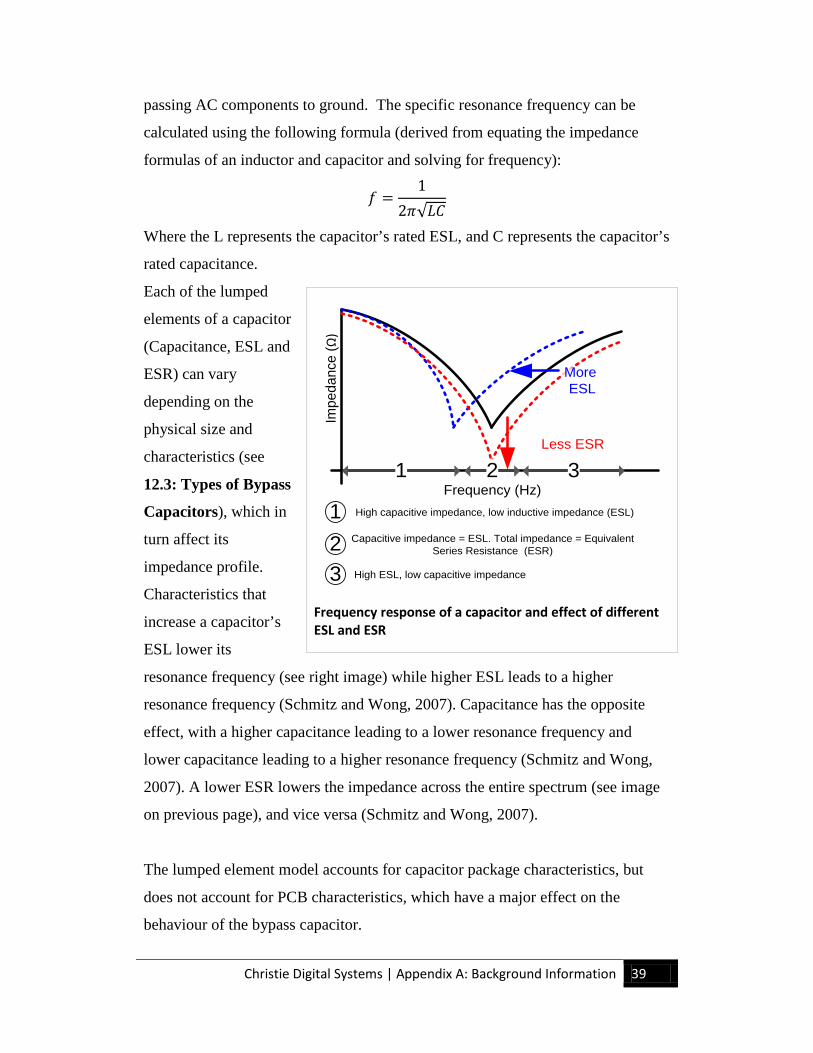
the two impedances cancel each other or the “resonance point” (number 2 in
bottom image). This resonance point represents a capacitor’s lowest possible
impedance and hence the frequency at which the capacitor is most effective at
ESR
C
ESL
Figure 21: Capacitor lumped element model and impedance formulas
Christie Digital Systems | Appendix A: Background Information 39
passing AC components to ground. The specific resonance frequency can be
calculated using the following formula (derived from equating the impedance
formulas of an inductor and capacitor and solving for frequency):
𝑓 =1
2𝜋√𝐿𝐶
Where the L represents the capacitor’s rated ESL, and C represents the capacitor’s
rated capacitance.
Each of the lumped
elements of a capacitor
(Capacitance, ESL and
ESR) can vary
depending on the
physical size and
characteristics (see
12.3: Types of Bypass
Capacitors), which in
turn affect its
impedance profile.
Characteristics that
increase a capacitor’s
ESL lower its
resonance frequency (see right image) while higher ESL leads to a higher
resonance frequency (Schmitz and Wong, 2007). Capacitance has the opposite
effect, with a higher capacitance leading to a lower resonance frequency and
lower capacitance leading to a higher resonance frequency (Schmitz and Wong,
2007). A lower ESR lowers the impedance across the entire spectrum (see image
on previous page), and vice versa (Schmitz and Wong, 2007).
The lumped element model accounts for capacitor package characteristics, but
does not account for PCB characteristics, which have a major effect on the
behaviour of the bypass capacitor.
1Frequency (Hz)
Impe
danc
e (Ω
)
More ESL
Less ESR
23
High capacitive impedance, low inductive impedance (ESL)
Capacitive impedance = ESL. Total impedance = Equivalent Series Resistance (ESR)
High ESL, low capacitive impedance
1 2 3
Frequency response of a capacitor and effect of different ESL and ESR
Christie Digital Systems | Appendix A: Background Information 40
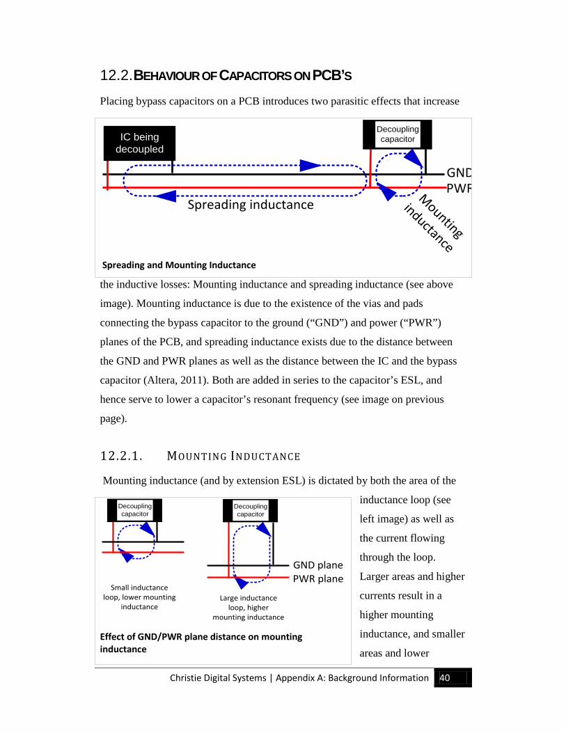
12.2. BEHAVIOUR OF CAPACITORS ON PCB’S Placing bypass capacitors on a PCB introduces two parasitic effects that increase
the inductive losses: Mounting inductance and spreading inductance (see above
image). Mounting inductance is due to the existence of the vias and pads
connecting the bypass capacitor to the ground (“GND”) and power (“PWR”)
planes of the PCB, and spreading inductance exists due to the distance between
the GND and PWR planes as well as the distance between the IC and the bypass
capacitor (Altera, 2011). Both are added in series to the capacitor’s ESL, and
hence serve to lower a capacitor’s resonant frequency (see image on previous
page).
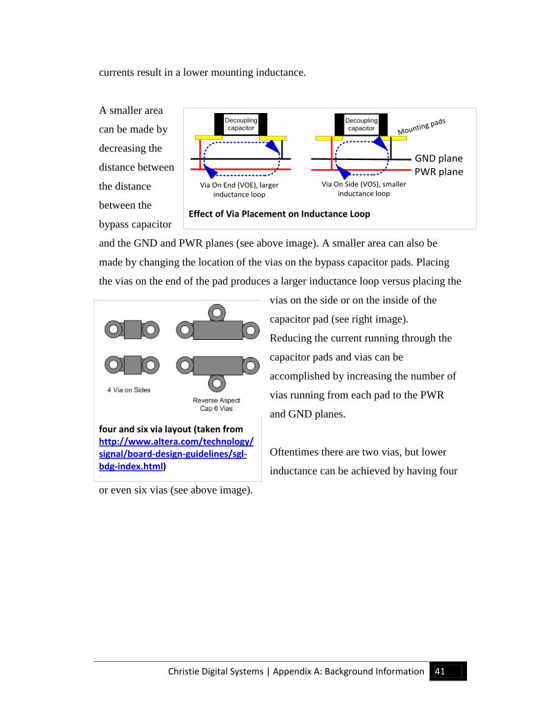
12.2.1. MOUNTING INDUCTANCE
Mounting inductance (and by extension ESL) is dictated by both the area of the
inductance loop (see
left image) as well as
the current flowing
through the loop.
Larger areas and higher
currents result in a
higher mounting
inductance, and smaller
areas and lower
Decoupling capacitor
GND plane PWR planeMounting
inductance
Spreading inductance
IC being decoupled
Spreading and Mounting Inductance
Decoupling capacitor
GND planePWR plane
Small inductance loop, lower mounting
inductance
Decoupling capacitor
Large inductance loop, higher
mounting inductance Effect of GND/PWR plane distance on mounting inductance
Christie Digital Systems | Appendix A: Background Information 41
currents result in a lower mounting inductance.
A smaller area
can be made by
decreasing the
distance between
the distance
between the
bypass capacitor
and the GND and PWR planes (see above image). A smaller area can also be
made by changing the location of the vias on the bypass capacitor pads. Placing
the vias on the end of the pad produces a larger inductance loop versus placing the
vias on the side or on the inside of the
capacitor pad (see right image).
Reducing the current running through the
capacitor pads and vias can be
accomplished by increasing the number of
vias running from each pad to the PWR
and GND planes.
Oftentimes there are two vias, but lower
inductance can be achieved by having four
or even six vias (see above image).
Decoupling capacitor
GND planePWR plane
Via On End (VOE), larger inductance loop
Via On Side (VOS), smaller inductance loop
Decoupling capacitor
Mounting pads
Effect of Via Placement on Inductance Loop
four and six via layout (taken from http://www.altera.com/technology/signal/board-design-guidelines/sgl-bdg-index.html)
Christie Digital Systems | Appendix A: Background Information 42
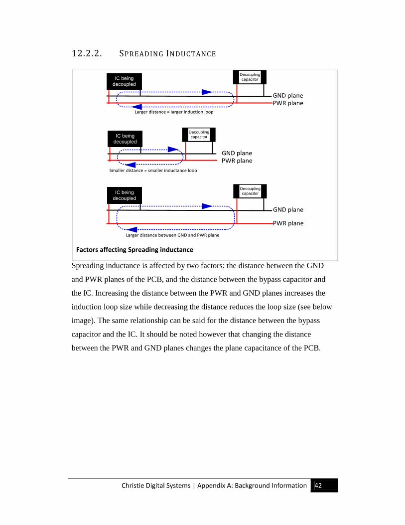
12.2.2. SPREADING INDUCTANCE
Spreading inductance is affected by two factors: the distance between the GND
and PWR planes of the PCB, and the distance between the bypass capacitor and
the IC. Increasing the distance between the PWR and GND planes increases the
induction loop size while decreasing the distance reduces the loop size (see below
image). The same relationship can be said for the distance between the bypass
capacitor and the IC. It should be noted however that changing the distance
between the PWR and GND planes changes the plane capacitance of the PCB.
Decoupling capacitor
GND plane PWR plane
Larger distance = larger induction loop
IC being decoupled
Decoupling capacitor
GND plane PWR plane
Smaller distance = smaller inductance loop
IC being decoupled
Decoupling capacitor
GND plane
PWR plane
Larger distance between GND and PWR plane
IC being decoupled
Factors affecting Spreading inductance
Christie Digital Systems | Appendix A: Background Information 43
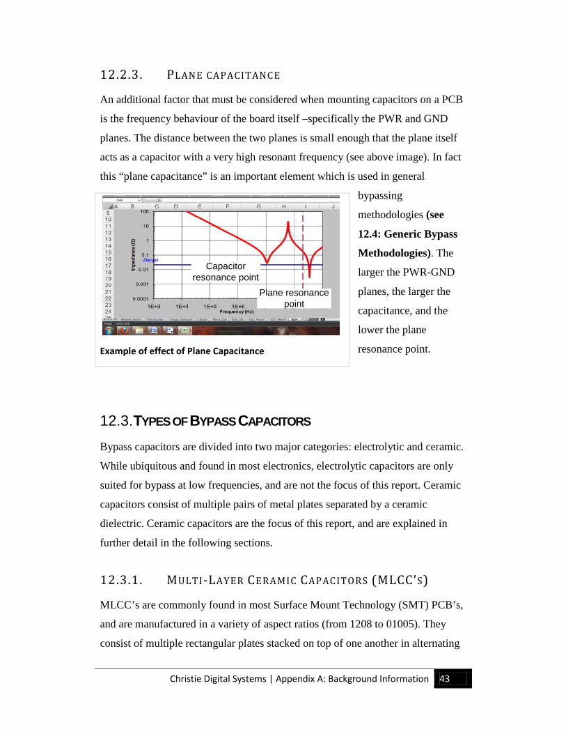
12.2.3. PLANE CAPACITANCE
An additional factor that must be considered when mounting capacitors on a PCB
is the frequency behaviour of the board itself –specifically the PWR and GND
planes. The distance between the two planes is small enough that the plane itself
acts as a capacitor with a very high resonant frequency (see above image). In fact
this “plane capacitance” is an important element which is used in general
bypassing
methodologies (see
12.4: Generic Bypass
Methodologies). The
larger the PWR-GND
planes, the larger the
capacitance, and the
lower the plane
resonance point.
12.3. TYPES OF BYPASS CAPACITORS Bypass capacitors are divided into two major categories: electrolytic and ceramic.
While ubiquitous and found in most electronics, electrolytic capacitors are only
suited for bypass at low frequencies, and are not the focus of this report. Ceramic
capacitors consist of multiple pairs of metal plates separated by a ceramic
dielectric. Ceramic capacitors are the focus of this report, and are explained in
further detail in the following sections.
12.3.1. MULTI-LAYER CERAMIC CAPACITORS (MLCC’S)
MLCC’s are commonly found in most Surface Mount Technology (SMT) PCB’s,
and are manufactured in a variety of aspect ratios (from 1208 to 01005). They
consist of multiple rectangular plates stacked on top of one another in alternating
Capacitor resonance point
Plane resonance point
Example of effect of Plane Capacitance
Christie Digital Systems | Appendix A: Background Information 44
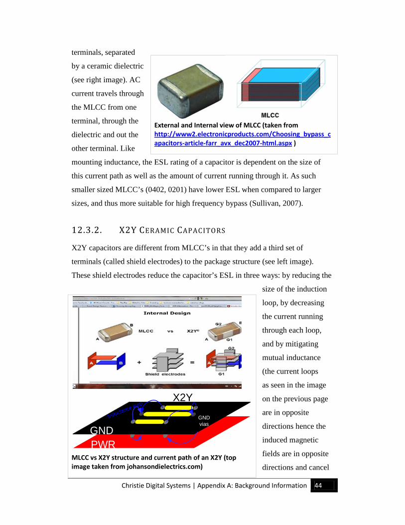
terminals, separated
by a ceramic dielectric
(see right image). AC
current travels through
the MLCC from one
terminal, through the
dielectric and out the
other terminal. Like
mounting inductance, the ESL rating of a capacitor is dependent on the size of
this current path as well as the amount of current running through it. As such
smaller sized MLCC’s (0402, 0201) have lower ESL when compared to larger
sizes, and thus more suitable for high frequency bypass (Sullivan, 2007).
12.3.2. X2Y CERAMIC CAPACITORS
X2Y capacitors are different from MLCC’s in that they add a third set of
terminals (called shield electrodes) to the package structure (see left image).
These shield electrodes reduce the capacitor’s ESL in three ways: by reducing the
size of the induction
loop, by decreasing
the current running
through each loop,
and by mitigating
mutual inductance
(the current loops
as seen in the image
on the previous page
are in opposite
directions hence the
induced magnetic
fields are in opposite
directions and cancel
External and Internal view of MLCC (taken from http://www2.electronicproducts.com/Choosing_bypass_capacitors-article-farr_avx_dec2007-html.aspx )
GNDPWR
Inductance loopX2Y
GND vias
MLCC vs X2Y structure and current path of an X2Y (top image taken from johansondielectrics.com)
Christie Digital Systems | Appendix A: Background Information 45
each other). The result is a capacitor that is advertised to have very low ESL and a
much higher resonant frequency.
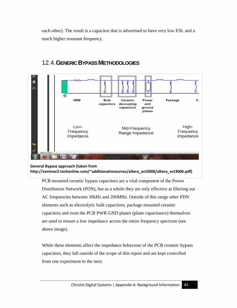
12.4. GENERIC BYPASS METHODOLOGIES
PCB mounted ceramic bypass capacitors are a vital component of the Power
Distribution Network (PDN), but as a whole they are only effective at filtering out
AC frequencies between 30kHz and 200MHz. Outside of this range other PDN
elements such as electrolytic bulk capacitors, package mounted ceramic
capacitors and even the PCB PWR-GND planes (plane capacitance) themselves
are used to ensure a low impedance across the entire frequency spectrum (see
above image).
While these elements affect the impedance behaviour of the PCB ceramic bypass
capacitors, they fall outside of the scope of this report and are kept controlled
from one experiment to the next.
General Bypass approach (taken from http://seminar2.techonline.com/~additionalresources/altera_oct3006/altera_oct3006.pdf)