improving mlc flash performance and endurance with extended...
TRANSCRIPT

Improving MLC flash performance and endurancewith Extended P/E Cycles
Fabio MargagliaJohannes Gutenberg-Universitat
Mainz, GermanyEmail: [email protected]
Andre BrinkmannJohannes Gutenberg-Universitat
Mainz, GermanyEmail: [email protected]
Abstract—The traditional usage pattern for NAND flash memoryis the program/erase (P/E) cycle: the flash pages that make aflash block are all programmed in order and then the whole flashblock needs to be erased before the pages can be programmedagain. The erase operations are slow, wear out the medium,and require costly garbage collection procedures. Reducing theirnumber is therefore beneficial both in terms of performanceand endurance. The physical structure of flash cells limits thenumber of opportunities to overcome the 1 to 1 ratio betweenprogramming and erasing pages: a bit storing a logical 0 cannotbe reprogrammed to a logical 1 before the end of the P/E cycle.
This paper presents a technique to minimize the number oferase operations called extended P/E cycle. With extended P/Ecycles, the flash pages can be programmed many times beforethe whole flash block needs to be erased, reducing the number oferase operations. We study the applicability of the technique toMulti Level Cell (MLC) NAND flash chips, and present a designand implementation on the OpenSSD prototyping board. Theevaluation of our prototype shows that this technique can achieveerase operations reduction as high as 85%, with latency speedupsof up to 67%, with respect to a FTL with traditional P/E cycles,and naive greedy garbage collection strategy. Our evaluation leadsto valuable insights on how extended P/E cycles can be exploitedby future applications.
I. INTRODUCTION
NAND flash memory is currently the solid state technologymost widely used in storage systems, mainly packaged asSolid State Drives (SSD). It offers great read and writeperformance, and a low power consumption. Despite thesesubstantial improvements relative to hard disk drives (HDD),the gap in cost per gigabyte still limits the adoption of SSDs asreplacements for HDDs. Flash manufacturers try to drive downcosts by storing more bits per flash cell to increase its density,introducing Multi Level Cell (MLC) flash. This technologyuses cells with 4 or 8 states (respectively 2 or 3 bits per cell),as opposed to Single Level Cell (SLC) flash, which has 2states (1 bit per cell). In this paper we focus on MLC chipswith 4 states which are the most common in both consumerand enterprise SSDs.
Every state is characterized by a threshold voltage (Vth). Whenmore bits are packed in a flash cell the Vth margins betweendifferent states are reduced and the processes required to detectthe difference need to be more precise, and consequentlybecome slower and more prone to errors. Therefore, whileflash density increases rapidly, all other critical metrics –
performance, endurance, and data retention – decrease ata higher pace. The metric showing the steepest and mostalarming decline is the endurance. A recent study on 45 flashchips shows that each additional bit per flash cell reduces theexpected lifetime by up to 20x [1].
The major cause of the limited lifetime in flash technology isthe cell wear out caused by the erase operation. This operationis required to bring the flash cells to their initial state, whichcorresponds to the lowest Vth. Since a program operation canonly increase the Vth of a cell, the cell must be erased beforebeing programmed again, so that the cell can be set to anarbitrary state. Hence, the traditional usage of flash memory inthe program/erase cycles (P/E cycles). An approach to reducethe erase operations is that of reprogramming the flash bitswithout erasing them first, sacrificing the possibility to reachstates with lower Vth. In this paper we refer to this techniqueas extended P/E cycles because it allows multiple programoperations per cycle. Theoretical studies and simulations ofthis approach have been presented in [2]–[4].
Performing multiple program operations per cycle has theconstraint that the reprogrammed cells cannot be set to anarbitrary value. The previous work in this area is based on theassumption that flash cells can be safely programmed multipletimes as long as the bits are flipped in a single direction (e.g.1→0). In this paper we refer to this assumption as the write-once memory constraint (WOM constraint), and to data thatcomplies with it as WOM compatible. The WOM constraintwas based on the behavior of punched cards and optical disks,but applies to today’s flash SLC chips as well because theyhave only two states. Previous work shows how to achieveWOM compatible data patterns through encodings [5], orspecialized data structures [3].
However, the WOM constraint can not be applied directly toMLC flash, because every cell is characterized by 4 states,encoded into 2 bits. Therefore, when a bit is reprogrammed,the state of the flash cell is modified, possibly corrupting thevalue of the other bit. This phenomenon happens also whenthe bits are flipped according to the WOM constraint, and iscalled program disturbance [6].
In this paper we address the applicability of extended P/Ecycles to MLC flash. Our main contribution is the identificationand definition of the additional constraints imposed by MLCtechnology, which we refer to as the practical MLC WOMconstraints. We present these constraints in a state diagram.
978-1-4673-7619-8/15/$31.00 c©2015 IEEE

Vth
11 01 00 10
R1 R2 R3
1 0
R1
SLC MLC
Vth
Fig. 1. Distributions of threshold voltages for SLC and MLC. Eachdistribution shows the logical bits that it represents. R0, R1, R2, R3 are theread points. Due to wear out the Vth distributions change over the lifetime ofa cell. A cell becomes unreadable when the distributions cross the read points.
While WOM compatible MLC reprogramming has been dis-cussed in [6], to the best of our knowledge this is the firstpresentation of such a diagram with detailed information ofall possible state transitions. We believe that this tool willbe useful to system designers and coding theorists for furtheroptimizations of the flash utilization. In this work we choseto use only the WOM compatible state transitions to design aFlash Translation Layer (FTL) that uses extended P/E cycleswithout sacrificing flash capacity. All previous FTL designswere based on SLC flash [2], or on simulations that did notconsider the MLC constraints [4], [7]. We implemented andevaluated our FTL design using the OpenSSD platform [8],which is an experimental kit for SSD design and developmentequipped with 35 nm MLC chips.
The rest of this paper is structured as follows: Section II intro-duces the main concepts concerning flash and FTLs, and givesthe background on WOM codes and WOM-compatible datastructures. Section III presents the state diagram for a typicalMLC flash cell. Section IV describes the FTL implementation,and Section V presents its evaluation. Section VI presents therelated work, and Section VII concludes.
II. BACKGROUND
A. Flash Operations
A flash chip consists of an array of cells. Each cell is atransistor with a floating gate that can retain electrons. Thecell’s state depends on the number of electrons in the floatinggate because they hinder the normal behavior of the transistor,increasing the threshold voltage (Vth) required to activate it.Therefore, a cell’s state can be determined by probing thevoltage required to activate the transistor.
The floating gate’s electron population can be altered with twooperations: the flash program operation injects new electrons,while the erase operation depletes the floating gate completely.Vth can be probed with the read operation. The cells are readand programmed in pages of size ranging from 8 KB to 32 KB,and are erased in blocks of 2 MB to 4 MB.
Program operations can only increase the cell’s state, thereforeany attempt to reprogram a page will fail if a cell’s stateshould decrease as a result of the operation. In the generalcase, in-place page updates are prohibited, and the pages mustbe erased and then programmed again, hence the traditionalProgram/Erase cycles (P/E) usage pattern.
Block
0 21 3 4 5 6126
125
127
124
123
...: High Page
: Low Page
Fig. 2. Low and High pages in a block. The arrows show the couples thatshare the same flash cells and are thus influenced when programming eachother.
B. SLC and MLC
Depending on the precision of the machinery necessary toprobe the threshold voltage, it is possible to distinguish be-tween more states per flash cell. As shown in Figure 1, SingleLevel Cells (SLCs) distinguish between 2 states, while MultiLevel Cells (MLCs) distinguish between 4 states. Therefore,each SLC represents 1 bit of information, while each MLCrepresents 2 bits.
Every MLC has 4 levels encoded into 2 bits. The two bits ofa MLC are mapped to two independently accessible logicalpages, called low page and high page. Therefore, when eitherof these two pages is programmed, the Vth of the cell increases,changing the cell’s state and possibly the value of the other bit.However, the flash manufacturers guarantee that if the low pageis programmed first, and the high page later, the two operationswill be successful and will not influence one another.
Figure 2 shows the configuration of low and high pages inthe chips we analyzed. Grupp et al. presented an analysis ofdifferent chips in [6] that shows that all the chips they testedare configured in a similar way, if not identical. Note that, withthis configuration, programming the pages in order implies thatthe low page is always programmed before the high page.
C. Flash Translation Layer
The Flash Translation Layer (FTL) is a dedicated firmware,that runs on the controller of the SSDs, that is responsible formanaging the flash chips. It has to convert the host requestsinto flash operations, and is optimized to handle the lack ofin-place updates, and the big size of erase blocks. It commonlystructures the available flash memory as a log of pages. Thein-place updates are avoided by appending the updated pageto the log. A mapping table is maintained by the FTL to keeptrack of these page remappings.
The log structure requires garbage collection because theremapping of pages leaves stale copies that accumulate duringthe log lifetime. The garbage collection process scans the flashfor a victim erase block, copies the valid pages containedtherein to the end of the log, and erases the block. The victimblock selection affects performance because it determines howmuch data has to be copied. The popular greedy strategychooses the block with the lowest amount of valid data [9].Other strategies have been proposed, which consider the hot-ness and age of the data [10].
D. OpenSSD
The platform we use to implement our prototype isthe OpenSSD prototyping kit that hosts an Indilinx

TABLE I. TWO GENERATIONS WOM CODE
Plain bits 1st gen 2nd gen00 111 00001 110 00110 101 01011 011 100
BarefootTMcontroller, and eight slots for custom flash mod-ules [8]. Each module hosts four 64 Gb 35 nm MLC flash chips,for a total of 32 GB of flash memory per module. The flashchips have a page size of 32 KB, and erase blocks made of128 pages (4 MB). Every page has 512 extra bytes referred toas spare region. This region is meant to be used to store FTLmetadata. However, in the OpenSSD board, the spare regionis not directly accessible by the controller.
E. Bit Errors and ECC
During their lifetime, the flash cells are subject to wear-out. The repeated injections and removals of electrons in thefloating gate ruin the physical structure of the cell, leadingto its malfunction. This causes bit errors in the flash pages.Typically error correction codes (ECC) are used to improvethe reliability of flash.
The OpenSSD platform is shipped with a hardware acceleratorthat transparently computes the ECC and stores it in the spareregion at each flash program operation. This behavior can notbe modified, and the spare region can not be accessed by thecontroller. This ECC can correct up to 12 B per 512 B segment.When the controller issues a flash page read operation thehardware accelerator corrects the bit errors on the fly duringthe operation. When the page contains more errors than canbe corrected, the hardware accelerator raises an incorrectableerror interrupt to the controller, and leaves the data untouched.
For the sake of the analysis presented in this paper it wasimportant to circumvent the ECC to observe the raw behaviorof the cells when using the extended P/E cycles. Unfortunately,due to limitations of the OpenSSD board, we could not disablethe ECC protection when writing entire pages. We could,however, disable the ECC protection when performing partialpage write operations of only 512 B. This limitation influencedthe set up of two experiments presented in this work: theanalysis of the reprogram operation in MLC (Section III), andthe bit error rate evaluation (Section V-A).
F. Page reprogramming in SLC
SLCs map the low Vth state to a logical 1, and the high Vth
state to a logical 0 (see Figure 1). Therefore, a page can bereprogrammed with new data if all the bits are flipped inthe 1→0 direction, or are not modified, with respect to thebits already contained in the page. We call this the WOMconstraint. The problem of updating data complying with theWOM constraint has been tackled in two ways:
a) WOM codes: WOM codes, introduced by Rivest et al. [5],offer redundant encodings organized in generations, wherethe number of generations is the number of WOM compliantupdates allowed by the code. Table I shows a 2 generationsWOM code scheme that encodes bit pairs into 3 bit codewords. The 0s in each code word of a generation are a supersetof the 0s of all the different code words in the previous
generations. Therefore, every code word can always be updatedto a different code word of the next generation respecting theWOM constraint.
b) WOM compatible data structures: some data structures canbe modified to perform WOM compatible accesses. Kaiser etal. presented a B-Tree with log structured nodes with unsortedentries [3]. The nodes are initialized with all bits set to 1. Thenew entries are appended to the node, in the initialized area,generating only 1→0 bit flips. Bloom filters [11] flip bits ina single direction by construction and are WOM compatiblewithout need of modifications.
G. Program disturbance in MLC
Program disturbance is defined as the involuntary flipping ofone or more bits of a page, that happens as a consequence ofa program operation on a different page. Previous experimentshave shown that reprogramming MLC flash causes programdisturbance. In particular, Grupp et al. showed that reprogram-ming the high page disturbs the bits of the respective low page.On the other hand, reprogramming the low page does not affectthe high page [6].
III. PAGE REPROGRAMMING IN MLC
TABLE II. TRADITIONALVth MAPPING
REPRESENTATION
Vth LB HBMin 1 1
1 00 0
Max 0 1
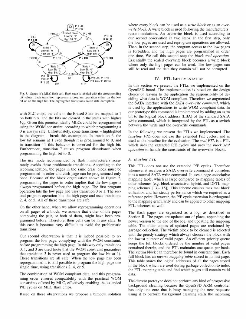
In order to better understand theimplications of the reprogramoperation in MLC flash chips,we extracted the cell’s state dia-gram for a typical MLC, whichis shown in Figure 3. To the bestof our knowledge, this is thefirst time that this informationis presented for MLCs. Previouspublications [3], [12], and theflash manufacturers, show onlya tabular representation of the mapping (Table II). Despiteshowing the same states, the tabular representation lacks thetransitions between them. These transitions are fundamental toidentify the program patterns leading to program disturbanceand data corruption.
The experiment we used to extract the diagram was performedon the OpenSSD board. The procedure consisted of takinga couple of connected low/high pages (see Figure 2) andtraversing every state transition by programming a single bitbelonging either to the low or the high page, and then readingback the content of both pages. In order to correctly detect thecontent after the transition, we needed to avoid any interferenceof the ECC hardware accelerator of the OpenSSD board.Therefore, we disabled it, and to do so we had to use the partialwrite operations of 512 B (the only ones allowed). This was nota problem because our goal was to program a single bit everytime. Once we extracted the complete diagram, we verifiedit with full page write operations. Since the ECC could notbe disabled on full page operations, we made sure to overloadthe ECC correction capacity by flipping more bits than it couldcorrect. The verification with full page operations performedin this way confirmed the diagram.
Our first observation is that there are in fact 5 states rather than4 because the order in which bits are programmed affects thebehavior of the cell in future program operations. Consistently
Erased StateLow Bit: ‘1’High Bit: ‘1’
State 1Low Bit: ‘0’High Bit: ‘1’
State 2Low Bit: ‘1’High Bit: ‘0’
State 3Low Bit: ‘0’High Bit: ‘0’
State 4Low Bit: ‘0’High Bit: ‘1’
P 1 LBP 1 HB
P 0 LB P 0 HB
P 1 HBP 0 HB
P 1 HB
P 0 HB P 1 HB
P 1 LBP 0 LB
P 0 LBP 1 LB
P 0 LB / P 1 HBP 1 LB / P 0 HB
P 0 LBP 0 HBP 1 LB
(1)
(0)
(2)
(3)
(4)
(6)
(5) (7)
(8)
(9)
(10) (11)
Fig. 3. States of a MLC flash cell. Each state is labeled with the correspondingbit values. Each transition represents a program operation either on the lowbit or on the high bit. The highlighted transitions cause data corruption.
with SLC chips, the cells in the Erased State are mapped to 1on both bits, and the bits are cleared in the states with higherVth. Given this premise, ideally MLCs could be reprogrammedusing the WOM constraint, according to which programming a0 is always safe. Unfortunately, some transitions – highlightedin the diagram – break this assumption. In transition 6, thelow bit remains at 1 even though it is programmed to 0, andin transition 11 this behavior is observed for the high bit.Furthermore, transition 7 causes program disturbance whenprogramming the high bit to 0.
The use mode recommended by flash manufacturers accu-rately avoids these problematic transitions. According to therecommendation, the pages in the same erase block must beprogrammed in order and each page can be programmed onlyonce. Because of the block organization shown in Figure 2,programming the pages in order implies that the low page isalways programmed before the high page. The first programoperation hits the low page and uses transition 0 or 1. The sec-ond program operation hits the high page and uses transitions2, 4, or 5. All of these transitions are safe.
On the other hand, when we allow reprogramming operationson all pages of a block, we assume that either of the pagescomposing the pair, or both of them, might have been pro-grammed before. Therefore, their cells can be in any state. Inthis case it becomes very difficult to avoid the problematictransitions.
Our second observation is that it is indeed possible to re-program the low page, complying with the WOM constraint,before programming the high page. In this way only transitions0, 1, and 3 are used (note that the WOM constraint guaranteesthat transition 3 is never used to program the low bit at 1).These transitions are all safe. When the low page has beenreprogrammed it is still possible to program the high page onesingle time, using transitions 2, 4, or 5.
The combination of WOM compliant data, and this program-ming order ensures compatibility with the practical WOMconstraints offered by MLC, effectively enabling the extendedP/E cycles on MLC flash chips.
Based on these observations we propose a bimodal solution
where every block can be used as a write block or as an over-write block. A write block is used following the manufacturers’recommendations. An overwrite block is used according toour second observation in two steps. In the first step, onlythe low pages are used and reprogram operations are allowed.Then, in the second step, the program access to the low pagesis forbidden, and the high pages are programmed in orderone time. We call this second step the block seal operation.Essentially the sealed overwrite block becomes a write blockwhere only the high pages can be used. The low pages canstill be read and the data they contain will not be corrupted.
IV. FTL IMPLEMENTATION
In this section we present the FTLs we implemented on theOpenSSD board. The implementation is based on the designchoice of leaving to the application the responsibility of de-ciding what data is WOM compliant. Therefore we augmentedthe SATA interface with the SATA overwrite command, whichis used by the applications to write WOM compliant data. Inour prototype this command is implemented by adding an extrabit to the logical block address (LBA) of the standard SATAwrite command, which is interpreted by the FTL as a switchbetween the write and the overwrite commands.
In the following we present the FTLs we implemented. Thebaseline FTL does not use the extended P/E cycles, and isused as the baseline for the evaluation. The seal FTL is a FTLwhich uses the extended P/E cycles and uses the block sealoperation to handle the constraints of the overwrite blocks.
A. Baseline FTL
This FTL does not use the extended P/E cycles. Thereforewhenever it receives a SATA overwrite command it considersit as a normal SATA write command. It uses a page-associativemapping table, which is large compared to mapping tables ofother schemes (e.g. block associative, hybrid, and DFTL map-ping schemes [13]–[15]). This scheme ensures maximal blockutilization and has steady performance which we required as areference point. However, the P/E cycle extension is orthogonalto the mapping granularity and can be applied to other mappingFTL schemes as well.
The flash pages are organized as a log, as described inSection II. The pages are updated out of place, appending thenewer version to the end of the log, and updating the mappingtable. The older copies of updated pages are reclaimed bygarbage collection. The victim block to be cleaned is selectedwith the greedy strategy which always chooses the block withthe lowest number of valid pages. An efficient priority queuekeeps the full blocks ordered by the number of valid pagescontained therein, and the FTL maintains one queue per bank.The victim block can therefore be found in constant time. Eachfull block has an inverse mapping table stored in its last page.This table stores the logical addresses of all the pages storedin the block which are used during garbage collection to indexthe FTL mapping table and find which pages still contain validdata.
The current prototype does not perform any kind of progressivebackground cleaning because the OpenSSD ARM controllerhas only one core that is busy managing the new requests:using it to perform background cleaning stalls the incoming

: Reprogrammable page
Seal
: Not reprogrammable page
: Empty page
Full Write Blocks
...
Active Write BlockNext write
page
Full OW Blocks
...
Active OW Block
Next overwrite
page
Clean Blocks
...GC
GCBlkfull
Blkfull
Fig. 4. Life cycle of blocks in the seal FTL. Clean blocks can be chosenas either write blocks or overwrite blocks. For every bank, the FTL maintainsone active write block and one active overwrite block, with a pointer to thenext free page. The low pages in all the overwrite blocks are reprogrammableuntil they are sealed. In the picture the active write block is an overwrite blockwhich has just been sealed. The pointer to the next write page will point onlyto high pages. The garbage collection process can be performed both on fullwrite blocks and full overwrite blocks.
request queue and harms performance. The only optimizationwe implemented consists of polling the priority queues of eachidle bank in search of completely invalid blocks. These blockscan be erased with the asynchronous erase command offeredby the flash chips while processing every SATA request. Toimplement this optimization the queue has been augmentedwith the ability to return the number of valid pages.
The garbage collection procedure is triggered whenever abank contains only one clean block. The victim is chosenbased on the priority queues described before. The garbagecollection copies all the valid pages to the end of the log.We let the garbage collection copy valid data to other banksso that the whole routine is accelerated by parallelizing theprogram operations. The program operations are asynchronous,although the temporary DRAM buffers must be locked untilthe operation completes. The identification of the valid pagesis sped up by the reverse mapping table stored in the last pageof every full block.
The implementation of the garbage collection subroutine thatcopies the valid pages poses an interesting design choice. Theflash chips offer the copyback operation, which is able to copyone entire page to a different page within the same flash bank.Since the data never leaves the bank, this operation is fasterthan reading a page and programming it to a new location.However, we did not employ the copyback operation for tworeasons. First, we hide the cost of the program operation byrunning it asynchronously on the other banks. Second, whenthe copyback operation is used, the data never leaves the bank,therefore the ECC is neither checked on read nor recomputedon write. Any error will be copied to the new page weakeningthe overall protection.
B. Seal FTL
This FTL uses the extended P/E cycles, therefore it has beenextended with the notion of overwrite blocks as described
0613
pageblockbankoverwrite bit
1831
Fig. 5. Physical address stored in the mapping table for a SSD configuredwith 32 banks and 128 blocks per bank.
is Section III. Traditionally, the flash blocks exist in threestates. They can be clean, full, or be the current active blockwhere incoming data is written to. The seal FTL insteaddistinguishes between two main categories of flash blocks:write blocks and overwrite blocks. Therefore, blocks can existin five different states: clean, full write block, full overwriteblock, current active write block, and current active overwriteblock (see Figure 4). In the full overwrite blocks and the activeoverwrite block only the low pages are used, therefore the pagereprogram operation is allowed.
Overwrite Operation
For each request identified as a SATA overwrite commandthe FTL searches the corresponding physical addresses in themapping table. The physical addresses, represented in Figure 5,identify a unique (bank, block, page) tuple. In addition, one bitis reserved for pages residing in full or active overwrite blocks(filled with a checkered pattern in Figure 4). When this bit isset the FTL can proceed reprogramming the page directly inits current physical page. If the bit is not set, or if it is the firsttime that the application addresses the page, the FTL uses thenext low page in the active overwrite block.
The FTL maintains one reprogram counter per page in theDRAM. It is possible to set a limit to the reprogram operationsper page. When a reprogram operation hits a page that reachedthe limit, the FTL uses the next low page in the active overwriteblock instead, and decreases the number of valid pages for thatblock in the priority queue.
Overwrite Block Sealing
When the FTL needs a new block and there is only one blockleft in the clean pool, it can either trigger garbage collection orseal an overwrite block to use its high pages. We will discussthe empirical policy used to take this decision later, here weexplain how the seal operation is implemented.
Once a block is sealed, its pages cannot be reprogrammedanymore. If a future overwrite operation hits one of the pagescontained in the block, the FTL will be forced to find anew physical location for it, losing the overwrite potential.Therefore, the FTL attempts to select the block whose pagesare least likely to be overwritten in the future. To do so,the FTL maintains a priority queue, identical to the one usedfor write blocks, to find the overwrite block with the lowestamount of valid pages in constant time. This block is chosenas a victim. The rationale behind this design is that, havingless valid pages, the probability for a future overwrite hit islower.
When the block is chosen, the FTL needs to clear all theoverwrite bits in the corresponding physical addresses (see

Figure 5). To find them quickly the FTL keeps an inversemapping table containing the logical addresses of all pagesin the block. This inverse mapping table is stored in thelast low page of the block, after all the other low pagesare programmed. During the seal operation, the FTL readsthe inverse mapping table and scans the FTL mapping tableclearing all the overwrite bits of the pages that are still mappedto the block.
Finally, the FTL points the next write page pointer to thefirst high page in the block, and sets the flag that makes thenext write page pointer increase in steps of 2 (according tothe mapping shown in Figure 2). After this point the blockis considered the active write block and its pages cannot bereprogrammed.
Garbage Collection
The garbage collection procedure is similar to the one used inthe baseline FTL. Preferably the victims are full write blockswith a few valid pages, however the procedure works on fulloverwrite blocks, too, with the only difference that the inversemapping table is located in the last low page, i.e. page 125(see Figure 2), instead of the last high page. The inversemapping table for full overwrite blocks has invalid entriescorresponding to all the high pages, therefore the garbagecollection procedure does not perform any operation on them.The following section explains when the garbage collection istriggered on full overwrite blocks.
Victim Selection Policies
The main tool for victim selection are the two priority queuesfor write and overwrite blocks. The preferred victims are fullwrite blocks with few valid pages because they have been usedcompletely, i.e. all the pages have been programmed, and thecleaning cost consists of copying the few valid pages theycontain. In contrast, the full overwrite blocks should be left inthat state for as long as possible, because their pages can bereprogrammed in the future.
However, if only the full write blocks are garbage collected,the full overwrite blocks accumulate, reducing the number ofwrite blocks. Consequently, the garbage collection invocationsbecome more frequent, and the full write blocks are reclaimedearlier, when they still contain a high number of valid pages.
To prevent this, the FTL can choose to seal a full overwriteblock and use its high pages, instead of triggering a garbagecollection. This choice is made when the victim in the over-write priority queue has less valid pages than the victim in thewrite queue. This policy ensures that garbage collections donot have to copy too much data. An overwrite block can, infact, have a maximum of 63 valid pages (the last low page isreserved for the inverse mapping table). Therefore, this is theupper bound for data copying during garbage collection.
The seal operation is not a solution when the FTL needs toallocate a new active overwrite block. This requires an erasedblock, and a garbage collection operation is inevitable. Toprevent using garbage collection on full write blocks withmany valid pages, the FTL can choose to select a full overwriteblock as victim instead, if it has less valid pages. However, thatmeans that the high pages are erased without ever being used.We have experimented with two strategies for victim selection:
• Comparing only the number of valid low pages inthe overwrite blocks, and consider all the high pages(empty) as invalid.
• Comparing the number of valid low pages plus thenumber high pages.
The second option attempts to preserve the overwrite blockfrom being reclaimed, taking into account the fact that thehigh pages could be written after an eventual seal operation.Section V presents an evaluation of both strategies.
ECC
The ECC hardware accelerator of the OpenSSD platform hasa fixed behavior that can not be modified. When a page isprogrammed for the first time, the ECC is computed and storedin a fixed location of the spare area of the flash page. Whenthe page is reprogrammed, a new ECC is computed and storedin the same location of the spare area. Since the ECC is notWOM compliant, this results in a corrupt ECC.
The OpenSSD platform does not offer any possibility tomodify this behavior. Therefore, our prototype does not offerdata protection on reprogrammed pages. However, we envisiontwo possible solutions to this issue:
• Encode the data with a WOM code which offers errorcorrection capabilities [16].
• Use the spare region as append-only log, and appendnewer ECCs after the old ones.
In our evaluation the FTL enforced a per page limit of 8overwrites, to simulate 8 ECCs appended in the spare region,e.g. 8 ECCs of 64 B can be appended in the 512 B spare regionoffered by the flash chips shipped with the OpenSSD. Notethat we did not disable the ECC accelerator when running theevaluation, therefore the ECC computation still happens, andits delay is considered in our experiments. The FTL ignores theECC failure interrupts that occur when reading reprogrammedpages.
V. EVALUATION
A. Impact of Extended P/E Cycles on Lifetime
In this section, we evaluate how the extended P/E cyclestechnique impacts the lifetime of a flash cell. The lifetime isexpressed as the number of P/E cycles that a cell can sustainbefore becoming unusable. The bit error rate (BER) growswith repeated P/E cycles, to the point where the errors foundin a page are too many to be corrected with ECCs. At thatpoint the page can no longer be used safely.
The traditional BER analysis to evaluate the lifetime of acell consists of the repetition of P/E cycles on a single flashblock. During the program, phase every page in the block isprogrammed. During the erase phase, the entire block is erased.The content of the block is checked for errors after every phase,and the number of errors is used to compute the BER. Thisanalysis has been performed by different research groups ondifferent flash chips [1], [2], [6], [17].
To evaluate the effect of the extended P/E cycles on the flashlifetime, we modified the traditional BER analysis to programthe pages multiple times in each program phase.
0 2000 4000 6000 8000 10000 12000Program/Erase cycles
0
2e-4
4e-4
6e-4
8e-4
10e-4
12e-4
14e-4
16e-4
18e-4bi
t err
or ra
te
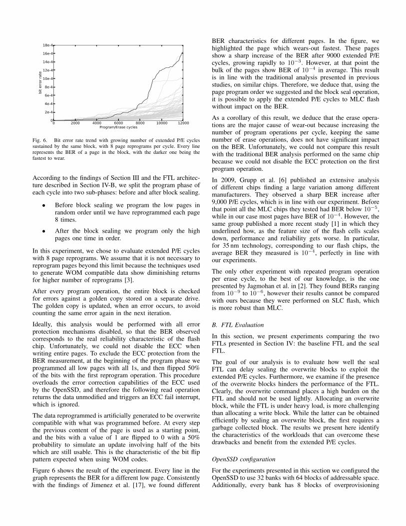
Fig. 6. Bit error rate trend with growing number of extended P/E cyclessustained by the same block, with 8 page reprograms per cycle. Every linerepresents the BER of a page in the block, with the darker one being thefastest to wear.
According to the findings of Section III and the FTL architec-ture described in Section IV-B, we split the program phase ofeach cycle into two sub-phases: before and after block sealing.
• Before block sealing we program the low pages inrandom order until we have reprogrammed each page8 times.
• After the block sealing we program only the highpages one time in order.
In this experiment, we chose to evaluate extended P/E cycleswith 8 page reprograms. We assume that it is not necessary toreprogram pages beyond this limit because the techniques usedto generate WOM compatible data show diminishing returnsfor higher number of reprograms [3].
After every program operation, the entire block is checkedfor errors against a golden copy stored on a separate drive.The golden copy is updated, when an error occurs, to avoidcounting the same error again in the next iteration.
Ideally, this analysis would be performed with all errorprotection mechanisms disabled, so that the BER observedcorresponds to the real reliability characteristic of the flashchip. Unfortunately, we could not disable the ECC whenwriting entire pages. To exclude the ECC protection from theBER measurement, at the beginning of the program phase weprogrammed all low pages with all 1s, and then flipped 50%of the bits with the first reprogram operation. This procedureoverloads the error correction capabilities of the ECC usedby the OpenSSD, and therefore the following read operationreturns the data unmodified and triggers an ECC fail interrupt,which is ignored.
The data reprogrammed is artificially generated to be overwritecompatible with what was programmed before. At every stepthe previous content of the page is used as a starting point,and the bits with a value of 1 are flipped to 0 with a 50%probability to simulate an update involving half of the bitswhich are still usable. This is the characteristic of the bit flippattern expected when using WOM codes.
Figure 6 shows the result of the experiment. Every line in thegraph represents the BER for a different low page. Consistentlywith the findings of Jimenez et al. [17], we found different
BER characteristics for different pages. In the figure, wehighlighted the page which wears-out fastest. These pagesshow a sharp increase of the BER after 9000 extended P/Ecycles, growing rapidly to 10−3. However, at that point thebulk of the pages show BER of 10−4 in average. This resultis in line with the traditional analysis presented in previousstudies, on similar chips. Therefore, we deduce that, using thepage program order we suggested and the block seal operation,it is possible to apply the extended P/E cycles to MLC flashwithout impact on the BER.
As a corollary of this result, we deduce that the erase opera-tions are the major cause of wear-out because increasing thenumber of program operations per cycle, keeping the samenumber of erase operations, does not have significant impacton the BER. Unfortunately, we could not compare this resultwith the traditional BER analysis performed on the same chipbecause we could not disable the ECC protection on the firstprogram operation.
In 2009, Grupp et al. [6] published an extensive analysisof different chips finding a large variation among differentmanufacturers. They observed a sharp BER increase after9,000 P/E cycles, which is in line with our experiment. Beforethat point all the MLC chips they tested had BER below 10−5,while in our case most pages have BER of 10−4. However, thesame group published a more recent study [1] in which theyunderlined how, as the feature size of the flash cells scalesdown, performance and reliability gets worse. In particular,for 35 nm technology, corresponding to our flash chips, theaverage BER they measured is 10−4, perfectly in line withour experiments.
The only other experiment with repeated program operationper erase cycle, to the best of our knowledge, is the onepresented by Jagmohan et al. in [2]. They found BERs rangingfrom 10−9 to 10−6, however their results cannot be comparedwith ours because they were performed on SLC flash, whichis more robust than MLC.
B. FTL Evaluation
In this section, we present experiments comparing the twoFTLs presented in Section IV: the baseline FTL and the sealFTL.
The goal of our analysis is to evaluate how well the sealFTL can delay sealing the overwrite blocks to exploit theextended P/E cycles. Furthermore, we examine if the presenceof the overwrite blocks hinders the performance of the FTL.Clearly, the overwrite command places a high burden on theFTL and should not be used lightly. Allocating an overwriteblock, while the FTL is under heavy load, is more challengingthan allocating a write block. While the latter can be obtainedefficiently by sealing an overwrite block, the first requires agarbage collected block. The results we present here identifythe characteristics of the workloads that can overcome thesedrawbacks and benefit from the extended P/E cycles.
OpenSSD configuration
For the experiments presented in this section we configured theOpenSSD to use 32 banks with 64 blocks of addressable space.Additionally, every bank has 8 blocks of overprovisioning
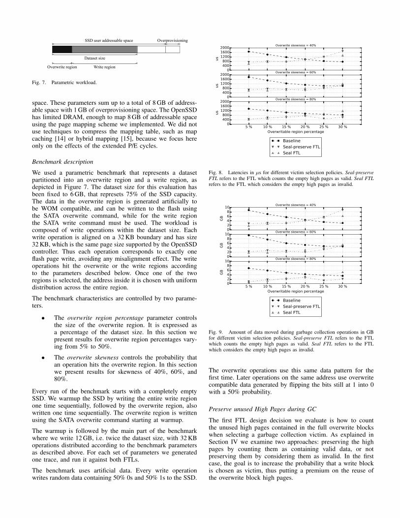
SSD user addressable space Overprovisioning
Overwrite region Write region
Dataset size
Fig. 7. Parametric workload.
space. These parameters sum up to a total of 8 GB of address-able space with 1 GB of overprovisioning space. The OpenSSDhas limited DRAM, enough to map 8 GB of addressable spaceusing the page mapping scheme we implemented. We did notuse techniques to compress the mapping table, such as mapcaching [14] or hybrid mapping [15], because we focus hereonly on the effects of the extended P/E cycles.
Benchmark description
We used a parametric benchmark that represents a datasetpartitioned into an overwrite region and a write region, asdepicted in Figure 7. The dataset size for this evaluation hasbeen fixed to 6 GB, that represets 75% of the SSD capacity.The data in the overwrite region is generated artificially tobe WOM compatible, and can be written to the flash usingthe SATA overwrite command, while for the write regionthe SATA write command must be used. The workload iscomposed of write operations within the dataset size. Eachwrite operation is aligned on a 32 KB boundary and has size32 KB, which is the same page size supported by the OpenSSDcontroller. Thus each operation corresponds to exactly oneflash page write, avoiding any misalignment effect. The writeoperations hit the overwrite or the write regions accordingto the parameters described below. Once one of the tworegions is selected, the address inside it is chosen with uniformdistribution across the entire region.
The benchmark characteristics are controlled by two parame-ters.
• The overwrite region percentage parameter controlsthe size of the overwrite region. It is expressed asa percentage of the dataset size. In this section wepresent results for overwrite region percentages vary-ing from 5% to 50%.
• The overwrite skewness controls the probability thatan operation hits the overwrite region. In this sectionwe present results for skewness of 40%, 60%, and80%.
Every run of the benchmark starts with a completely emptySSD. We warmup the SSD by writing the entire write regionone time sequentially, followed by the overwrite region, alsowritten one time sequentially. The overwrite region is writtenusing the SATA overwrite command starting at warmup.
The warmup is followed by the main part of the benchmarkwhere we write 12 GB, i.e. twice the dataset size, with 32 KBoperations distributed according to the benchmark parametersas described above. For each set of parameters we generatedone trace, and run it against both FTLs.
The benchmark uses artificial data. Every write operationwrites random data containing 50% 0s and 50% 1s to the SSD.
0400800
120016002000
us
Overwrite skewness = 40%
0400800
120016002000
us
Overwrite skewness = 60%
5 % 10 % 15 % 20 % 25 % 30 %Overwritable region percentage
0400800
120016002000
us
Overwrite skewness = 80%
Baseline
Seal-preserve FTL
Seal FTL
Fig. 8. Latencies in µs for different victim selection policies. Seal-preserveFTL refers to the FTL which counts the empty high pages as valid. Seal FTLrefers to the FTL which considers the empty high pages as invalid.
02468
10
GB
Overwrite skewness = 40%
02468
10
GB
Overwrite skewness = 60%
5 % 10 % 15 % 20 % 25 % 30 %Overwritable region percentage
02468
10
GB
Overwrite skewness = 80%
Baseline
Seal-preserve FTL
Seal FTL
Fig. 9. Amount of data moved during garbage collection operations in GBfor different victim selection policies. Seal-preserve FTL refers to the FTLwhich counts the empty high pages as valid. Seal FTL refers to the FTLwhich considers the empty high pages as invalid.
The overwrite operations use this same data pattern for thefirst time. Later operations on the same address use overwritecompatible data generated by flipping the bits still at 1 into 0with a 50% probability.
Preserve unused High Pages during GC
The first FTL design decision we evaluate is how to countthe unused high pages contained in the full overwrite blockswhen selecting a garbage collection victim. As explained inSection IV we examine two approaches: preserving the highpages by counting them as containing valid data, or notpreserving them by considering them as invalid. In the firstcase, the goal is to increase the probability that a write blockis chosen as victim, thus putting a premium on the reuse ofthe overwrite block high pages.

0400800
120016002000
us
Overwrite skewness = 40%
0400800
120016002000
us
Overwrite skewness = 60%
5 % 10 % 15 % 20 % 25 % 30 % 50 %Overwritable region percentage
0400800
120016002000
us
Overwrite skewness = 80%
Baseline
Seal FTL
Fig. 10. Average latency (µs) of all the write operations. This includes alsothe operations executed using the SATA overwrite command in the benchmarkrun on the extended P/E enabled SSD.
The graphs presented in Figure 8 and 9 show, respectively,the average latency per operation and the total amount of datamoved by garbage collections in three cases. The lines labeledas seal-preserve FTL refer to the FTL counting the empty highpages as containing valid data. The FTL which counts the highpages as invalid is simply labeled as seal FTL because it showsthe best behavior and is the one considered in the rest of theevaluation.
The first thing to observe is that both FTLs show the sametrend: they offer the biggest benefit, with respect to the baselineFTL, when the overwrite region percentage is low, and reducetheir performance with a growing overwrite region percentage.The seal FTL is better than the seal-preserve FTL, for all over-write skewness values, when the overwrite region percentage issmaller than 20%. Above that watermark the seal-preserve FTLhas better performance than the seal FTL for high overwriteskewness (significantly better for 80% overwrite skewness).However, when the overwrite percentage grows above 30%the performance of the seal-preserve FTL degrade so muchthat the OpenSSD becomes unresponsive causing the crash ofthe benchmark run. This is caused by the fact that when theoverwrite region percentage grows, the number of full writeblocks decreases, therefore they contain more valid pages. Atthis point the seal-preserve FTL does not seal the full overwriteblocks because considers all their pages as valid, and thereforetriggers garbage collections on full write blocks containingmany valid pages. Every garbage collection procedure cleansa few pages, and therefore the FTL has to invoke the garbagecollection every few operations, increasing the latency to thepoint where the device becomes unresponsive.
Our conclusion is that the seal-preserve FTL is very sensitiveto the parameters of the workload. It is the better choice for arestricted set of workload characteristics, i.e. between 20% and30% overwrite region percentage in our parametric workload,and overwrite skewness higher than 60%. It is possible to finetune the seal FTL to switch to the seal-preserve policy in thoseconditions, however in the rest of the evaluation we consideronly the seal FTL.
02468
10
GB
Overwrite skewness = 40%
02468
10
GB
Overwrite skewness = 60%
5 % 10 % 15 % 20 % 25 % 30 % 50 %Overwritable region percentage
02468
10
GB
Overwrite skewness = 80%
Baseline
Seal FTL
Fig. 11. Amount of data (GB) moved by garbage collection proceduresduring the entire benchmark run.
Performance
Figures 10 and 11 show the performance of the baseline FTLcompared to the seal FTL. The graphs show, respectively, theaverage write latency and the amount of data moved duringthe garbage collection operations. The results show that thelatency depends directly on the data copied during garbagecollection.
The first thing to notice in these graphs is that the trend of bothmetrics holds for different overwrite skewness values. Withhigher overwrite skewness the seal FTL exploits more pagereprograms on the low pages of the overwrite blocks.
However, the parameter that mostly affects performance is theoverwrite space percentage. When this percentage is low, theextended P/E cycles result in a great performance benefit.We measured the highest benefit with an overwrite spacepercentage of 5% and an overwrite skewness of 60%. In thoseconditions, the seal FTL exhibits a reduction of 67% in latencyand 80% in the amount of data copied during garbage collec-tion. With higher overwrite skewness, the extended P/E cyclestechnique is even more effective, but the benefit compared tothe baseline FTL is not as big.
When the overwrite space percentage increases, the perfor-mance of the seal FTL decrease rapidly. To explore the reasonsfor the performance drop we extracted and examined twoadditional metrics.
Distance between overwrite operations: Figure 12 shows thedistribution of the distances between two overwrite operationson the same location. The distances are measured as GBthat are written between the two operations. This metric isvery similar to the cache reuse distance used to evaluatecaching effectiveness. Ideally, when a page is written in anoverwrite block, the FTL should be able to allocate spaceequal to this distance in other blocks, before sealing it. Thisway the page can be reprogrammed. An important role inthis regard is played by the overprovisioning space and theportion of addressable space not occupied by the dataset. Inthis evaluation, the overprovisioning space is set to 1 GB,

0 1 2 3 4 5 6 7 8 9GB
0
1000
2000
3000
4000
5000
6000
7000
Ow space %: 5Ow space %: 10Ow space %: 15Ow space %: 20Ow space %: 25Ow space %: 30Ow space %: 50
Fig. 12. Distribution of the distance between overwrites on the same location.It is measured as the amount of data (GB) written between the two operations.This graph reports the values for overwrite skewness 80%.
5 % 10 % 15 % 20 % 25 % 30 % 50 %Percentage of overwritable space
30%
40%
50%
60%
70%
80%
90%
100%
ow skewness = 40ow skewness = 60ow skewness = 80
Fig. 13. Percentage of overwrite commands that are translated into flashreprogram operations.
while the unoccupied portion is 2 GB. The graph shows thatin the scenario with 5% overwrite space the distance is wellbelow the 3 GB watermark. When the distance approaches orsurpasses the watermark, the performance drops. This metricis extremely important for applications willing to exploit theextended P/E cycles. The access pattern must be analyzed toensure that the distance between overwrite operations presentsa favorable profile.
Page reprogram percentage: The second metric, plotted inFigure 13, is the percentage of overwrite operations that aresuccessfully translated by the FTL into page reprograms.Recall that not all the overwrite operations result in pagereprograms. For instance, when the overwrite blocks aresealed, the pages contained therein can not be reprogrammed.Another cause of missed reprogram is that after 8 consecutivereprogram operations to the same page, the page is reallocatedto a different overwrite block, to simulate the ECC limitations,
0123456
Overwrite skewness = 40%
0123456
# E
rase
ops
(10
00
)
Overwrite skewness = 60%
5 % 10 % 15 % 20 % 25 % 30 % 50 %Overwritable region percentage
0123456
Overwrite skewness = 80%
Baseline
Seal FTL
Fig. 14. Number of garbage collection operations, equivalent to the numberof erase operations.
as described in Section IV. This graph, according to theother metrics, shows that when the overwrite space percentageincreases it is more difficult for the FTL to reprogram pages.The overwrite operations are spread across a higher portionof the data set, and require more overwrite blocks. In turn,the accumulation of overwrite blocks reduces the number ofthe write blocks that will contain, in average, more valid data.As a consequence of this increase, more overwrite blocks areprematurely chosen as garbage collection victims, because theoverwrite blocks can have at maximum half the valid datacontained in the write blocks (only half pages are used beforesealing). When the write blocks have more than half validpages, the overwrite blocks are necessarily chosen as victims.
Endurance
Figure 14 shows the number of garbage collection operations.The results show the same trend observed in the performanceevaluation, therefore the same considerations discussed beforeapply here. Every garbage collection invocation correspondsto one block erase operation. The FTL does not perform eraseoperations in any other circumstance. Therefore, a reduction ingarbage collections causes a direct increase in endurance, sincethe erase operations are the major cause of wearout (as deducedfrom our BER analysis). We observed a garbage collectionreduction of 71% and 85% with overwrite skewness of 60%and 80%, respectively, when the overwrite space percentage is5%.
It is interesting to note that the stark reduction of the totalamount of data copied by garbage collection shown in Fig-ure 11 is caused only by the reduction of the number of garbagecollection operations, and not by a reduction of data moved byeach of them. Figure 15 shows the amount of data copied inaverage by single garbage collection operations. The baselineFTL shows a decreasing trend with a growing overwrite regionpercentage, while the seal FTL shows an increasing trendand exceeds the baseline FTL starting with overwrite regionpercentage of 10% for overwrite skewness of 80%. However,with the same overwrite skewness, the total amount of data

0.00.51.01.52.02.5
MB
Overwrite skewness = 40%
0.00.51.01.52.02.5
MB
Overwrite skewness = 60%
5 % 10 % 15 % 20 % 25 % 30 % 50 %Overwritable region percentage
0.00.51.01.52.02.5
MB
Overwrite skewness = 80%
Baseline
Seal FTL
Fig. 15. Average amount of data (MB) moved per garbage collection.
copied during garbage collection by the seal FTL meets andexceeds the baseline FTL only when the overwrite regionpercentage is greater than 25%. Between these two overwriteregion percentages the benefit of the seal FTL is obtained onlyfrom the sheer reduction of garbage collection invocations.Similar considerations apply to the other overwrite skewnessvalues.
Read performance
The read performance is not affected by the extended P/Ecycles, as they are implemented in this work, because thesize of the data is not modified by the FTL and there is noadditional step involved (e.g. no WOM encoding is performedwithin the FTL). Thus, the analysis presented here does notconsider read operations. However, if the application requiressome space overhead or additional steps to generate WOMcompatible data then the read and write performance may beaffected. The evaluation of such effects is out of the scope ofthis work.
VI. RELATED WORK
FTL development received considerable attention in academicliterature after the appearance of the first commercial SSDs.Our technique is orthogonal to the mapping technique andtherefore can be applied to most schemes [14], [15], [18],[19]. In our implementation we opted for a plain page-mappedscheme to avoid the effect of a particular FTL optimization onthe results.
The FTL we presented is designed to accept overwrite com-mands through the SATA interface. Therefore, it delegatesthe responsibility for generating WOM compatible data to theapplication. Other approaches have been proposed: Odeh at al.and Yadgar et al. presented designs where the FTL internallyuses WOM codes to perform reprogram operations, referredto as second writes [4], [7].
Applications using WOM codes [2], [5] can directly useour FTL implementation. However, as shown by our exper-iments, the highest benefit is obtained when overwrites are
concentrated in a small portion of the dataset. Therefore, it isadvisable to use WOM codes on a restricted and frequentlyupdated subsection of it, as in [4], [7].
The reprogram operation was discussed by Jagmohan et al.,Kaiser et al., Odeh et al, and Yadgar et al. in [2]–[4], [7].However, those studies are based on simulations and do notattempt to implement the operation on a real prototype. To thebest of our knowledge this work is the first attempt at doing so.Furthermore Jagmohan et al. discuss the reprogram operation,referred to as eraseless program, only in SLC flash chips.
The diagram presented in Figure 3 is consistent with thefindings of Grupp et al. presented in [6]. Their experimentsconsisted of erasing a block and repeatedly programming halfof one page to 0. They present two results, which can beexplained by the transitions outlined in our diagram:
• reprogramming the low pages does not disturb otherpages. This case corresponds to one first use oftransition 1, and then repeated uses of transition 3 withthe intent to program the low bit to 0. Both transitionsare safe, and therefore no error was detected.
• reprogramming the high page disturbs the bits of thecorresponding low page after two reprograms. Thiscase corresponds to one first use of transition 2, thatis safe, and then one use of transition 7 which isunsafe because it causes program disturb on the lowbit. Therefore, the errors detected are in line with ourstate diagram.
Kaiser et al. present a B-Tree that uses unsorted nodes andappend new key-value pairs in the node. This approach allowsto write the nodes with the SATA overwrite command, becauseappending is by definition WOM compatible. This B-Treecould directly be stored on a SSD with the seal FTL. In theoriginal publication the authors considered a simplified modelwhere every flash page could be reprogrammed.
VII. CONCLUSION
In this work we presented the extended P/E cycles techniqueimplemented through page reprograms. This technique cancause a loss of capacity in MLC flash since only the lowpages of a block can be used for reprograms. We showed howto circumvent this drawback through overwrite block sealing.This technique enables the utilization of the complete capacityof blocks whose pages were previously reprogrammed.
During the development of the overwrite block sealing, weextracted the state transition diagram for MLC flash. So far,not all the transitions in the diagram are used. However, thediagram can be the foundation for data encoding researchaimed at utilizing all the transitions and increase the MLCutilization.
The BER analysis we performed showed that the erase voltageis the major contributor to flash cell wear. Extended P/E cycleshave the same number of erase operations as normal P/Ecycles, but can write more data per cycle, therefore increasingthe lifetime of flash cells. Our evaluation shows that thistechnique can reduce erase operations by as much as 85%on workloads with certain characteristics. Furthermore, whenused in optimal conditions, it can lead to latency reduction as
high as 67% with up to 60% less data copied internally by theFTL.
The technique presented here is not directly applicable to everyapplication. First, the data must be WOM compatible, and thisrequires some special data structure design, or encoding partof the dataset with WOM codes. Second, the access patternmust exhibit some specific properties, detailed in Section V.However, we believe that the benefits are such that designersseeking to squeeze the best performance and lifetime fromflash devices should consider this technique and the insightspresented here.
The source code for the FTLs presented in this paper isavailable at https://github.com/zdvresearch.
VIII. ACKNOWLEDGEMENT
We would like to thank our shepherd Gala Yadgar for herguidance and support, and the anonymous reviewers for theirinsightful comments.
REFERENCES
[1] L. M. Grupp, J. D. Davis, and S. Swanson, “The bleak future of NANDflash memory,” in Proceedings of the 10th USENIX conference on Fileand Storage Technologies, FAST 2012, San Jose, CA, USA, February14-17, 2012, p. 2.
[2] A. Jagmohan, M. Franceschini, and L. Lastras, “Write amplificationreduction in NAND flash through multi-write coding,” in Proceedingsof the 26th IEEE Conference on Mass Storage Systems and Technologies(MSST), 2010, pp. 1–6.
[3] J. Kaiser, F. Margaglia, and A. Brinkmann, “Extending SSD lifetimein database applications with page overwrites,” in Proceedings of the6th Annual International Systems and Storage Conference (SYSTOR),2013, p. 11.
[4] G. Yadgar, E. Yaakobi, and A. Schuster, “Write once, get 50% free:Saving SSD erase costs using WOM codes,” in Proceedings of the 13thUSENIX Conference on File and Storage Technologies (FAST), 2015.
[5] R. L. Rivest and A. Shamir, “How to reuse a ”write-once” memory,”Information and Control, vol. 55, no. 1-3, pp. 1–19, 1982.
[6] L. M. Grupp, A. M. Caulfield, J. Coburn, S. Swanson, E. Yaakobi,P. H. Siegel, and J. K. Wolf, “Characterizing flash memory: anomalies,observations, and applications,” in Proceedings of the 42st AnnualIEEE/ACM International Symposium on Microarchitecture (MICRO),2009, pp. 24–33.
[7] S. Odeh and Y. Cassuto, “NAND flash architectures reducing writeamplification through multi-write codes,” in Proceedings of the 30thIEEE Conference on Mass Storage Systems and Technologies (MSST),2014.
[8] The OpenSSD Project, “Indilinx Jasmine platform,” www.openssd-project.org.
[9] W. Bux and I. Iliadis, “Performance of greedy garbage collection inflash-based solid-state drives,” Performance Evaluation, vol. 67, no. 11,pp. 1172–1186, 2010.
[10] J. Hsieh, T. Kuo, and L. Chang, “Efficient identification of hot data forflash memory storage systems,” ACM Transactions on Storage (TOS),vol. 2, no. 1, pp. 22–40, 2006.
[11] B. Bloom, “Space/time trade-offs in hash coding with allowable errors,”Communications of the ACM, vol. 13, no. 7, pp. 422–426, 1970.
[12] E. Yaakobi, J. Ma, L. Grupp, P. H. Siegel, S. Swanson, and J. K.Wolf, “Error characterization and coding schemes for flash memories.”in GLOBECOM Workshops (GC Wkshps), IEEE, 2010, pp. 1859–1860.
[13] S.-W. Lee, D.-J. Park, T.-S. Chung, D.-H. Lee, S. Park, and H.-J. Song,“A log buffer-based flash translation layer using fully-associative sectortranslation,” ACM Trans. Embed. Comput. Syst., vol. 6, no. 3, Jul. 2007.
[14] A. Gupta, Y. Kim, and B. Urgaonkar, “DFTL: a flash translationlayer employing demand-based selective caching of page-level addressmappings,” in Proceedings of the 14th International Conference onArchitectural Support for Programming Languages and Operating Sys-tems, ASPLOS 2009, Washington, DC, USA, March 7-11, 2009, pp.229–240.
[15] S.-P. Lim, S.-W. Lee, and B. Moon, “FASTer FTL for enterprise-classflash memory SSDs,” in Proceedings of the 6th IEEE InternationalWorkshop on Storage Network Architecture and Parallel I/Os (SNAPI),2010, pp. 3–12.
[16] E. E. Gad, Y. Li, J. Kliewer, M. Langberg, A. Jiang, and J. Bruck,“Polar coding for noisy write-once memories,” Proceedings of IEEEInternational Symposium on Information Theory (ISIT), 2014.
[17] X. Jimenez, D. Novo, and P. Ienne, “Wear unleveling: improving NANDflash lifetime by balancing page endurance,” in Proceedings of the 12thUSENIX conference on File and Storage Technologies, FAST 2014,Santa Clara, CA, USA, February 17-20, 2014, 2014, pp. 47–59.
[18] S. Lee, D. Park, T. Chung, D. Lee, S. Park, and H. Song, “A log buffer-based flash translation layer using fully-associative sector translation,”ACM Transactions in Embedded Computing Systems, vol. 6, no. 3, 2007.
[19] F. Chen, T. Luo, and X. Zhang, “CAFTL: A content-aware flashtranslation layer enhancing the lifespan of flash memory based solidstate drives.” Proceedings of the USENIX Conference on File andStorage Technologies (FAST), vol. 11, 2011.