improving high resolution tem images using low energy ion ... improving high resolution tem... ·...
TRANSCRIPT
EM Sample Preparation
Introduction
Ion beam milling has become a widespread specimen preparation technique for non-biological materials over the last two decades, particularly for cross-sectional and plan-view transmission electron microscope (TEM) specimens. The basic principle of ion milling involves bombarding a specimen with energetic ions or neutral atoms acclerated and formed into a tightly focused ion beam. Material is sputtered from the specimen resulting in electron transparent areas around the area of interest. Geometrical arrangements from system to system vary, but typically the specimen is rotated or oscillated relative to the ion beam during the milling process. The ion beam is tilted at a given angle with respect to the specimen surface during the ion beam milling process and is adjusted from 0 to 15 degrees.
The disadvantage of ion beam milling specimens for TEM are the artifacts produced during the process. Artifacts include preferential sputtering (one material sputtering at a different rate than another), specimen heating, and radiation damage. Minimizing the incident ion angle to the surface of the sample has been found to be one of the most effective techniques for reducing these effects on the specimen. However, the major artifact that still remains directly resulting from ion milling is the amorphous damage created due to high energy ion bombardment. It has been well known that this process of ion bombardment (typically from 2 – 10 keV) causes damage in the crystalline structure (Ishiguro, et al, 1987). In the case of semiconductor crystals (such as Si and GaAs), this damage appears mostly as amorphous material on the surfaces of the thinned sample. Reducing the incident ion energy used during the milling process has been found to dramatically reduce and eliminate the amorphous damage produced by traditional ion milling techniques (G. Radnoczi, A. Barna, 1996).
The GentleMill™
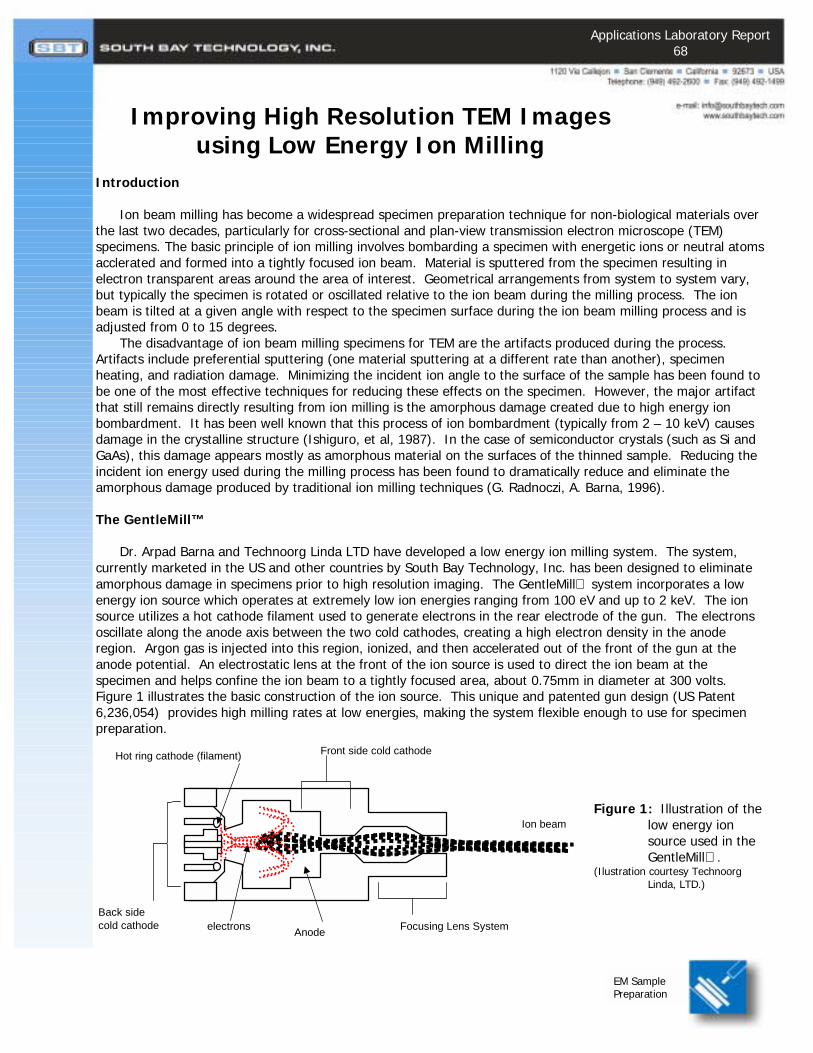
Dr. Arpad Barna and Technoorg Linda LTD have developed a low energy ion milling system. The system, currently marketed in the US and other countries by South Bay Technology, Inc. has been designed to eliminate amorphous damage in specimens prior to high resolution imaging. The GentleMill system incorporates a low energy ion source which operates at extremely low ion energies ranging from 100 eV and up to 2 keV. The ion source utilizes a hot cathode filament used to generate electrons in the rear electrode of the gun. The electrons oscillate along the anode axis between the two cold cathodes, creating a high electron density in the anode region. Argon gas is injected into this region, ionized, and then accelerated out of the front of the gun at the anode potential. An electrostatic lens at the front of the ion source is used to direct the ion beam at the specimen and helps confine the ion beam to a tightly focused area, about 0.75mm in diameter at 300 volts. Figure 1 illustrates the basic construction of the ion source. This unique and patented gun design (US Patent 6,236,054) provides high milling rates at low energies, making the system flexible enough to use for specimen preparation.
Figure 1: Illustration of the
low energy ion source used in the GentleMill .
(Ilustration courtesy Technoorg Linda, LTD.)
Applications Laboratory Report 68
Improving High Resolution TEM Images using Low Energy Ion Milling
Back side cold cathode Focusing Lens System
Front side cold cathode
Anode
Hot ring cathode (filament)
Ion beam
electrons
EM Sample Preparation
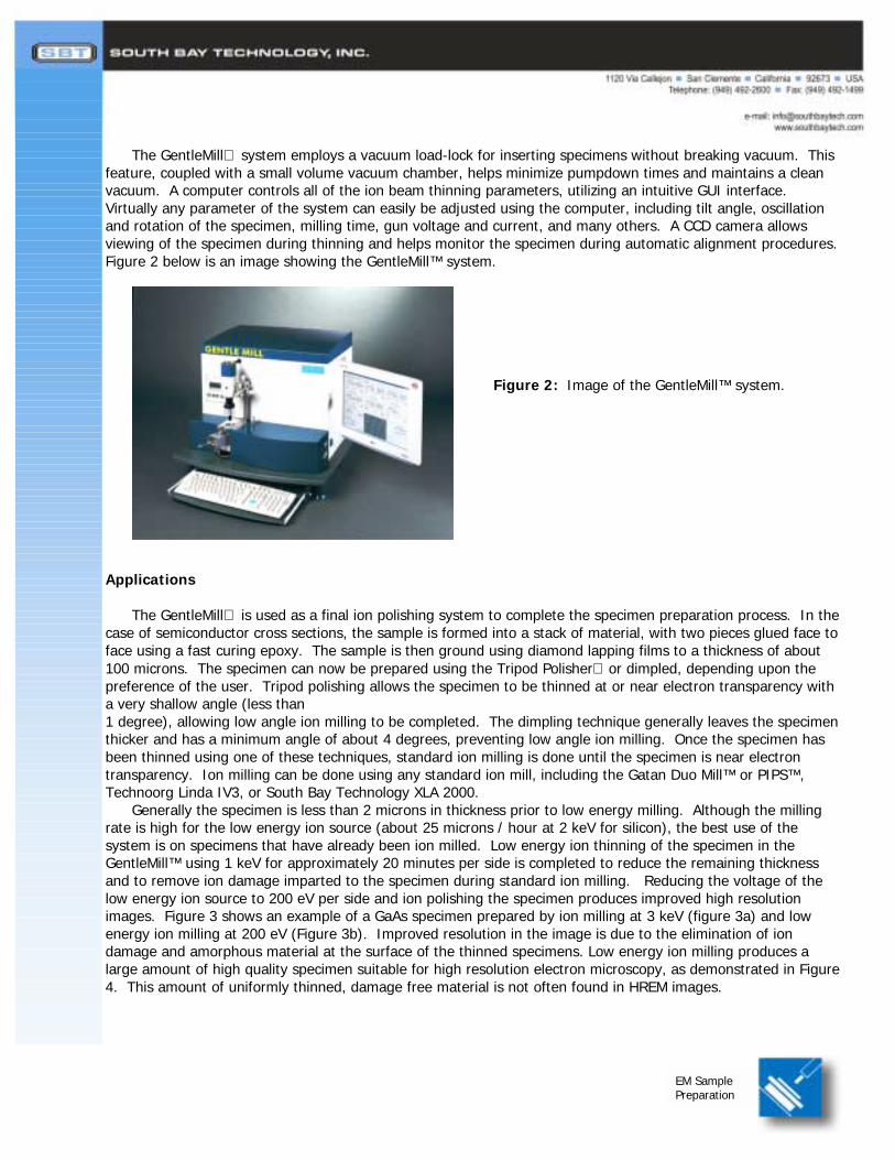
The GentleMill system employs a vacuum load-lock for inserting specimens without breaking vacuum. This
feature, coupled with a small volume vacuum chamber, helps minimize pumpdown times and maintains a clean vacuum. A computer controls all of the ion beam thinning parameters, utilizing an intuitive GUI interface. Virtually any parameter of the system can easily be adjusted using the computer, including tilt angle, oscillation and rotation of the specimen, milling time, gun voltage and current, and many others. A CCD camera allows viewing of the specimen during thinning and helps monitor the specimen during automatic alignment procedures. Figure 2 below is an image showing the GentleMill™ system.
Figure 2: Image of the GentleMill™ system.
Applications
The GentleMill is used as a final ion polishing system to complete the specimen preparation process. In the case of semiconductor cross sections, the sample is formed into a stack of material, with two pieces glued face to face using a fast curing epoxy. The sample is then ground using diamond lapping films to a thickness of about 100 microns. The specimen can now be prepared using the Tripod Polisher or dimpled, depending upon the preference of the user. Tripod polishing allows the specimen to be thinned at or near electron transparency with a very shallow angle (less than 1 degree), allowing low angle ion milling to be completed. The dimpling technique generally leaves the specimen thicker and has a minimum angle of about 4 degrees, preventing low angle ion milling. Once the specimen has been thinned using one of these techniques, standard ion milling is done until the specimen is near electron transparency. Ion milling can be done using any standard ion mill, including the Gatan Duo Mill™ or PIPS™, Technoorg Linda IV3, or South Bay Technology XLA 2000.
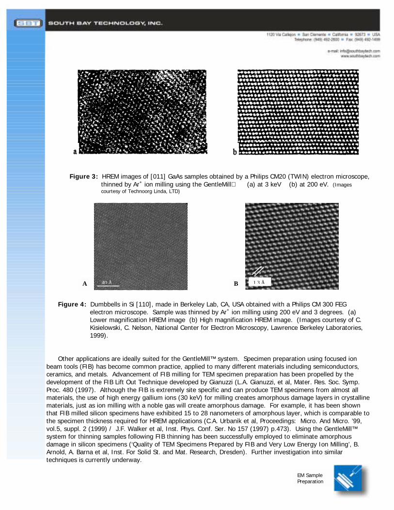
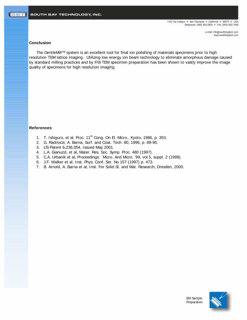
Generally the specimen is less than 2 microns in thickness prior to low energy milling. Although the milling rate is high for the low energy ion source (about 25 microns / hour at 2 keV for silicon), the best use of the system is on specimens that have already been ion milled. Low energy ion thinning of the specimen in the GentleMill™ using 1 keV for approximately 20 minutes per side is completed to reduce the remaining thickness and to remove ion damage imparted to the specimen during standard ion milling. Reducing the voltage of the low energy ion source to 200 eV per side and ion polishing the specimen produces improved high resolution images. Figure 3 shows an example of a GaAs specimen prepared by ion milling at 3 keV (figure 3a) and low energy ion milling at 200 eV (Figure 3b). Improved resolution in the image is due to the elimination of ion damage and amorphous material at the surface of the thinned specimens. Low energy ion milling produces a large amount of high quality specimen suitable for high resolution electron microscopy, as demonstrated in Figure 4. This amount of uniformly thinned, damage free material is not often found in HREM images.
EM Sample Preparation
Figure 3: HREM images of [011] GaAs samples obtained by a Philips CM20 (TWIN) electron microscope, thinned by Ar+ ion milling using the GentleMill (a) at 3 keV (b) at 200 eV. (Images courtesy of Technoorg Linda, LTD)
Figure 4: Dumbbells in Si [110], made in Berkeley Lab, CA, USA obtained with a Philips CM 300 FEG
electron microscope. Sample was thinned by Ar+ ion milling using 200 eV and 3 degrees. (a) Lower magnification HREM image (b) High magnification HREM image. (Images courtesy of C. Kisielowski, C. Nelson, National Center for Electron Microscopy, Lawrence Berkeley Laboratories, 1999).
Other applications are ideally suited for the GentleMill™ system. Specimen preparation using focused ion beam tools (FIB) has become common practice, applied to many different materials including semiconductors, ceramics, and metals. Advancement of FIB milling for TEM specimen preparation has been propelled by the development of the FIB Lift Out Technique developed by Gianuzzi (L.A. Gianuzzi, et al, Mater. Res. Soc. Symp. Proc. 480 (1997). Although the FIB is extremely site specific and can produce TEM specimens from almost all materials, the use of high energy gallium ions (30 keV) for milling creates amorphous damage layers in crystalline materials, just as ion milling with a noble gas will create amorphous damage. For example, it has been shown that FIB milled silicon specimens have exhibited 15 to 28 nanometers of amorphous layer, which is comparable to the specimen thickness required for HREM applications (C.A. Urbanik et al, Proceedings: Micro. And Micro. ’99, vol.5, suppl. 2 (1999) / J.F. Walker et al, Inst. Phys. Conf. Ser. No 157 (1997) p.473). Using the GentleMill™ system for thinning samples following FIB thinning has been successfully employed to eliminate amorphous damage in silicon specimens (‘Quality of TEM Specimens Prepared by FIB and Very Low Energy Ion Milling’, B. Arnold, A. Barna et al, Inst. For Solid St. and Mat. Research, Dresden). Further investigation into similar techniques is currently underway.
40 Å
1 3 ÅA B
EM Sample Preparation
Conclusion
The GentleMill™ system is an excellent tool for final ion polishing of materials specimens prior to high resolution TEM lattice imaging. Utilizing low energy ion beam technology to eliminate amorphous damage caused by standard milling practices and by FIB TEM specimen preparation has been shown to vastly improve the image quality of specimens for high resolution imaging.
References
1. T. Ishiguro, et al, Proc. 11th Cong. On El. Micro., Kyoto, 1986, p. 353. 2. G. Radnoczi, A. Barna, Surf. and Coat. Tech. 80, 1996, p. 89-95. 3. US Patent 6,236,054, Issued May 2001. 4. L.A. Gianuzzi, et al, Mater. Res. Soc. Symp. Proc. 480 (1997). 5. C.A. Urbanik et al, Proceedings: Micro. And Micro. ’99, vol.5, suppl. 2 (1999). 6. J.F. Walker et al, Inst. Phys. Conf. Ser. No 157 (1997) p. 473. 7. B. Arnold, A. Barna et al, Inst. For Solid St. and Mat. Research, Dresden, 2000.