improvement of noise performance in phased-array …hompi.sogang.ac.kr/rfdesign/paper/22.pdf ·...
TRANSCRIPT

176 Junghyun Kim et al. © 2011 ETRI Journal, Volume 33, Number 2, April 2011
This paper presents a new analytical approach and experimental verification for the improvement of noise performance in phased-array receivers. For analysis purposes, a multi-channel array system is converted into an equivalent single-channel system, such that the two presents the identical signal and noise powers at the output, respectively. We define an effective gain, noise figure, and signal-to-noise ratio in the equivalent system. Through the proposed approach, the noise performance of the array receiver is analyzed in a general and straightforward manner and then compared to that of each individual array channel. In addition, the phase noise of the array system is analyzed in a rigorous manner, showing its effective reduction by a factor of the array size. The predicted improvement of the noise performance is experimentally confirmed with a CMOS integrated phased-array receiver.
Keywords: CMOS, noise figure, phased-array receiver, phase noise, RFIC, signal-to-noise ratio.
Manuscript received July 22, 2010, revised Sept. 27, 2010; accepted Oct. 25, 2010. This work was supported by Basic Science Research Program through the National
Research Foundation of Korea (NRF) funded by the Ministry of Education, Science and Technology (2010-0015278).
Junghyun Kim (phone: +82 31 400 5233, email: [email protected]) is with the School of Electrical Engineering and Computer Science, Hanyang University, Ansan, Rep. of Korea.
Jinho Jeong (email: [email protected]) is with the Department of Electronic Engineering, Sogang University, Seoul, Rep. of Korea.
Sanggeun Jeon (corresponding author, email: [email protected]) is with the School of Electrical Engineering, Korea University, Seoul, Rep. of Korea.
doi:10.4218/etrij.11.0110.0440
I. Introduction
Phased-array receivers are widely used in radars, radio astronomy, and wireless communications due to several benefits. In addition to the beam-steering capability, one well-known advantage over individual single-channel1) receivers is that the phased-array receivers improve noise performance, thereby enhancing receiver sensitivity [1]-[4]. This enables the receiver to detect or demodulate a weak incoming signal with minimal errors in a noisy environment.
Recently, as silicon device technology progresses, all or most of the building blocks for a phased array are integrated on a single silicon chip, reducing the system cost dramatically [4]-[6]. However, the radio frequency (RF) front-end blocks on silicon generally present higher noise than their traditional compound-semiconductor counterparts and thus impose a tight noise budget on the system configuration. Therefore, the improvement of the noise performance in array receivers is essential in the silicon integrated systems to relieve the noise budget of each RF block.
The noise performance improvement has been implied or tacitly utilized in several previous works on silicon integrated arrays [6]-[9]. Nonetheless, some noise characteristics of the phased-array receivers are ambiguously described, analyzed, and applied in different ways. For instance, it is implied in [7] that the noise figure of the array system improves with the number of array channels, while other studies claim that it is unchanged in the array system [8], [9]. Apparently, the claim that the system noise figure is unchanged seems to contradict the widely-accepted fact that the sensitivity of array receivers
1) Throughout the paper, a channel is defined as a single RF front-end chain in phased-array receivers.
Improvement of Noise Performance in Phased-Array Receivers
Junghyun Kim, Jinho Jeong, and Sanggeun Jeon

ETRI Journal, Volume 33, Number 2, April 2011 Junghyun Kim et al. 177
improves with the array size.2) This ambiguity arises because the noise figure and the associated gain are conventionally defined for a two-port system, so they cannot be clearly applied to a multiport system like a phased array.
To overcome this difficulty, we convert a multiport array receiver into an effective two-port system for the purpose of noise analysis. The effective system is equivalent to the original array in that the two produce identical signal and noise powers at the output under the same input environment (incoming power density and noise). In the effective two-port system, we are able to clearly define an effective gain, noise figure, and signal-to-noise ratio (SNR) as is conventionally done. The noise performance of the array receiver is analyzed with these effective parameters, avoiding the aforementioned ambiguity. This approach not only clarifies the noise performance improvement in array receivers but also provides a straightforward metric that compares the noise performance between different array receivers.
In order to reduce the system cost and complexity, the phased-array chips in silicon tend to integrate more RF building blocks on chip, even including a frequency generation block [7]-[9]. Unfortunately, the on-chip local oscillator (LO) source suffers from higher phase noise than its off-chip counterpart, thereby degrading the array performance. In this paper, we analyze the phase noise of the array in terms of the different noise contributions from each array channel. Similar to the noise properties found in coupled oscillators [10], we prove that the phase noise is significantly reduced at the array output when separate LO signals feed the array channels before the channel signals are combined. This phase noise improvement allows for the use of on-chip frequency generators without severe degradation of array performance. The results of the noise analysis are experimentally confirmed by measurements with a CMOS four-channel phased-array receiver. To the authors’ best knowledge, this includes the first experimental verification of phase noise improvement in an integrated phased-array receiver.
This paper is organized as follows. Section II presents an effective two-port analysis of phased-array receivers. In section III, we discuss the noise performance improvement in array systems through the effective two-port equivalent. Section IV describes the phase noise improvement in the array systems. The experimental results are presented in section V. Section VI concludes this paper.
II. Effective Two-Port Analysis of Phased-Array Receivers
The general configuration of a phased-array receiver with a
2) The array size is defined as the number of channels in phased-array receivers.
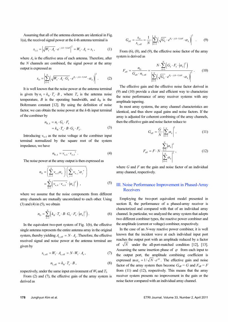
Fig. 1. (a) General configuration of a phased-array receiver with an array size of N and (b) two-port equivalent system of that in (a).
Combiner
Array outputsO, nO
Array inputWI, TI
Ae
Ae
Ae
sI,1, nI
sI,2, nI
sI,N, nI
G1, F1, θ1
G2, F2, θ2
GN, FN, θN
a1
a2
aN
nR,1
nR,2
nR,N
Array input WI, TI
Array output sO, nO
Ae, effsI, eff, nI, eff, Geff, Feff, θeff
(a)
(b)
size N is shown in Fig. 1(a). An incoming signal is received by the array of N antennas with a phase delay ∆θ between any two adjacent antennas. Each received signal is then processed independently by a subsequent individual array channel. The array channel basically adjusts the amplitude and phase of the received signal, and may also contain down-conversion blocks, depending on the phase-shifting architecture [11]. For the purpose of analysis, the k-th array channel is characterized by a power gain Gk, an insertion phase shift θk, and a noise factor3) Fk at the operating frequency, where1 k N≤ ≤ . The multiple array channels are combined by an N-way combiner. The combiner, whether it combines power or an amplitude such as a voltage or current, is characterized by the amplitude combining coefficient ak from the k-th input to the output port. In general, the combining coefficient reflects the weighted amplitude tapering in the beamforming network.
It should be noted that the original phased-array receiver contains N input ports and a single output port. As mentioned before, this multiport property leads to an ambiguity in the noise analysis of the array system. The objective of this section is to reduce the original system to its two-port equivalent as shown in Fig. 1(b) to obtain a straightforward analysis. The effective power gain Geff and effective noise factor Feff are determined in terms of the original system parameters, such that the two systems generate identical signal and noise power levels at the output (sO and nO, respectively) under the same input environment (incident power density WI and background noise TI).
3) A noise factor (F) is a linearly-scaled version of a noise figure (NF) that is conventionally
expressed in dB, that is, NF = 10 log F (dB).
178 Junghyun Kim et al. ETRI Journal, Volume 33, Number 2, April 2011
Assuming that all of the antenna elements are identical in Fig. 1(a), the received signal power at the k-th antenna terminal is
2( 1)I, I e I e I
j kks W A e W A sθ− − Δ = ⋅ ⋅ = ⋅ = , (1)
where Ae is the effective area of each antenna. Therefore, after the N channels are combined, the signal power at the array output is expressed as
( )2
( 1)O I e
1
k
Nj k
k kk
s W A G eθ θ α− − Δ
=
= ⋅ ⋅ ⋅ ⋅∑ . (2)
It is well known that the noise power at the antenna terminal is given by I B an k T B= ⋅ ⋅ , where Ta is the antenna noise temperature, B is the operating bandwidth, and kB is the Boltzmann constant [12]. By using the definition of noise factor, we can obtain the noise power at the k-th input terminal of the combiner by
R, I
B .k k k
a k k
n n G Fk T B G F
= ⋅ ⋅
= ⋅ ⋅ ⋅ ⋅ (3)
Introducing vn, k as the noise voltage at the combiner input terminal normalized by the square root of the system impedance, we have
R, , ,k n k n kn v v ∗ = ⋅ . (4)
The noise power at the array output is then expressed as
( )O , ,
1 1
2, ,
1
,
N N
n k k n j jk j
N
n k n k kk
n v v
v v
α α
α
∗ ∗
= =
∗
=
⎛ ⎞⎛ ⎞= ⋅⎜ ⎟⎜ ⎟
⎝ ⎠ ⎝ ⎠
= ⋅ ⋅
∑ ∑
∑
(5)
where we assume that the noise components from different array channels are mutually uncorrelated to each other. Using (3) and (4) in (5), we obtain
( )2O B
1
N
a k k kk
n k T B G F α=
= ⋅ ⋅ ⋅ ⋅ ⋅∑ . (6)
In the equivalent two-port system of Fig. 1(b), the effective single antenna represents the entire antenna array in the original system, thereby yielding e, eff e .A N A = ⋅ Therefore, the effective received signal and noise power at the antenna terminal are given by
I, eff I e, eff I es W A N W A = ⋅ = ⋅ ⋅ , (7)
I, eff B an k T B = ⋅ ⋅ , (8)
respectively, under the same input environment of WI and TI. From (2) and (7), the effective gain of the array system is
derived as
( )2
( 1)Oeff
1I, eff
1k
Nj k
k kk
sG G e
s Nθ θ α− − Δ
=
= = ⋅ ⋅ ⋅∑ . (9)
From (6), (8), and (9), the effective noise factor of the array system is derived as
( )
( )
2
O 1eff 2
eff I, eff ( 1)
1
k
N
k k kk
Nj k
k kk
N G Fn
FG n
G eθ θ
α
α
=
− − Δ
=
⋅ ⋅ ⋅= =
⋅⋅ ⋅
∑
∑. (10)
The effective gain and the effective noise factor derived in (9) and (10) provide a clear and efficient way to characterize the noise performance of array receiver systems with any amplitude tapering.
In most array systems, the array channel characteristics are identical, and thus show equal gains and noise factors. If the array is adjusted for coherent combining of the array channels, then the effective gain and noise factor reduce to
2
eff1
N
kk
GGN
α=
= ⋅ ∑ , (11)
2
1eff 2
1
N
kk
N
kk
F F Nα
α
=
=
= ⋅ ⋅∑
∑, (12)
where G and F are the gain and noise factor of an individual array channel, respectively.
III. Noise Performance Improvement in Phased-Array Receivers
Employing the two-port equivalent model presented in section II, the performance of a phased-array receiver is characterized and compared with that of an individual array channel. In particular, we analyzed the array system that adopts two different combiner types, the reactive power combiner and the amplitude (current or voltage) combiner, respectively.
In the case of an N-way reactive power combiner, it is well known that the incident wave at each individual input port reaches the output port with an amplitude reduced by a factor of N under the all-port-matched condition [12], [13]. Assuming the same insertion phase of ϕ from each input to the output port, the amplitude combining coefficient is expressed as 1/ j
k N e ϕα = ⋅ . The effective gain and noise factor of the array system then become Geff = G and Feff = F from (11) and (12), respectively. This means that the array receiver system presents no improvement in the gain or the noise factor compared with an individual array channel.

ETRI Journal, Volume 33, Number 2, April 2011 Junghyun Kim et al. 179
Table 1. Performance improvement in phased-array receiversemploying power or amplitude combiners. (G, F, and (S/N)O are the gain, noise factor, and output signal-to-noise ratio of an individual array channel, respectively. Nis the array size.)
Effective performance of array receiver
Power combiner employed
Amplitude combiner employed
Geff G N·G
Feff F F
(S/N)O, eff N·(S/N)O N·(S/N)O
On the other hand, when an N-way amplitude combiner is
adopted in the array system, the amplitude combining coefficient is given by j
k e ϕα = . Similarly, the effective gain and noise factor are obtained as effG N G= ⋅ and Feff = F. The power gain of the array system increases by a factor of N, as expected because the current (or voltage) out of each array channel is combined coherently. However, the noise factor remains unchanged.
Whether it adopts a power combiner or an amplitude combiner, a phased-array receiver does not improve the noise factor (or noise figure) from an individual array channel, but shows the same noise factor (or noise figure). This appears to contradict the widely accepted benefit of array systems that the array receiver sensitivity improves with the array size N. However, this is not the case; the output SNR increases in the array system. The output SNR is calculated from Fig. 1 as
I, eff IO, eff O
I, eff eff I
1 1s sSNR N N SNR
n F n F
= ⋅ = ⋅ ⋅ = ⋅ , (13)
where SNRO is the output SNR of an individual array channel. Although the noise figure remains unchanged, the output SNR increases by a factor of N in the array receiver, thus improving the receiver sensitivity. This result is not surprising because the array receiver collects an N-fold signal power, thus showing an N-times greater SNR at both the input and the output. The performance improvement in the array system compared with that in an individual channel is summarized in Table 1.
The output SNR improvement in a phased-array receiver reduces the error vector magnitude (EVM) and the bit error rate (BER) in the digital modulation schemes. When EVM is normalized to the square root of the average symbol power, it is related to the SNR [14] as
1 100%EVMSNR
≈ × , (14)
where the EVM is expressed in %rms. Therefore, as the output
Fig. 2. Simulated improvement of digital demodulation performance with array size. A 32-QAM signal with uncorrelated AWGN is assumed.
Array size 1 10 100
1
10–3
10–6
10–9
10–120
5
10
15
20
25
30
35
40SNR EVM BER
SNR
(dB
), EV
M (%
rms)
BER
SNR increases by a factor of N, the EVM reduces by N , thus leading to more reliable demodulation performance. In Fig. 2, the output SNR, EVM, and BER are calculated for a 32-QAM modulation scheme as the array size increases. The symbol SNR of a single-channel receiver, corresponding to N=1, is set to 12 dB with an additive white Gaussian noise applied. The noise is assumed to be mutually uncorrelated between the array channels while the signal is combined coherently. As shown in Fig. 2, the demodulation performance improves dramatically with the array size, which is a significant benefit of using array receivers.
IV. Phase Noise in Phased-Array Receivers
Advanced silicon technology enables high-level on-chip integration of the RF building blocks used for phased-array systems. The LO generators that include the VCO and PLL are also integrated on chip for cost and complexity reduction. However, the on-chip LO generators suffer from relatively high phase noise, thereby degrading aspects of the array performance such as beam-pointing accuracy. Fortunately, the poor phase noise may be improved significantly in the array receiver system where an individual LO source is employed in each array channel.
While the phase shifting is usually performed at the RF path in conventional array receivers, it may also be done effectively in the LO or the IF paths [11]. In the LO phase-shifting architecture in particular, each array channel is fed by an individual LO signal, the phase of which is adjusted independently. The LO signal is generated by either a common LO source or an individual source belonging to each array channel, as shown in Fig. 3.
After the down-conversion by a mixer, the k-th channel signal at the combiner input can be expressed as
( )0cos ,k k k kA A tω θ δθ= + + where ω0 is the carrier

180 Junghyun Kim et al. ETRI Journal, Volume 33, Number 2, April 2011
frequency, θk is the nominal phase, and kδθ is the phase fluctuation. The phase fluctuation can be decomposed into two different components depending on their origins. One originates from the noise sources that are mutually correlated between the array channels, that is, the phase noise contained in the common reference signal or the incoming RF signal. The other is from the uncorrelated noise sources, for example, the 1/f noise up-conversion by the nonlinear blocks belonging to each array channel. Denoting the two fluctuation components by ,c kδθ and , ,u kδθ respectively, and assuming a linear relationship between the phase fluctuation and the total phase,
, , .k c k u kδθ δθ δθ = + The array output signal after the combiner is then given by
( )out 0 , ,1
cosN
k k k k c k u kk
A A tα ω θ α δθ δθ =
= ⋅ + + + +∑ . (15)
When the array is adjusted for beamforming in a certain direction, the amplitude and the nominal phase of the array channels are uniformly aligned as
k kA Aα α⋅ = ⋅ , k kθ α θ α+ = + . (16)
Using (16) and the assumption that ,c kδθ and ,u kδθ are very small in (15), the array output signal reduces to
( )out 0 outcosA A N tα ω θ α δθ= ⋅ ⋅ + + + , (17)
where outδθ is the output phase fluctuation given by
( )out , ,1
1 N
c k u kkN
δθ δθ δθ =
= +∑ . (18)
The power spectrum of the phase fluctuation is then derived
Fig. 3. LO phase-shifting architecture for phased-array receivers.
Combiner
A1
φ
φ
φ
Array output
Phase shifter Frequency synthesizer Reference
source
A2
AN
Aout
a1
a2
aN
by applying the Wiener-Khinchin theorem for an ergodic process [15] to (18),
( ) ( )2 * *out , , , ,2
1 1
2 *, , ,2
1 1 1
1
1 ,
N N
c k u k c j u jk j
N N N
u k c k c jk k j
N
N
δ δ δ δ δ
δ δ δ
= =
= = =
Θ = Θ + Θ ⋅ Θ + Θ
⎧ ⎫= Θ + Θ ⋅ Θ⎨ ⎬
⎩ ⎭
∑∑
∑ ∑∑ (19)
where δΘ represents the Fourier transform of .δθ The following correlation properties between the different noise components are employed in deriving (19):
*, , 2
,
* *, , , ,
0, ,
, ,
0.
u k u j
u k
c k u j u k c j
k j
k jδ δ
δ
δ δ δ δ
≠⎧⎪Θ ⋅ Θ = ⎨Θ =⎪⎩
Θ ⋅ Θ = Θ ⋅ Θ =
(20)
If all of the array channels are assumed to be identical and combined in a perfectly symmetrical way, it is given that
2 2 2*, , ,, ,u k u c k c j cδ δ δ δ δ Θ = Θ Θ ⋅ Θ = Θ (21)
where 2uδΘ and 2
cδΘ are the phase noise power spectra of an individual array channel, contributed by uncorrelated and correlated sources, respectively. By using (21) in (19), we obtain
2 2 2out
1u cN
δ δ δΘ = ⋅ Θ + Θ . (22)
This shows that the phase noise resulting from the uncorrelated noise sources is reduced by a factor of N at the array output, while the correlated noise component remains unchanged.
The phase noise reduction is particularly remarkable in the LO phase-shifting architecture employing an individual frequency synthesizer for each array channel. In Fig. 4, the simulated phase noise of an array receiver employing the LO phase-shifting architecture is shown for different array sizes. The simulation was performed using ADS [16] with each circuit block represented by its behavioral model. Typical noise levels were assumed in the noise source models. As shown, the phase noise within the locking band does not improve much because it is dominated by correlated components such as noise from a common reference source. However, outside of the locking band, the phase noise reduces significantly as the array size increases. This is because the phase noise is predominantly caused by the uncorrelated components (the noise from a frequency synthesizer, mixer, or the other nonlinear blocks belonging to each array channel). This leads to phase noise improvement in the array by a factor of almost 10logN (dB).

ETRI Journal, Volume 33, Number 2, April 2011 Junghyun Kim et al. 181
Fig. 4. Simulated phase noise of a typical phased-array receiverfor different array sizes (N). The array employs the LO phase-shifting architecture, where an individual LOgenerator is used for each array channel.
Offset frequency (Hz) 10 100
–180
–160
–140
–120
–100
–80
–60
2 4
8 16
32
1k 10k 100k 1M 10M
N=1
Phas
e no
ise
(dB
c/H
z)
Fig. 5. Measurement setup for CMOS 4-channel phased-array receiver system.
Wavefront emulator
CMOS array receiver modules
Digital oscilloscope
DC supplies DAC for digital programming
LO reference distribution
V. Experimental Results
The improvement of the noise performance was experimentally verified in a 6 GHz to 18 GHz phased-array receiver system implemented on silicon. The array consists of four channels (N = 4) adopting the LO phase-shifting architecture. Each array channel is implemented on a single CMOS chip that integrates most of the RF building blocks required for beamforming (including a frequency synthesizer). A detailed description of the chip design can be found in [17].
The measurement setup for the array performance is shown in Fig. 5. A coaxial wavefront emulator (a power splitter and
Fig. 6. Measured demodulation performance of 32-QAM signal: (a) EVM and (b) constellation diagram of 4-channel array and each individual channel.
Individual channels
Bit rate (Mbps) 0 5 10 15 20 25
0
1
2
3
4
5
6
4-channel array
EVM
(%rm
s)
(a)
–1.0
–0.5
0.0
0.5
1.0
Q
Individual array channel 4-channel array
Q
–1.0
–0.5
0.0
0.5
1.0
–1.0 –0.5 0.0 0.5 1.0I
–1.0 –0.5 0.0 0.5 1.0I(b)
variable phase shifters) is used in place of physical antenna arrays. The LO reference signal of 50 MHz is supplied by a precision crystal oscillator. The array output is analyzed by a 4-channel digital oscilloscope (Tektronix TDS6604B), a spectrum analyzer with a phase noise option (Agilent E4448A), and a vector signal analyzer (Agilent 89441A).
In order to verify the output SNR improvement of the array receiver, we applied a digitally-modulated signal to the array and a single-channel receiver, respectively, and then compared the measured EVM of the two. A 32-QAM signal at a carrier frequency of 10.4 GHz was used with several different bitrates. As shown in Fig. 6(a), the 4-channel array exhibits an EVM that is smaller by almost half than that of each individual channel. This EVM reduction is due to the output SNR improvement (by a factor of four in the array receiver), as discussed in (14). Constellation diagrams are compared between an individual channel and the array receiver in Fig. 6(b).
The phase noise reduction in the array receiver is also verified by experiment. In Fig. 7, the phase noise measured at the array and at each individual channel is compared. Since the phase fluctuations originating from individual CMOS chips (each corresponding to an array channel) are mutually uncorrelated, the 4-channel array exhibits an improvement of 6 dB in the phase noise, as expected. It should be noted that the

182 Junghyun Kim et al. ETRI Journal, Volume 33, Number 2, April 2011
Fig. 7. Comparison of measured phase noise between 4-channel array and each individual channel: carrier frequency is 7.6GHz.
Individual channels
Offset frequency (Hz)
–140
–130
–120
–110
–100
–90
–80
–70
–60
4-channel array
1k 10k 100k 1M 10M 100M
Phas
e no
ise
(dB
c/H
z)
phase noise within the locking band also decreases significantly. This means that the in-band phase noise is dominated by the uncorrelated components rather than by a common reference source. However, the improvement of the in-band phase noise will eventually be delimited by the reference noise level as the array size increases further.
VI. Conclusion
A new approach for analyzing the noise performance in phased-array receivers is presented. For a straightforward analysis, the multiport array receiver is converted into an equivalent two-port system, where an effective gain, noise figure, and signal-to-noise ratio are defined. Regardless of the combiner types, the noise figure remains unchanged while the output signal-to-noise ratio improves with the array size. The phase noise reduction in the array receivers is also derived rigorously. At the array output, noise components that are mutually uncorrelated between the array channels are diminished by a factor of the array size, while correlated components remain unchanged. The improvement of the noise performance is experimentally verified in a CMOS integrated phased-array receiver.
References
[1] N. Fourikis, Advanced Array Systems, Applications, and RF Technologies, San Diego: Academic Press, 2000.
[2] D. Parker and D.C. Zimmermann, “Phased Arrays–Part I: Theory and Architectures,” IEEE Trans. Microw. Theory Tech., vol. 50, no. 3, Mar. 2002, pp. 678-687.
[3] M.-S. Lee, “Wideband Capon Beamforming for a Planar Phased
Radar Array with Antenna Switching,” ETRI J., vol. 31, no. 3, Jun. 2009, pp. 321-323.
[4] A. Hajimiri et al., “Integrated Phased Array System in Silicon,” Proc. IEEE, vol. 93, no. 9, Sept. 2005, pp. 1637-1655.
[5] D. Liu et al., Advanced Millimeter-Wave Technologies—Antennas, Packaging, and Circuits, West Sussex: John Wiley & Sons, 2009.
[6] C.-S. Wang et al., “A 60-GHz Phased Array Receiver Front-End in 0.13-μm CMOS Technology,” IEEE Trans. Circuits Syst. I, Reg. Papers, vol. 56, no. 10, Oct. 2009, pp. 2341-2352.
[7] K. Scheir et al., “A 52 GHz Phased-Array Receiver Front-End in 90 nm Digital CMOS,” IEEE ISSCC Dig. Tech. Papers, Feb. 2008, pp. 184-185.
[8] X. Guan, H. Hashemi, and A. Hajimiri, “A Fully Integrated 24-GHz Eight-Element Phased-Array Receiver in Silicon,” IEEE J. Solid-State Circuits, vol. 39, no. 12, Dec. 2004, pp. 2311-2320.
[9] S. Lo et al., “A Dual-Antenna Phased-Array UWB Transceiver in 0.18-μm CMOS,” IEEE J. Solid-State Circuits, vol. 41, no. 12, Dec. 2006, pp. 2776-2786.
[10] H.-C. Chang et al., “Phase Noise in Externally Injection-Locked Oscillator Arrays,” IEEE Trans. Microw. Theory Tech., vol. 45, no. 11, Nov. 1997, pp. 2035-2042.
[11] H. Hashemi et al., “A 24-GHz SiGe Phased-Array Receiver–LO Phase-Shifting Approach,” IEEE Trans. Microw. Theory Tech., vol. 53, no. 2, Feb. 2005, pp. 614-626.
[12] D.M. Pozar, Microwave Engineering, 3rd ed., New York: John Wiley & Sons, 2005.
[13] S.-Y. Eom, J.-H. Kim, and C.-S. Yim, “New N-Way Hybrid Power Combiner to Improve the Graceful Degradation Performance,” ETRI J., vol. 16, no. 1, Apr. 1994, pp. 58-72.
[14] R.A. Shafik et al., “On the Error Vector Magnitude as a Performance Metric and Comparative Analysis,” 2nd Int. Conf. Emerging Technol., Nov. 2006, pp. 27- 31.
[15] P.Z. Peebles, Probability, Random Variables, and Random Signal Principles, 3rd ed., New York: McGraw-Hill, 1993.
[16] Advanced Design System, Agilent Technologies, Santa Clara, USA, 2008.
[17] S. Jeon et al., “A Scalable 6-to-18 GHz Concurrent Dual-Band Quad-Beam Phased-Array Receiver in CMOS,” IEEE J. Solid-State Circuits, vol. 43, no. 12, Dec. 2008, pp. 2660-2673.

ETRI Journal, Volume 33, Number 2, April 2011 Junghyun Kim et al. 183
Junghyun Kim received the PhD in electrical engineering from Seoul National University in Korea in 2005. From 2000 to 2007, he was with wavICs, which is now fully owned by Avago technologies, as an IC designer and a group manager of IC design group, where he invented the switchless stage-bypass power amplifier
architecture called “CoolPAMTM.” In 2007, he joined the faculty of the Department of Electronic System Engineering, Hanyang University in Korea, where he is currently an assistant professor. He holds more than 30 patents on power amplifier technology and RFICs. His current research activities include the design of MMICs for mobile communication and millimeter-wave systems, intermodulation analysis, and nonlinear noise analysis of the MMICs.
Jinho Jeong received the BS, MS, and PhD degrees in electrical engineering from Seoul National University, Seoul, Korea, in 1997, 1999, and 2004, respectively. From 2004 to 2007, he was with the University of California, San Diego, as a post-doctoral scholar. From 2007 to 2010, he was with the Kwangwoon
University, Seoul, Korea. Since 2010, he has been with the Sogang University, Seoul, Korea. His research interests include power combiners, MMICs/RFICs, and RF power amplifiers.
Sanggeun Jeon received the BS and MS in electrical engineering from Seoul National University, Korea, in 1997 and 1999, respectively, and the MS and PhD degrees in electrical engineering from the California Institute of Technology (Caltech), Pasadena, in 2004 and 2006, respectively. From 1999 to
2002, he was a full-time instructor of Electronics Engineering at the Korea Air Force Academy. From 2006 to 2008, he was a research engineer in the Caltech High-Speed Integrated Circuits Group, where he was involved with CMOS phased-array receiver design. In 2008, he joined the School of Electrical Engineering at the Korea University as an assistant professor. His research interests include high-speed integrated circuits and systems, high-efficiency nonlinear circuits, and stability analysis. Dr. Jeon was the recipient of the Third Place Award in the Student Paper Competition at the 2005 IEEE MTT-S International Microwave Symposium.