implementing hart communication with the … report slaa572 – january 2014 1 implementing hart...
TRANSCRIPT

Application Report SLAA572 – January 2014
1
Implementing HART™ Communication with the DAC8760 Family
Reza Abdullah Digital-Analog Converters
ABSTRACT
This application note describes methods for configuring the DAC8750, DAC8760, DAC7750, and DAC7760 for Highway Addressable Remote Transducer (HART™) communication. The DAC87x0 is a family of single-channel, 16-bit DACs with voltage and current outputs. The voltage outputs can be configured to one of four possible voltage ranges; (1) 0 V to 5 V, (2) 0 V to 10 V, (3) –5 V to 5 V (4) –10 V to 10 V, whereas the current outputs can be set to three possible ranges; (1) 4 mA to 20 mA, (2) 0 mA to 20 mA, and (3) 0 mA to 24 mA.
HART is defined by the HART Communication Foundation as a bi-directional communication protocol that provides data access between intelligent field instruments and host systems. It was developed in the mid 1980’s and has been increasingly adopted in process control instrumentations systems. Frequency shift keying (FSK) is used to communicate at 1200 bps with 1.2 kHz and 2.2 kHz used to represent binary 1 and binary 0 values, respectively. The FSK signal is superimposed over a 4-mA to 20-mA analog signal.
The DAC8760 can be configured in three different ways for HART communication; (1) CAP2 configuration, (2) HART-IN configuration, and (3) ISET-R configuration. For all three configurations, the DC level of the DAC current is unaffected by the modulating HART signal.
Contents 1 Using the CAP2 Pin for HART Communication .......................................................................... 2
1.1 Determining the Values of C1 and C2 ..................................................................................... 3 2 Using HART-IN Pin for HART Communication ........................................................................... 4 3 Using ISET-R Pin for HART Communication .............................................................................. 5 4 Digital Slew Rate Control and IOUT Filtering Capacitors .......................................................... 7 5 Using HART in Combination with IOUT Filtering Capacitors .................................................... 7 6 HART Compliance Tests .............................................................................................................. 8
6.1 Carrier Transients ................................................................................................................... 9 6.2 Output Noise During Silence ................................................................................................. 10 6.3 Analog Rate of Change Test ................................................................................................. 12 6.4 Summary .............................................................................................................................. 14
Figures Figure 1. Implementing HART with a CAP2 Pin ............................................................................. 3 Figure 2. Implementing HART with HART-IN Pin ........................................................................... 5 Figure 3. Implementing HART with ISET-R Pin ............................................................................. 6 Figure 4. Analog Test Filter Transfer Function ............................................................................. 9 Figure 5. Digital Test Filter Transfer Function ............................................................................... 9 Figure 6. Carrier Transient Test Setup ......................................................................................... 10 Figure 7. Carrier Start Transient: CAP2 Configuration .............................................................. 10
SLAA572
2 Implementing HART™ Communication with the DAC8760 Family
Figure 8. Carrier Stop Transient: CAP2 Configuration .............................................................. 10 Figure 9. Output Noise During Silence: Test Setup .................................................................... 11 Figure 10. Output Noise During Silence: Sample Mode .............................................................. 12 Figure 11. Output Noise During Silence: Peak-to-Peak Mode ..................................................... 12 Figure 12. Analog Rate of Change Test CAP2 Configuration with No Filtering Capacitors ....... 13 Figure 13. Analog Rate of Change Test: CAP2 Configuration with 470 nF CAP1 ....................... 13
Tables
Table 1. Values of k for Different IOUT Ranges ........................................................................... 6 Table 2. R1 and C1 Values for ISET-R HART Configuration ....................................................... 7 Table 3. Typical R2 Values for Different IOUT Ranges ................................................................ 8 Table 4. Maximum Recommended Values of CAP1 and CAP2 ................................................... 8 Table 5. Recommended Slew Rate Control Settings ................................................................. 14
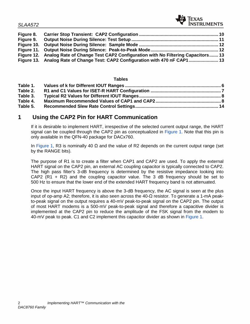
1 Using the CAP2 Pin for HART Communication If it is desirable to implement HART, irrespective of the selected current output range, the HART signal can be coupled through the CAP2 pin as conceptualized in Figure 1. Note that this pin is only available in the QFN-40 package for DACx760.
In Figure 1, R3 is nominally 40 Ω and the value of R2 depends on the current output range (set by the RANGE bits). The purpose of R1 is to create a filter when CAP1 and CAP2 are used. To apply the external HART signal on the CAP2 pin, an external AC coupling capacitor is typically connected to CAP2. The high pass filter's 3-dB frequency is determined by the resistive impedance looking into CAP2 (R1 + R2) and the coupling capacitor value. The 3 dB frequency should be set to 500 Hz to ensure that the lower end of the extended HART frequency band is not attenuated.
Once the input HART frequency is above the 3-dB frequency, the AC signal is seen at the plus input of op-amp A2; therefore, it is also seen across the 40-Ω resistor. To generate a 1-mA peak-to-peak signal on the output requires a 40-mV peak-to-peak signal on the CAP2 pin. The output of most HART modems is a 500-mV peak-to-peak signal and therefore a capacitive divider is implemented at the CAP2 pin to reduce the amplitude of the FSK signal from the modem to 40-mV peak to peak. C1 and C2 implement this capacitor divider as shown in Figure 1.
SLAA572
Implementing HART™ Communication with the DAC8760 Family 3
Figure 1. Implementing HART with a CAP2 Pin
1.1 Determining the Values of C1 and C2
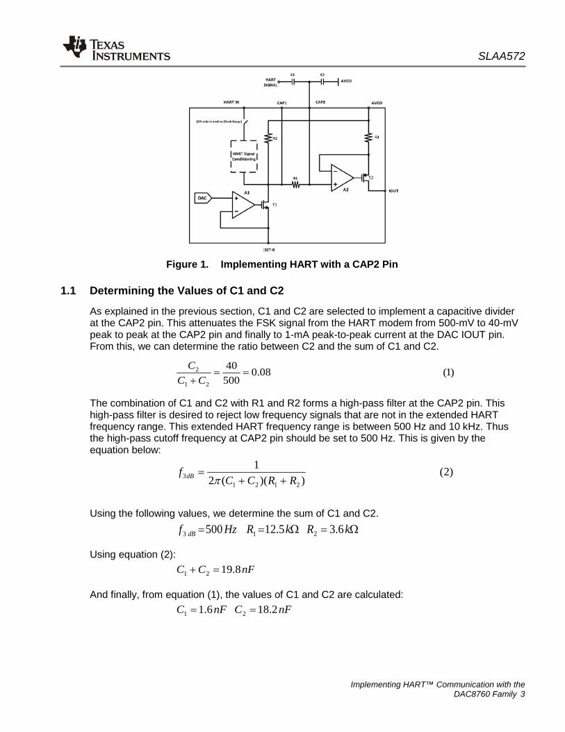
As explained in the previous section, C1 and C2 are selected to implement a capacitive divider at the CAP2 pin. This attenuates the FSK signal from the HART modem from 500-mV to 40-mV peak to peak at the CAP2 pin and finally to 1-mA peak-to-peak current at the DAC IOUT pin. From this, we can determine the ratio between C2 and the sum of C1 and C2.
The combination of C1 and C2 with R1 and R2 forms a high-pass filter at the CAP2 pin. This high-pass filter is desired to reject low frequency signals that are not in the extended HART frequency range. This extended HART frequency range is between 500 Hz and 10 kHz. Thus the high-pass cutoff frequency at CAP2 pin should be set to 500 Hz. This is given by the equation below:
Using the following values, we determine the sum of C1 and C2.
Using equation (2):
And finally, from equation (1), the values of C1 and C2 are calculated:
)1(08.050040
21
2 ==+CCC
)2())((2
1
21213 RRCC
f dB ++=
π
Ω=Ω== kRkRHzf dB 6.35.12500 213
nFCC 8.1921 =+
nFCnFC 2.186.1 21 ==

SLAA572
4 Implementing HART™ Communication with the DAC8760 Family
These capacitor values were calculated using the 0-mA to 24-mA current range. The other two ranges will result in similar values. Using 2 nF and 22 nF capacitors for C1 and C2, respectively, will work adequately for all the current ranges.
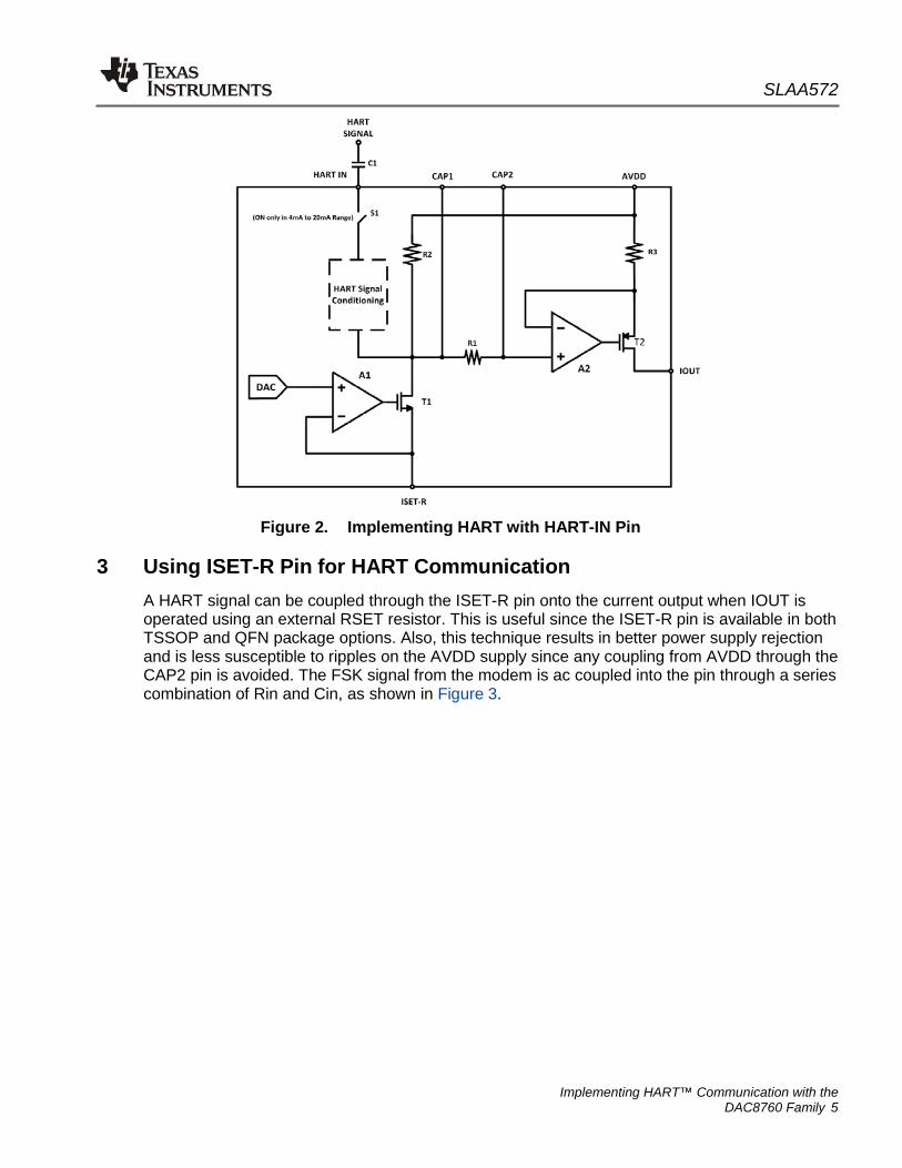
2 Using HART-IN Pin for HART Communication This method only works when the 4-mA to 20-mA output current range is selected by writing b’101 to bits [2:0] of the DAC8760 control register (address 0x55, also known as range bits). To use the HART-IN pin, HART has to first be enabled by writing b’1 to bit [4] of the configuration register (address 0x57, also known as HART_EN). This bit enables the HART interface and allows the HART signal to be coupled into the current output through the HART-IN pin. This is conceptualized in Figure 2 with switch S1 and the HART signal conditioning block.
The HART signal is ac coupled into the HART-IN pin though capacitor C1. The HART-IN pin has an equivalent series input resistance of 35 kΩ that is achieved after trimming at the factory. Similar to the case with the CAP2 pin, the ac coupling capacitor, C1, forms a high-pass filter with the input resistance of the HART-IN pin with the cutoff frequency shown in equation 3.
C1 is chosen so that the cutoff frequency of this filter is at 500Hz. This is to ensure that the lower end of the extended HART frequency band is covered and signals below 500 Hz are rejected. From the equation,
Any values of C1 close to 9 nF can be used. A 10 nF capacitor is suggested in most cases.
)3(2
1
13 CRin
f dB π=
nFC 1.91 =
SLAA572
Implementing HART™ Communication with the DAC8760 Family 5
Figure 2. Implementing HART with HART-IN Pin
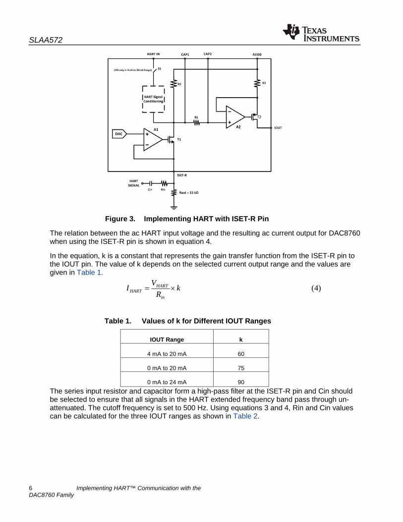
3 Using ISET-R Pin for HART Communication A HART signal can be coupled through the ISET-R pin onto the current output when IOUT is operated using an external RSET resistor. This is useful since the ISET-R pin is available in both TSSOP and QFN package options. Also, this technique results in better power supply rejection and is less susceptible to ripples on the AVDD supply since any coupling from AVDD through the CAP2 pin is avoided. The FSK signal from the modem is ac coupled into the pin through a series combination of Rin and Cin, as shown in Figure 3.
SLAA572
6 Implementing HART™ Communication with the DAC8760 Family
Figure 3. Implementing HART with ISET-R Pin
The relation between the ac HART input voltage and the resulting ac current output for DAC8760 when using the ISET-R pin is shown in equation 4.
In the equation, k is a constant that represents the gain transfer function from the ISET-R pin to the IOUT pin. The value of k depends on the selected current output range and the values are given in Table 1.
Table 1. Values of k for Different IOUT Ranges
IOUT Range
k
4 mA to 20 mA
60
0 mA to 20 mA
75
0 mA to 24 mA
90 The series input resistor and capacitor form a high-pass filter at the ISET-R pin and Cin should be selected to ensure that all signals in the HART extended frequency band pass through un-attenuated. The cutoff frequency is set to 500 Hz. Using equations 3 and 4, Rin and Cin values can be calculated for the three IOUT ranges as shown in Table 2.
)4(kR
VIin
HARTHART ×=
SLAA572
Implementing HART™ Communication with the DAC8760 Family 7
Table 2. R1 and C1 Values for ISET-R HART Configuration
IOUT Range Rin Cin 4 mA to 20 mA 30 kΩ 10.6 nF 0 mA to 20 mA 37.5 kΩ 8.5 nF 0 mA to 24 mA 45 kΩ 7 nF
Increasing the value of Rin will decrease the trans-conductance gain and vice versa. Increasing Cin will decrease the high pass cutoff frequency. Rin can be used as 37.5 kΩ and Cin as 8.5 nF for all the current ranges (values for the 0-mA to 20-mA range). In this case, a 500-mV peak-to-peak HART signal will result in a 0.8-mA peak-to-peak signal for the 4-mA to 20-mA range, 1-mA peak to peak for the 0-mA to 20-mA range and 1.2-mA peak to peak for the 0-mA to 24-mA range.
4 Digital Slew Rate Control and IOUT Filtering Capacitors The previous sections talk about how a signal from a HART modem can be coupled onto the current output of the DAC8760 using three different methods. However, this is not sufficient to complete the HART setup. It is necessary to reduce the IOUT slew rate to meet some of the HART compliance requirements as is discussed under the HART Compliance Tests section. This is done by using DAC8760’s digital slew rate control feature in combination with IOUT filtering capacitors. Details on the digital slew rate control feature can be found in the datasheet. The remaining sections take you through some calculations and finally some recommended settings are presented to achieve a HART-compliant system.
5 Using HART in Combination with IOUT Filtering Capacitors When using the DAC8760 QFN-40 package, a user can choose to connect capacitors to CAP1, CAP2, or both pins to limit the bandwidth, therefore, limiting the slew rate of the DAC current output. Using HART together with these IOUT filtering capacitors puts limitations on the values of CAP1 and CAP2 that can be used. This is mainly because CAP1 and CAP2 form a low-pass filter together with the DAC internal resistors when the HART signal is coupled either through the HART-IN pin or the ISET-R pin. The maximum capacitors used should allow HART signals in the HART extended frequency band to pass unattenuated, that is, (500 kHz–10 kHz). The low-pass cutoff frequencies are defined as in equation 5 for CAP1 and CAP2.
When CAP1 is connected:
When CAP2 is connected:
R1 is a 12.5-kΩ resistor and the value of R2 depends on the selected IOUT range. The typical R2 values are defined in Table 3.
𝑓3 𝑑𝐵 ≅1
2𝜋𝑅2𝐶𝐴𝑃1 (5𝑎)
𝑓3𝑑𝐵 ≅1
2𝜋(𝑅1 + 𝑅2)𝐶𝐴𝑃2 (5𝑏)
SLAA572
8 Implementing HART™ Communication with the DAC8760 Family
Table 3. Typical R2 Values for Different IOUT Ranges
IOUT Range
R2
4 mA to 20 mA
2.4 kΩ
0 mA to 20 mA
3.0 kΩ
0 mA to 24 mA
3.6 kΩ
For the 0-mA to 24-mA range:
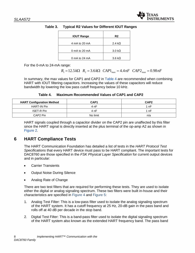
In summary, the max values for CAP1 and CAP2 in Table 4 are recommended when combining HART with IOUT filtering capacitors. Increasing the values of these capacitors will reduce bandwidth by lowering the low pass cutoff frequency below 10 kHz.
Table 4. Maximum Recommended Values of CAP1 and CAP2
HART Configuration Method CAP1 CAP2 HART-IN Pin 4 nF 1 nF ISET-R Pin 4 nF 1 nF CAP2 Pin No limit n/a
HART signals coupled through a capacitor divider on the CAP2 pin are unaffected by this filter since the HART signal is directly inserted at the plus terminal of the op-amp A2 as shown in Figure 2.
6 HART Compliance Tests The HART Communication Foundation has detailed a list of tests in the HART Protocol Test Specifications that every HART device must pass to be HART compliant. The important tests for DAC8760 are those specified in the FSK Physical Layer Specification for current output devices and in particular:
• Carrier Transients
• Output Noise During Silence
• Analog Rate of Change
There are two test filters that are required for performing these tests. They are used to isolate either the digital or analog signaling spectrum. These two filters were built in-house and their characteristics are specified in Figure 4 and Figure 5:
1. Analog Test Filter: This is a low-pass filter used to isolate the analog signaling spectrum of the HART system. It has a cutoff frequency at 25 Hz, 20-dB gain in the pass band and rolls off at 40 dB per decade in the stop band.
2. Digital Test Filter: This is a band-pass filter used to isolate the digital signaling spectrum of the HART system also known as the extended HART frequency band. The pass band
nFCAPnFCAPkRkR 98.024.416.35.12 maxmax21 ==Ω=Ω=

SLAA572
Implementing HART™ Communication with the DAC8760 Family 9
is between 500 Hz and 10 kHz and it has 20-dB gain in this region. The gain increases at 40 dB per decade before 500 Hz and rolls off at 20 dB per decade after 10 kHz.
Figure 4. Analog Test Filter Transfer Function
Figure 5. Digital Test Filter Transfer Function
6.1 Carrier Transients
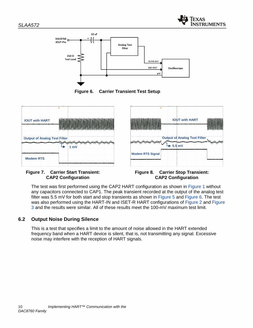
This test ensures that analog signaling is not affected by large transient spikes that are introduced at the start or the end of HART transmission. This test was carried out using a HART modem in combination with DAC8760. IOUT is loaded with a 250-Ω test resistor that is ac coupled to the input of the analog test filter, as shown in Figure 4. An oscilloscope is connected to monitor the input and output of the analog test filter. For the test, the DAC was first configured to output a fixed current. A HART ‘START’ or ‘STOP’ request is asserted using the HART modem and the oscilloscope signals are monitored from the start of HART transmission through the end, and 50 ms beyond the last HART signal transmitted. To pass the test, transient spikes measured at the start and the end of HART transmission must be limited to 10 mV (100 mV at the output of the analog test filter due to the gain of 10).
SLAA572
10 Implementing HART™ Communication with the DAC8760 Family
Figure 6. Carrier Transient Test Setup
Figure 7. Carrier Start Transient: CAP2 Configuration
Figure 8. Carrier Stop Transient: CAP2 Configuration
The test was first performed using the CAP2 HART configuration as shown in Figure 1 without any capacitors connected to CAP1. The peak transient recorded at the output of the analog test filter was 5.5 mV for both start and stop transients as shown in Figure 5 and Figure 6. The test was also performed using the HART-IN and ISET-R HART configurations of Figure 2 and Figure 3 and the results were similar. All of these results meet the 100-mV maximum test limit.
6.2 Output Noise During Silence
This is a test that specifies a limit to the amount of noise allowed in the HART extended frequency band when a HART device is silent, that is, not transmitting any signal. Excessive noise may interfere with the reception of HART signals.
IOUT with HART
Output of Analog Test Filter
Modem RTS
Modem RTS Signal
Output of Analog Test Filter
IOUT with HART
5.5 mV 1 mV
SLAA572
Implementing HART™ Communication with the DAC8760 Family 11
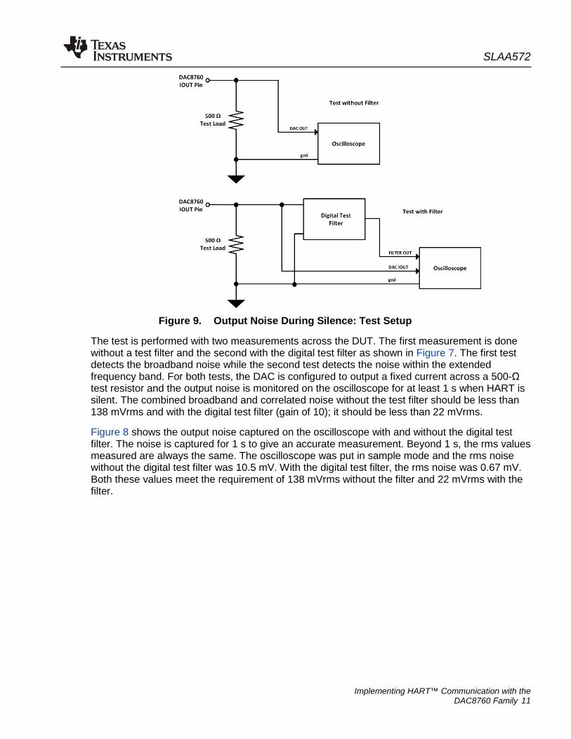
Figure 9. Output Noise During Silence: Test Setup
The test is performed with two measurements across the DUT. The first measurement is done without a test filter and the second with the digital test filter as shown in Figure 7. The first test detects the broadband noise while the second test detects the noise within the extended frequency band. For both tests, the DAC is configured to output a fixed current across a 500-Ω test resistor and the output noise is monitored on the oscilloscope for at least 1 s when HART is silent. The combined broadband and correlated noise without the test filter should be less than 138 mVrms and with the digital test filter (gain of 10); it should be less than 22 mVrms.
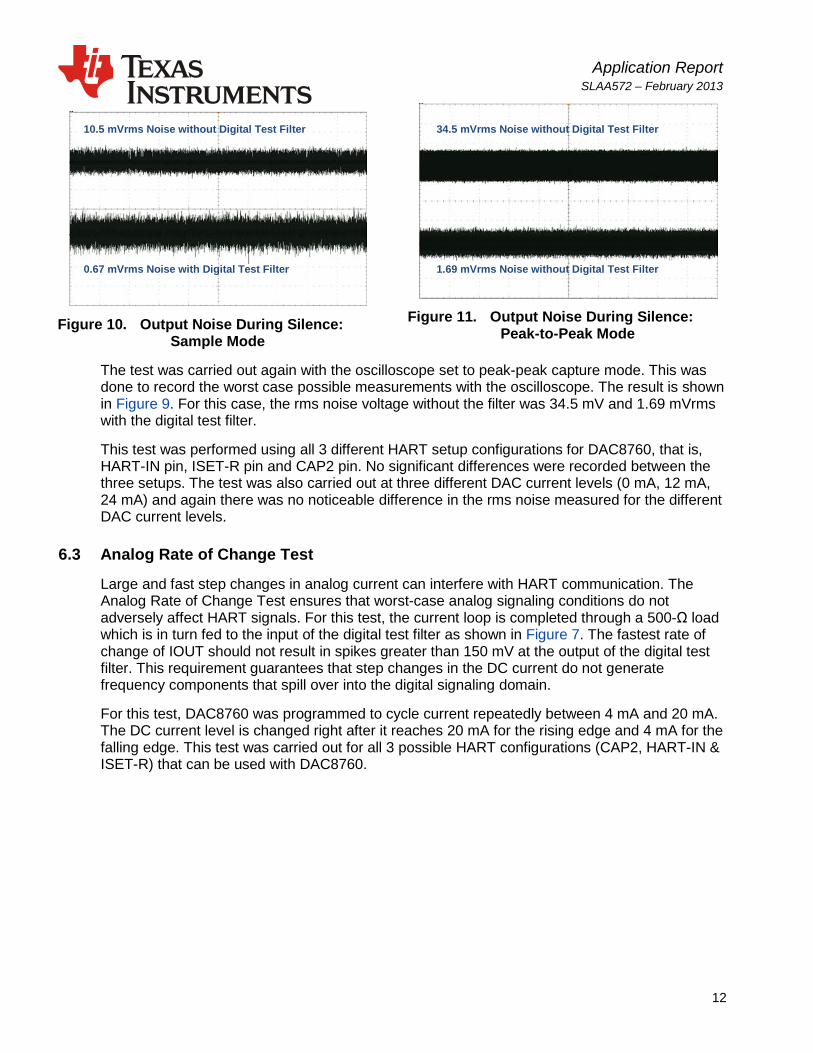
Figure 8 shows the output noise captured on the oscilloscope with and without the digital test filter. The noise is captured for 1 s to give an accurate measurement. Beyond 1 s, the rms values measured are always the same. The oscilloscope was put in sample mode and the rms noise without the digital test filter was 10.5 mV. With the digital test filter, the rms noise was 0.67 mV. Both these values meet the requirement of 138 mVrms without the filter and 22 mVrms with the filter.
Application Report SLAA572 – February 2013
12
Figure 10. Output Noise During Silence: Sample Mode
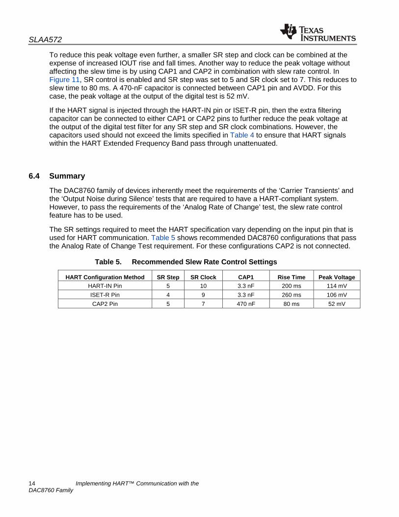
Figure 11. Output Noise During Silence: Peak-to-Peak Mode
The test was carried out again with the oscilloscope set to peak-peak capture mode. This was done to record the worst case possible measurements with the oscilloscope. The result is shown in Figure 9. For this case, the rms noise voltage without the filter was 34.5 mV and 1.69 mVrms with the digital test filter.
This test was performed using all 3 different HART setup configurations for DAC8760, that is, HART-IN pin, ISET-R pin and CAP2 pin. No significant differences were recorded between the three setups. The test was also carried out at three different DAC current levels (0 mA, 12 mA, 24 mA) and again there was no noticeable difference in the rms noise measured for the different DAC current levels.
6.3 Analog Rate of Change Test
Large and fast step changes in analog current can interfere with HART communication. The Analog Rate of Change Test ensures that worst-case analog signaling conditions do not adversely affect HART signals. For this test, the current loop is completed through a 500-Ω load which is in turn fed to the input of the digital test filter as shown in Figure 7. The fastest rate of change of IOUT should not result in spikes greater than 150 mV at the output of the digital test filter. This requirement guarantees that step changes in the DC current do not generate frequency components that spill over into the digital signaling domain.
For this test, DAC8760 was programmed to cycle current repeatedly between 4 mA and 20 mA. The DC current level is changed right after it reaches 20 mA for the rising edge and 4 mA for the falling edge. This test was carried out for all 3 possible HART configurations (CAP2, HART-IN & ISET-R) that can be used with DAC8760.
10.5 mVrms Noise without Digital Test Filter
0.67 mVrms Noise with Digital Test Filter 1.69 mVrms Noise without Digital Test Filter
34.5 mVrms Noise without Digital Test Filter

SLAA572
Implementing HART™ Communication with the DAC8760 Family 13
Figure 12. Analog Rate of Change Test CAP2 Configuration with No Filtering Capacitors
In order to meet the analog rate of change specification, IOUT slew rate has to be reduced to ensure its bandwidth is limited to about 25 Hz. This can be done by combining DAC8760’s digital slew rate feature, together with the use of the CAP1 and CAP2 filtering capacitors. Using only CAP1 and CAP2 would require very large capacitors (> 100 µF) to limit the IOUT bandwidth to 25 Hz, and is not practical. It is possible to meet this requirement by only using the digital slew rate feature but only at extremely slow digital slew rate settings.
Figure 10 shows IOUT cycling between 4 mA and 20 mA and shows the response at the output of the digital test filter. Slew rate was enabled in the control register. SR step was set to 4 and SR clock set to 7. This translates to a rise or fall time of 160 ms when slew rate control is enabled up from 8 µs when slew rate control is disabled. The peak voltage measured at the output of the digital test filter is 96 mV using these settings and this satisfies the HART requirement.
Figure 13. Analog Rate of Change Test: CAP2 Configuration with 470 nF CAP1
4 mA to 20 mA, 500-Ω load SR STEP: 4 SR CLK: 7 CAP2 HART Configuration
96 mV
96 mV
4 mA
20 mA
Horizontal Scale: 40 ms/div
Slew time: 160 ms
Filter Output
IOUT
Horizontal Scale: 20 ms/div
52 mV
Slew time: 80 ms 20 mA
4 mA to 20 mA, 500-Ω load SR STEP: 5 SR CLK: 7 CAP1: 470 nF CAP2 HART Configuration
Filter Output
IOUT
48 mV
4 mA
SLAA572
14 Implementing HART™ Communication with the DAC8760 Family
To reduce this peak voltage even further, a smaller SR step and clock can be combined at the expense of increased IOUT rise and fall times. Another way to reduce the peak voltage without affecting the slew time is by using CAP1 and CAP2 in combination with slew rate control. In Figure 11, SR control is enabled and SR step was set to 5 and SR clock set to 7. This reduces to slew time to 80 ms. A 470-nF capacitor is connected between CAP1 pin and AVDD. For this case, the peak voltage at the output of the digital test is 52 mV.
If the HART signal is injected through the HART-IN pin or ISET-R pin, then the extra filtering capacitor can be connected to either CAP1 or CAP2 pins to further reduce the peak voltage at the output of the digital test filter for any SR step and SR clock combinations. However, the capacitors used should not exceed the limits specified in Table 4 to ensure that HART signals within the HART Extended Frequency Band pass through unattenuated.
6.4 Summary
The DAC8760 family of devices inherently meet the requirements of the ‘Carrier Transients’ and the ‘Output Noise during Silence’ tests that are required to have a HART-compliant system. However, to pass the requirements of the ‘Analog Rate of Change’ test, the slew rate control feature has to be used.
The SR settings required to meet the HART specification vary depending on the input pin that is used for HART communication. Table 5 shows recommended DAC8760 configurations that pass the Analog Rate of Change Test requirement. For these configurations CAP2 is not connected.
Table 5. Recommended Slew Rate Control Settings
HART Configuration Method SR Step SR Clock CAP1 Rise Time Peak Voltage HART-IN Pin 5 10 3.3 nF 200 ms 114 mV ISET-R Pin 4 9 3.3 nF 260 ms 106 mV CAP2 Pin 5 7 470 nF 80 ms 52 mV
IMPORTANT NOTICETexas Instruments Incorporated and its subsidiaries (TI) reserve the right to make corrections, enhancements, improvements and otherchanges to its semiconductor products and services per JESD46, latest issue, and to discontinue any product or service per JESD48, latestissue. Buyers should obtain the latest relevant information before placing orders and should verify that such information is current andcomplete. All semiconductor products (also referred to herein as “components”) are sold subject to TI’s terms and conditions of salesupplied at the time of order acknowledgment.TI warrants performance of its components to the specifications applicable at the time of sale, in accordance with the warranty in TI’s termsand conditions of sale of semiconductor products. Testing and other quality control techniques are used to the extent TI deems necessaryto support this warranty. Except where mandated by applicable law, testing of all parameters of each component is not necessarilyperformed.TI assumes no liability for applications assistance or the design of Buyers’ products. Buyers are responsible for their products andapplications using TI components. To minimize the risks associated with Buyers’ products and applications, Buyers should provideadequate design and operating safeguards.TI does not warrant or represent that any license, either express or implied, is granted under any patent right, copyright, mask work right, orother intellectual property right relating to any combination, machine, or process in which TI components or services are used. Informationpublished by TI regarding third-party products or services does not constitute a license to use such products or services or a warranty orendorsement thereof. Use of such information may require a license from a third party under the patents or other intellectual property of thethird party, or a license from TI under the patents or other intellectual property of TI.Reproduction of significant portions of TI information in TI data books or data sheets is permissible only if reproduction is without alterationand is accompanied by all associated warranties, conditions, limitations, and notices. TI is not responsible or liable for such altereddocumentation. Information of third parties may be subject to additional restrictions.Resale of TI components or services with statements different from or beyond the parameters stated by TI for that component or servicevoids all express and any implied warranties for the associated TI component or service and is an unfair and deceptive business practice.TI is not responsible or liable for any such statements.Buyer acknowledges and agrees that it is solely responsible for compliance with all legal, regulatory and safety-related requirementsconcerning its products, and any use of TI components in its applications, notwithstanding any applications-related information or supportthat may be provided by TI. Buyer represents and agrees that it has all the necessary expertise to create and implement safeguards whichanticipate dangerous consequences of failures, monitor failures and their consequences, lessen the likelihood of failures that might causeharm and take appropriate remedial actions. Buyer will fully indemnify TI and its representatives against any damages arising out of the useof any TI components in safety-critical applications.In some cases, TI components may be promoted specifically to facilitate safety-related applications. With such components, TI’s goal is tohelp enable customers to design and create their own end-product solutions that meet applicable functional safety standards andrequirements. Nonetheless, such components are subject to these terms.No TI components are authorized for use in FDA Class III (or similar life-critical medical equipment) unless authorized officers of the partieshave executed a special agreement specifically governing such use.Only those TI components which TI has specifically designated as military grade or “enhanced plastic” are designed and intended for use inmilitary/aerospace applications or environments. Buyer acknowledges and agrees that any military or aerospace use of TI componentswhich have not been so designated is solely at the Buyer's risk, and that Buyer is solely responsible for compliance with all legal andregulatory requirements in connection with such use.TI has specifically designated certain components as meeting ISO/TS16949 requirements, mainly for automotive use. In any case of use ofnon-designated products, TI will not be responsible for any failure to meet ISO/TS16949.Products ApplicationsAudio www.ti.com/audio Automotive and Transportation www.ti.com/automotiveAmplifiers amplifier.ti.com Communications and Telecom www.ti.com/communicationsData Converters dataconverter.ti.com Computers and Peripherals www.ti.com/computersDLP® Products www.dlp.com Consumer Electronics www.ti.com/consumer-appsDSP dsp.ti.com Energy and Lighting www.ti.com/energyClocks and Timers www.ti.com/clocks Industrial www.ti.com/industrialInterface interface.ti.com Medical www.ti.com/medicalLogic logic.ti.com Security www.ti.com/securityPower Mgmt power.ti.com Space, Avionics and Defense www.ti.com/space-avionics-defenseMicrocontrollers microcontroller.ti.com Video and Imaging www.ti.com/videoRFID www.ti-rfid.comOMAP Applications Processors www.ti.com/omap TI E2E Community e2e.ti.comWireless Connectivity www.ti.com/wirelessconnectivity
Mailing Address: Texas Instruments, Post Office Box 655303, Dallas, Texas 75265Copyright © 2014, Texas Instruments Incorporated