implementing an lcd using the pic16f1947 …ww1.microchip.com/downloads/en/appnotes/01354a.pdf ·...
TRANSCRIPT
AN1354Implementing an LCD Using the PIC16F1947 Microcontroller
INTRODUCTION
This application note reviews the process andprocedure of implementing a segmented LCD using thePIC16F1947 microcontroller (MCU) in an exampleapplication. The example application will be anelectronic combination lock. As this application isimplemented, the configuration and low-power optionsassociated with the PIC16F1947 LCD module will bediscussed.
GETTING STARTED
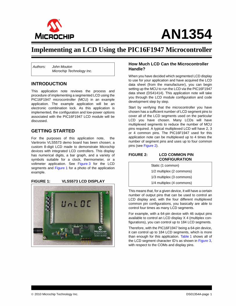
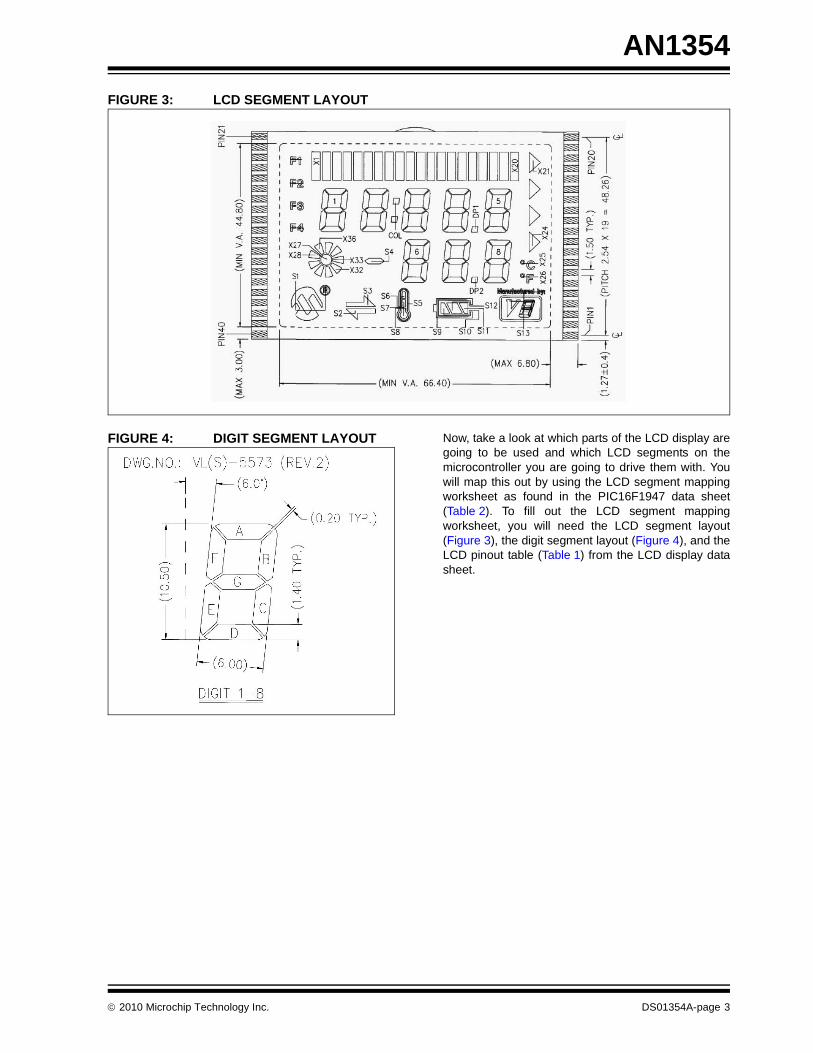
For the purposes of this application note, theVaritronix VLS5573 demo board has been chosen; acustom 8-digit LCD made to demonstrate Microchipdevices with integrated LCD controllers. This displayhas numerical digits, a bar graph, and a variety ofsymbols suitable for a clock, thermometer, or avoltmeter application. See Figure 3 for the LCDsegments and Figure 1 for a photo of the applicationexample.
FIGURE 1: VLS5573 LCD DISPLAY
How Much LCD Can the Microcontroller Handle?
When you have decided which segmented LCD displayto use for your application and have acquired the LCDdata sheet (from the manufacturer), you can beginsetting up the MCU to run the LCD via the PIC16F1947data sheet (DS41414). This application note will takeyou through the LCD module configuration and codedevelopment step by step.
Start by verifying that the microcontroller you havechosen has a sufficient number of LCD segment pins tocover all of the LCD segments used on the particularLCD you have chosen. Many LCDs will havemultiplexed segments to reduce the number of MCUpins required. A typical multiplexed LCD will have 2, 3or 4 common pins. The PIC16F1947 used for thisapplication note can be multiplexed up to 4 times thenumber of segment pins and uses up to four commonpins (see Figure 2).
FIGURE 2: LCD COMMON PIN CONFIGURATION
This means that, for a given device, it will have a certainnumber of output pins that can be used to control anLCD display and, with the four different multiplexedcommon pin configurations, you basically are able tocontrol four times as many LCD segments.
For example, with a 64-pin device with 46 output pinsavailable to control an LCD display X 4 (multiplex con-figurations), you can control up to 184 LCD segments.
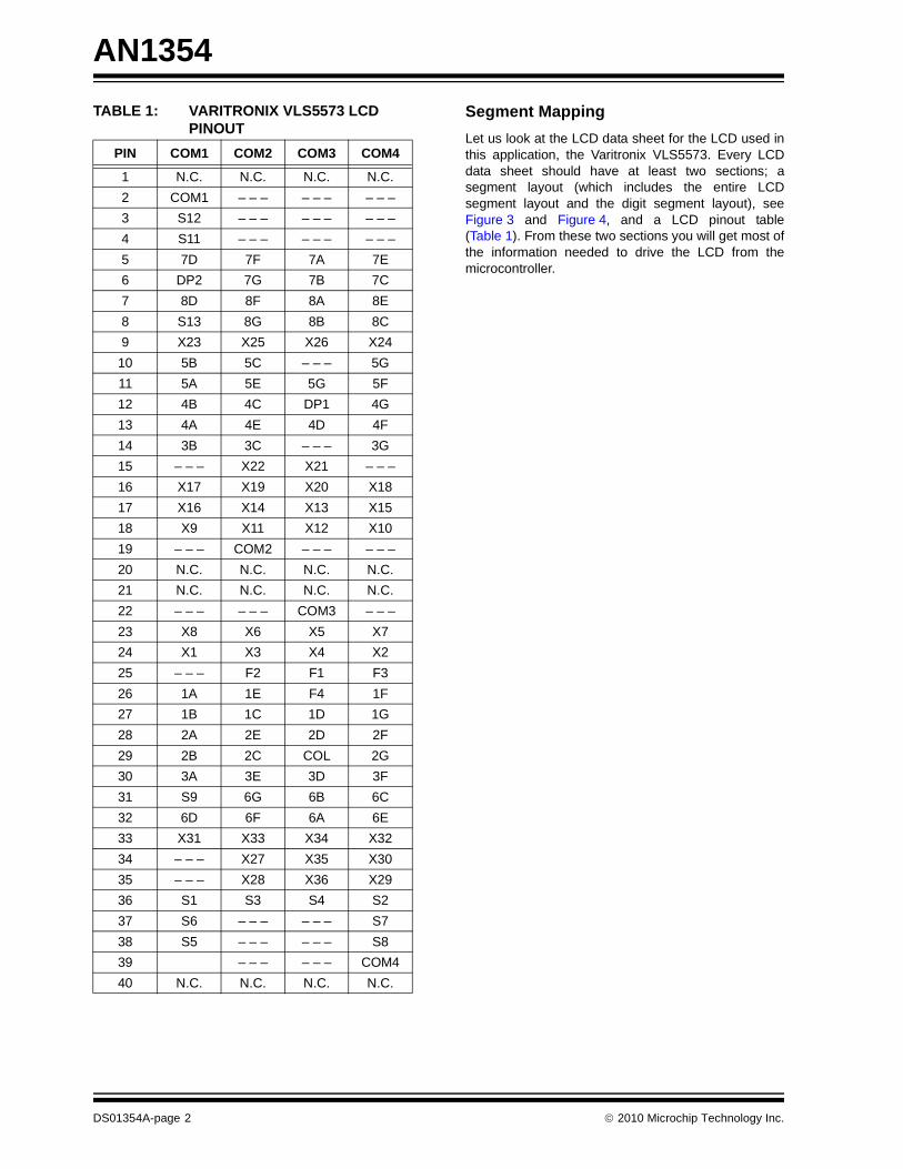
Therefore, with the PIC16F1947 being a 64-pin device,it can control up to 184 LCD segments, which is morethan enough for this application. Table 1 shows all ofthe LCD segment character ID’s as shown in Figure 3,with respect to the COMs and display pins.
Authors: John MoutonMicrochip Technology Inc.
Static (1 common)
1/2 multiplex (2 commons)
1/3 multiplex (3 commons)
1/4 multiplex (4 commons)
2010 Microchip Technology Inc. DS01354A-page 1
AN1354
TABLE 1: VARITRONIX VLS5573 LCD PINOUT
Segment Mapping
Let us look at the LCD data sheet for the LCD used inthis application, the Varitronix VLS5573. Every LCDdata sheet should have at least two sections; asegment layout (which includes the entire LCDsegment layout and the digit segment layout), seeFigure 3 and Figure 4, and a LCD pinout table(Table 1). From these two sections you will get most ofthe information needed to drive the LCD from themicrocontroller.
PIN COM1 COM2 COM3 COM4
1 N.C. N.C. N.C. N.C.
2 COM1 – – – – – – – – –
3 S12 – – – – – – – – –
4 S11 – – – – – – – – –
5 7D 7F 7A 7E
6 DP2 7G 7B 7C
7 8D 8F 8A 8E
8 S13 8G 8B 8C
9 X23 X25 X26 X24
10 5B 5C – – – 5G
11 5A 5E 5G 5F
12 4B 4C DP1 4G
13 4A 4E 4D 4F
14 3B 3C – – – 3G
15 – – – X22 X21 – – –
16 X17 X19 X20 X18
17 X16 X14 X13 X15
18 X9 X11 X12 X10
19 – – – COM2 – – – – – –
20 N.C. N.C. N.C. N.C.
21 N.C. N.C. N.C. N.C.
22 – – – – – – COM3 – – –
23 X8 X6 X5 X7
24 X1 X3 X4 X2
25 – – – F2 F1 F3
26 1A 1E F4 1F
27 1B 1C 1D 1G
28 2A 2E 2D 2F
29 2B 2C COL 2G
30 3A 3E 3D 3F
31 S9 6G 6B 6C
32 6D 6F 6A 6E
33 X31 X33 X34 X32
34 – – – X27 X35 X30
35 – – – X28 X36 X29
36 S1 S3 S4 S2
37 S6 – – – – – – S7
38 S5 – – – – – – S8
39 – – – – – – COM4
40 N.C. N.C. N.C. N.C.
DS01354A-page 2 2010 Microchip Technology Inc.
AN1354
FIGURE 3: LCD SEGMENT LAYOUT
FIGURE 4: DIGIT SEGMENT LAYOUT Now, take a look at which parts of the LCD display aregoing to be used and which LCD segments on themicrocontroller you are going to drive them with. Youwill map this out by using the LCD segment mappingworksheet as found in the PIC16F1947 data sheet(Table 2). To fill out the LCD segment mappingworksheet, you will need the LCD segment layout(Figure 3), the digit segment layout (Figure 4), and theLCD pinout table (Table 1) from the LCD display datasheet.
2010 Microchip Technology Inc. DS01354A-page 3

AN1354
TABLE 2: LCD SEGMENT MAPPING WORKSHEET
LCD Function
COM0 COM1 COM2 COM3
LCDDATAxAddress
LCD Segment
LCDDATAxAddress
LCD Segment
LCDDATAxAddress
LCD Segment
LCDDATAxAddress
LCD Segment
SEG0 LCDDATA0, 0 LCDDATA3, 0 LCDDATA6, 0 LCDDATA9, 0
SEG1 LCDDATA0, 1 LCDDATA3, 1 LCDDATA6, 1 LCDDATAA9, 1
SEG2 LCDDATA0, 2 LCDDATA3, 2 LCDDATA6, 2 LCDDATAA9, 2
SEG3 LCDDATA0, 3 LCDDATA3, 3 LCDDATA6, 3 LCDDATAA9, 3
SEG4 LCDDATA0, 4 LCDDATA3, 4 LCDDATA6, 4 LCDDATAA9, 4
SEG5 LCDDATA0, 5 LCDDATA3, 5 LCDDATA6, 5 LCDDATAA9, 5
SEG6 LCDDATA0, 6 LCDDATA3, 6 LCDDATA6, 6 LCDDATAA9, 6
SEG7 LCDDATA0, 7 LCDDATA3, 7 LCDDATA6, 7 LCDDATAA9, 7
SEG8 LCDDATA1, 0 LCDDATA4, 0 LCDDATA7, 0 LCDDATA10, 0
SEG9 LCDDATA1, 1 LCDDATA4, 1 LCDDATA7, 1 LCDDATA10, 1
SEG10 LCDDATA1, 2 LCDDATA4, 2 LCDDATA7, 2 LCDDATA10, 2
SEG11 LCDDATA1, 3 LCDDATA4, 3 LCDDATA7, 3 LCDDATA10, 3
SEG12 LCDDATA1, 4 LCDDATA4, 4 LCDDATA7, 4 LCDDATA10, 4
SEG13 LCDDATA1, 5 LCDDATA4, 5 LCDDATA7, 5 LCDDATA10, 5
SEG14 LCDDATA1, 6 LCDDATA4, 6 LCDDATA7, 6 LCDDATA10, 6
SEG15 LCDDATA1, 7 LCDDATA4, 7 LCDDATA7, 7 LCDDATA10, 7
SEG16 LCDDATA2, 0 LCDDATA5, 0 LCDDATA8, 0 LCDDATA11, 0
SEG17 LCDDATA2, 1 LCDDATA5, 1 LCDDATA8, 1 LCDDATA11, 1
SEG18 LCDDATA2, 2 LCDDATA5, 2 LCDDATA8, 2 LCDDATA11, 2
SEG19 LCDDATA2, 3 LCDDATA5, 3 LCDDATA8, 3 LCDDATA11, 3
SEG20 LCDDATA2, 4 LCDDATA5, 4 LCDDATA8, 4 LCDDATA11, 4
SEG21 LCDDATA2, 5 LCDDATA5, 5 LCDDATA8, 5 LCDDATA11, 5
SEG22 LCDDATA2, 6 LCDDATA5, 6 LCDDATA8, 6 LCDDATA11, 6
SEG23 LCDDATA2, 7 LCDDATA5, 7 LCDDATA8, 7 LCDDATA11, 7
SEG24 LCDDATA12, 0 LCDDATA15, 0 LCDDATA18, 0 LCDDATA21, 0
SEG25 LCDDATA12, 1 LCDDATA15, 1 LCDDATA18, 1 LCDDATA21, 1
SEG26 LCDDATA12, 2 LCDDATA15, 2 LCDDATA18, 2 LCDDATA21, 2
SEG27 LCDDATA12, 3 LCDDATA15, 3 LCDDATA18, 3 LCDDATA21, 3
SEG28 LCDDATA12, 4 LCDDATA15, 4 LCDDATA18, 4 LCDDATA21, 4
SEG29 LCDDATA12, 5 LCDDATA15, 5 LCDDATA18, 5 LCDDATA21, 5
SEG30 LCDDATA12, 6 LCDDATA15, 6 LCDDATA18, 6 LCDDATA21, 6
SEG31 LCDDATA12, 7 LCDDATA15, 7 LCDDATA18, 7 LCDDATA21, 7
SEG32 LCDDATA13, 0 LCDDATA16, 0 LCDDATA19, 0 LCDDATA22, 0
SEG33 LCDDATA13, 1 LCDDATA16, 1 LCDDATA19, 1 LCDDATA22, 1
SEG34 LCDDATA13, 2 LCDDATA16, 2 LCDDATA19, 2 LCDDATA22, 2
SEG35 LCDDATA13, 3 LCDDATA16, 3 LCDDATA19, 3 LCDDATA22, 3
SEG36 LCDDATA13, 4 LCDDATA16, 4 LCDDATA19, 4 LCDDATA22, 4
SEG37 LCDDATA13, 5 LCDDATA16, 5 LCDDATA19, 5 LCDDATA22, 5
SEG38 LCDDATA13, 6 LCDDATA16, 6 LCDDATA19, 6 LCDDATA22, 6
SEG39 LCDDATA13, 7 LCDDATA16, 7 LCDDATA19, 7 LCDDATA22, 7
SEG40 LCDDATA14, 0 LCDDATA17, 0 LCDDATA20, 0 LCDDATA23, 0
SEG41 LCDDATA14, 1 LCDDATA17, 1 LCDDATA20, 1 LCDDATA23, 1
SEG42 LCDDATA14, 2 LCDDATA17, 2 LCDDATA20, 2 LCDDATA23, 2
SEG43 LCDDATA14, 3 LCDDATA17, 3 LCDDATA20, 3 LCDDATA23, 3
SEG44 LCDDATA14, 4 LCDDATA17, 4 LCDDATA20, 4 LCDDATA23, 4
SEG45 LCDDATA14, 5 LCDDATA17, 5 LCDDATA20, 5 LCDDATA23, 5
DS01354A-page 4 2010 Microchip Technology Inc.

AN1354
The LCD segment layout shows all of the LCD’s displayfeatures, location on the display and their segment IDs,as shown in Figure 3. This layout also shows howmany digits can be displayed and each digit’s individualsegment layout, as shown in Figure 4. Table 1 showsall of the LCD display segment IDs, which commonsthey are on, and which LCD pins they are on. This willallow you to physically connect the specificmicrocontroller segment pins to the correct LCD
display segment pin. The LCD segment mappingworksheet, Table 2, will help you keep track of whichmicrocontroller LCD segment will drive a particularLCD display segment ID of your choosing and showsyou which LCDDATA register bit will control theparticular segment. See Table 3 for a completed LCDsegment map for the electronic combination lockapplication.
LCD Module Configuration
Now, take a look at the registers used to set up the LCDmodule in the PIC16F1947 device you are using. TheLCD module contains the following registers:
- LCD Control register (LCDCON)- LCD Phase register (LCDPS)- LCD Reference Ladder register (LCDRL)- LCD Contrast Control register (LCDCST)- LCD Reference Voltage Control register
(LCDREF)- LCD Segment Enable registers (LCDSEn)- LCD Data registers (LCDDATAn)
See Example 1 for the LCD module register settings asused in this application example.
TABLE 3: COMPLETED LCD SEGMENT MAPPING WORKSHEET
LCD Function
COM0 COM1 COM2 COM3
LCDDATAxAddress
LCD Segment
LCDDATAxAddress
LCD Segment
LCDDATAxAddress
LCD Segment
LCDDATAxAddress
LCD Segment
SEG0 LCDDATA0, 0 LCDDATA3, 0 LCDDATA6, 0 LCDDATA9, 0
SEG1 LCDDATA0, 1 1A LCDDATA3, 1 1E LCDDATA6, 1 F4 LCDDATAA9, 1 1F
SEG2 LCDDATA0, 2 – LCDDATA3, 2 F2 LCDDATA6, 2 F1 LCDDATAA9, 2 F3
SEG3 LCDDATA0, 3 1B LCDDATA3, 3 1C LCDDATA6, 3 1D LCDDATAA9, 3 1G
SEG4 LCDDATA0, 4 5B LCDDATA3, 4 5C LCDDATA6, 4 – LCDDATAA9, 4 5G
SEG5 LCDDATA0, 5 5A LCDDATA3, 5 5E LCDDATA6, 5 5D LCDDATAA9, 5 5F
SEG6 LCDDATA0, 6 2A LCDDATA3, 6 2E LCDDATA6, 6 2D LCDDATAA9, 6 2F
SEG7 LCDDATA0, 7 LCDDATA3, 7 LCDDATA6, 7 LCDDATAA9, 7
SEG8 LCDDATA1, 0 LCDDATA4, 0 LCDDATA7, 0 LCDDATA10, 0
SEG9 LCDDATA1, 1 LCDDATA4, 1 LCDDATA7, 1 LCDDATA10, 1
SEG10 LCDDATA1, 2 LCDDATA4, 2 LCDDATA7, 2 LCDDATA10, 2
SEG11 LCDDATA1, 3 3A LCDDATA4, 3 3E LCDDATA7, 3 3D LCDDATA10, 3 3F
SEG12 LCDDATA1, 4 LCDDATA4, 4 LCDDATA7, 4 LCDDATA10, 4
SEG13 LCDDATA1, 5 LCDDATA4, 5 LCDDATA7, 5 LCDDATA10, 5
SEG14 LCDDATA1, 6 LCDDATA4, 6 LCDDATA7, 6 LCDDATA10, 6
SEG15 LCDDATA1, 7 LCDDATA4, 7 LCDDATA7, 7 LCDDATA10, 7
SEG16 LCDDATA2, 0 2B LCDDATA5, 0 2C LCDDATA8, 0 – LCDDATA11, 0 2G
SEG17 LCDDATA2, 1 LCDDATA5, 1 LCDDATA8, 1 LCDDATA11, 1
SEG18 LCDDATA2, 2 S1 LCDDATA5, 2 LCDDATA8, 2 LCDDATA11, 2
SEG19 LCDDATA2, 3 LCDDATA5, 3 LCDDATA8, 3 LCDDATA11, 3
SEG20 LCDDATA2, 4 LCDDATA5, 4 LCDDATA8, 4 LCDDATA11, 4
SEG21 LCDDATA2, 5 4B LCDDATA5, 5 4C LCDDATA8, 5 – LCDDATA11, 5 4G
SEG22 LCDDATA2, 6 4A LCDDATA5, 6 4E LCDDATA8, 6 4D LCDDATA11, 6 4F
SEG23 LCDDATA2, 7 3B LCDDATA5, 7 3C LCDDATA8, 7 – LCDDATA11, 7 3G
Note: The LCD display segment IDs can bedriven by any microcontroller LCDsegment function of your choosing.
For example:
Microcontroller LCD function LCD Segments
SEG1 1A,1E,F4,1F
or SEG13 1A,1E,F4,1F
Note: However, the choice of LCD segment pinswill likely be determined by the PCB layoutof your application. Your source code willinclude functions that map to the appropri-ate bits in the LCDDATA registers.
2010 Microchip Technology Inc. DS01354A-page 5

AN1354
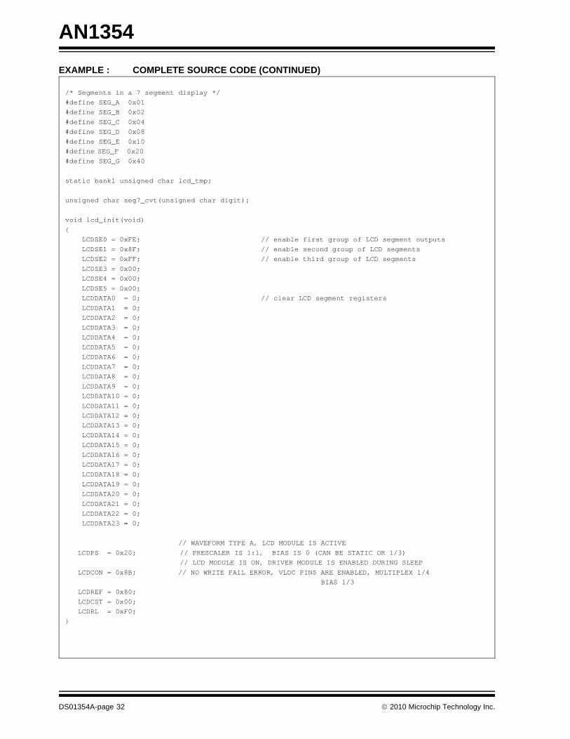
EXAMPLE 1: INITIALIZATION OF THE LCD MODULE
void lcd_init(void){ LCDSE0 = 0xFE; LCDSE1 = 0x8F; LCDSE2 = 0xFF; LCDSE3 = 0x00; LCDSE4 = 0x00; LCDSE5 = 0x00;
// enable first group of LCD segment outputs// enable second group of LCD segments// enable third group of LCD segments
LCDDATA0 = 0; LCDDATA1 = 0; LCDDATA2 = 0; LCDDATA3 = 0; LCDDATA4 = 0; LCDDATA5 = 0; LCDDATA6 = 0; LCDDATA7 = 0; LCDDATA8 = 0; LCDDATA9 = 0; LCDDATA10 = 0; LCDDATA11 = 0; LCDDATA12 = 0; LCDDATA13 = 0; LCDDATA14 = 0; LCDDATA15 = 0; LCDDATA16 = 0; LCDDATA17 = 0; LCDDATA18 = 0; LCDDATA19 = 0; LCDDATA20 = 0; LCDDATA21 = 0; LCDDATA22 = 0; LCDDATA23 = 0;
// clear LCD segment registers
// clear LCD segment registers
// WAVEFORM TYPE A, LCD MODULE IS ACTIVE LCDPS = 0x20; // PRESCALER IS 1:1, BIAS IS 0 (CAN BE STATIC OR 1/3)
// LCD MODULE IS ON, DRIVER MODULE IS ENABLED DURING SLEEP LCDCON = 0x8B; // NO WRITE FAIL ERROR, VLDC PINS ARE ENABLED, MULTIPLEX 1/4 BIAS 1/3
LCDREF = 0x80;
LCDCST = 0x00;
LCDRL = 0xF0;
}
DS01354A-page 6 2010 Microchip Technology Inc.

AN1354
LCD CONTROL REGISTER (LCDCON)
For this application, this register is used to:
- turn the LCD module on,
- have the LCD module off while the microcontroller is in Sleep mode,
- clock source the LCD using the Timer1 oscillator T1OSC and,
- have the LCD segments configured for 1/4 multiplex to give us the maximum number of LCD segments for this device (184 segments) at 1/3 bias.
Clock Sources
The LCD module has 3 possible clock sources: FOSC/256, T1OSC and LFINTOSC. The first clock source isthe system clock (FOSC) divided by 256. This dividerratio is chosen to provide about 1 kHz output when thesystem clock is 8 MHz. This source is commonly usedunless the LCD needs to run while the processor is inSleep mode, then the second or third clock sourcesshould be used. The second clock source is theT1OSC. This clock source will also give about 1 kHzwhen a 32 kHz crystal is used with the Timer1oscillator. The third clock source is the 31 kHz Low-Frequency Internal Oscillator (LFINTOSC), which alsoprovides approximately 1 kHz output.
Which clock source is better for low power? Thatdepends on the microcontroller and the LCD modulebeing used. For the purpose of this application, usingthe PIC16F1947 in Sleep mode, T1OSC or LFINTOSCcan be used. However, if you look in the electricalspecification section of the data sheet (DS41414) youwill see that using the T1OSC clock will consume theleast amount of current of the two. When themicrocontroller is not in Sleep mode and you are usingWatchdog Timer (WDT), the LFINTOSC has the lowercurrent consumption. But, if you are already using theT1OSC for Sleep mode, use it when you are not inSleep mode. The difference in current consumption isminimal and it does not make sense to change it.
Drive Modes
LCD panels come in many flavors depending on theapplication and the operating environment. LCDs canbe classified in two ways. LCDs come in static (ordirect) drive or multiplex drive variations. Static drivedisplays use only one common or backplane signal.Every pixel has its own segment and frontplane line.The common line acts as an “activation” signal,preparing all the pixels that it touches to be turned onby respective segment lines. The segment lines act asa “selector” signal, specifying whether a pixel is turnedON or OFF. When the common line is not activated, thesegment lines have no effect on the pixel state.
Frequencies for static drive displays are typicallybetween 30 Hz and 100 Hz, depending on display sizeand design. Displays can operate at higherfrequencies, but this increases power consumption.LCDs mimic a capacitive load, which reduces the loadimpedance as frequency increases. However,operation below 30 Hz usually results in visible flickerof the segments. LCDs can be overdriven by acombination of voltage, frequency and lower contrast athigher frequencies, which result in cross talk or“ghosting”. Ghosting is the appearance or partialactivation of an “off” segment. This condition occurswhen high drive voltage and frequency are applied.Because the current is directly proportional to thefrequency, the voltage-frequency product must not beexceeded. It is also important to connect all unusedsegments to the backplane, and not allow them to float.
The main advantage of static drive is that it is simple toimplement. You only have to worry about whichsegment line to turn on and off, while activating thecommon signal all the time.
Another advantage is that voltage levels can go fromrail to rail and does not require multiple intermediatelevels, providing more contrast control. Thedisadvantage is that it requires more pins. Every pixelmust have a segment line tied to it, and segment linesare connected to pins on the microcontroller.
Multiplex drive panels reduce the overall amount ofinterconnections between the LCD and the driver.Basically, multiplex panels have more than onebackplane or common, as mentioned earlier in thisapplication note. A multiplex LCD driver produces anamplitude-varying, time synchronized waveform forboth the segment and backplanes. These waveformsallow access to one pixel on each of the backplanes.This significantly increases the complexity of the driver.The number of backplanes or common a panel has isreferred to as the multiplexing, duty cycle, duty, or MUXratios.
Duty or MUX Ratio
Duty cycle, or duty, or MUX ratios indicates the numberof commons, normally defined as the inverse of thenumber of commons/backplanes. For example, if thedisplay has four commons, then the duty ratio is 1/4.The process of refreshing an LCD with n number ofbackplanes (commons) and m number of frontplanes(segments) is similar to the matrixed keyboard opera-tion. The driver selects one backplane (correspondingto a column on a keyboard) and drives the appropriatevoltage levels to all frontplanes associated with thatbackplane (corresponding to keyboard rows). Theremaining backplanes are driven to an unselected volt-age level. This process is then repeated for all back-plane electrodes of the display.
2010 Microchip Technology Inc. DS01354A-page 7
AN1354
For more details on the LCDCON register and its bitdescriptions and functions, see Register 26-1 of thedevice data sheet (DS41414).
LCD PHASE REGISTER (LCDPS)
For this application, this register is used to:
- set the waveform type to type-A,
- set the voltage Bias mode to 1/3 bias,
- set the LCD driver module to active status,
- not allow the LCD data registers to be written to during a specific period of time and,
- set the LCD clock source prescaler to a 1-to-1 ratio.
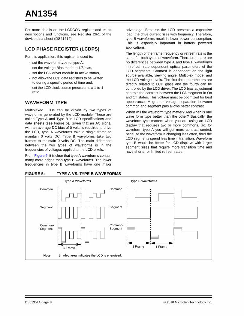
WAVEFORM TYPE
Multiplexed LCDs can be driven by two types ofwaveforms generated by the LCD module. These arecalled Type A and Type B in LCD specifications anddata sheets (see Figure 5). Given that an AC signalwith an average DC bias of 0 volts is required to drivethe LCD, type A waveforms take a single frame tomaintain 0 volts DC. Type B waveforms take twoframes to maintain 0 volts DC. The main differencebetween the two types of waveforms is in thefrequencies of voltages applied to the LCD pixels.
From Figure 5, it is clear that type A waveforms containmany more edges than type B waveforms. The lowerfrequencies in type B waveforms have one major
advantage. Because the LCD presents a capacitiveload, the drive current rises with frequency. Therefore,type B waveforms result in lower power consumption.This is especially important in battery poweredapplications.
The length of the frame frequency or refresh rate is thesame for both types of waveform. Therefore, there areno differences between type A and type B waveformsin refresh rate dependent optical parameters of theLCD segments. Contrast is dependent on the lightsource available, viewing angle, Multiplex mode, andthe LCD voltage levels. The first three parameters aredirectly related to LCD glass and the fourth can becontrolled by the LCD driver. The LCD bias adjustmentcontrols the contrast between the LCD segment in Onand Off states. This voltage must be optimized for bestappearance. A greater voltage separation betweencommon and segment pins allows better contrast.
When will the waveform type matter? And when is onewave form type better than the other? Basically, thewaveform type matters when you are using an LCDdisplay that requires two or more commons. So, forwaveform type A you will get more contrast control,because the waveform is changing less often, thus theLCD segments spend less time in transition. Waveformtype B would be better for LCD displays with largersegment sizes that require more transition time andhave shorter or limited refresh rates.
FIGURE 5: TYPE A VS. TYPE B WAVEFORMS
Type A Waveforms Type B Waveforms
Common
Segment
Common-Segment
Common
Segment
Common-Segment
1 Frame 1 Frame
Note: Shaded area indicates the LCD is energized.
1 Frame
DS01354A-page 8 2010 Microchip Technology Inc.

AN1354
Voltage Bias
What does bias mean? Bias is the number of voltagesteps to be applied to the LCD. To control LCDs with alarger multiplex ratio, you must provide the waveformgenerator with multiple bias voltage level points. Theresulting waveform sent to the LCD segment controllines and backplane/commons contains a stair-steppedwaveform. This maintains specific AC voltages acrossany given segment, dot, and pixel to keep it in its On orOff state. The LCD bias number (for example, 1/3 bias)indicates how many voltage reference points are cre-ated to drive a specific LCD. Table 1 shows the relation-ship between the number of driving bias voltages andthe display multiplex ratios typically used.
For the PIC16F1947 microcontroller, the LCD modulecan be configured for one of three bias types:
a) Static Bias (2 voltage levels: VSS and VLCD)
b) 1/2 Bias (3 voltage levels: VSS, 1/2 VLCD andVLCD)
c) 1/3 Bias (4 voltage levels: VSS, 1/3 VLCD, 2/3VLCD and VLCD)
Being that the microcontroller and LCD used in thisapplication are configured for a 1/4 multiplex, the Biasmode will be set to 1/3 bias. This will give you thelowest possible LCD voltage, 1/3 VDD.
Frame Frequency
The LCD prescaler lets you divide the clockfrequencies to set the LCD frame clock rate which willallow us to adjust the frame frequency. The framefrequency is the rate at which the backplane orcommon and the segment outputs of the LCD change,this may also be called ‘Refresh Rate’. The range offrame frequencies is from 25 to 250 Hz with the mostcommon being between 50 and 150 Hz. The higherfrequencies result in higher power consumption, whilelower frequencies cause flicker in the image on theLCD panel. Figure 6 shows the LCD clock generationpath used to set the frame frequency. Table 4 showsFigure 6 in equations form for each multiplexconfiguration. Table 5 gives frame frequencies forseveral LCD prescaler values.
For more details on the LCDPS register and its bitdescriptions and functions, see Register 27-2 of thePIC16F1947 device data sheet (DS41414).
FIGURE 6: LCD CLOCK GENERATION
TABLE 4: FRAME FREQUENCY CALCULATION
TABLE 5: FRAME FREQUENCIES FOR DIFFERENT PRESCALER VALUES
1/3
1/4
Static
1/2 4-bit ProgPrescaler
+ 32Counter
+ 1, 2, 3, 4Ring Counter
+256Fosc
T1OSC 32 kHzCrystal Osc.
LFINTOSCNominal = 31 kHz
CS<1:0>LMUX<1:0>
+4
+2
To LadderPower Control
Segment
Clock
LP<3:0>
CO
M0
CO
M1
CO
M2
CO
M3
Multiplex Frame Frequency =
Static Clock source/(4x1x(LCD Prescaler)x32))
1/2 Clock source/(2x2x(LCD Prescaler)x32))
1/3 Clock source/(1x3x(LCD Prescaler)x32))
1/4 Clock source/(1x4x(LCD Prescaler)x32))
LP<3:0> Static 1/2 1/3 1/4
2 122 122 162 122
3 81 81 108 81
4 61 61 81 61
5 49 49 65 49
6 41 41 54 41
7 35 35 47 35
2010 Microchip Technology Inc. DS01354A-page 9
AN1354
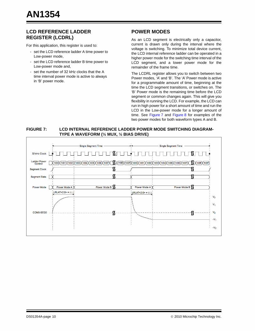
LCD REFERENCE LADDER REGISTER (LCDRL)
For this application, this register is used to:
- set the LCD reference ladder A time power to Low-power mode,
- set the LCD reference ladder B time power to Low-power mode and,
- set the number of 32 kHz clocks that the A time interval power mode is active to always in ‘B’ power mode.
POWER MODES
As an LCD segment is electrically only a capacitor,current is drawn only during the interval where thevoltage is switching. To minimize total device current,the LCD internal reference ladder can be operated in ahigher power mode for the switching time interval of theLCD segment, and a lower power mode for theremainder of the frame time.
The LCDRL register allows you to switch between twoPower modes, ‘A’ and ‘B’. The ‘A’ Power mode is activefor a programmable amount of time, beginning at thetime the LCD segment transitions, or switches on. The‘B’ Power mode is the remaining time before the LCDsegment or common changes again. This will give youflexibility in running the LCD. For example, the LCD canrun in high power for a short amount of time and run theLCD in the Low-power mode for a longer amount oftime. See Figure 7 and Figure 8 for examples of thetwo power modes for both waveform types A and B.
FIGURE 7: LCD INTERNAL REFERENCE LADDER POWER MODE SWITCHING DIAGRAM- TYPE A WAVEFORM (½ MUX, ½ BIAS DRIVE)
DS01354A-page 10 2010 Microchip Technology Inc.

AN1354
FIGURE 8: LCD INTERNAL REFERENCE LADDER POWER MODE SWITCHING DIAGRAM- TYPE B WAVEFORM (½ MUX, ½ BIAS DRIVE)
The internal reference ladder may operate in one ofthree power modes. The three different power modesare; Low, Medium and High. One power mode is notany better than the others for all microcontrollers. Thebest power mode for a given microcontroller and/orapplication will be dependent upon temperature, boardleakage, LCD leakage, capacitance of LCD, and yourunderstanding/preference of an acceptable contrastlevel. Thus, it allows you to trade off LCD contrast forpower in a specific application. The larger the LCDglass, the more capacitance is present on a physicalLCD segment, thus requiring more current to maintainthe same contrast level. The internal reference laddercan also be disconnected for applications that wish toprovide an external ladder or to minimize powerconsumption.
For more details on the LCDRL register and its bitdescriptions and functions, see Register 27-7 of thePIC16F1947 device data sheet (DS41414).
LCD CONTRAST CONTROL REGISTER (LCDCST)
For this application, this register is used to:
- set the LCD contrast resistance to the minimum resistance (i.e., the resistor ladder is shorted). (Therefore, the maximum con-trast, where the LCD segments are at their darkest).
FIGURE 9: CONTRAST CONTROL CIRCUIT
R R R RVDDIO
3.072V
From FVRBuffer
Internal Reference Contrast Control
LCDCST<2:0>
7 Stages
To Top ofReference Ladder
2010 Microchip Technology Inc. DS01354A-page 11

AN1354
Contrast Control
The contrast control circuit is used to decrease theoutput voltage of the signal source by a total ofapproximately 10%, thus the 7-stage resistor ladder isat maximum resistance (minimum contrast), thereforethe LCD segments are at their lightest. Likewise, whenyou increase the output voltage, the 7-stage resistorladder is at its minimum resistance (maximumcontrast), thus the LCD segments are at their darkest.
So, to save power, you will want to find a contrastsetting that will give you enough resistance to see theLCD segments, but does not use maximum voltage.However, keep in mind that the contrast can and will beaffected by the temperature of the LCD display glass,for example, the environmental temperature the displayis in. Also, you can set up the LCD to use an externalcontrast control circuit using pulse-width modulation(PWM). This gives you the option of having a largercontrast range (more than 10%) at a faster rate. SeeFigure 10 for an example of an external contrast controlcircuit using the pulse-width modulation (PWM)peripheral of the PIC16F1947 microcontroller.
FIGURE 10: EXTERNAL CONTRAST CONTROL CIRCUIT EXAMPLE
For more details on the LCDCST register and its bitdescriptions and functions, see Register 27-4 of thePIC16F1947 device data sheet (DS41414).
LCD REFERENCE VOLTAGE CONTROL REGISTER (LCDREF)
For this application, this register is used to:
- set the LCD internal voltage reference on (thus connecting to the internal contrast control circuit),
- set the internal contrast control to be powered by VDD,
- set the internal voltage reference ladder to allow the Fixed Voltage Reference (FVR) to shut down when the LCD voltage reference ladder is in power mode ‘B’,
- disconnect the LCD voltage pins from the bias voltage generator
This register gives you the option of two differentvoltage references to drive the LCD and contrastcontrol circuit. You can select from VDD or the internalFixed Voltage Reference, as shown in Figure 11. Thiswill allow you to drive a 5V LCD or a 3V LCD display,but only if the microcontroller is running at 5 volts. If themicrocontroller is running at 3 volts, you would only beable to run a 3-volt LCD display.
VLCD3CCP1
DS01354A-page 12 2010 Microchip Technology Inc.

AN1354
FIGURE 11: LCD BIAS VOLTAGE GENERATOR BLOCK DIAGRAM
The block diagram in Figure 11 can also be modifiedusing external capacitors to reduce powerconsumption. By putting external capacitors on theVLCD3, 2 and 1 pins, the capacitors will charge up whenthe LCD is not being used and will discharge when theLCD is in use. Thus, reducing the amount of currentneeded from the resister ladder and allowing you toturn the ladder off. For an example of this modification,see Figure 12.
For more details on the LCDREF register and its bitdescriptions and functions, see Register 27-3 of thePIC16F1947 device data sheet (DS41414).
FIGURE 12: EXTERNAL CAPACITOR CIRCUIT EXAMPLE
LCD SEGMENT ENABLE REGISTERS (LCDSen)
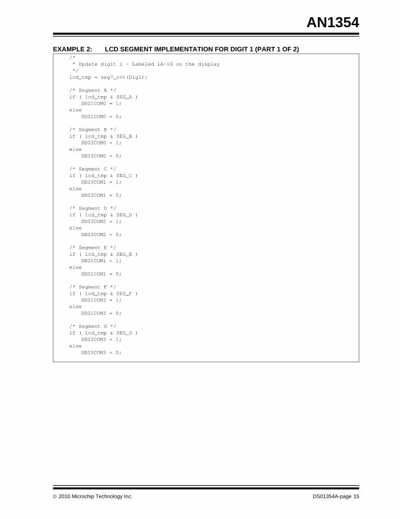
For this application, this register is used to enable/turnon all LCD segments that you will be using. Looking atsource code Example 1, all of the LCDSEn registershave all segment bits associated to their correspondingLCDDATAn register bits set to ‘1’ . This will enable allof the LCD display segments associated with theseregisters. Thus, the LCD source code shown in sourcecode Example 2 and in the complete application sourcecode shown in “Appendix A – Complete SourceCode”, will be able to turn on each LCD displaysegment as or when needed by the main program.
See Section “Segment Mapping” and source codeExample 1.
VLCD3
VLCD3PE
VLCD2
VLCD2PE
VLCD1
VLCD1PE
VDD
1.024V fromFVR
x33.072V
LCDIRELCDIRSLCDA
LCDIRELCDIRSLCDA
LCDA
LCDCST<2:>
BIASMD
lcdbias3
lcdbias2
lcdbias1
lcdbias0
A
B2
2
2
Power Mode Switching(LRLAP or LRLBP)
VLCD3
1µ
VLCD2
1µ
VLCD1
1µ
2010 Microchip Technology Inc. DS01354A-page 13
AN1354
LCD DATA REGISTERS (LCDDATAn)
For this application, this register is used to make all ofthe LCD segments either dark or clear as needed whilethe program is running. As you look at source codeExample 1, you will notice that all of the LCDDATAnregisters are set to ‘0’. This will turn all of the LCDdisplay segments associated with these registers off.The LCD source code shown in source codeExample 2 and in the complete application source codeshown in “Appendix A – Complete Source Code”,will turn on (set to ‘1’) each LCD display segment as orwhen needed by the main program.
For more details on the LCDDATAn register and its bitdescriptions and functions, see Register 27-6 of thePIC16F1947 device data sheet (DS41414).
Tying It All Together.
When you have gone through and determined whichLCD display segments you want to drive, whichmicrocontroller LCD segments will drive them, and howyou want to configure the LCD module, you need to tiethe source code to the application.
For the source code used in this application example,you do not need to use all segments of the LCD display.You need only to use digits 1 through 5 as shown in theLCD segment mapping worksheet, see Table 2. Forsimplicity purposes, the source code has been writtento automatically use these digits as needed. See codeExample 2.
THE APPLICATION
The example application for this document is anelectronic combination lock. It works as follows:
Select a 3-digit code – for example: 4, 5, 6.
- Push button 1:
This button lets you select a number from 0 to 9.Thus, as you press the button, the LCD will dis-play numbers incrementing from 0 to 9, thenback to 0, and so on.
- Push button 2:
This is the Enter button. So, when the LCD dis-plays the first number of the 3-digit code usingpush button 1, enter the number using push but-ton 2. Repeat this process until all 3 digits areentered, then the LCD will display “UNLOC”(Figure 1).
- Push button 3:
This is the Reset button. Press this button toreset the device.
- Push button 4:
This is the LCD contrast control. As you pressthis button, you will notice the brightness/contrast of the pixels get lighter and lighter, thenback to maximum darkness.
See “Appendix A – Complete Source Code” for thecomplete source code and schematic used in thisapplication.
DS01354A-page 14 2010 Microchip Technology Inc.
AN1354
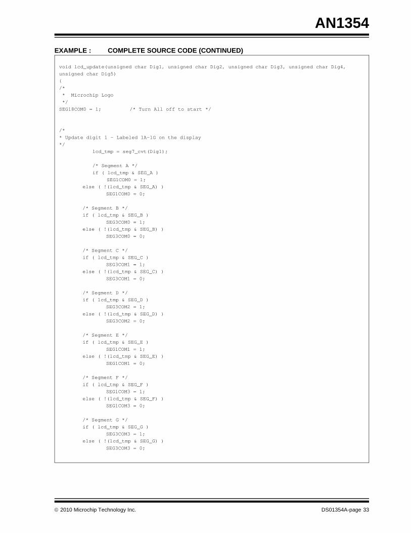
EXAMPLE 2: LCD SEGMENT IMPLEMENTATION FOR DIGIT 1 (PART 1 OF 2)/* * Update digit 1 - Labeled 1A-1G on the display */lcd_tmp = seg7_cvt(Dig1);
/* Segment A */if ( lcd_tmp & SEG_A )
SEG1COM0 = 1;else
SEG1COM0 = 0;
/* Segment B */if ( lcd_tmp & SEG_B )
SEG3COM0 = 1;else
SEG3COM0 = 0;
/* Segment C */if ( lcd_tmp & SEG_C )
SEG3COM1 = 1;else
SEG3COM1 = 0;
/* Segment D */if ( lcd_tmp & SEG_D )
SEG3COM2 = 1;else
SEG3COM2 = 0;
/* Segment E */if ( lcd_tmp & SEG_E )
SEG1COM1 = 1;else
SEG1COM1 = 0;
/* Segment F */if ( lcd_tmp & SEG_F )
SEG1COM3 = 1;else
SEG1COM3 = 0;
/* Segment G */if ( lcd_tmp & SEG_G )
SEG3COM3 = 1;else
SEG3COM3 = 0;
2010 Microchip Technology Inc. DS01354A-page 15

AN1354
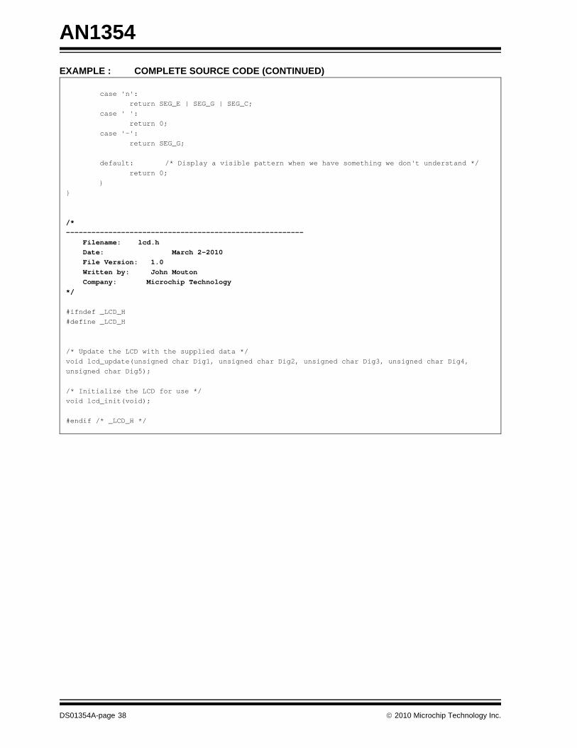
EXAMPLE 2: LCD SEGMENT IMPLEMENTATION FOR DIGIT 1 (PART 2 OF 2)/* Convert the integer value to which segments need to be turned on or off */unsigned char seg7_cvt(unsigned char digit){
switch (digit) {
case '0':case 0:
return SEG_A | SEG_B | SEG_C | SEG_D | SEG_E | SEG_F;case '1':case 1:
return SEG_B | SEG_C;case '2':case 2:
return SEG_A | SEG_B | SEG_D | SEG_E | SEG_G;case '3':case 3:
return SEG_A | SEG_B | SEG_C | SEG_D | SEG_G;case '4':case 4:
return SEG_B | SEG_C | SEG_F | SEG_G;case '5':case 5:
return SEG_A | SEG_C | SEG_D | SEG_F | SEG_G;case '6':case 6:
return SEG_A | SEG_C | SEG_D | SEG_E | SEG_F | SEG_G;case '7':case 7:
return SEG_A | SEG_B | SEG_C;case '8':case 8:
return SEG_A | SEG_B | SEG_C | SEG_D | SEG_E | SEG_F | SEG_G;case '9':case 9:
return SEG_A | SEG_B | SEG_C | SEG_D | SEG_F | SEG_G;case 'L':
return SEG_F | SEG_E | SEG_D;case 'O':
return SEG_A | SEG_B | SEG_C | SEG_D | SEG_E | SEG_F;case 'C':
return SEG_A | SEG_F | SEG_E | SEG_D;case 'U':
return SEG_F | SEG_E | SEG_D | SEG_C | SEG_B;case 'n':
return SEG_E | SEG_G | SEG_C;case ' ':
return 0;case '-':
return SEG_G;
default: /* Display a visible pattern when we have something we don't understand */ return 0; }}
DS01354A-page 16 2010 Microchip Technology Inc.

AN1354
CONCLUSION
The PIC16F1947 microcontroller is ideally suited forLCD applications such as clocks, meters, thermostats,etc. This application note describes how to configure/optimize the LCD module for low-power consumptionand implement it in a real world application.Nevertheless, the configurations discussed will bemore dependent on the application and the LCDdisplay used. However, if you optimize your sourcecode to take advantage of the Sleep mode wheneverpossible, optimize the LCD module settings to find theperfect balance of contrast vs. power consumption anduse good power, ground and noise techniques whendesigning your applications’ circuit, you will be well onyour way to maximizing the LCD module ofPIC16F1947 microcontroller and its features toenhance any application.
Please refer to application note AN658, “LCDFundamentals using the PIC16C92X Microcontrollers”,for a more detailed discussion on how LCD displaysare constructed.
2010 Microchip Technology Inc. DS01354A-page 17

AN1354
NOTES:
DS01354A-page 18 2010 Microchip Technology Inc.
AN1354
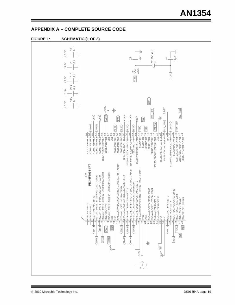
APPENDIX A – COMPLETE SOURCE CODE
FIGURE 1: SCHEMATIC (1 OF 3)
PIC16F1974-I/PT
U2
kHz
2010 Microchip Technology Inc. DS01354A-page 19
AN1354
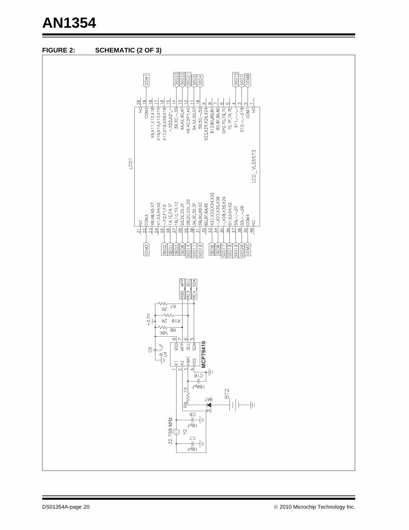
FIGURE 2: SCHEMATIC (2 OF 3)
MCP79410
kHz
DS01354A-page 20 2010 Microchip Technology Inc.

AN1354
FIGURE 3: SCHEMATIC (3 OF 3)
PIC
kit™
2
2010 Microchip Technology Inc. DS01354A-page 21

AN1354
EXAMPLE : COMPLETE SOURCE CODE/*
-------------------------------------------------------- Filename: 1947comboLoc.c Date: March 2-2010
File Version: 1.0 Written by: John Mouton
Company: Microchip Technology Files required: pic.h, LCD.c, and lcd.h
*/
#include <htc.h>#include "lcd.h"
// Setup the configuration word for use with ICD2
__CONFIG(FOSC_INTOSC & WDTE_OFF & MCLRE_ON & PWRTE_ON & BOREN_ON & IESO_OFF & FCMEN_OFF & CP_OFF & CPD_OFF & CLKOUTEN_OFF);
__CONFIG(WRT_OFF & VCAPEN_OFF & PLLEN_OFF & STVREN_ON & DEBUG_OFF & LVP_OFF & BORV_19);
static unsigned charCombination_Number_Flag = 0;// Combonation number flag.
// Combination Codestatic unsigned charCombination_Digit_1 = 4; //### You select this value. #####
static unsigned charCombination_Digit_2 = 5; //### You select this value. #####static unsigned charCombination_Digit_3 = 6; //### You select this value. #####
// Declarationsstatic unsigned char NUMBER_SELECT_BUTTON = 0; // flag indicating that SW1 was pressed.
static unsigned char ENTER_BUTTON = 0; // flag indicating that SW2 was pressed.static unsigned char RESET_BUTTON = 0; // flag indicating that SW3 was pressed.static unsigned char CONTRAST_CONTROL_BUTTON = 0; // flag indicating that SW4 was pressed.
static unsigned char state_variable = 0; // state counter variable.
static unsigned char Number_select_button_counter = 0; // counter variable for NUM_SELECT flag in
debounce subroutine.static unsigned char Enter_button_counter = 0; // counter variable for ENTER flag in
debounce subroutine.static unsigned char Reset_button_counter = 0; // counter variable for RESET flag in
debounce subroutine.
static unsigned char Contrast_Control_button_counter = 0; // counter variable for CONTRAST_CONTROL flag in debounce subroutine.
static unsigned char Number_selection_counter = 0; // counter variable for Decide_1 function.static unsigned char Decide_1_function_state_variable = 0; // state machine count variable for
Decide_1 function.
static unsigned char Decide_4_function_state_variable = 0; // state machine count variable for Decide_4 function.
static unsigned char Decide1_output_flag = 0; // output flag variable for Decide_1 function.
static unsigned char Decide2_output_flag = 0; // output flag variable for Decide_2
function.static unsigned char Decide3_output_flag = 0; // output flag variable for Decide_3
function.static unsigned char Decide4_output_flag = 0; // output flag variable for Decide_4
function.
DS01354A-page 22 2010 Microchip Technology Inc.

AN1354
EXAMPLE : COMPLETE SOURCE CODE (CONTINUED)
unsigned long int Interrupt_count = 0; // 32 bit interrupt counter variablestatic unsigned char lockup_flag; // interrupt variable to lockup
the device if interrup occures.
// function prototype
void INIT(void); // device initialization function.void GET_inputs(void); // recieve all inputs function.void Decide_1(void); // based on inputs, select a number function.
void Decide_2(void); // based on inputs, check/verify number selection function.void Decide_3(void); // based on inputs, check/verify reset function.
void Decide_4(void); // based on inputs, check/verify contrast control selection function.void DO_outputs(void); // based on decisions, display proper outputs function.
void leds_on(void); // sub-fuction of DO_out function to turn LEDs on.void leds_off(void); // sub-fuction of DO_out function to turn LEDs off.
void interrupt Time_out_int(void); // interrupt subroutine timeout function.
/*-----------------------------------------------------------------------------------Subroutine: INIT
Parameters: noneReturns:nothing
Synopsys:Initializes flags, and variables, sets PORT direction,configures analog/digital pins, and disables the comparator module
-----------------------------------------------------------------------------------*/
void INIT(void) {
TRISA = 0b11000000; // set port A as outputs. TRISB = 0b11000000; // set port B bits 4,5,6,7 as outputs and RB0,1,2,3 as inputs. TRISC = 0x00; // set port C as outputs.
TRISD = 0x00; // set port D as outputs. TRISE = 0x00; // set port E as outputs.
TRISF = 0x00; TRISG = 0x00;
ANSELA = 0x00; // make all analog outputs.
ANSELE = 0x00; // make all analog outputs. ANSELF = 0x00;
ANSELG = 0x00;
LATA = 0x00;
LATB = 0x00; LATC = 0x00; LATD = 0x00;
LATE = 0x00; LATF = 0x00;
LATG = 0x00;
CM1CON0 = 0x07; // turn off the comparators. CM2CON0 = 0x07;
CM1CON1 = 0x07; CM2CON1 = 0x07;
OPTION_REG = 0x00; // clear the OPTION_REG. INTCON = 0xA0; // enable peripheral interrupts
TMR0 = 0; // clear timer 0. RD4 = 0; // set RD4 to 0. RB7 = 0;
PORTA = 0; // CLEAR ALL PORTS, variables, and flags. PORTB = 0;
PORTC = 0; PORTD = 0; PORTE = 0;
PORTF = 0; PORTG = 0;
2010 Microchip Technology Inc. DS01354A-page 23

AN1354
EXAMPLE : COMPLETE SOURCE CODE (CONTINUED)
// Initialize variables
Number_select_button_counter = 0;
Enter_button_counter = 0; Reset_button_counter = 0;
Contrast_Control_button_counter = 0; Number_selection_counter = 0; Decide_1_function_state_variable = 0;
Decide_4_function_state_variable = 0; NUMBER_SELECT_BUTTON = 0;
ENTER_BUTTON = 0; RESET_BUTTON = 0; CONTRAST_CONTROL_BUTTON = 0;
Combination_Number_Flag = 0; Decide1_output_flag = 0;
Decide2_output_flag = 0; Decide3_output_flag = 0; Decide4_output_flag = 0;
// Initialize your combination value here.
Combination_Digit_1 = 4; // ### You select this value. #####
Combination_Digit_2 = 5; // ### You select this value. ##### Combination_Digit_3 = 6; // ### You select this value. #####
// Initializing the Interrupt routine variables. Interrupt_count = 0; // clear interrupt counter.
lockup_flag = 0; // clear interrupt lockup flag.
// Set up the LCD for use
lcd_init(); // calls the lcd initialization function. SEG18COM0 = 1; // MCHP logo}
/*-----------------------------------------------------------------------------------Subroutine: main
Parameters: noneReturns:nothing
Synopsys:Main program function-----------------------------------------------------------------------------------*/
void main(void)
{INIT(); //Initialize all registers
while(1)
{GET_inputs(); //Get inputs from off-chipDecide_1(); //Make decisions based on inputs
Decide_2(); //Make decisions based on inputs Decide_3(); //Make decisions based on inputs for Reset
Decide_4(); //Make decisions based on inputs for Contrast ControlDO_outputs(); //Do outputs based on decisions}
}
/*-----------------------------------------------------------------------------------
Subroutine: GET_inputsParameters: noneReturns:nothing
Synopsys:Gets the inputs from buttons on Mechatronics Demo Board.-----------------------------------------------------------------------------------*/
DS01354A-page 24 2010 Microchip Technology Inc.

AN1354
EXAMPLE : COMPLETE SOURCE CODE (CONTINUED)void GET_inputs(void) {
// DEBOUNCE FUNCTION FOR SW1.
if (RB6 == 0) Number_select_button_counter++; // this routine eliminates the contact bounce of the SW1 button being pressed.
else Number_select_button_counter = 0;if (Number_select_button_counter >= 9) Number_select_button_counter = 9; // it looks for 8
consective lows before
if (Number_select_button_counter == 8) NUMBER_SELECT_BUTTON = 1; // it determines the button is pressed
// DEBOUNCE FUNCTION FOR SW2.
if (RB7 == 0) Enter_button_counter++; // this routine eliminates the contact bounce of the SW2 button being pressed.
else Enter_button_counter = 0;if (Enter_button_counter >= 9) Enter_button_counter = 9; // it looks for 8 consective lows
before
if (Enter_button_counter == 8) ENTER_BUTTON = 1; // it determines the button is pressed
// DEBOUNCE FUNCTION FOR SW3.
if (RA6 == 0) Reset_button_counter++; // this routine eliminates the contact bounce of the SW3 button being pressed.
else Reset_button_counter = 0;
if (Reset_button_counter >= 9) Reset_button_counter = 9; // it looks for 8 consective lows before
if (Reset_button_counter == 8) RESET_BUTTON = 1; // it determines the button is pressed
// DEBOUNCE FUNCTION FOR SW4.
if (RA7 == 0) Contrast_Control_button_counter++; // this routine eliminates the contact bounce
of the SW4 button being pressed.else Contrast_Control_button_counter = 0;if (Contrast_Control_button_counter >= 9) Contrast_Control_button_counter = 9; // it looks
for 8 consective lows beforeif (Contrast_Control_button_counter == 8) CONTRAST_CONTROL_BUTTON = 1; // it determines the
button is pressed
}
/*-----------------------------------------------------------------------------------Subroutine: Decide_1Parameters: none
Returns:nothingSynopsys:This function steps through numbers 0 - 9, then back to 0, each time
the user presses the SW2 button.-----------------------------------------------------------------------------------*/
void Decide_1(void) {
if (NUMBER_SELECT_BUTTON == 1) {
Decide1_output_flag = 1; NUMBER_SELECT_BUTTON = 0;
2010 Microchip Technology Inc. DS01354A-page 25

AN1354
EXAMPLE : COMPLETE SOURCE CODE (CONTINUED)
switch(Decide_1_function_state_variable){ // State machine for the number selection.
case 0: {
Number_selection_counter = 0; Combination_Number_Flag = Number_selection_counter; Decide_1_function_state_variable = 1;
} break;
case 1: {
Number_selection_counter = 1; Combination_Number_Flag = Number_selection_counter;
Decide_1_function_state_variable = 2;
}
break;
case 2: {
Number_selection_counter = 2; Combination_Number_Flag = Number_selection_counter; Decide_1_function_state_variable = 3;
}
break;
case 3:
{ Number_selection_counter = 3;
Combination_Number_Flag = Number_selection_counter;
Decide_1_function_state_variable = 4;
} break;
case 4: {
Number_selection_counter = 4; Combination_Number_Flag = Number_selection_counter;
Decide_1_function_state_variable = 5; }
break;
case 5: {
Number_selection_counter = 5; Combination_Number_Flag = Number_selection_counter;
Decide_1_function_state_variable = 6; }
break;
DS01354A-page 26 2010 Microchip Technology Inc.
AN1354
EXAMPLE : COMPLETE SOURCE CODE (CONTINUED) case 6:
{ Number_selection_counter = 6; Combination_Number_Flag = Number_selection_counter;
Decide_1_function_state_variable = 7;
} break;
case 7: {
Number_selection_counter = 7; Combination_Number_Flag = Number_selection_counter; Decide_1_function_state_variable = 8;
} break;
case 8: {
Number_selection_counter = 8; Combination_Number_Flag = Number_selection_counter;
Decide_1_function_state_variable = 9;
} break;
case 9: {
Number_selection_counter = 9; Combination_Number_Flag = Number_selection_counter;
Decide_1_function_state_variable = 0; }
break;
default:
{ Decide_1_function_state_variable = 0;
} break;
} }
}
/*-----------------------------------------------------------------------------------
Subroutine: Decide_2Parameters: none
Returns:nothingSynopsys:This function will check the numbers selected and entered as the three
digit code to unlock the electronic lock.-----------------------------------------------------------------------------------*/
void Decide_2(void) {
if (ENTER_BUTTON == 1) { Decide2_output_flag = 1;
ENTER_BUTTON =0; switch(state_variable){
2010 Microchip Technology Inc. DS01354A-page 27
AN1354
EXAMPLE : COMPLETE SOURCE CODE (CONTINUED) case 0:
if (Combination_Number_Flag == Combination_Digit_1) // checks the first number entered of the three digit combo.
{
state_variable = 1; // increments state variable Decide_1_function_state_variable = 0;
} else {
state_variable = 0; Decide_1_function_state_variable = 0;
} break;
case 1: if (Combination_Number_Flag == Combination_Digit_2) // checks the second
number entered of the three digit combo.
{ state_variable = 2; // increments state variable
Decide_1_function_state_variable = 0; }
else { state_variable = 0;
Decide_1_function_state_variable = 0; }
break;
case 2:
if (Combination_Number_Flag == Combination_Digit_3) // checks the third number entered of the three digit combo.
{
state_variable = 3; // increments state variable, thus when the state variable
// equals 3, the entire three digit combo is verified correct.
Decide_1_function_state_variable = 0;
} else
{ state_variable = 0; Decide_1_function_state_variable = 0;
} break;
case 3:
{ state_variable = 0; Decide_1_function_state_variable = 0;
} break;
default: // default case.
{ state_variable = 0; Decide_1_function_state_variable = 0;
} break;
}
}
}
DS01354A-page 28 2010 Microchip Technology Inc.
AN1354
EXAMPLE : COMPLETE SOURCE CODE (CONTINUED)/*-----------------------------------------------------------------------------------
Subroutine: Decide_3Parameters: noneReturns:nothing
Synopsys:This function will monitor SW3 and if it is pressed, the demo will reset.-----------------------------------------------------------------------------------*/
void Decide_3(void) {
if (RESET_BUTTON == 1) {
Decide3_output_flag = 1; RESET_BUTTON =0; INIT();
}
}
/*-----------------------------------------------------------------------------------
Subroutine: Decide_4Parameters: none
Returns:nothingSynopsys:This function will change the brightness of the LCD digits.
-----------------------------------------------------------------------------------*/
void Decide_4(void) {
if (CONTRAST_CONTROL_BUTTON == 1) {
Decide4_output_flag = 1; LCDCST++;
CONTRAST_CONTROL_BUTTON =0; }
}
/*-----------------------------------------------------------------------------------Subroutine: DO_out
Parameters: noneReturns:nothing
Synopsys:This function will display Locked or unlocked based on the outputs of the decision functions.
-----------------------------------------------------------------------------------*/
void DO_outputs(void) {
if (lockup_flag == 1 ) // if the interrupt lockup flag is set, // dashed lines will appear on the LCD
{ lcd_update ('-','-','-','-','-'); }
else
{ if(Decide1_output_flag == 1 && Decide2_output_flag == 0 ) // if SW2 is pressed but SW3 isn't,
then display the // current number value. {
Decide1_output_flag = 0; lcd_update (' ',' ',' ',' ',Number_selection_counter);
}
2010 Microchip Technology Inc. DS01354A-page 29

AN1354
EXAMPLE : COMPLETE SOURCE CODE (CONTINUED)
else if(Decide1_output_flag == 0 && Decide2_output_flag == 1) // If SW2 was pressed and the number value you want is etered ( via SW3 )and it is correct. Then display unlocked, if not display locked.
{ Decide1_output_flag = 0;
Decide2_output_flag = 0;
if ( state_variable == 3 )
{ RB7 = 1;
lcd_update ('U','n','L','O','C'); Interrupt_count = 0; // The interrupt counter will reset. lockup_flag = 0; // The interrupt lockup flag will reset.
TMR0IE = 0; // The timer 0 enable bit will turn off so the // interrupt routine will not time out even if
// the electronic combo lock is unlocked. }
else {
lcd_update (' ','L','O','C',' '); RB7 = 0;
} }
else {
Decide1_output_flag = 0; Decide2_output_flag = 0; }
}
}
/*-----------------------------------------------------------------------------------Subroutine: Time_out_int
Parameters: noneReturns:nothing
Synopsys:This is the interrupt function that will lock you out of the electronic combination lock if you don't enter the correct 3 digit combination fast enough.
-----------------------------------------------------------------------------------*/
void interrupt Time_out_int(void) {
if (TMR0IF == 1 ) // If the Timer 0 interrupt flag is set,
{ // increment the interrupt counter and Interrupt_count ++ ; // clear the Timer 0 interrupt flag.
TMR0IF = 0; }
if (Interrupt_count == 30000 ) // If the interrupt counter is equal to 30000, { // set the lockup flag.
lockup_flag = 1; }
}
/*
DS01354A-page 30 2010 Microchip Technology Inc.

AN1354
EXAMPLE : COMPLETE SOURCE CODE (CONTINUED)
********************************************************************************** CODE OWNERSHIP AND DISCLAIMER OF LIABILITY
*
* Microchip Technology Incorporated ("Microchip") retains all ownership and * intellectual property rights in the code accompanying this message and in all * derivatives hereto. You may use this code, and any derivatives created by
* any person or entity by or on your behalf, exclusively with Microchip’s * proprietary products. Your acceptance and/or use of this code constitutes
* agreement to the terms and conditions of this notice. * * CODE ACCOMPANYING THIS MESSAGE IS SUPPLIED BY MICROCHIP "AS IS". NO
* WARRANTIES, WHETHER EXPRESS, IMPLIED OR STATUTORY, INCLUDING, BUT NOT LIMITED * TO, IMPLIED WARRANTIES OF NON-INFRINGEMENT, MERCHANTABILITY AND FITNESS FOR A
* PARTICULAR PURPOSE APPLY TO THIS CODE, ITS INTERACTION WITH MICROCHIP’S * PRODUCTS,COMBINATION WITH ANY OTHER PRODUCTS, OR USE IN ANY APPLICATION. *
* YOU ACKNOWLEDGE AND AGREE THAT, IN NO EVENT, SHALL MICROCHIP BE LIABLE, * WHETHER IN CONTRACT, WARRANTY, TORT (INCLUDING NEGLIGENCE OR BREACH OF
* STATUTORY DUTY), STRICT LIABILITY, INDEMNITY,CONTRIBUTION, OR OTHERWISE, FOR * ANY INDIRECT, SPECIAL, PUNITIVE, EXEMPLARY, INCIDENTAL OR CONSEQUENTIAL LOSS,
* DAMAGE, FOR COST OR EXPENSE OF ANY KIND WHATSOEVER RELATED TO THE CODE, * HOWSOEVER CAUSED, EVEN IF MICROCHIP HAS BEEN ADVISED OF THE POSSIBILITY OR * THE DAMAGES ARE FORESEEABLE. TO THE FULLEST EXTENT ALLOWABLE BY LAW,
* MICROCHIP'S TOTAL LIABILITY ON ALL CLAIMS IN ANY WAY RELATED* TO THIS CODE, * SHALL NOT EXCEED THE PRICE YOU PAID DIRECTLY TO MICROCHIP SPECIFICALLY TO
* HAVE THIS CODE DEVELOPED. * * You agree that you are solely responsible for testing the code and
* determining its suitability. Microchip has no obligation to modify, test, * certify, or support the code.
*********************************************************************************/
/*--------------------------------------------------------
Filename: LCD.c Date: March 2-2010 File Version: 1.0
Written by: John Mouton Company: Microchip Technology
*/
#include <pic.h>
#include "lcd.h"
//Function Prototypevoid lcd_update(unsigned char Dig1, unsigned char Dig2 , unsigned char Dig3, unsigned char Dig4, unsigned char Dig5);
/*
* Update the LCD with the supplied numerical values * * Note that we use two back to back if statements when comparing bits rather
* than if-else as it is smaller */
2010 Microchip Technology Inc. DS01354A-page 31
AN1354
EXAMPLE : COMPLETE SOURCE CODE (CONTINUED)
/* Segments in a 7 segment display */#define SEG_A 0x01#define SEG_B 0x02
#define SEG_C 0x04#define SEG_D 0x08
#define SEG_E 0x10#define SEG_F 0x20#define SEG_G 0x40
static bank1 unsigned char lcd_tmp;
unsigned char seg7_cvt(unsigned char digit);
void lcd_init(void){
LCDSE0 = 0xFE; // enable first group of LCD segment outputs LCDSE1 = 0x8F; // enable second group of LCD segments LCDSE2 = 0xFF; // enable third group of LCD segments
LCDSE3 = 0x00; LCDSE4 = 0x00;
LCDSE5 = 0x00; LCDDATA0 = 0; // clear LCD segment registers
LCDDATA1 = 0; LCDDATA2 = 0; LCDDATA3 = 0;
LCDDATA4 = 0; LCDDATA5 = 0;
LCDDATA6 = 0; LCDDATA7 = 0; LCDDATA8 = 0;
LCDDATA9 = 0; LCDDATA10 = 0;
LCDDATA11 = 0; LCDDATA12 = 0; LCDDATA13 = 0;
LCDDATA14 = 0; LCDDATA15 = 0;
LCDDATA16 = 0; LCDDATA17 = 0; LCDDATA18 = 0;
LCDDATA19 = 0; LCDDATA20 = 0;
LCDDATA21 = 0; LCDDATA22 = 0; LCDDATA23 = 0;
// WAVEFORM TYPE A, LCD MODULE IS ACTIVE
LCDPS = 0x20; // PRESCALER IS 1:1, BIAS IS 0 (CAN BE STATIC OR 1/3) // LCD MODULE IS ON, DRIVER MODULE IS ENABLED DURING SLEEP
LCDCON = 0x8B; // NO WRITE FAIL ERROR, VLDC PINS ARE ENABLED, MULTIPLEX 1/4 BIAS 1/3 LCDREF = 0x80;
LCDCST = 0x00; LCDRL = 0xF0;
}
DS01354A-page 32 2010 Microchip Technology Inc.
AN1354
EXAMPLE : COMPLETE SOURCE CODE (CONTINUED)
void lcd_update(unsigned char Dig1, unsigned char Dig2, unsigned char Dig3, unsigned char Dig4, unsigned char Dig5){
/* * Microchip Logo
*/SEG18COM0 = 1; /* Turn All off to start */
/*
* Update digit 1 - Labeled 1A-1G on the display*/ lcd_tmp = seg7_cvt(Dig1);
/* Segment A */
if ( lcd_tmp & SEG_A ) SEG1COM0 = 1;else ( !(lcd_tmp & SEG_A) )
SEG1COM0 = 0;
/* Segment B */if ( lcd_tmp & SEG_B )
SEG3COM0 = 1;else ( !(lcd_tmp & SEG_B) )
SEG3COM0 = 0;
/* Segment C */
if ( lcd_tmp & SEG_C )SEG3COM1 = 1;
else ( !(lcd_tmp & SEG_C) )
SEG3COM1 = 0;
/* Segment D */if ( lcd_tmp & SEG_D )
SEG3COM2 = 1;
else ( !(lcd_tmp & SEG_D) )SEG3COM2 = 0;
/* Segment E */if ( lcd_tmp & SEG_E )
SEG1COM1 = 1;else ( !(lcd_tmp & SEG_E) )
SEG1COM1 = 0;
/* Segment F */
if ( lcd_tmp & SEG_F )SEG1COM3 = 1;
else ( !(lcd_tmp & SEG_F) )SEG1COM3 = 0;
/* Segment G */if ( lcd_tmp & SEG_G )
SEG3COM3 = 1;else ( !(lcd_tmp & SEG_G) )
SEG3COM3 = 0;
2010 Microchip Technology Inc. DS01354A-page 33

AN1354
EXAMPLE : COMPLETE SOURCE CODE (CONTINUED)
/* * Update digit 2 - Labled 2A-2G on the display */
lcd_tmp = seg7_cvt(Dig2);
/* Segment A */if ( lcd_tmp & SEG_A )
SEG6COM0 = 1;
else ( !(lcd_tmp & SEG_A) )SEG6COM0 = 0;
/* Segment B */if ( lcd_tmp & SEG_B )
SEG16COM0 = 1;else ( !(lcd_tmp & SEG_B) )
SEG16COM0 = 0;
/* Segment C */
if ( lcd_tmp & SEG_C )SEG16COM1 = 1;
else ( !(lcd_tmp & SEG_C) )SEG16COM1 = 0;
/* Segment D */if ( lcd_tmp & SEG_D )
SEG6COM2 = 1;else ( !(lcd_tmp & SEG_D) )
SEG6COM2 = 0;
/* Segment E */
if ( lcd_tmp & SEG_E )SEG6COM1 = 1;
else ( !(lcd_tmp & SEG_E) )SEG6COM1 = 0;
/* Segment F */if ( lcd_tmp & SEG_F )
SEG6COM3 = 1;else ( !(lcd_tmp & SEG_F) )
SEG6COM3 = 0;
/* Segment G */
if ( lcd_tmp & SEG_G )SEG16COM3 = 1;
else ( !(lcd_tmp & SEG_G) )
SEG16COM3 = 0;
/* * Update digit 3 - Labled 3A-3G on the display
*/lcd_tmp = seg7_cvt(Dig3);
SEG22COM3 = 0;
/* Segment G */
if ( lcd_tmp & SEG_G )SEG21COM3 = 1;
else ( !(lcd_tmp & SEG_G) )
SEG21COM3 = 0;
DS01354A-page 34 2010 Microchip Technology Inc.

AN1354
EXAMPLE : COMPLETE SOURCE CODE (CONTINUED)
/* Segment A */if ( lcd_tmp & SEG_A )
SEG11COM0 = 1;
else ( !(lcd_tmp & SEG_A) )SEG11COM0 = 0;
/* Segment B */if ( lcd_tmp & SEG_B )
SEG23COM0 = 1;else ( !(lcd_tmp & SEG_B) )
SEG23COM0 = 0;
/* Segment C */
if ( lcd_tmp & SEG_C )SEG23COM1 = 1;
else ( !(lcd_tmp & SEG_C) )SEG23COM1 = 0;
/* Segment D */if ( lcd_tmp & SEG_D )
SEG11COM2 = 1;else ( !(lcd_tmp & SEG_D) )
SEG11COM2 = 0;
/* Segment E */
if ( lcd_tmp & SEG_E )SEG11COM1 = 1;
else ( !(lcd_tmp & SEG_E) )SEG11COM1 = 0;
/* Segment F */if ( lcd_tmp & SEG_F )
SEG11COM3 = 1;else ( !(lcd_tmp & SEG_F) )
SEG11COM3 = 0;
/* Segment G */
if ( lcd_tmp & SEG_G )SEG23COM3 = 1;
else ( !(lcd_tmp & SEG_G) )
SEG23COM3 = 0;
/* * Update digit 4 - Labeled 4A-4G on the display
*/lcd_tmp = seg7_cvt(Dig4);
/* Segment A */
if ( lcd_tmp & SEG_A )SEG22COM0 = 1;
else ( !(lcd_tmp & SEG_A) )
SEG22COM0 = 0;
/* Segment B */if ( lcd_tmp & SEG_B )
SEG21COM0 = 1;
else ( !(lcd_tmp & SEG_B) )SEG21COM0 = 0;
2010 Microchip Technology Inc. DS01354A-page 35

AN1354
EXAMPLE : COMPLETE SOURCE CODE (CONTINUED)
/* Segment C */if ( lcd_tmp & SEG_C )
SEG21COM1 = 1;
else ( !(lcd_tmp & SEG_C) )SEG21COM1 = 0;
/* Segment D */if ( lcd_tmp & SEG_D )
SEG22COM2 = 1;else ( !(lcd_tmp & SEG_D) )
SEG22COM2 = 0;
/* Segment E */
if ( lcd_tmp & SEG_E )SEG22COM1 = 1;
else ( !(lcd_tmp & SEG_E) )SEG22COM1 = 0;
/* Segment F */if ( lcd_tmp & SEG_F )
SEG22COM3 = 1;else ( !(lcd_tmp & SEG_F) )
/* * Update digit 5 - Labeled 5A-5G on the display
*/
lcd_tmp = seg7_cvt(Dig5);
/* Segment A */
if ( lcd_tmp & SEG_A )SEG5COM0 = 1;
else ( !(lcd_tmp & SEG_A) )SEG5COM0 = 0;
/* Segment B */if ( lcd_tmp & SEG_B )
SEG4COM0 = 1;else ( !(lcd_tmp & SEG_B) )
SEG4COM0 = 0;
/* Segment C */
if ( lcd_tmp & SEG_C )SEG4COM1 = 1;
else ( !(lcd_tmp & SEG_C) )
SEG4COM1 = 0;
/* Segment D */if ( lcd_tmp & SEG_D )
SEG5COM2 = 1;else ( !(lcd_tmp & SEG_D) )
SEG5COM2 = 0;
/* Segment E */
if ( lcd_tmp & SEG_E )SEG5COM1 = 1;
else ( !(lcd_tmp & SEG_E) )
SEG5COM1 = 0;
DS01354A-page 36 2010 Microchip Technology Inc.

AN1354
EXAMPLE : COMPLETE SOURCE CODE (CONTINUED)
/* Segment F */if ( lcd_tmp & SEG_F )
SEG5COM3 = 1;
else ( !(lcd_tmp & SEG_F) )SEG5COM3 = 0;
/* Segment G */if ( lcd_tmp & SEG_G )
SEG4COM3 = 1;else ( !(lcd_tmp & SEG_G) )
SEG4COM3 = 0;
}
/* Convert the integer value to which segments need to be turned on or off */
unsigned char seg7_cvt(unsigned char digit){ switch (digit)
{ case '0':
case 0: return SEG_A | SEG_B | SEG_C | SEG_D | SEG_E | SEG_F;
case '1': case 1:
return SEG_B | SEG_C;
case '2': case 2:
return SEG_A | SEG_B | SEG_D | SEG_E | SEG_G; case '3': case 3:
return SEG_A | SEG_B | SEG_C | SEG_D | SEG_G; case '4':
case 4: return SEG_B | SEG_C | SEG_F | SEG_G;
case '5':
case 5: return SEG_A | SEG_C | SEG_D | SEG_F | SEG_G;
case '6': case 6:
return SEG_A | SEG_C | SEG_D | SEG_E | SEG_F | SEG_G;
case '7': case 7:
return SEG_A | SEG_B | SEG_C; case '8': case 8:
return SEG_A | SEG_B | SEG_C | SEG_D | SEG_E | SEG_F | SEG_G; case '9':
case 9: return SEG_A | SEG_B | SEG_C | SEG_D | SEG_F | SEG_G;
case 'L': return SEG_F | SEG_E | SEG_D; case 'O':
return SEG_A | SEG_B | SEG_C | SEG_D | SEG_E | SEG_F; case 'C':
return SEG_A | SEG_F | SEG_E | SEG_D; case 'U': return SEG_F | SEG_E | SEG_D | SEG_C | SEG_B;
2010 Microchip Technology Inc. DS01354A-page 37
AN1354
EXAMPLE : COMPLETE SOURCE CODE (CONTINUED)
case 'n': return SEG_E | SEG_G | SEG_C; case ' ':
return 0; case '-':
return SEG_G; default: /* Display a visible pattern when we have something we don't understand */
return 0;}
}
/*--------------------------------------------------------
Filename: lcd.h Date: March 2-2010 File Version: 1.0
Written by: John Mouton Company: Microchip Technology
*/
#ifndef _LCD_H#define _LCD_H
/* Update the LCD with the supplied data */
void lcd_update(unsigned char Dig1, unsigned char Dig2, unsigned char Dig3, unsigned char Dig4, unsigned char Dig5);
/* Initialize the LCD for use */void lcd_init(void);
#endif /* _LCD_H */
DS01354A-page 38 2010 Microchip Technology Inc.

Note the following details of the code protection feature on Microchip devices:
• Microchip products meet the specification contained in their particular Microchip Data Sheet.
• Microchip believes that its family of products is one of the most secure families of its kind on the market today, when used in the intended manner and under normal conditions.
• There are dishonest and possibly illegal methods used to breach the code protection feature. All of these methods, to our knowledge, require using the Microchip products in a manner outside the operating specifications contained in Microchip’s Data Sheets. Most likely, the person doing so is engaged in theft of intellectual property.
• Microchip is willing to work with the customer who is concerned about the integrity of their code.
• Neither Microchip nor any other semiconductor manufacturer can guarantee the security of their code. Code protection does not mean that we are guaranteeing the product as “unbreakable.”
Code protection is constantly evolving. We at Microchip are committed to continuously improving the code protection features of ourproducts. Attempts to break Microchip’s code protection feature may be a violation of the Digital Millennium Copyright Act. If such actsallow unauthorized access to your software or other copyrighted work, you may have a right to sue for relief under that Act.
Information contained in this publication regarding deviceapplications and the like is provided only for your convenienceand may be superseded by updates. It is your responsibility toensure that your application meets with your specifications.MICROCHIP MAKES NO REPRESENTATIONS ORWARRANTIES OF ANY KIND WHETHER EXPRESS ORIMPLIED, WRITTEN OR ORAL, STATUTORY OROTHERWISE, RELATED TO THE INFORMATION,INCLUDING BUT NOT LIMITED TO ITS CONDITION,QUALITY, PERFORMANCE, MERCHANTABILITY ORFITNESS FOR PURPOSE. Microchip disclaims all liabilityarising from this information and its use. Use of Microchipdevices in life support and/or safety applications is entirely atthe buyer’s risk, and the buyer agrees to defend, indemnify andhold harmless Microchip from any and all damages, claims,suits, or expenses resulting from such use. No licenses areconveyed, implicitly or otherwise, under any Microchipintellectual property rights.
2010 Microchip Technology Inc.
Trademarks
The Microchip name and logo, the Microchip logo, dsPIC, KEELOQ, KEELOQ logo, MPLAB, PIC, PICmicro, PICSTART, PIC32 logo, rfPIC and UNI/O are registered trademarks of Microchip Technology Incorporated in the U.S.A. and other countries.
FilterLab, Hampshire, HI-TECH C, Linear Active Thermistor, MXDEV, MXLAB, SEEVAL and The Embedded Control Solutions Company are registered trademarks of Microchip Technology Incorporated in the U.S.A.
Analog-for-the-Digital Age, Application Maestro, CodeGuard, dsPICDEM, dsPICDEM.net, dsPICworks, dsSPEAK, ECAN, ECONOMONITOR, FanSense, HI-TIDE, In-Circuit Serial Programming, ICSP, Mindi, MiWi, MPASM, MPLAB Certified logo, MPLIB, MPLINK, mTouch, Omniscient Code Generation, PICC, PICC-18, PICDEM, PICDEM.net, PICkit, PICtail, REAL ICE, rfLAB, Select Mode, Total Endurance, TSHARC, UniWinDriver, WiperLock and ZENA are trademarks of Microchip Technology Incorporated in the U.S.A. and other countries.
SQTP is a service mark of Microchip Technology Incorporated in the U.S.A.
All other trademarks mentioned herein are property of their respective companies.
© 2010, Microchip Technology Incorporated, Printed in the U.S.A., All Rights Reserved.
Printed on recycled paper.
ISBN: 978-1-60932-534-3
DS01354A-page 39
Microchip received ISO/TS-16949:2002 certification for its worldwide headquarters, design and wafer fabrication facilities in Chandler and Tempe, Arizona; Gresham, Oregon and design centers in California and India. The Company’s quality system processes and procedures are for its PIC® MCUs and dsPIC® DSCs, KEELOQ® code hopping devices, Serial EEPROMs, microperipherals, nonvolatile memory and analog products. In addition, Microchip’s quality system for the design and manufacture of development systems is ISO 9001:2000 certified.

DS01354A-page 40 2010 Microchip Technology Inc.
AMERICASCorporate Office2355 West Chandler Blvd.Chandler, AZ 85224-6199Tel: 480-792-7200 Fax: 480-792-7277Technical Support: http://support.microchip.comWeb Address: www.microchip.com
AtlantaDuluth, GA Tel: 678-957-9614 Fax: 678-957-1455
BostonWestborough, MA Tel: 774-760-0087 Fax: 774-760-0088
ChicagoItasca, IL Tel: 630-285-0071 Fax: 630-285-0075
ClevelandIndependence, OH Tel: 216-447-0464 Fax: 216-447-0643
DallasAddison, TX Tel: 972-818-7423 Fax: 972-818-2924
DetroitFarmington Hills, MI Tel: 248-538-2250Fax: 248-538-2260
KokomoKokomo, IN Tel: 765-864-8360Fax: 765-864-8387
Los AngelesMission Viejo, CA Tel: 949-462-9523 Fax: 949-462-9608
Santa ClaraSanta Clara, CA Tel: 408-961-6444Fax: 408-961-6445
TorontoMississauga, Ontario, CanadaTel: 905-673-0699 Fax: 905-673-6509
ASIA/PACIFICAsia Pacific OfficeSuites 3707-14, 37th FloorTower 6, The GatewayHarbour City, KowloonHong KongTel: 852-2401-1200Fax: 852-2401-3431
Australia - SydneyTel: 61-2-9868-6733Fax: 61-2-9868-6755
China - BeijingTel: 86-10-8528-2100 Fax: 86-10-8528-2104
China - ChengduTel: 86-28-8665-5511Fax: 86-28-8665-7889
China - ChongqingTel: 86-23-8980-9588Fax: 86-23-8980-9500
China - Hong Kong SARTel: 852-2401-1200 Fax: 852-2401-3431
China - NanjingTel: 86-25-8473-2460Fax: 86-25-8473-2470
China - QingdaoTel: 86-532-8502-7355Fax: 86-532-8502-7205
China - ShanghaiTel: 86-21-5407-5533 Fax: 86-21-5407-5066
China - ShenyangTel: 86-24-2334-2829Fax: 86-24-2334-2393
China - ShenzhenTel: 86-755-8203-2660 Fax: 86-755-8203-1760
China - WuhanTel: 86-27-5980-5300Fax: 86-27-5980-5118
China - XianTel: 86-29-8833-7252Fax: 86-29-8833-7256
China - XiamenTel: 86-592-2388138 Fax: 86-592-2388130
China - ZhuhaiTel: 86-756-3210040 Fax: 86-756-3210049
ASIA/PACIFICIndia - BangaloreTel: 91-80-3090-4444 Fax: 91-80-3090-4123
India - New DelhiTel: 91-11-4160-8631Fax: 91-11-4160-8632
India - PuneTel: 91-20-2566-1512Fax: 91-20-2566-1513
Japan - YokohamaTel: 81-45-471- 6166 Fax: 81-45-471-6122
Korea - DaeguTel: 82-53-744-4301Fax: 82-53-744-4302
Korea - SeoulTel: 82-2-554-7200Fax: 82-2-558-5932 or 82-2-558-5934
Malaysia - Kuala LumpurTel: 60-3-6201-9857Fax: 60-3-6201-9859
Malaysia - PenangTel: 60-4-227-8870Fax: 60-4-227-4068
Philippines - ManilaTel: 63-2-634-9065Fax: 63-2-634-9069
SingaporeTel: 65-6334-8870Fax: 65-6334-8850
Taiwan - Hsin ChuTel: 886-3-6578-300Fax: 886-3-6578-370
Taiwan - KaohsiungTel: 886-7-213-7830Fax: 886-7-330-9305
Taiwan - TaipeiTel: 886-2-2500-6610 Fax: 886-2-2508-0102
Thailand - BangkokTel: 66-2-694-1351Fax: 66-2-694-1350
EUROPEAustria - WelsTel: 43-7242-2244-39Fax: 43-7242-2244-393Denmark - CopenhagenTel: 45-4450-2828 Fax: 45-4485-2829
France - ParisTel: 33-1-69-53-63-20 Fax: 33-1-69-30-90-79
Germany - MunichTel: 49-89-627-144-0 Fax: 49-89-627-144-44
Italy - Milan Tel: 39-0331-742611 Fax: 39-0331-466781
Netherlands - DrunenTel: 31-416-690399 Fax: 31-416-690340
Spain - MadridTel: 34-91-708-08-90Fax: 34-91-708-08-91
UK - WokinghamTel: 44-118-921-5869Fax: 44-118-921-5820
Worldwide Sales and Service
08/04/10