implementation of vlsi architecture for signed … · implementation of vlsi architecture for...
TRANSCRIPT

ww.semargroup.org
ISSN 2322-0929
Vol.02,Issue.01,
January-2014,
Pages:0008-0017
www.ijvdcs.org
Copyright @ 2013 SEMAR GROUPS TECHNICAL SOCIETY. All rights reserved.
Implementation of VLSI Architecture for Signed-Unsigned High Speed
Booth Multiplier P. AVINASH
1, S.DEEPIKA
2
1PG Scholar, Dept of ECE, Malla Reddy Institute of Technology And Science, Secunderabad, Andhrapradesh, India,
E-mail: [email protected]. 2Asst Prof, Dept of ECE, Malla Reddy Institute of Technology And Science, Secunderabad, Andhrapradesh, India,
E-mail: [email protected].
Abstract: Modern computer systems with very high speed require a unique multiplier unit for signed-unsigned numbers. The
present modified booth encoding (MBE) multiplier and the Baugh-Wooley multiplier perform multiplication operation on
signed numbers only. The array multiplier and Braun array multipliers perform multiplication operation on unsigned numbers
only. This work presents the design and implementation of a signed-unsigned modified booth encoding multiplier. The
modified booth encoder circuit generates half the partial products in parallel. By extending sign bit of the operands and
generating an additional partial product the SUMBE multiplier is obtained. The carry save adder (CSA) tree and the final Carry
Look Ahead (CLA) adder used to speed up the multiplier operation. Since signed and unsigned multiplication operation is
performed by the same multiplier unit, the required hardware and the chip area reduces and this in turn reduces delay and cost
of a system. The most effective way to increase the speed of a multiplier is to reduce the number of the partial products because
multiplication precedes a series of additions for the partial products. To reduce the number of calculation steps for the partial
products, Modified Booth Algorithm has been applied mostly where Wallace tree has taken the role of increasing the speed to
add the partial products. To increase the speed of the Modified booth algorithm, many parallel multiplication architectures have
been researched. After designing the Modified booth multiplier the concept is applied to C, S and K Bands for verifying the
additive, subtractive and multiplicative signals.
Keywords: Modified Booth Encoding, Xilinx, Verilog , Multiplier.
I. INTRODUCTION
Fast multipliers are essential parts of digital signal
processing systems. The speed of multiply operation is of
great importance in digital signal processing as well as in
the general purpose processors today, especially since the
media processing took off. In the past multiplication was
generally implemented via a sequence of addition,
Subtraction, and shift operations. Multiplication can be
considered as a series of repeated additions. The number to
be added is the multiplicand, the number of times that it is
added is the multiplier, and the result is the product. Each
step of addition generates a partial product. In most
computers, the operand usually contains the same number
of bits. When the operands are interpreted as integers, the
product is generally twice the length of operands in order
to preserve the information content.
This repeated addition method that is suggested by the
arithmetic definition is slow that it is almost always
replaced by an algorithm that makes use of positional
representation. It is possible to decompose multipliers into
two parts. The first part is dedicated to the generation of
partial products, and the second one collects and adds
them. However, existing digit serial multipliers have been
plagued by complicated switching systems and/or
irregularities in design. Radix 2^n multipliers which
operate on digits in a parallel fashion instead of bits bring
the pipelining to the digit level and avoid most of the
above problems. They were introduced by M. K. Ibrahim
in 1993. These structures are iterative and modular. The
pipelining done at the digit level brings the benefit of
constant operation speed irrespective of the size of’ the
multiplier. The clock speed is only determined by the digit
size which is already fixed before the design is
implemented.
Booth's multiplication algorithm is a multiplication
algorithm that multiplies two signed binary numbers in
two's complement notation. The algorithm was invented by
Andrew Donald Booth. Booth used desk calculators that
were faster at shifting than adding and created the
algorithm to increase their speed. Booth's algorithm is of
interest in the study of computer architecture. Booth's
algorithm can be implemented by repeatedly adding (with

P. AVINASH, S.DEEPIKA
International Journal of VLSI System Design and Communication Systems
Volume.02, IssueNo.01, January-2014, Pages:0008-0017
ordinary unsigned binary addition) one of two
predetermined values A and S to a product P, then
performing a rightward arithmetic shift on P. Let m and r
be the multiplicand and multiplier, respectively; and let x
and y represent the number of bits in m and r. Determine
the values of A and S, and the initial value of P. All of
these numbers should have a length equal to (x + y + 1).
A: Fill the most significant (leftmost) bits with the
value of m. Fill the remaining (y + 1) bits with zeros.
S: Fill the most significant bits with the value of (−m)
in two's complement notation. Fill the remaining
(y + 1) bits with zeros.
P: Fill the most significant x bits with zeros. To the
right of this, append the value of r. Fill the least
significant (rightmost) bit with a zero.
Determine the two least significant (rightmost) bits of P.
If they are 01, find the value of P + A. Ignore any
overflow. If they are 10, find the value of P + S. Ignore any
overflow. If they are 00, do nothing. Use P directly in the
next step. If they are 11, do nothing. Use P directly in the
next step. Arithmetically shift the value obtained in the 2nd
step by a single place to the right. Let P now equal this
new value. Repeat steps 2 and 3 until they have been done
y times. Drop the least significant (rightmost) bit from P.
This is the product of m and r.
Example:
Find 3 × (−4), with m = 3 and r = −4, and x = 4 and y = 4:
m = 0011, -m = 1101, r = 1100
A = 0011 0000 0
S = 1101 0000 0
P = 0000 1100 0
Perform the loop four times :
P = 0000 1100 0. The last two bits are 00.
P = 0000 0110 0. Arithmetic right shift.
P = 0000 0110 0. The last two bits are 00.
P = 0000 0011 0. Arithmetic right shift.
P = 0000 0011 0. The last two bits are 10.
P = 1101 0011 0. P = P + S.
P = 1110 1001 1. Arithmetic right shift.
P = 1110 1001 1. The last two bits are 11.
P = 1111 0100 1. Arithmetic right shift.
The product is 1111 0100, which is −12.
II. MULTIPLIERS
The method taught in school for multiplying decimal
numbers is based on calculating partial products, shifting
them to the left and then adding them together. The most
difficult part is to obtain the partial products, as that
involves multiplying a long number by one digit (from 0 to
9).
123
x 456
=====
738 (this is 123 x 6)
615 (this is 123 x 5, shifted one position to the left)
+492 (this is 123 x 4, shifted two positions to the left)
=====
56088
A. Different Types of Multiplier
A multiplier is one of the key hardware blocks in most
digital signal processing (DSP) systems. Typical DSP
applications where a multiplier plays an important role
include digital filtering, digital communications and
spectral analysis. Many current DSP applications are
targeted at portable, battery-operated systems, so that
power dissipation becomes one of the primary design
constraints. Since multipliers are rather complex circuits
and must typically operate at a high system clock rate,
reducing the delay of a multiplier is an essential part of
satisfying the overall design. Multiplications are very
expensive and slow the overall operation. The performance
of many computational problems is often dominated by the
speed at which a multiplication operation can be executed.
1. Binary Multiplication
Multipliers play an important role in today’s digital
signal processing and various other applications. With
advances in technology, many researchers have tried and
are trying to design multipliers which offer either of the
following design targets high speed, low power
consumption, regularity of layout and hence less area or
even combination of them in one multiplier thus making
them suitable for various high speed, low power and
compact VLSI implementation, the common multiplication
method is “add and shift” algorithm. In parallel multipliers
number of partial products to be added is the main
parameter that determines the performance of the
multiplier. To reduce the number of partial products to be
added, Modified Booth algorithm is one of the most
popular algorithms. To achieve speed improvements
Wallace Tree algorithm can be used to reduce the number
of sequential adding stages. Further by combining both
Modified Booth algorithm and Wallace Tree technique we
can see advantage of both algorithms in one multiplier.
The two main categories of binary multiplication include
signed and unsigned numbers. Digit multiplication is a
series of bit shifts and series of bit additions, where the two
numbers, the multiplicand and the multiplier are combined
into the result. Considering the bit representation of the
multiplicand x = xn-1…..x1 x0 and the multiplier y = yn-
1…..y1 y0 in order to form the product up to n shifted copies
of the multiplicand are to be added for unsigned
multiplication. The entire process consists of three steps,
partial product generation, partial product reduction and
final addition.
2. Multiplication Process The simplest multiplication operation is to directly
calculate the product of two numbers by hand. This

Implementation of VLSI Architecture for Signed-Unsigned High Speed Booth Multiplier
International Journal of VLSI System Design and Communication Systems
Volume.02, IssueNo.01, January-2014, Pages:0008-0017
procedure can be divided into three steps: partial product
generation, partial product reduction and the final addition.
To further specify the operation process, let us calculate
the product of two two’s complement numbers, for
example, 1101two (−3ten) and 0101two (5ten), when
computing the product by hand, which can be described
according to figure 2.3.
Figure1. Multiplication process
3. Hardware Multipliers Direct hardware implementations of shift and add
multipliers can increase performance over software
synthesis, but are still quite slow. The reason is that as each
additional partial-product is summed a carry must be
propagated from the least significant bit (LSB) to the most
significant bit (MSB). This carry propagation is time
consuming, and must be repeated for each partial product
to be summed. To achieve even higher performance
advanced hardware multiplier architectures search for
faster and more efficient methods for summing the partial-
products. Most increase performance by eliminating the
time consuming carry propagate additions. To accomplish
this, they sum the partial-products in a redundant number
representation; the advantage of a redundant representation
is that two numbers, or partial-products, can be added
together without propagating a carry across the entire
width of the number. Many redundant number
representations are possible.
Figure2. hardware multiplier
One commonly used representation is known as carry-
save form. In this redundant representation two bits, known
as the carry and sum, are used to represent each bit
position. When two numbers in carry-save form are added
together any carries that result are never propagated more
than one bit position. This makes adding two numbers in
carry-save form much faster than adding two normal
binary numbers where a carry may propagate. One
common method that has been developed for summing
rows of partial products using a carry-save representation
is the array multiplier.
A. High-Speed Booth Encoded Parallel Multiplier
Design
Fast multipliers are essential parts of digital signal
processing systems. The speed of multiply operation is of
great importance in digital signal processing as well as in
the general purpose processors today, especially since the
media processing took off. In the past multiplication was
generally implemented via a sequence of addition,
subtraction, and shift operations. Multiplication can be
considered as a series of repeated additions. The number to
be added is the multiplicand, the number of times that it is
added is the multiplier, and the result is the product. Each
step of addition generates a partial product. In most
computers, the operand usually contains the same number
of bits. When the operands are interpreted as integers, the
product is generally twice the length of operands in order
to preserve the information content. This repeated addition
method that is suggested by the arithmetic definition is
slow that it is almost always replaced by an algorithm that
makes use of positional representation. It is possible to
decompose multipliers into two parts. The first part is
dedicated to the generation of partial products, and the
second one collects and adds them.
The basic multiplication principle is twofold i.e.
evaluation of partial products and accumulation of the
shifted partial products. It is performed by the successive
additions of the columns of the shifted partial product
matrix. The ‘multiplier’ is successfully shifted and gates
the appropriate bit of the ‘multiplicand’. The delayed,
gated instance of the multiplicand must all be in the same
column of the shifted partial product matrix. They are then
added to form the product bit for the particular form.
Multiplication is therefore a multi operand operation. To
extend the multiplication to both signed and unsigned.
B. Procedure and Working Principle of Block Diagram
In the majority of digital signal processing (DSP)
applications the critical operations usually involve many
multiplications and/or accumulations. For real-time signal
processing, a high speed and high throughput Multiplier-
Accumulator (MAC) is always a key to achieve a high
performance digital signal processing system and versatile
Multimedia functional units.

P. AVINASH, S.DEEPIKA
International Journal of VLSI System Design and Communication Systems
Volume.02, IssueNo.01, January-2014, Pages:0008-0017
In the last few years, the main consideration of MAC
design is to enhance its speed. This is because; speed and
throughput rate is always the concern of block. But for the
epoch of personal communication, low power design also
becomes another main design consideration. This is
because; battery energy available for these portable
products limits the power consumption of the system.
Therefore, the main motivation of this work is to
investigate various Pipelined multiplier/accumulator
architectures and circuit design techniques which are
suitable for implementing high throughput signal
processing algorithms and at the same time achieve low
power consumption. A conventional VMFU unit consists
of (fast multiplier) multiplier and an accumulator that
contains the sum of the previous consecutive products. The
function of the VMFU unit is given by the following
equation:
F = Σ A i Bi (1)
The main goal of a block design is to enhance the speed
of the MAC unit, and at the same time limit the power
consumption. In a pipelined MAC circuit, the delay of
pipeline stage is the delay of a 1-bit full adder. Estimating
this delay will assist in identifying the overall delay of the
pipelined MAC. In this work, 1-bit full adder is designed.
Area, power and delay are calculated for the full adder,
based on which the pipelined MAC unit is designed for
low power.
III. HIGH-SPEED BOOTH ENCODED PARALLEL
MULTIPLIER DESIGN
Fast multipliers are essential parts of digital signal
processing systems. The speed of multiply operation is of
great importance in digital signal processing as well as in
the general purpose processors today, especially since the
Table1. High-Speed Booth Encoded Parallel Multiplier
media processing took off. In the past multiplication was
generally implemented via a sequence of addition,
subtraction, and shift operations. Multiplication can be
considered as a series of repeated additions. The number to
be added is the multiplicand, the number of times that it is
added is the multiplier, and the result is the product. Each
step of addition generates a partial product. In most
computers, the operand usually contains the same number
of bits. When the operands are interpreted as integers, the
product is generally twice the length of operands in order
to preserve the information content. This repeated addition
method that is suggested by the arithmetic definition is
slow that it is almost always replaced by an algorithm that
makes use of positional representation. It is possible to
decompose multipliers into two parts. The first part is
dedicated to the generation of partial products, and the
second one collects and adds them.
A. Block Diagram of High Speed Modified Booth
Multiplier
Figure3. Block diagram of high speed modified booth
multiplier
B. Circuit Design Features
One of the most advanced types of MAC for general-
purpose digital signal processing has been proposed by
Elguibaly. It is an architecture in which accumulation has
been combined with the carry save adder (CSA) tree that
compresses partial products. In the architecture proposed
in, the critical path was reduced by eliminating the adder
for accumulation and decreasing the number of input bits
in the final adder. While it has a better performance
because of the reduced critical path compared to the
16

Implementation of VLSI Architecture for Signed-Unsigned High Speed Booth Multiplier
International Journal of VLSI System Design and Communication Systems
Volume.02, IssueNo.01, January-2014, Pages:0008-0017
previous VMFU architectures, there is a need to improve
the output rate due to the use of the final adder results for
accumulation. The architecture to merge the adder block to
the accumulator register in the VMFU operator was
proposed to provide the possibility of using two separate
N/2-bit adders instead of one-bit adder to accumulate the
MAC results. Recently, Zicari proposed an architecture
that took a merging technique to fully utilize the 4–2
compressor .It also took this compressor as the basic
building blocks for the multiplication circuit.
Figure4. Circuit design flow
C. Block Diagram of MAC
A new architecture for a high-speed MAC is proposed.
In this MAC, the computations of multiplication and
accumulation are combined and a hybrid-type CSA
structure is proposed to reduce the critical path and
improve the output rate. It uses MBA algorithm based on
1’s complement number system. A modified array
structure for the sign bits is used to increase the density of
the operands. A carry look-ahead adder (CLA) is inserted
in the CSA tree to reduce the number of bits in the final
adder. In addition, in order to increase the output rate by
optimizing the pipeline efficiency, intermediate calculation
results are accumulated in the form of sum and carry
instead of the final adder outputs.
A multiplier can be divided into three operational steps.
The first is radix-2 Booth encoding in which a partial
product is generated from the multiplicand X and the
multiplier Y. The second is adder array or partial product
compression to add all partial products and convert them
into the form of sum and carry. The last is the final
addition in which the final multiplication result is produced
by adding the sum and the carry. If the process to
accumulate the multiplied results is included, a MAC
consists of four steps, as shown in Fig.4.2 which shows the
operational steps explicitly.
Figure5. Block diagram of Mac
D. Modified Booth Encoder
In order to achieve high-speed multiplication,
multiplication algorithms using parallel counters, such as
the modified Booth algorithm has been proposed, and
some multipliers based on the algorithms have been
implemented for practical use. This type of multiplier
operates much faster than an array multiplier for longer
operands because its computation time is proportional to
the logarithm of the word length of operands.
Figure6. Modified booth encoder
Booth multiplication is a technique that allows for
smaller, faster multiplication circuits, by recoding the
numbers that are multiplied. It is possible to reduce the
number of partial products by half, by using the technique
of radix-4 Booth recoding. The basic idea is that, instead of
shifting and adding for every column of the multiplier term

P. AVINASH, S.DEEPIKA
International Journal of VLSI System Design and Communication Systems
Volume.02, IssueNo.01, January-2014, Pages:0008-0017
and multiplying by 1 or 0, only takes every second column,
and multiply by ±1, ±2, or 0, to obtain the same results.
The advantage of this method is the having of the
number of partial products. To Booth recode the multiplier
term and consider the bits in blocks of three, such that each
block overlaps the previous block by one bit. Grouping
starts from the LSB, and the first block only uses two bits
of the multiplier. Shows the grouping of bits from the
multiplier term for use in modified booth encoding.
Figure7. Grouping of bits from the multiplier term
Each block is decoded to generate the correct partial
product. The encoding of the multiplier Y, using the
modified booth algorithm, generates the following five
signed digits, -2, -1, 0, +1, +2. Each encoded digit in the
multiplier performs a certain operation on the multiplicand,
X, as illustrated in Table2.
Table2. Modified booth encoder
For the partial product generation and adopt Radix-4
Modified Booth algorithm to reduce the number of partial
products for roughly one half. For multiplication of 2’s
complement numbers, the two-bit encoding using this
algorithm scans a triplet of bits. When the multiplier B is
divided into groups of two bits, the algorithm is applied to
this group of divided bits.
Figure8. 16-bit adder/subtractor design
Fig8. Shows a 16-bit adder/subtractor design example
adopting the proposed SPST. In this example, the 16-bit
adder/subtractor is divided into MSP and LSP between the
eighth and the ninth bits. Latches implemented by simple
AND gates are used to control the input data of the MSP.
When the MSP is necessary, the input data of MSP remain
unchanged. However, when the MSP is negligible, the
input data of the MSP become zeros to avoid glitching
power consumption.
The two operands of the MSP enter the detection-logic
unit, except the adder/subtractor, so that the detection-logic
unit can decide whether to turn off the MSP or not. Based
on the derived Boolean equations to the detection-logic
unit of SPST which can determine whether the input data
of MSP should be latched or not. Moreover, propose the
novel glitch-diminishing technique by adding three 1-bit
registers to control the assertion of the close, sign, and
carr-ctrl signals to further decrease the transient signals
occurred in the cascaded circuits which are usually adopted
in VLSI architectures designed for multimedia/DSP
applications. A certain amount of delay is used to assert the
close, sign, and carr-ctrl signals after the period of data
transition which is achieved by controlling the three 1-bit
registers at the outputs of the detection-logic unit.

Implementation of VLSI Architecture for Signed-Unsigned High Speed Booth Multiplier
International Journal of VLSI System Design and Communication Systems
Volume.02, IssueNo.01, January-2014, Pages:0008-0017
Hence, the transients of the detection-logic unit can be
filtered out; thus, the data latches can prevent the glitch
signals from flowing into the MSP with tiny cost. The data
transient time and the earliest required time of all the
inputs are also illustrated. The delay should be set in the
range of, which is shown as the shadow area in to filter out
the glitch signals as well as to keep the computation results
correct. Based on the timing issue of the SPST is analyzed
as follows.
IV. RESULTS
This chapter gives the details of simulation and synthesis
results and reports of the high speed modified booth
multiplier. The proposed algorithm is designed with
individual modules by writing Verilog codes and
hierarchically designed its top module by writing the
structural modeling of Verilog codes .the functional
verification of all modules of modified booth multiplier is
done using active HDL tool and its results are captured in
the wave forms. the design is synthesized and captured its
final RTL level net–list files using Xilinx ISE tools.
A. RTL Schematic
The schematic for the high speed modified booth
multiplier is shown in the figure9. The schematic consists
of output Band-out of 32 bits .inputs sel,x,y,clk,rest.
Figure9. RTL schematic of modified booth mulitiper
B. Technology Schematic
The rtl technology schematic for the modified booth
mulitiplier is shown in fig.11.
Figure11. Technology schematic for modified booth multiplier
C. Behavioral Simulation Results
Behavioral simulation is preferred before synthesis.
Behavioral simulation verifies the functionality of our
Verilog HDL code.
Figure12. Behavioral simulation results modified booth multiplier

P. AVINASH, S.DEEPIKA
International Journal of VLSI System Design and Communication Systems
Volume.02, IssueNo.01, January-2014, Pages:0008-0017
1. ADDER
Behavioral simulation is preferred before synthesis. Behavioral simulation verifies the functionality of our Verilog HDL code.
Figure13. Behavioral simulation result for adder.
2. SUBTRACTOR
Behavioral simulation is preferred before synthesis. Behavioral simulation verifies the functionality of our Verilog HDL code.
Figure14. Behavioral simulation results for subtractor
3. PARTIAL PRODUCT
Behavioral simulation is preferred before synthesis. Behavioral simulation verifies the functionality of our Verilog HDL .code
Figure15. Behavioral simulation result for partial product
4. CARRY-SAVE ADDER
Behavioral simulation is preferred before synthesis. Behavioral simulation verifies the functionality of our Verilog HDL.code
Figure16. Behavioral simulation result for Carry save adder
Implementation of VLSI Architecture for Signed-Unsigned High Speed Booth Multiplier
International Journal of VLSI System Design and Communication Systems
Volume.02, IssueNo.01, January-2014, Pages:0008-0017
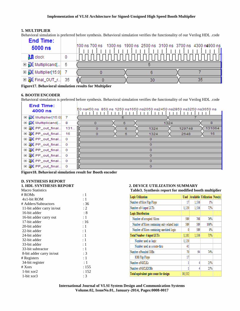
5. MULTIPLIER
Behavioral simulation is preferred before synthesis. Behavioral simulation verifies the functionality of our Verilog HDL .code
Figure17. Behavioral simulation results for Multiplier
6. BOOTH ENCODER
Behavioral simulation is preferred before synthesis. Behavioral simulation verifies the functionality of our Verilog HDL .code
Figure18. Behavioral simulation result for Booth encoder
D. SYNTHESIS REPORT
1. HDL SYNTHESIS REPORT
Macro Statistics
# ROMs : 1
4x1-bit ROM : 1
# Adders/Subtractors : 36
11-bit adder carry in/out : 2
16-bit adder : 8
16-bit adder carry out : 1
17-bit adder : 16
20-bit adder : 1
22-bit adder : 1
24-bit adder : 1
32-bit adder : 1
33-bit adder : 1
33-bit subtractor : 1
8-bit adder carry in/out : 3
# Registers : 1
34-bit register : 1
# Xors : 155
1-bit xor2 : 152
1-bit xor3 : 3
2. DEVICE UTILIZATION SUMMARY
Table3. Synthesis report for modified booth multiplier

P. AVINASH, S.DEEPIKA
International Journal of VLSI System Design and Communication Systems
Volume.02, IssueNo.01, January-2014, Pages:0008-0017
3. TIMING SUMMARY
Speed Grade: -8
Minimum period: No path found
Minimum input arrival time before clock: 40.014ns
Maximum output required time after clock: 5.783ns
Maximum combinational path delay: No path found
Total memory usage is 166340 kilobytes
V. CONCLUSION
This work presents a functional unit which is designed
with multiplier-accumulator (MAC), addition, subtraction
and sum of absolute difference. A Modified Booth
multiplier circuit is used for MAC architecture. Compared
to other circuits, the Booth multiplier has the highest
operational speed and less hardware count. The basic
building blocks for the unit are identified and each of the
blocks is analyzed for its performance.MAC unit is
designed with enable to block. Using this block, the MAC
unit is constructed and calculated for the MAC unit
parameters. The presented technique explores its
applications in multimedia/DSP computations, where the
theoretical analysis and the realization issues are fully
discussed. In this project Xilinx-ISE tool is used for logical
verification, synthesizing performing placing & routing
operation for system verification.
In future it can be extended to floating point numbers
also with the supportive EDA tools. By using transistor
level implementation for the carry save logic the design
reduces the total area required compared to gate level
designs. It will extend to other bands and also there is
chance to improve the speed somewhat more by changing
architecture.
VI. REFERENCES
[1] Soojin Kim and Kyeongsoon Cho “Design of High-
speed Modified Booth Multipliers Operating at GHz
Ranges” World Academy of Science, Engineering and
Technology 61 2010.
[2] Magnus Sjalander and Per Larson-Edefors. “The Case
for HPM-Based Baugh-Wooley Multipliers,” Chalmers
University of Technology,Sweden, March 2008.
[3] Z Haung and M D Ercegovac, “High performance Low
Power left to right array multiplier design” IEEE
rans.Computer, vol 54 no3, page 272-283 Mar 2005.
[4] Aswathy Sudhakar, and D. Gokila, “Run-Time
configurable Pipelined Modified Baugh-Wooley
Multipliers,” Advances in Computational Sciences and
Technology ISSN 0973-6107 Volume 3 Number 2 (2010)
pp. 223–235.
[5] Myoung-Cheol Shin, Se-Hyeon Kang, and In-Cheol
Park, “An Area-Efficient Iterative Modified-Booth
Multiplier Based on Self-Timed Clocking,” Industry, and
Energy through the project System IC 2010, and by IC
Design Education Center (IDEC).
[6] Leandro Z. Pieper, Eduardo A. C. da Costa, Sérgio J.
M. de Almeida, “Efficient Dedicated Multiplication Blocks
for2´s Complement Radix-2m Array Multipliers,”
JOURNAL OF COMPUTERS, VOL. 5, NO.10,
OCTOBER 2010.
[7]Wen-Chang Yeh and Chein-Wei Jen, “High-speed
Booth encoded parallel multiplier design,” IEEE Trans. on
Computers, vol. 49, isseu 7,pp. 692-701, July 2000.
[8] Jung-Yup Kang and Jean-Luc Gaudiot, “A simple high-
speed multiplier design,” IEEE Trans. on Computers, vol.
55, issue 10, Oct. pp.1253-1258, 2006.