implementation of baugh-wooely multiplier and modified...
TRANSCRIPT
International Journal of Science, Engineering and Technology Research (IJSETR), Volume 4, Issue 2, February 2015
293
ISSN: 2278 – 7798 All Rights Reserved © 2015 IJSETR
Abstract— High speed, low power consumption are key
requirement to any VLSI design. The power efficient
multipliers play an important role. This paper presents an
efficient implementation of a high speed, low power multiplier
using shift and adds methods of Baugh Wooely Multiplier. This
study presented the design and implementation of Baugh
wooely multipliers using Cadence (Encounter) RTL Complier.
In this work, Modified Baugh Wooely is having least area,
power and delay. The Modified Baugh wooley architecture is
109X faster than Conventional array multiplier and 102X
faster than conventional Baugh Wooley. The operating
frequency of 5 x 5 Design Modified Baugh Wooley multiplier is
160MHz. The Selection of Multiplier should be done depending
on performance measure and application nature.
Index Terms— Baugh Wooely, Cadence, Low Power
Multiplier, RTL Complier.
I. INTRODUCTION
The increasing prominence of portable system and the need
to limit power consumption in very high density ULSI chips
have led to rapid and innovative developments in low power
design. The need for low power design is becoming a major
issue in high performance digital systems, such as micro-
processor, digital signal processing and other applications.
As demands for portable computing and communication are
growing, the power efficient multiplier plays an important
role in Very Large Scale Integration (VLSI) system design.
Multiplication is one of the essential operation in many
algorithm used in Digital Signal Processing (DSP). A
primary requirement of high performance digital system is
high speed multiplication. In many cases multiplier may be
present in critical path and speed of processing is ultimately
get reduced by speed of multiplication. The Multiplier
algorithm is also one of the major contributors to the total
power dissipation. Reducing the power dissipation is key
criteria in design of multiplier. Power consumed by
multipliers can be lowered at various levels of the design
from algorithm to architectures to circuit [15]. The core of
Pramod S. Aswale, Department of E & TC, SITRC, Nashik.
Savitribai Phule Pune University,( Nashik, Maharashtra, India).
Mukesh P. Mahajan , Department of E & TC, SITRC, Nashik.
Savitribai Phule Pune University,( Nashik, Maharashtra, India).
Manjul V. Nikumbh, Department of E & TC, SITRC, Nashik.
Savitribai Phule Pune University,( Nashik, Maharashtra, India).
Omkar S. Vaidya, Department of E & TC, SITRC, Nashik.
Savitribai Phule Pune University,( Nashik, Maharashtra, India).
any processor is the arithmetic and logic unit (ALU). The
ALU combines the addition and subtraction with other
operation. The addition and subtraction of two numbers are
the basic operation in all digital computers. These operations
occur at the machine instruction level and are implemented
using the basic logic gates in arithmetic and logic unit
(ALU) subsystem of the microprocessor. The time needed to
perform these operations affects the performance of
processors. Multiplication is one of the important operations
which requires more complex circuitry than
addition/subtraction operations. Multiplications are
expensive and slow operations. In many computational
problems the performance is dominated by the speed at
which a multiplication operation can be executed.
Multipliers are complex adder arrays. Multiplication consists
of three basic operations: the generation of partial product,
reduction of partial products, final carry propagate
summation [21]. Considering the timing constraints,
dedicated multipliers hardware implementations such as
array multiplier were introduced. Variable size partial
product arrays are not practical for multiplier design and
since a more sophisticated methods were proposed. The
modified booth recoding scheme is one of the more popular
implementation. The advantage of modified booth recoding
algorithm is that, it reduces the number of generated partial
products by half. Bit pair recoding of the multiplier derived
from booth algorithm, reduces the number of summands by a
factor 2. These summands can then be reduced to only two
by using a relatively small number of carry save addition
steps. The final product can be generated by an addition
operation that uses a carry look ahead adder [19]. The partial
sum adders can be rearranged in a tree like fashion, reducing
both the critical path and the number of adder cells required
e.g wallace tree multiplier, Dadda. Due to irregular structure,
it is difficult to place and route during the layout of a
multiplier. A decreased size of the reduction circuit eases the
implementation and improves the performance of the
multiplier [12].
There are a number of techniques that can be used to
perform multiplication. The choice is based upon factors
such as latency, throughput, area and design complexity.
More efficient parallel approach uses some sort of array or
tree of full adders to sum the partial products. The number
of partial products to sum can be reduced using Booth
Encoding and the number of logic levels required to perform
the summation can be reduced with Wallace trees. Wallace
trees are complex to layout and have long irregular wires, so
hybrid structures may be more attractive. Multiplications are
expensive and slow operation. Basically multiplication
process may be viewed to consist of following two steps (1)
Evaluation of partial product (2) Accumulation of the shifted
partial product. Therefore, faster way to implement
Implementation of Baugh-Wooely Multiplier
and Modified Baugh Wooely Multiplier Using
Cadence (Encounter) RTL
Pramod S. Aswale, Mukesh P. Mahajan, Manjul V. Nikumbh, Omkar S. Vaidya
International Journal of Science, Engineering and Technology Research (IJSETR), Volume 4, Issue 2, February 2015
294
ISSN: 2278 – 7798 All Rights Reserved © 2015 IJSETR
multiplication is to resort to an approach similar to manually
computing a multiplication. All the partial products are
generated at same time and organized in an array. A less
number of partial products also reduces the complexity and
as a result increases the speed to accumulate the partial
products. Both solutions can be applied simultaneous.
In [1], full custom flow of Wallace-Tree, Array and Baugh
Wooley multiplier is implemented using low power design
techniques. In design the parallel multipliers,the number of
partial products to be added is the key parameter which
determines the performance of multiplier.
In [2] comparative study of Modified Booth Multiplication
and Baugh Wooley Multiplier is carried out. The 32 bit
multiplier using 65nm and 130nm is designed and simulated
using Cadence software. According to [11] for a 32 bit
multiplier, a Modified Booth implementation has larger
power dissipation, area and only small improvement in delay
compared to Baugh Wooely multiplier implementation.
The [3] presents an efficient high speed multiplier Baugh
Wooely multiplier. In [3], the study of 4 bit pipelined
multiplier is presented and implemented in VHDL. The
parallel multiplier uses less number of adders, as result of
less space is occupied compared to serial multiplier. The
main criteria in the chip fabrication and high performance
system requires that component should be as small as
possible. Baugh wooley two’s compliment signed multipliers
is the best known algorithm for signed multiplication
because it maximizes the regularity of the multiplier and
allow all the partial products to have positive sign bits.
Baugh Wooely technique was developed to design direct
multiplies for twos compliment numbers. A Baugh Wooely
multiplier was used for twos compliment multiplication due
to its efficiency in handling signed bits. The principle
advantage is that sign of all the partial products bits are
positive allowing the product to be formed using array
addition techniques. In conventional twos complement
multiplication there are partial product bits with negative as
well as positive signs.
The [4] presents the implementation of power efficient
BaughWooely multiplier using FPGA Spartan 3 device. The
speed, power and area have a significant impact as per the
specific applications and efficient realization of the
multiplication is important. The Spartan 3 AN FPGA device
could be used to build basic block reasonably. Many DSP
algorithm demands using application specific integrated
circuits. The computation time can be speedup by assigning
computation intensive tasks to hardware and by exploiting
the parallelism in algorithms.
In [5], 16 X 16 bit multiplier is design and implemented.
When the numbers are in the 2’s complement form, the
design of iterative arrays becomes difficult since the sign bit
is embedded in the number itself. The two scheme which
reduces these problems are the Pezaris and Baugh Wooely
algorithm.The Pezaris, uses different types of cells while
Baugh Wooely algorithm requires true and complemented
form of both numbers.
The power consumed by multipliers can be reduced at
various levels of the design from algorithms to architectures
to circuit and device level. Reference [8]- [12] provides a
good inside into the problem and design optimizations at all
the hierarchy levels.
II. BAUGH WOOELY TWO’S COMPLEMENT SIGNED MULTIPLIER
When the operands are in two’s complement form, the
design of iterative arrays becomes more difficult since the
sign bit is embedded in the number itself. Direct two’s
complement multiplication arrays have been proposed where
the cells used are either more complex or the number of cells
is significantly larger than for the positive-number multiplier
array [16]. Baugh and Wooley modified the multiplication
matrix into a form that contains only positively weighted
partial products. To accomplish this, both the true and
complement values of the operands are needed. There is also
a slight increase in the number of adding cells and in the
multiplication time. The resulting array, however, uses only
Type 0 full adder cells. This uniformity is particularly
advantageous for LSI implementation. Multiplying two 2’s
complement numbers. Let us consider two n-bit numbers A
and B can be represented as
)1.......(....................222
0
1
1
in
i
i
n
n aaA
)2.......(....................222
0
1
1
in
i
i
n
n bbB
Where the sai
'
and sbi
'
are the bits in A and B respectively
and 1na and 1nb are sign bits. The product P=A x B is then
given by the following equation.
)3.........(..........2222
22
22(*)22(*
2
0
1
12
0
1
1
2
0
2
0
22
11
2
0
1
1
2
0
1
1
n
j
j
jn
nn
i
i
ni
n
n
i
n
j
ji
ji
n
nn
n
j
ji
j
n
n
n
i
i
i
n
n
baba
baba
bbaaBAP
Above equation indicates that the find product is obtained by
subtracting the last two positive terms from the first two
terms. One important complication in the development of the
efficient multiplier implementation is the multiplication of
two’s compliment signed numbers.
Baugh Wooley two’s compliment signed multipliers is the
best known algorithm for signed multiplication because it
maximizes the regularity of the multiplier and allow all the
partial products to have positive sign bits Baugh and Wooley
have proposed an algorithm for direct two’s complement
array multiplication. The principal advantage of their
algorithm is that the signs of all summands are positive, thus
allowing the array to be constructed entirely with
conventional type 0 full adders, whereas Pazaris two’s
complement multiplier uses mixture types of full adders.
The Baugh Wooley algorithm is a relatively straightforward
way of doing signed multiplications when multiplying two’s
complement number directly each of the partial products to
be added is a signed numbers. Thus each partial product has
to be sign extended to the width of the final product in order
to form a correct sum by Carry Save Adder(CSA) tree.
According to Baugh Wooley approach, an efficient method
of adding extra entries to the bit matrix is suggested to avoid
having to deal with the negatively weighted bits in partial
product matrix. In equation (write equation no here), rather
than doing a subtraction operation, we can obtain the 2’s
complement of the last two term and add all terms to get the
International Journal of Science, Engineering and Technology Research (IJSETR), Volume 4, Issue 2, February 2015
295
ISSN: 2278 – 7798 All Rights Reserved © 2015 IJSETR
final product. The last two terms are n-1 bits each that
extend in binary weight from position 2n−1
up to 22n−3
. On the
other hand, the final product is 2n bits and extends in binary
weight from 20 upto 2
2n−1. We pad each of the last two terms
in equation 4 with zero’s to obtain a 2n-bit number to be
able to add them to the other terms. The padded terms
extend in binary weight from 20 upto 2
2n−1. The 2n-bit full
precision product PFP can be written as
)4.......(..........))........122(2
)122(2
22(*
2
0
1
11
2
0
1
11
2
0
2
0
22
11
n
i
i
jn
nn
n
j
j
jn
nn
n
i
n
j
ji
ji
n
nnFP
xy
yx
yxyxYXP
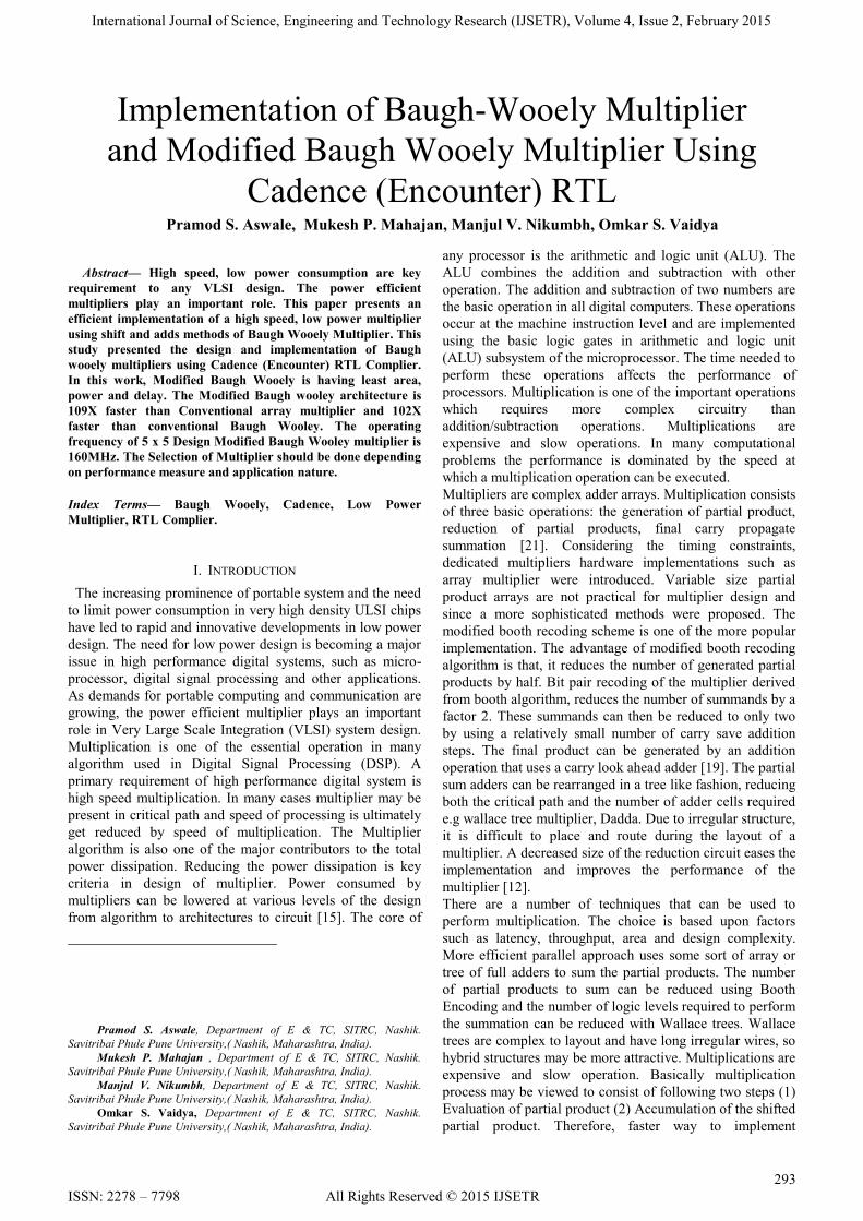
Equation 4 shows the Baugh Wooley algorithm [13].The
schematic circuit diagram of a 5-by-5 Baugh-Wooley array
multiplier is shown in Figure 1.
Figure 1: Schematic Circuit Diagram of a 5-by-5 Baugh-
Wooley Array Multiplier
Example of Baugh-Wooley Algorithm
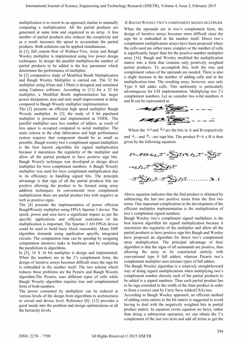
III. MODIFIED BAUGH WOOLEY MULTIPLIER
Conventional Baugh Wooley Multiplier method increases
the height of the longest column by two, which may lead to a
greater delay through the carry save adder tree. As shown in
Tabular bit form 4.3, column height is 7, requiring an extra
carry save adder level. Removing b4from the fourth column
and writing into b4entries in the third column, which has
only four entries, can reduce the extra delay. Thus, the
maximum number of entries in one column becomes six. All
negatively weighted a4b4terms can be transferred to the
bottom row, which leads to two negative numbers in the last
two rows, where a subtraction operation from the sum of all
the positive elements is necessary. Instead of subtracting
a4b4 two’s complement of a can be added b4times. This
method is known as the Modified Baugh Wooely Algorithm.
Fig. 2 shows the schematic diagram of Modified Baugh
Wooely algorithm for 5 X 5 bit multiplier.
Figure 2: The Schematic Circuit Diagram of a 5-by-5
Modified Baugh-Wooley array multiplier.
IV. SIMULATION RESULTS AND DISCUSSION
The code for multiplier is written in Verilog language. The
RTL Compiler is used to compile the code. The Encounter
(cadence) software is used for floor planning, power
International Journal of Science, Engineering and Technology Research (IJSETR), Volume 4, Issue 2, February 2015
296
ISSN: 2278 – 7798 All Rights Reserved © 2015 IJSETR
planning and routing purpose [22]. The functionality of the
schematic is verified using Virtuoso (cadence) software. The
major part of the design entry was done at the transistor
schematic level. The layout where done in an attempt at
estimating the area of the multiplier. Designs were entered
using Cadence RTL compiler, using Encounter floor-
planning, power-planning and routing is carried out.
Cadence Virtuoso for pre layout and post layout simulation
is using targeting NCSU AMI06 CMOS technology.
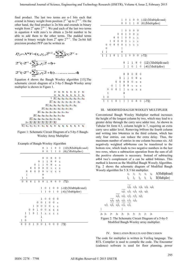
Figure 3: Test Bench Circuit for Simulation
Figure 4: Functionality Proof: Two’s Complement Array
Multiplier Input Wave form
Figure 5: Functionality Proof: Two’s Complement Array
Multiplier Output Wave form
Figure 4 and Figure 5 show the input and output waveform
of array multiplier. To verify the functionality of multiplier,
the Analog Design Environment (ADL) is used.
When two numbers are negative, it will be in two’s
complement form. The two’s complement of each is taken to
convert it to a positive number, and then the two numbers
are multiplied. The product is kept as a positive number and
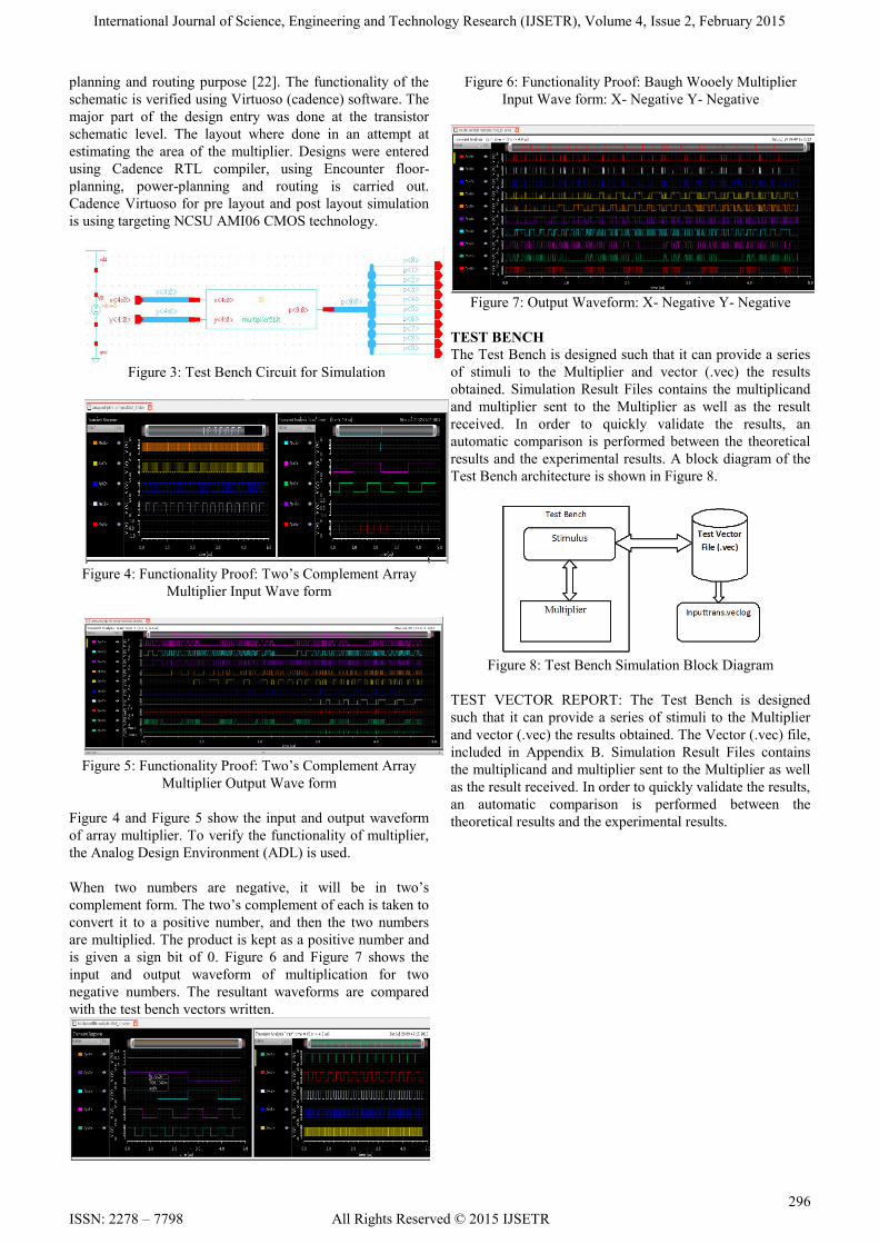
is given a sign bit of 0. Figure 6 and Figure 7 shows the
input and output waveform of multiplication for two
negative numbers. The resultant waveforms are compared
with the test bench vectors written.
Figure 6: Functionality Proof: Baugh Wooely Multiplier
Input Wave form: X- Negative Y- Negative
Figure 7: Output Waveform: X- Negative Y- Negative
TEST BENCH
The Test Bench is designed such that it can provide a series
of stimuli to the Multiplier and vector (.vec) the results
obtained. Simulation Result Files contains the multiplicand
and multiplier sent to the Multiplier as well as the result
received. In order to quickly validate the results, an
automatic comparison is performed between the theoretical
results and the experimental results. A block diagram of the
Test Bench architecture is shown in Figure 8.
Figure 8: Test Bench Simulation Block Diagram
TEST VECTOR REPORT: The Test Bench is designed
such that it can provide a series of stimuli to the Multiplier
and vector (.vec) the results obtained. The Vector (.vec) file,
included in Appendix B. Simulation Result Files contains
the multiplicand and multiplier sent to the Multiplier as well
as the result received. In order to quickly validate the results,
an automatic comparison is performed between the
theoretical results and the experimental results.

International Journal of Science, Engineering and Technology Research (IJSETR), Volume 4, Issue 2, February 2015
297
ISSN: 2278 – 7798 All Rights Reserved © 2015 IJSETR
Figure 9: Test vector report : Both Numbers are Negative
Delay Analysis (worst path)
Register transfer level (RTL) Timing Analysis (RTA) can
provide accurate timing analysis of designs as early as
possible in the design cycle. Performing timing analysis at
the Register transfer level (RTL) level is faster and much
more cost effective than waiting to find the same problems
during timing analysis at the gate-level or layout-level.
Figure 10 shows the worst case path for Modified Baugh
Wooley Multiplier. If Slack time is positive, the tool is
indicating that the signal arrives at the register on the right
much earlier than is needed. This means that the circuit can
work with a much higher clock frequency. As shown in
figure 10, the path from input bit x[1] to output bit p[8] is
having more delay compare to other. The total delay of
worst case path is 6.219ns. The maximum clock frequency
of the multiplier is 160MHz. If slack time becomes negative,
then circuit does not meet timing. One has to find the
maximum clock frequency upto which slack time is positive
i.e. near to one. Table 5.6 shows the performance measures
for various multiplier architectures. It is observed that the
Modified Baugh Wooley multiplier is 1.5 times faster than
Conventional Baugh Wooley multipler.
Figure 10: Timing Report: Worst Path Delay
Table 1: Comparison of various Multipliers Multiplier Type Power Dissipation
(mW)
Area
(
m2)
Delay
(ns)
Array Multiplier
(Conventional)
8.909 83160 8.693
Baugh Wooely
Multiplier
10.88 87912 9.62
Modified Baugh
Wooely Multiplier
10.17 62646 6.219
Post Layout Simulation
The electrical performance of a full-custom design can be
best analyzed by performing a post-layout simulation on the
extracted circuit net-list. The detailed (transistor-level)
simulation performed using the extracted netlist will provide
a clear assessment of the circuit speed, the influence of
circuit parasitic such as parasitic capacitances and
resistances. After perform the LVS (Layout vs. Schematic),
RC extraction of the design is carried out to find parasitic
(resistance and capacitance) to carry out post layout
simulations. Figure 11 shows the RC extracted diagram.
Table 2 shows the power consumption of Modified Baugh
Wooley Multiplier for the (Test Vector case: Both Numbers
are positive) pre-layout and post-layout simulation. In
Digital circuit, power consumption is increased in physical
layout design due to parasitic components.
Figure 11: RC Extracted View of 5 Bit Modified Baugh
Wooley Multiplier
Table 2: Comparison of Power Pre and Post Layout
Pre layout (mW) Post Layout
(mW)
Modified Baugh
Wooely
Multiplier
7.36 7.47
International Journal of Science, Engineering and Technology Research (IJSETR), Volume 4, Issue 2, February 2015
298
ISSN: 2278 – 7798 All Rights Reserved © 2015 IJSETR
V. CONCLUSION
An 5-bit signed multiplier was design using cadence
IC615 using NCSU ami06, layout them in Encounter by
cadence and the analysis of average dynamic power
dissipation was done. The Modified Baugh wooley
architecture is 109X faster than Conventional array
multiplier and 102X faster than conventional Baugh
Wooley. Baugh Wooley consumes more power as compared
to conventional Baugh Wooley. Power can be further reduce
by implementing the design using latest technological node
such as 45nm, 65nm etc we can summarized some of the
important design concepts as
1. Select the right structure before starting an elaborate
circuit optimization.
2. Determine the critical timing path through the circuit.
3. Power and speed can be traded off through a choice of
circuit sizing, supply voltage and transistor thresholds.
There is tremendous scope in design of multiplier in
different architectures. The Baugh Wooley is used for 2’s
complement signed multiplication. There are other
architectures for 2’s complement signed multiplications. The
same can be implemented using latest technology node such
as 22nm, 32nm, 45nm which will reduce power and increase
the speed.
REFERENCES
[1] P.V. Rao, C Prasanna Raj, S. Ravi, “VLSI Design and Analysis of
Multipliers for Low Power”, Fifth International Conference on
Intelligent Information Hiding and Multimedia Signal
Processing”,2009.PP-1354-1357.
[2] M. Sjlander and P. Larsson-Edefors, “High-Speed and Low-Power
Multipliers Using the Baugh-Wooley Algorithm and HPM Reduction
Tree”,Department of Computer Science and Engineering, Chalmers
University of Technology, March 2008.
[3] P. Mohanty, R.Ranjan, “An Efficient Baugh-Wooley Architecture &
Unsigned Multiplication”, International Journal of Computer Science
& Engineering Technology (IJCSET),Vol. 3 No. 4 April 2012,pp-94-
99.
[4] M. H. Rais, B. M. Al-Harthi, Saad I. Al-Askar and Fahad K. Al-
Hussein,“Design and Field Programmable Gate Array Implementation
of Basic Building Blocks for Power Efficient Baugh-Wooley
Multipliers”,American J. of Engineering and Applied Sciences 3 (2):
307-311, 2010.
[5] R. Bajaj, S. Chhabra, S. Veeramachaneni and M B Srinivas, “A
Novel, Low-Power Array Multiplier Architecture”,International
Institute of Information Technology-Hyderabad.
[6] R. B and H. M Kittur, “Faster and Energy Efficient Signed
Multipliers”, School of Electronics Engineering, VIT University.
[7] N. Bandeira, K. Vaccaro, And J. A. Howard, “A Two’s Complement
Array Multiplier Using True Values of the Operands”,IEEE
Transactions On Computers, VOL. c-32, NO. 8, August 1983.
[8] J Rabaey, A Chandrakasan, B Nikolic, “Digital Integrated Circuits A
Design Perspec tive, 2nd Ed., New Jersey : Prentice-Hall Inc, c2003.
[9] Neil H. E. Weste, David Harris, Ayan Banerjee, “CMOS VLSI
Design- A Circuit and Systems Perspective”, Pearson, 2006,pp.345-
357.
[10] Carl Hamacher, Zvonko Vranesic, Safwat Zaky,“ Computer
Organization”,Tata McGraw Hill,2011,pp.376-390.
[11] Wayne Wolf, (2002). Modern VLSI Design: System-On-Chip
Design. 3rd Edition, Pren tice Hall, Upper Saddle River, N.J.
[12] Partha Sarathi Mohanty,“Design And Implemnetation Of Faster And
Low Power Multipliers”, Department Of E & TC, NIT,Rourkela,
2009.
[13] Erik Brunvand,”Crafting a Chip A Practical Guide to the UofU VLSI
CAD Flow”,School of Computing,University of Utah,August 24,
2006, PP-292-335.
[14] Cadence Design Systems. [Online]. Available:
http://www.cadence.com
Pramod S. Aswale, born in Maharashtra, India in 1982. He has completed
his Diploma in Computer Technology in 2002 and completed BE in
Electronics in 2009 and ME in VLSI and Embedded system in 2013. He is
currently working as Assistant Professor in Department of E & TC, SITRC,
Nashik. His research interest are VLSI, Embedded System, He has
published two papers in International Journal.
Mukesh P. Mahajan, born in Maharashtra, India in 1986.
He has completed his B.E. (E & TC) in 2008 and ME
(VLSI Tech.) in 2012. He is currently working as
Assistant Professor in Department of E & TC, SITRC,
Nashik. His research interests are VLSI, Embedded
System. He has published two papers in International
Journal.
Mr. Manjul V. Nikumbh, born in Maharashtra, India in 1990. He has
completed his B.E (E & TC) in 2013. Currently Pursuing M.E. VLSI &
EMBEDDED SYSTEMS. His research interests are VLSI, Embedded
System.
Omkar S. Vaidya has completed B.E, ME in 2009 and 2012
respectively. He is currently working as Assistant Professor
in Department of E & TC, SITRC, Nashik and pursing Ph.D
from Savitribai Phule Pune University. His research interests
are VLSI and Image processing.