impact of scaled technology on radiation testing and hardening
TRANSCRIPT
Impact of Scaled Technology on Radiation Testing and Hardening
Kenneth A. [email protected]
Co-Manager, NASA Electronic Parts and Packaging (NEPP) ProgramLewis M. Cohn
[email protected] Threat Reduction Agency (DTRA)
2“Impact of Scaled Technology on Radiation Testing and Hardening” presented by Kenneth A. LaBel, GOMAC 2005, Las Vegas, NV, April 7, 2005
Outline• Emerging Electronics Technologies
– What has changed and is changing in the commercial semiconductor world
• Radiation Effects and Sources• Challenges to Radiation Testing and
Modeling– TID Trends– Fault isolation– Scaled Geometry– Speed
• Summary/Comments
Note: the emphasis of this presentation is digital technologies and SEE.Some discussion of mitigation implications is included.
3“Impact of Scaled Technology on Radiation Testing and Hardening” presented by Kenneth A. LaBel, GOMAC 2005, Las Vegas, NV, April 7, 2005
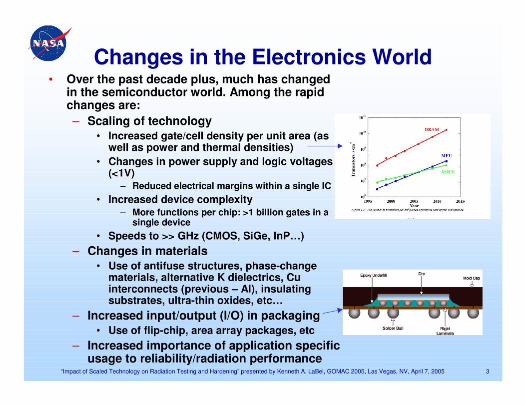
Changes in the Electronics World• Over the past decade plus, much has changed
in the semiconductor world. Among the rapid changes are:– Scaling of technology
• Increased gate/cell density per unit area (as well as power and thermal densities)
• Changes in power supply and logic voltages (<1V)
– Reduced electrical margins within a single IC• Increased device complexity
– More functions per chip: >1 billion gates in a single device
• Speeds to >> GHz (CMOS, SiGe, InP…)– Changes in materials
• Use of antifuse structures, phase-change materials, alternative K dielectrics, Cu interconnects (previous – Al), insulating substrates, ultra-thin oxides, etc…
– Increased input/output (I/O) in packaging• Use of flip-chip, area array packages, etc
– Increased importance of application specific usage to reliability/radiation performance

4“Impact of Scaled Technology on Radiation Testing and Hardening” presented by Kenneth A. LaBel, GOMAC 2005, Las Vegas, NV, April 7, 2005
Radiation Effects and Spacecraft• Critical areas for design in
the natural space radiation environment– Long-term effects causing
parametric and /or function failures
• Total ionizing dose (TID)• Displacement damage
– Transient or single particle effects (Single event effects or SEE)
• Soft or hard errors caused by proton (through nuclear interactions) or heavy ion (direct deposition) passing through the semiconductor material and depositing energy
An Active Pixel Sensor (APS) imagerunder irradiation with heavy ions at Texas
A&M University Cyclotron
5“Impact of Scaled Technology on Radiation Testing and Hardening” presented by Kenneth A. LaBel, GOMAC 2005, Las Vegas, NV, April 7, 2005
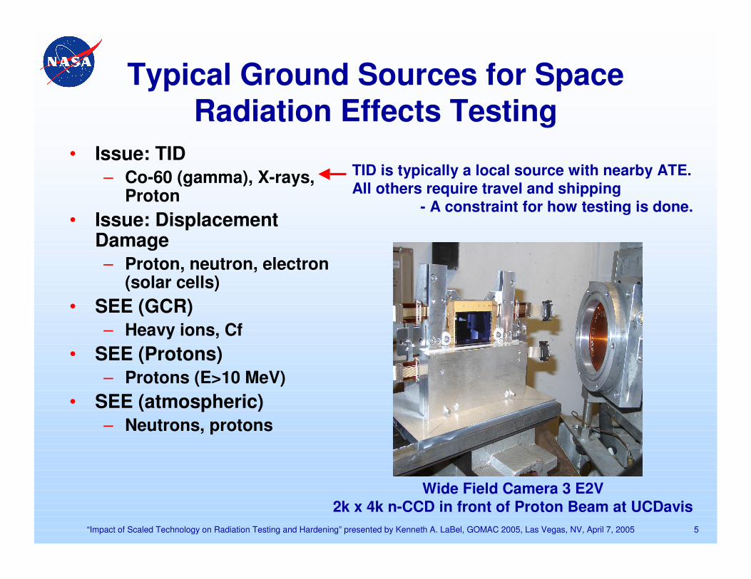
Typical Ground Sources for Space Radiation Effects Testing
• Issue: TID– Co-60 (gamma), X-rays,
Proton• Issue: Displacement
Damage– Proton, neutron, electron
(solar cells)• SEE (GCR)
– Heavy ions, Cf• SEE (Protons)
– Protons (E>10 MeV)• SEE (atmospheric)
– Neutrons, protons
Wide Field Camera 3 E2V2k x 4k n-CCD in front of Proton Beam at UCDavis
TID is typically a local source with nearby ATE.All others require travel and shipping
- A constraint for how testing is done.
6“Impact of Scaled Technology on Radiation Testing and Hardening” presented by Kenneth A. LaBel, GOMAC 2005, Las Vegas, NV, April 7, 2005
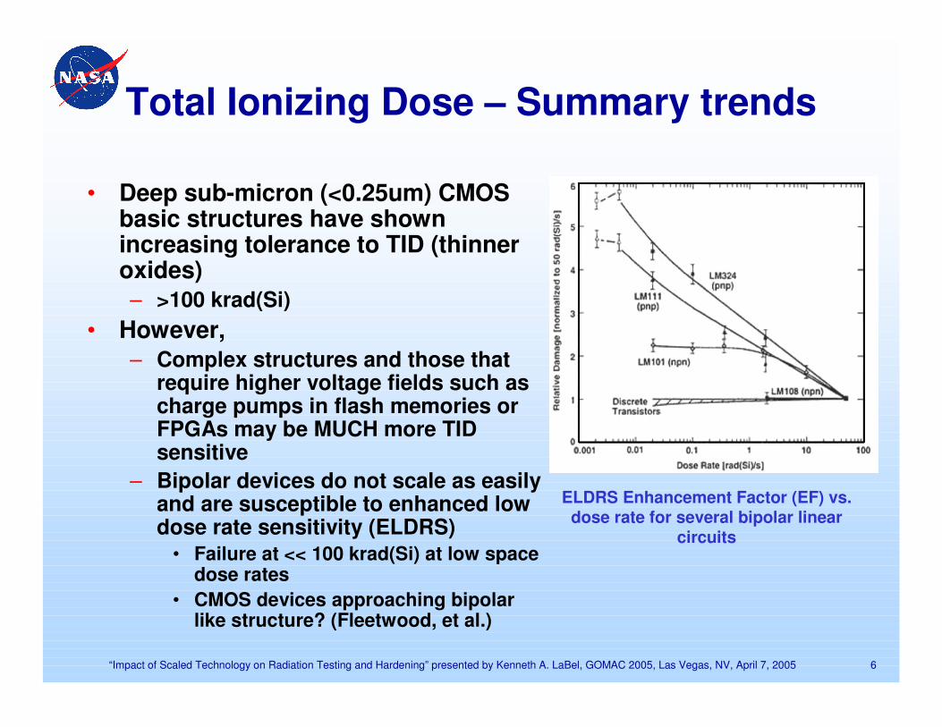
Total Ionizing Dose – Summary trends
• Deep sub-micron (<0.25um) CMOS basic structures have shown increasing tolerance to TID (thinner oxides)– >100 krad(Si)
• However,– Complex structures and those that
require higher voltage fields such as charge pumps in flash memories or FPGAs may be MUCH more TID sensitive
– Bipolar devices do not scale as easily and are susceptible to enhanced low dose rate sensitivity (ELDRS)
• Failure at << 100 krad(Si) at low space dose rates
• CMOS devices approaching bipolar like structure? (Fleetwood, et al.)
ELDRS Enhancement Factor (EF) vs. dose rate for several bipolar linear
circuits
7“Impact of Scaled Technology on Radiation Testing and Hardening” presented by Kenneth A. LaBel, GOMAC 2005, Las Vegas, NV, April 7, 2005
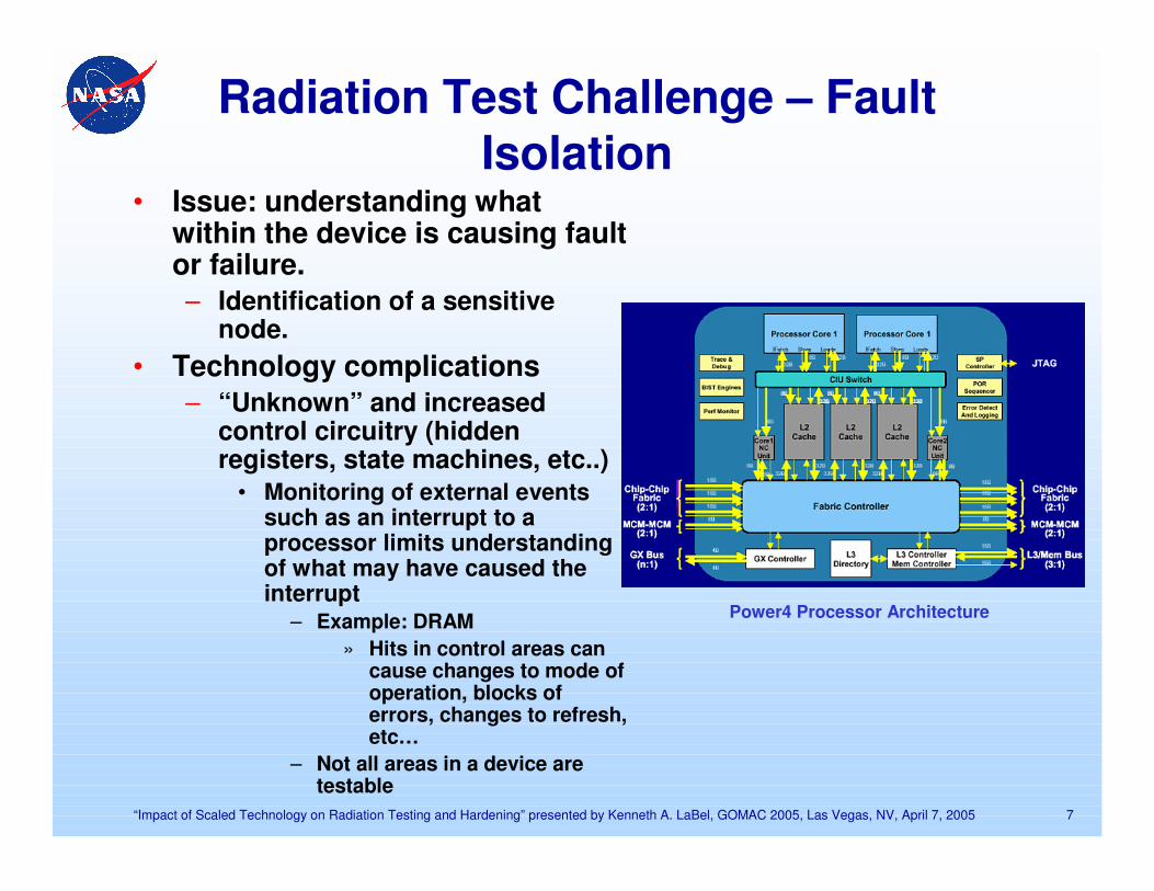
Radiation Test Challenge – Fault Isolation
• Issue: understanding what within the device is causing fault or failure.– Identification of a sensitive
node.• Technology complications
– “Unknown” and increased control circuitry (hidden registers, state machines, etc..)
• Monitoring of external events such as an interrupt to a processor limits understanding of what may have caused the interrupt
– Example: DRAM» Hits in control areas can
cause changes to mode of operation, blocks of errors, changes to refresh, etc…
– Not all areas in a device are testable
Power4 Processor Architecture
8“Impact of Scaled Technology on Radiation Testing and Hardening” presented by Kenneth A. LaBel, GOMAC 2005, Las Vegas, NV, April 7, 2005
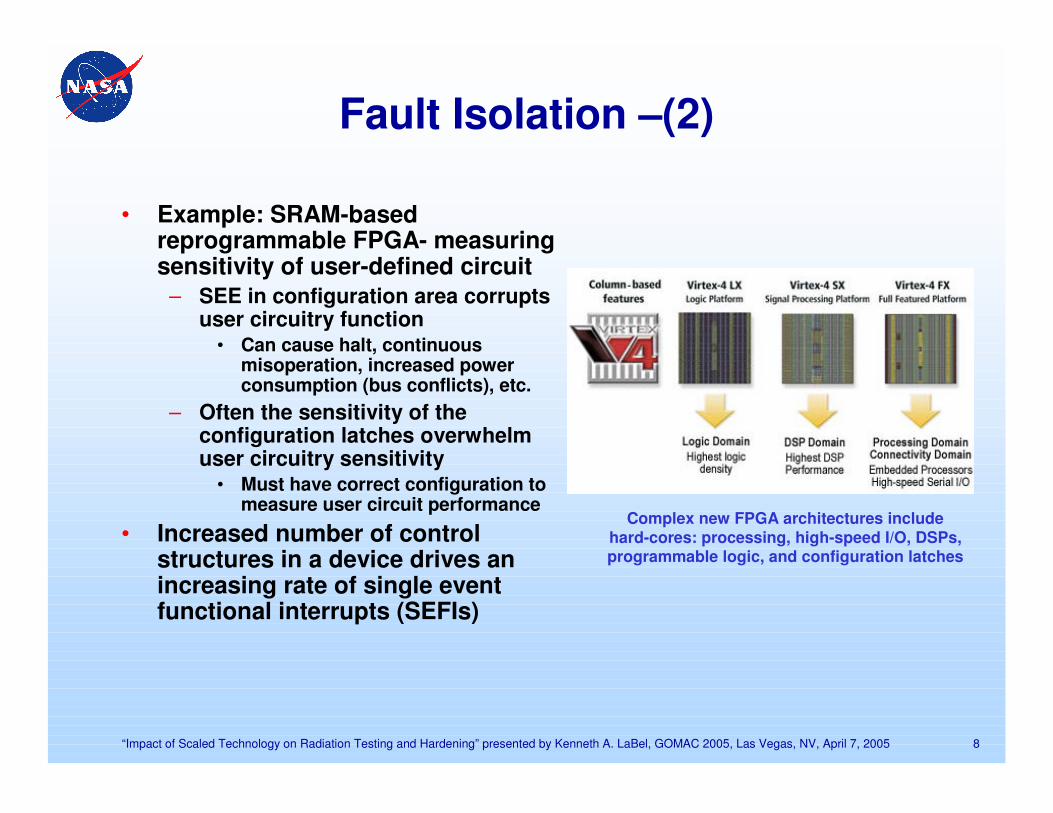
Fault Isolation –(2)
• Example: SRAM-based reprogrammable FPGA- measuring sensitivity of user-defined circuit
– SEE in configuration area corrupts user circuitry function
• Can cause halt, continuous misoperation, increased power consumption (bus conflicts), etc.
– Often the sensitivity of the configuration latches overwhelm user circuitry sensitivity
• Must have correct configuration to measure user circuit performance
• Increased number of control structures in a device drives an increasing rate of single event functional interrupts (SEFIs)
Complex new FPGA architectures includehard-cores: processing, high-speed I/O, DSPs,programmable logic, and configuration latches
9“Impact of Scaled Technology on Radiation Testing and Hardening” presented by Kenneth A. LaBel, GOMAC 2005, Las Vegas, NV, April 7, 2005
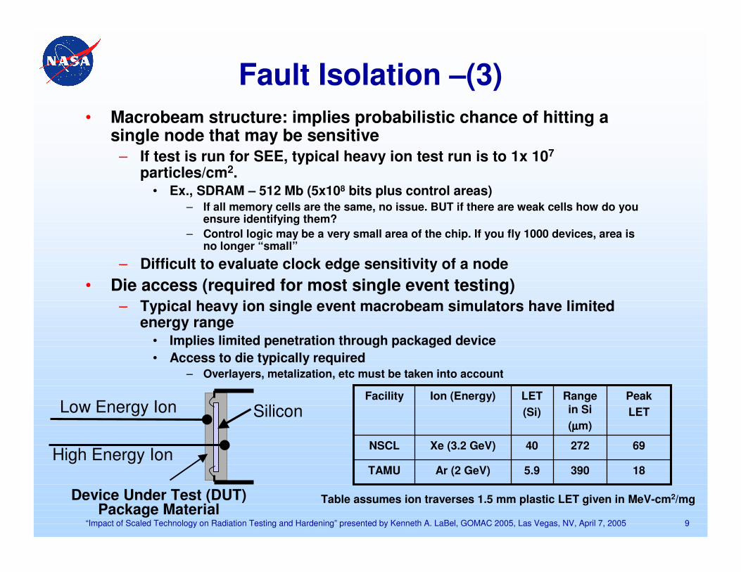
Fault Isolation –(3)• Macrobeam structure: implies probabilistic chance of hitting a
single node that may be sensitive– If test is run for SEE, typical heavy ion test run is to 1x 10⁷
particles/cm2.• Ex., SDRAM – 512 Mb (5x108 bits plus control areas)
– If all memory cells are the same, no issue. BUT if there are weak cells how do you ensure identifying them?
– Control logic may be a very small area of the chip. If you fly 1000 devices, area is no longer “small”
– Difficult to evaluate clock edge sensitivity of a node• Die access (required for most single event testing)
– Typical heavy ion single event macrobeam simulators have limited energy range
• Implies limited penetration through packaged device• Access to die typically required
– Overlayers, metalization, etc must be taken into account
Silicon
Device Under Test (DUT)Package Material
Low Energy Ion
High Energy Ion183905.9Ar (2 GeV)TAMU
6927240Xe (3.2 GeV)NSCL
PeakLET
Range in Si(µµµµm)
LET(Si)
Ion (Energy)Facility
Table assumes ion traverses 1.5 mm plastic LET given in MeV-cm2/mg
10“Impact of Scaled Technology on Radiation Testing and Hardening” presented by Kenneth A. LaBel, GOMAC 2005, Las Vegas, NV, April 7, 2005
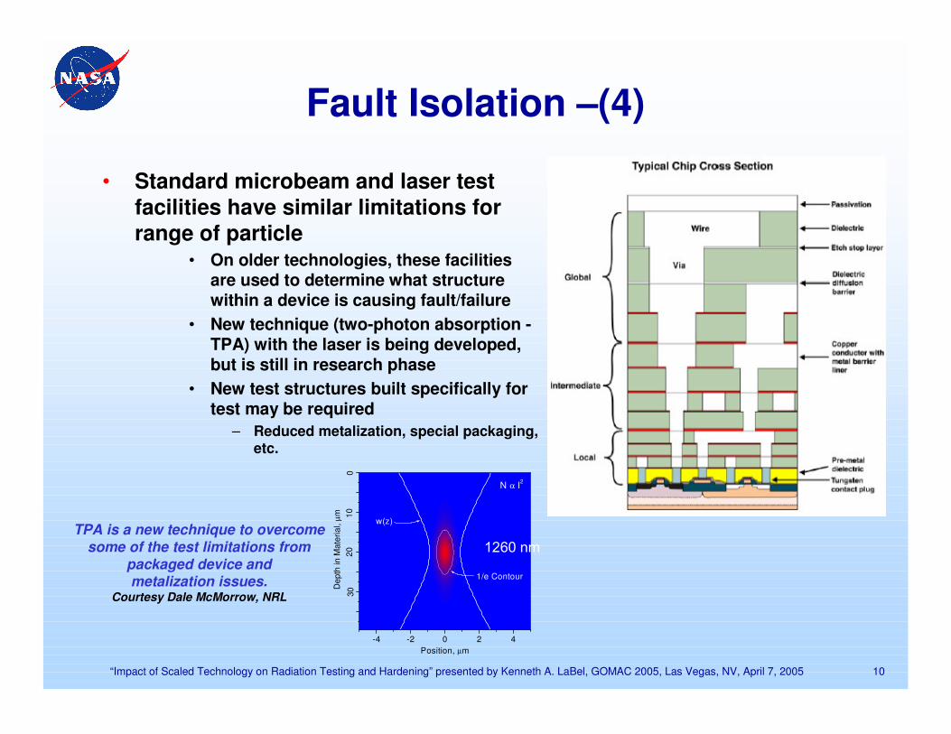
Fault Isolation –(4)
• Standard microbeam and laser test facilities have similar limitations for range of particle
• On older technologies, these facilities are used to determine what structure within a device is causing fault/failure
• New technique (two-photon absorption -TPA) with the laser is being developed, but is still in research phase
• New test structures built specifically for test may be required
– Reduced metalization, special packaging, etc.
-4 -2 0 2 4
030
1020
N α I2
w(z)
1/e Contour
Position, µm
Dep
th in
Mat
eria
l, µm
�������TPA is a new technique to overcome
some of the test limitations frompackaged device andmetalization issues.
Courtesy Dale McMorrow, NRL

11“Impact of Scaled Technology on Radiation Testing and Hardening” presented by Kenneth A. LaBel, GOMAC 2005, Las Vegas, NV, April 7, 2005
Radiation Test Challenge – Geometry
• Issue: the scaling of feature size and closeness of cells• Technology complications
– Multiple node hits with a single heavy ion track• Because of the closeness of transistors and thinness of the
substrate material, a single particle strike can effect multiplenodes potentially defeating hardening schemes.
Litho International Tech RoadmapLithography Technology Requirements – ITRS 2001 Update
2001 2002 2003 2004 2006 2007 2010 2013 2016StartProduction
150nm 130nm 107nm 90nm 70nm 65nm 45nm 32nm 22nmLogic HalfPitch (nm)
90nm 70nm 65nm 53nm 40nm 35nm 25nm 18nm 13nmLogic Gatein Resist (nm)
130nm 115nm 100nm 90nm 70nm 65nm 45nm 32nm 22nmDRAM HalfPitch (nm)
165nm 140nm 130nm 110nm 90nm 80nm 55nm 40nm 30nmContact inResist (nm)
45nm 40nm 35nm 32nm
2005
80nm
45nm
80nm
100nm
28nm 25nm 23nm 18nm 13nm 9nmOverlay
Source: ITRS

12“Impact of Scaled Technology on Radiation Testing and Hardening” presented by Kenneth A. LaBel, GOMAC 2005, Las Vegas, NV, April 7, 2005
Geometry Implications (2)
• Multiple node hits (cont’d)– Ex., memory array
• A single particle strike can spread charge to multiple cells. If the cells are logically as well as physically located
– Standard memory scrub techniques such as Hamming Code can be defeated
• This is not new, simply exacerbated by scaling. Traditional SEU modeling considers particle strikes directly on a transistor
– Charge spreading for strikes near but not on the transistor can generate errors
• Measured error cross-sections may exceed physical cross-sections
– Albeit actual individual targets are smaller for a single particle
• More targets and the spread of non-target hits implied potentially increased error rates per device
– The role of particle directionality and of secondariesrequires future use of physics-based particle interaction codes coupled with circuit tools.
• GEANT4, MCNPX, etc. are the type of codes required– Efforts begun to turn these into tools and not just science
codes
Charge spreading from asingle particle in an
active pixel sensor (APS)array impacts multiple
pixels
13“Impact of Scaled Technology on Radiation Testing and Hardening” presented by Kenneth A. LaBel, GOMAC 2005, Las Vegas, NV, April 7, 2005
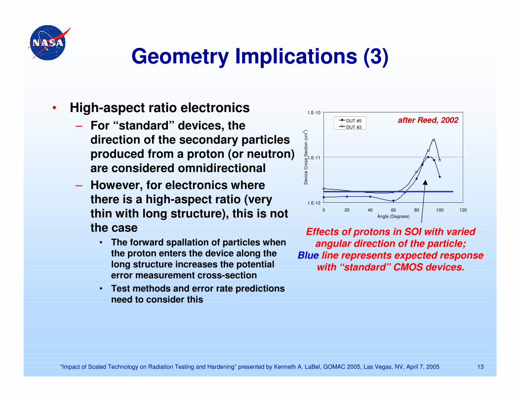
Geometry Implications (3)
• High-aspect ratio electronics– For “standard” devices, the
direction of the secondary particles produced from a proton (or neutron) are considered omnidirectional
– However, for electronics where there is a high-aspect ratio (very thin with long structure), this is not the case
• The forward spallation of particles when the proton enters the device along the long structure increases the potential error measurement cross-section
• Test methods and error rate predictions need to consider this
1.E-12
1.E-11
1.E-10
0 20 40 60 80 100 120Angle (Degrees)
Dev
ice
Cro
ss S
ectio
n (c
m2 )
DUT #5DUT #3
Effects of protons in SOI with varied angular direction of the particle;
Blue line represents expected response with “standard” CMOS devices.
after Reed, 2002
14“Impact of Scaled Technology on Radiation Testing and Hardening” presented by Kenneth A. LaBel, GOMAC 2005, Las Vegas, NV, April 7, 2005
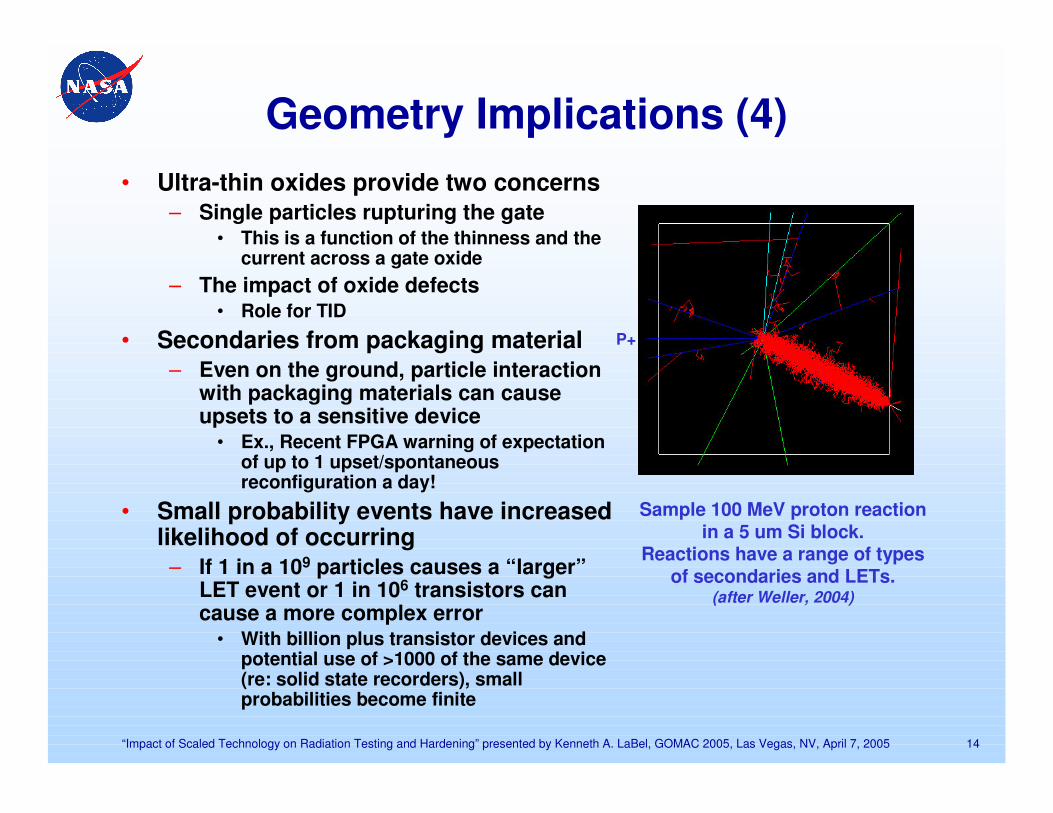
Geometry Implications (4)• Ultra-thin oxides provide two concerns
– Single particles rupturing the gate• This is a function of the thinness and the
current across a gate oxide– The impact of oxide defects
• Role for TID
• Secondaries from packaging material– Even on the ground, particle interaction
with packaging materials can cause upsets to a sensitive device
• Ex., Recent FPGA warning of expectation of up to 1 upset/spontaneous reconfiguration a day!
• Small probability events have increased likelihood of occurring
– If 1 in a 109 particles causes a “larger” LET event or 1 in 106 transistors can cause a more complex error
• With billion plus transistor devices and potential use of >1000 of the same device (re: solid state recorders), small probabilities become finite
Sample 100 MeV proton reactionin a 5 um Si block.
Reactions have a range of typesof secondaries and LETs.
(after Weller, 2004)
P+
15“Impact of Scaled Technology on Radiation Testing and Hardening” presented by Kenneth A. LaBel, GOMAC 2005, Las Vegas, NV, April 7, 2005
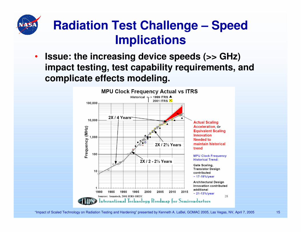
Radiation Test Challenge – Speed Implications
• Issue: the increasing device speeds (>> GHz) impact testing, test capability requirements, and complicate effects modeling.
16“Impact of Scaled Technology on Radiation Testing and Hardening” presented by Kenneth A. LaBel, GOMAC 2005, Las Vegas, NV, April 7, 2005
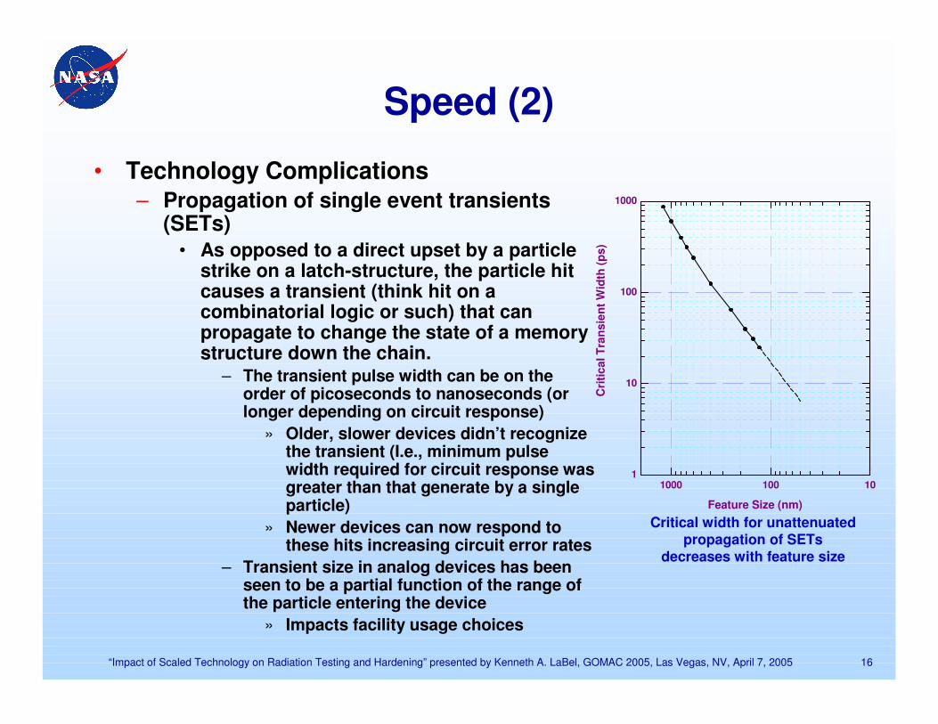
Speed (2)
• Technology Complications– Propagation of single event transients
(SETs)• As opposed to a direct upset by a particle
strike on a latch-structure, the particle hit causes a transient (think hit on a combinatorial logic or such) that can propagate to change the state of a memory structure down the chain.
– The transient pulse width can be on the order of picoseconds to nanoseconds (or longer depending on circuit response)
» Older, slower devices didn’t recognize the transient (I.e., minimum pulse width required for circuit response was greater than that generate by a single particle)
» Newer devices can now respond to these hits increasing circuit error rates
– Transient size in analog devices has been seen to be a partial function of the range of the particle entering the device
» Impacts facility usage choices
1
10
100
1000
Cri
tical
Tra
nsie
nt W
idth
(ps)
10100
Feature Size (nm)
1000
Critical width for unattenuatedpropagation of SETs
decreases with feature size
17“Impact of Scaled Technology on Radiation Testing and Hardening” presented by Kenneth A. LaBel, GOMAC 2005, Las Vegas, NV, April 7, 2005
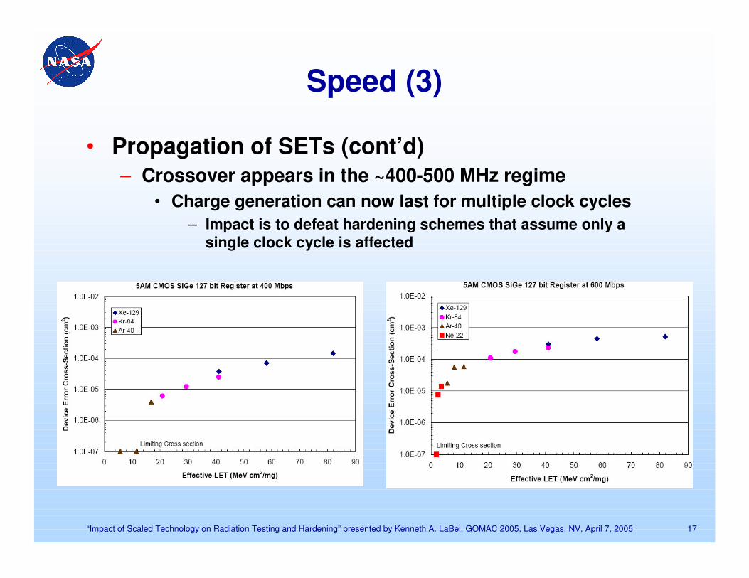
Speed (3)
• Propagation of SETs (cont’d)– Crossover appears in the ~400-500 MHz regime
• Charge generation can now last for multiple clock cycles– Impact is to defeat hardening schemes that assume only a
single clock cycle is affected
18“Impact of Scaled Technology on Radiation Testing and Hardening” presented by Kenneth A. LaBel, GOMAC 2005, Las Vegas, NV, April 7, 2005
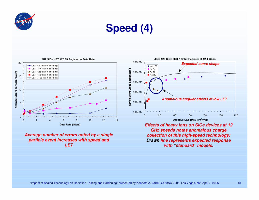
Speed (4)
Jazz 120 SiGe HBT 127 bit Register at 12.4 Gbps
1.0E-07
1.0E-06
1.0E-05
1.0E-04
1.0E-03
1.0E-02
0 20 40 60 80 100 120
Effective LET (MeV cm2/mg)
Dev
ice
Eve
nt C
ross
-Sec
tion
(cm
2 )
Xe-129Kr-84Ar-40Ne-22
Anomalous angular effects at low LET
Effects of heavy ions on SiGe devices at 12 GHz speeds notes anomalous charge
collection of this high-speed technology;Drawn line represents expected response
with “standard” models.
Expected curve shape7HP SiGe HBT 127 Bit Register vs Data Rate
0
5
10
15
20
0 2 4 6 8 10 12 14
Data Rate (Gbps)
Ave
rage
Err
ors
per
Err
or E
vent
LET = 2.75 MeV cm^2/mgLET = 8.57 MeV cm^2/mgLET = 28.8 MeV cm^2/mgLET = 53.0 MeV cm^2/mgLET = 106 MeV cm^2/mg
Average number of errors noted by a single particle event increases with speed and
LET

19“Impact of Scaled Technology on Radiation Testing and Hardening” presented by Kenneth A. LaBel, GOMAC 2005, Las Vegas, NV, April 7, 2005
Speed (5)
Testing at a remote facility requires highly portable test equipment capable of high-speed measurements
– Tester needs to be near the device or utilize high-speed drivers
• Cable runs between the device under test (DUT) and the tester can be up to 75 feet
– Simple devices like a shift register chain can be tested using bit error rate testers (BERTs)
• BERTs can run to ~$1M and tend to be very sensitive to problems from shipping
– At proton test facilities secondaries are generated (neutrons) that can cause failures in the expensive test equipment if they are located near the DUT
– Self-test techniques for testing devices being developed for shift-registers
• Modern reconfigurable FPGA-based test boards being developed to test more generic devices
Beware of stray neutrons impinging on your test
equipment.Here, Borax is shown on top of a power supply to absorb neutrons.
20“Impact of Scaled Technology on Radiation Testing and Hardening” presented by Kenneth A. LaBel, GOMAC 2005, Las Vegas, NV, April 7, 2005
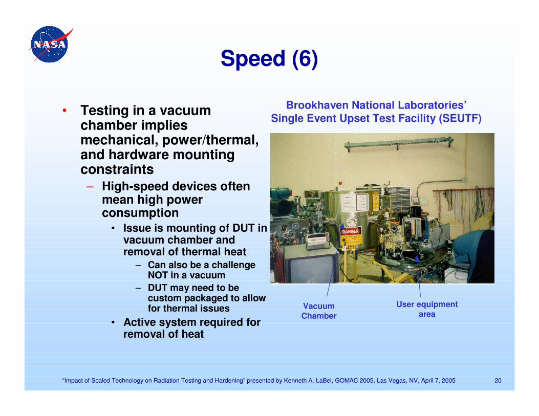
Speed (6)
• Testing in a vacuum chamber implies mechanical, power/thermal, and hardware mounting constraints– High-speed devices often
mean high power consumption
• Issue is mounting of DUT in vacuum chamber and removal of thermal heat
– Can also be a challenge NOT in a vacuum
– DUT may need to be custom packaged to allow for thermal issues
• Active system required for removal of heat
Brookhaven National Laboratories’Single Event Upset Test Facility (SEUTF)
VacuumChamber
User equipmentarea
21“Impact of Scaled Technology on Radiation Testing and Hardening” presented by Kenneth A. LaBel, GOMAC 2005, Las Vegas, NV, April 7, 2005
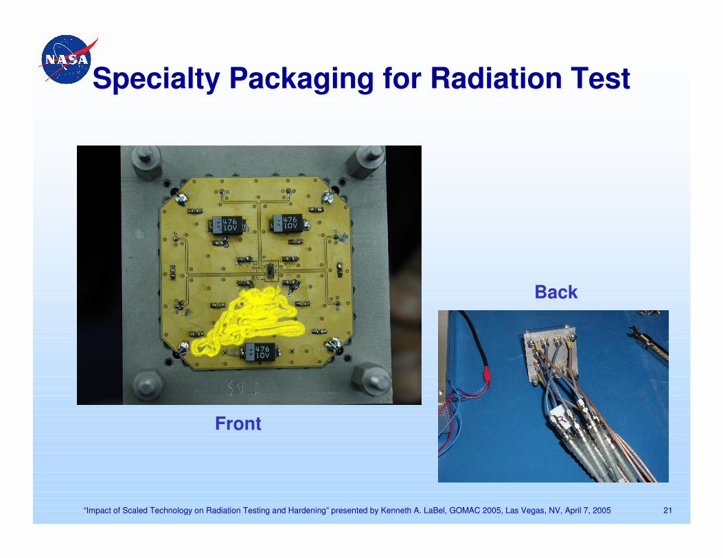
Specialty Packaging for Radiation Test
Front
Back

22“Impact of Scaled Technology on Radiation Testing and Hardening” presented by Kenneth A. LaBel, GOMAC 2005, Las Vegas, NV, April 7, 2005
Summary and Comments
• We have presented a brief overview of SOME of the radiation challenges facing emerging scaled digital technologies
– Implications on using consumer grade electronics
– Implications for next generation hardening schemes
• Comments– Commercial semiconductor
manufacturers are recognizing some of these issues as issues for terrestrial performance
• Looking at means of dealing with soft errors
– The thinned oxide has indicated improved TID tolerance of commercial products
• Hardened by “serendipity”– Does not guarantee hardness or say if the
trend will continue• Reliability implications of thinned oxides
Next Generation SOI:Weak or no body ties will not
solve SEU problems

23“Impact of Scaled Technology on Radiation Testing and Hardening” presented by Kenneth A. LaBel, GOMAC 2005, Las Vegas, NV, April 7, 2005
The Top Five Research/Development Areas Required for Radiation Test and Modeling –
Author’s Opinions
• 5 Understanding extreme value statistics as it applies to radiation particle impacts
• 4 System Risk Tools• 3 High-Energy SEU Microbeam and TPA
Laser• 2 Portable High-Speed Device Testers• 1 Physics Based Modeling Tool
Backup Slides
25“Impact of Scaled Technology on Radiation Testing and Hardening” presented by Kenneth A. LaBel, GOMAC 2005, Las Vegas, NV, April 7, 2005
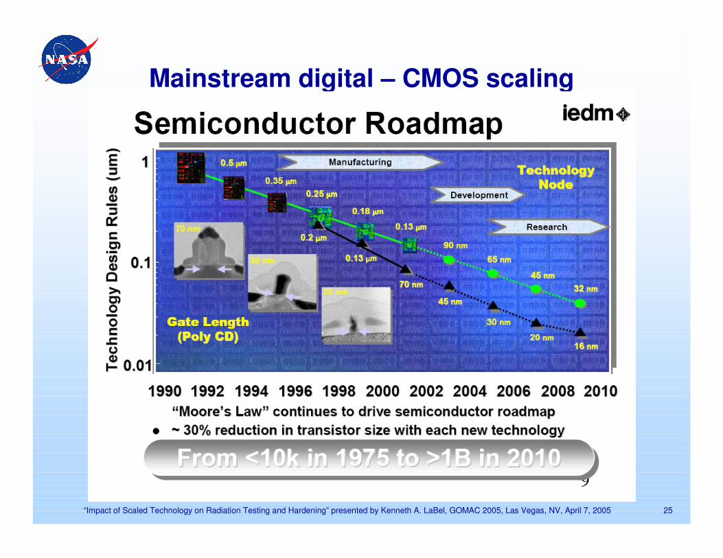
Mainstream digital – CMOS scaling
26“Impact of Scaled Technology on Radiation Testing and Hardening” presented by Kenneth A. LaBel, GOMAC 2005, Las Vegas, NV, April 7, 2005
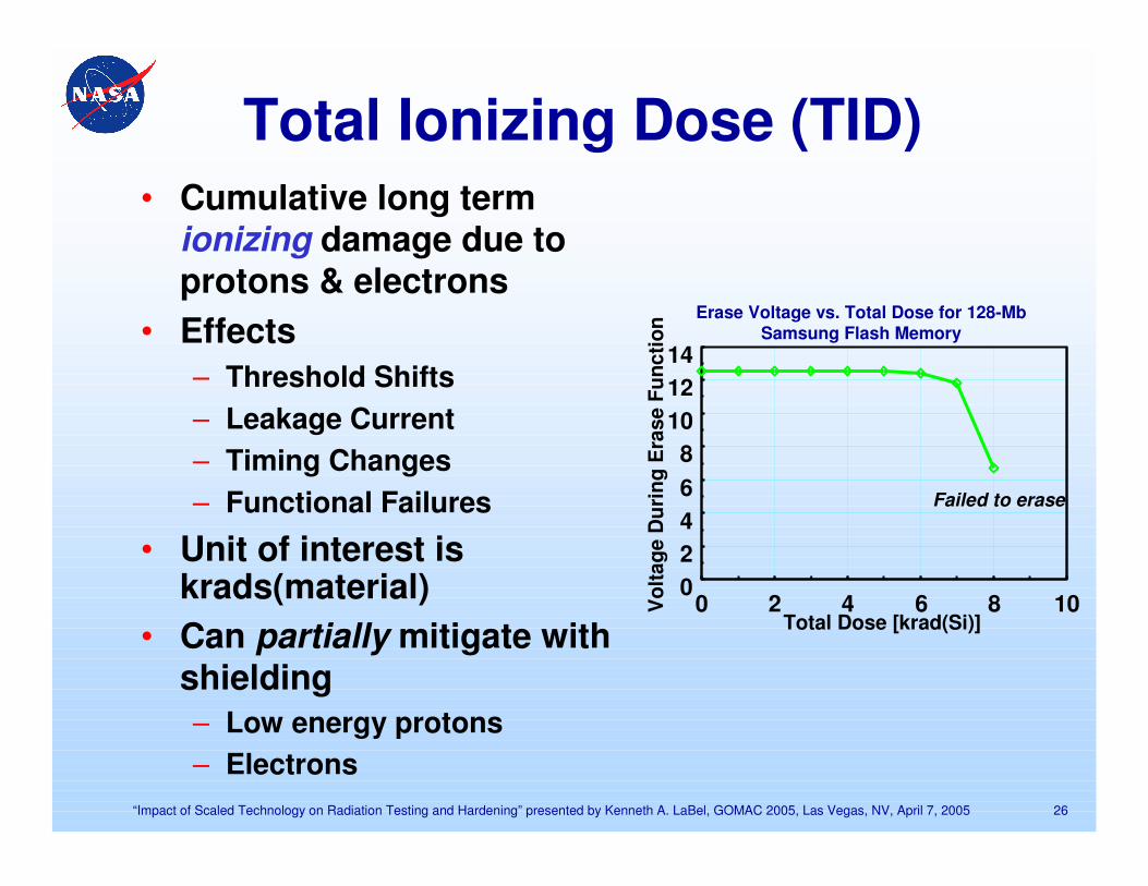
Total Ionizing Dose (TID)• Cumulative long term
ionizing damage due to protons & electrons
• Effects– Threshold Shifts– Leakage Current– Timing Changes– Functional Failures
• Unit of interest is krads(material)
• Can partially mitigate with shielding– Low energy protons– Electrons
Erase Voltage vs. Total Dose for 128-Mb Samsung Flash Memory
02468
101214
0 2 4 6 8 10Total Dose [krad(Si)]
Vol
tage
Dur
ing
Era
se F
unct
ion
Failed to erase

27“Impact of Scaled Technology on Radiation Testing and Hardening” presented by Kenneth A. LaBel, GOMAC 2005, Las Vegas, NV, April 7, 2005
Displacement Damage (DD)• Cumulative long term non-ionizing
damage due to protons, electrons, and neutrons
• Effects– Production of defects which results in
device degradation– May be similar to TID effects– Optocouplers, solar cells, CCDs, linear
bipolar devices
• Unit of interest is particle fluence for each energy mapped to test energy– Non-ionizing energy loss (NIEL) is one
means of discussing• Shielding has some effect - depends on
location of device– Reduce significant electron and some
proton damage
Not par
ticular
ly ap
plicab
le to
CMOS m
icroele
ctro
nics

28“Impact of Scaled Technology on Radiation Testing and Hardening” presented by Kenneth A. LaBel, GOMAC 2005, Las Vegas, NV, April 7, 2005
Single Event Effects (SEEs)• An SEE is caused by a single charged particle as it passes
through a semiconductor material– Heavy ions
• Direct ionization
– Protons for sensitive devices• Nuclear reactions for standard devices• Optical systems, etc are sensitive to direct ionization
• Effects on electronics– If the LET of the particle (or reaction) is greater than the
amount of energy or critical charge required, an effect may be seen
• Soft errors such as upsets (SEUs) or transients (SETs), or• Hard (destructive) errors such as latchup (SEL), burnout (SEB), or
gate rupture (SEGR)
• Severity of effect is dependent on– type of effect– system criticality
Destructive event in a COTS 120V
DC-DC Converter
29“Impact of Scaled Technology on Radiation Testing and Hardening” presented by Kenneth A. LaBel, GOMAC 2005, Las Vegas, NV, April 7, 2005
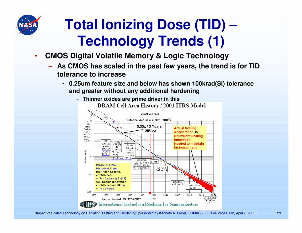
Total Ionizing Dose (TID) –Technology Trends (1)
• CMOS Digital Volatile Memory & Logic Technology– As CMOS has scaled in the past few years, the trend is for TID
tolerance to increase• 0.25um feature size and below has shown 100krad(Si) tolerance
and greater without any additional hardening– Thinner oxides are prime driver in this
30“Impact of Scaled Technology on Radiation Testing and Hardening” presented by Kenneth A. LaBel, GOMAC 2005, Las Vegas, NV, April 7, 2005
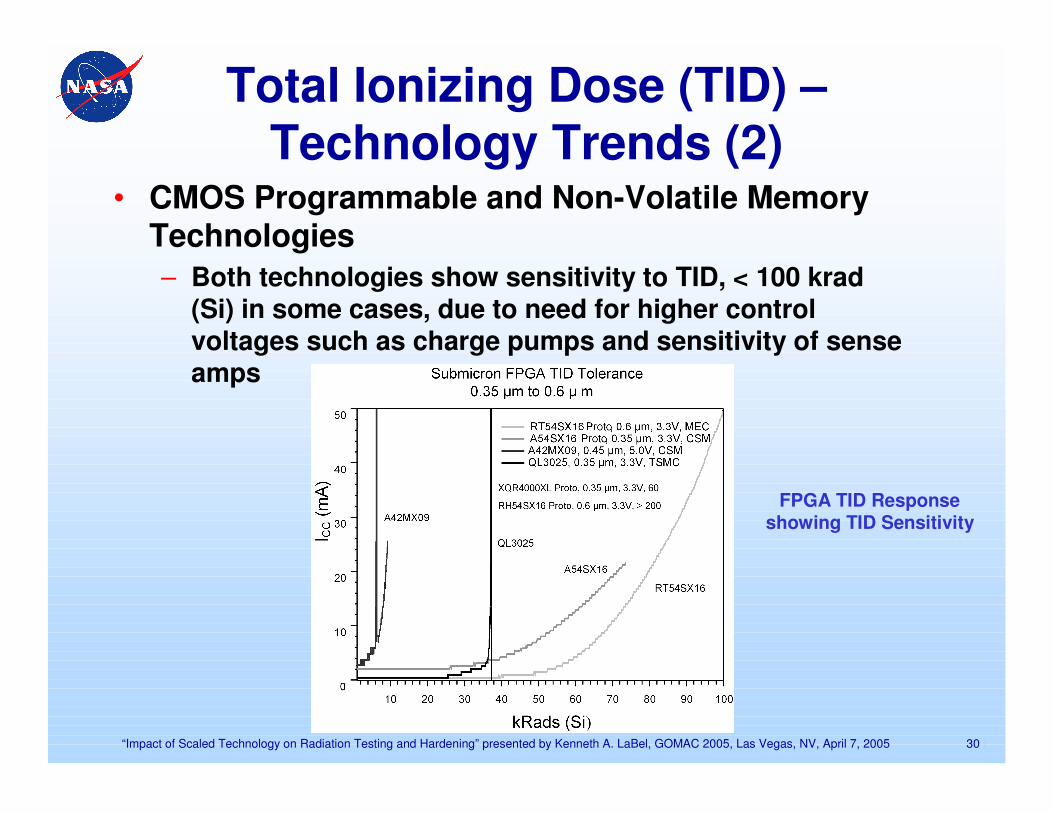
Total Ionizing Dose (TID) –Technology Trends (2)
• CMOS Programmable and Non-Volatile Memory Technologies– Both technologies show sensitivity to TID, < 100 krad
(Si) in some cases, due to need for higher control voltages such as charge pumps and sensitivity of sense amps
FPGA TID Responseshowing TID Sensitivity

31“Impact of Scaled Technology on Radiation Testing and Hardening” presented by Kenneth A. LaBel, GOMAC 2005, Las Vegas, NV, April 7, 2005
Total Ionizing Dose (TID) –Technology Trends (3)
• Bipolar Linear Technologies– Demonstrate extreme
sensitivity to TID, parametric & functional fails < < 100 krads
– Many modern devices subject to Enhanced Low Dose-Rate Sensitivity (ELDRS) Effects
• It has been predicted that this effect may be seen in scaled CMOS as the scaling approaches a bipolar-like structure (Fleetwood, et al.) ELDRS Enhancement Factor (EF) vs.
dose rate for several bipolar linear circuits