impact chang tutorial 2008
TRANSCRIPT

IMPACT • Plasma• 1
IMPACT Seminar
Title: Simulation of Feature Profile Evolution during Plasma-Assisted Processes Faculty: Jane P. Chang Student: John Hoang Department: Chemical and Biomolecular Engineering University: UCLA
IMPACT • Plasma• 2
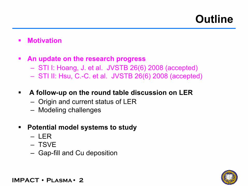
Outline
Motivation
An update on the research progress – STI I: Hoang, J. et al. JVSTB 26(6) 2008 (accepted)– STI II: Hsu, C.-C. et al. JVSTB 26(6) 2008 (accepted)
A follow-up on the round table discussion on LER– Origin and current status of LER – Modeling challenges
Potential model systems to study – LER– TSVE– Gap-fill and Cu deposition

IMPACT • Plasma• 3
Motivation
Stringent control of feature geometry and dimensions futureLower process and development cost by predicting
Henrik Schumacher, CMOS Chip Structure. www.wikimedia.org
Line Edge Roughness (LER)/ Line Width Roughness (LWR)
Chris A. Mack, Field Guide to Optical Lithography, SPIE Field Guide Series, Vol. FG06, Bellingham,
WA, 2006
Back End of Line (BEOL)Atomic Force Microscopy (AFM)
Goldfarb et. al. JVST B 22(2) 2002
Front end of Line (FEOL)
Lam Research. “Etch Technology” www.lamrc.com
Gate Stack Etch
† Adapted from ITRS 2003 Thermal Films Supplemental
Shallow Trench Isolation (STI)
D1
D2
D3
total Si depth
tx1 (nitride)
tx2 (top Si)
tx3 (bot Si)
nitride SWA
top Si SWA
bottom Si side wall angle (SWA)
D4
SixNy
Si
n+
n+
SVG
p+
DVG
p+
STI
p-Si n+ well
STI
STI

IMPACT • Plasma• 4
Shallow Trench Isolation (STI)
† Adapted from ITRS 2003 Thermal Films Supplemental
Critical Parameters (SEM Measurements) D1
D2
D3 total Si depth
tx1 (nitride)
tx2 (top Si)
tx3 (bot Si)
nitride SWA
top Si SWA
bottom Si side wall angle (SWA)
D4
SixNy
Si
CMP planarization
Isolation stack Pattern nitride and strip PR
Trench etch
PRnitrideoxide
Si
Sidewall oxidation and deposit trench oxide
Strip nitride and remove pad oxide
Shallow Trench Isolation Process AMAT DPS IICl2
O2N2
O2N2
Pressure
DC Ratio (Iouter/Iinner)
Ws
Wb
Wafer
pumping ports
Cl2
O2N2
O2N2
Pressure
DC Ratio (Iouter/Iinner)
Ws
Wb
Wafer
pumping ports
STI Etch ParametersP = 25/45 mTWs = 350/500 WWb = 150/250 WDC ratio = 11/30Cl2 = 140/180 sccmN2 = 30/60 sccmO2 = 15/25 sccm
No Oxygen in Feed Gas
SEM Image – Top View

IMPACT • Plasma• 5
Kinetic Model for Si Etch in Cl2 Plasma
0 (1 )( ) ( )
Cl Cl Osg sCl Clζ ζ− −+ ∗ →
( )( ) ( )
cg sCl Clφ+ +∗ →
( )( ) ( ) 4( )4 4c Cls s gSi Cl SiClφ β +
+ → + ∗0
2
2( ) ( ) ( )3 2SiCl
sg s sSiCl Si Cl→+ +∗
0 (1 )( ) ( )
O OClsg sO Oζ ζ− −
+ →∗
( ) ( )SPSiY
s gSi Si→ +∗0
( ) ( )Sis
g sSi Si→+∗
2( ) ( ) ( )Clr
g s gCl Cl Cl→+ +∗
Surface Reaction Surface Reaction (cont)
+
+
Ion incident angle φ (degree from normal)
Poly
Oxide
0
1
2
3
4
0 30 60 900
0.1
0.2Ion Angular Dependence
0
0.4
0.8
1.2
0 10 20 30
Cl/Cl+ = 120 with SiCl2
Cl+ alone with SiCl2
S iC l +
S iC lC l
2+
Flux Ratio
S iC l SiC l C le4 2 2
−
→ +
Etching Yield
0
0.4
0.8
1.2
0 10 20 30
Cl/Cl+ = 120 with SiCl2
Cl+ alone with SiCl2
S iC l +
S iC lC l
2+
Flux Ratio
S iC l SiC l C le4 2 2
−
→ +
Etching Yield
SiCl2 flux
+ArCl
Flux Ratio
Yield
Poly
Oxide
0
1
2
3
4
0 50 100 150 2000.0
0.1
0.2
0.3
0.4Selectivity+
+
0
1
2
3
4
0 100 200 300 400
S iC l +
Etching Yield
75eV Cl+/Cl
55eV Cl+/Cl
35eV Cl+/Cl
ClCl +
Flux Ratio
ClCl +
Flux Ratio
80 eV(Lam TCP)
n/I+ ratio and Eion +
+
Cho, H.S. et al. Mat. Sci. in Semi. Process. 8 (2005) 239Ulal, S.J et al. J. Vac. Sci. Technol. A 20(2) 2002
Rigorous incorporation of physics and chemistry for deposition/etching
IMPACT • Plasma• 6
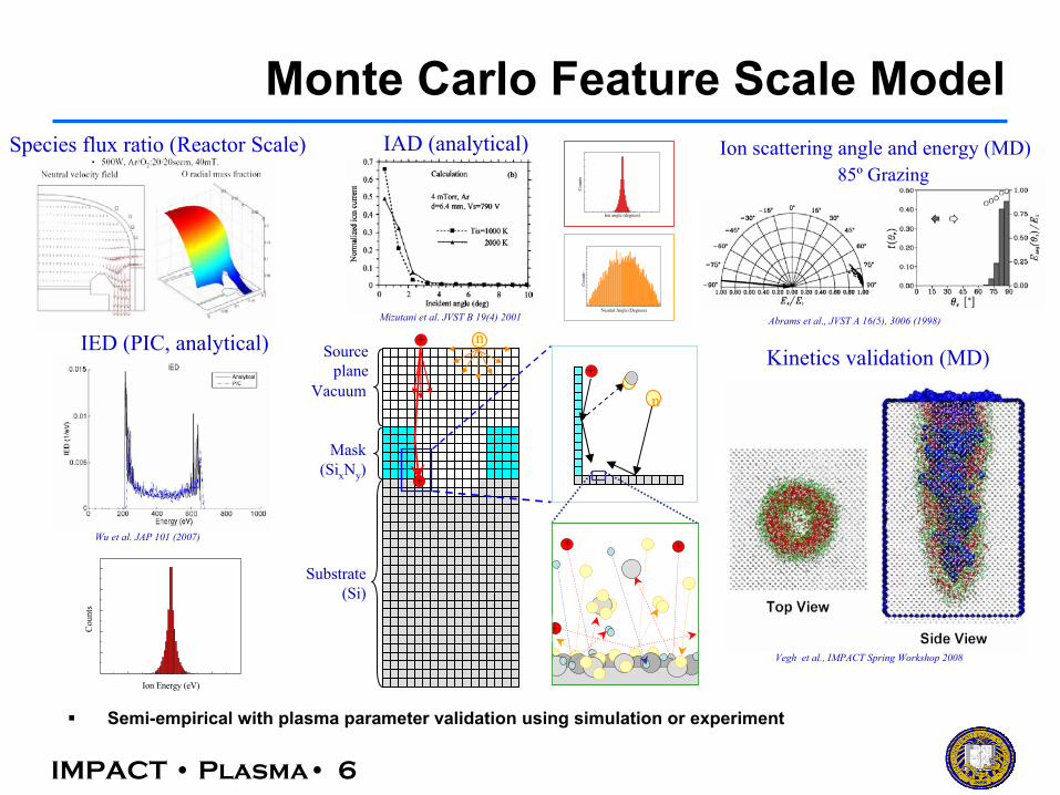
Monte Carlo Feature Scale Model
Vegh et al., IMPACT Spring Workshop 2008
Kinetics validation (MD)
Species flux ratio (Reactor Scale)
Mask (SixNy)
Substrate(Si)
Source plane
Vacuum
+
85º GrazingIon scattering angle and energy (MD)
Abrams et al., JVST A 16(5), 3006 (1998)
IAD (analytical)
Mizutani et al. JVST B 19(4) 2001
Cou
nts
Neutral Angle (Degrees)
Cou
nts
Ion angle (degrees)
Wu et al. JAP 101 (2007)
IED (PIC, analytical)
Cou
nts
Ion Energy (eV)
Semi-empirical with plasma parameter validation using simulation or experiment
+
n
+
+
+
n
+
IMPACT • Plasma• 7
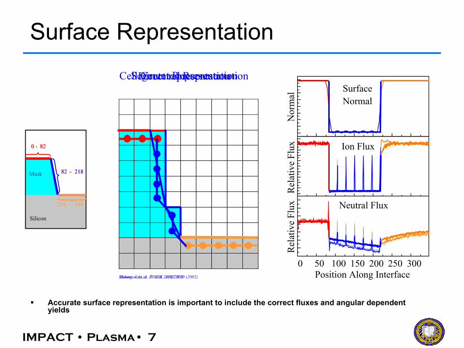
Surface Representation
Accurate surface representation is important to include the correct fluxes and angular dependent yields
0 - 82
82 - 218
218 - 348
0 - 82
82 - 218
218 - 348
Silicon
Mask
Direct representation
0 50 100 150 200 250 300
Ion Flux
Position Along Interface
Rel
ativ
e Fl
uxN
orm
al
Neutral Flux
Rel
ativ
e Fl
ux
SurfaceNormal
Cell Centered RepresentationSegment Representation
Mahorowala, A. P. et al. JVST B 20 (2002)Hoang, J. et al. JVSTB 26(6) 2008
IMPACT • Plasma• 8
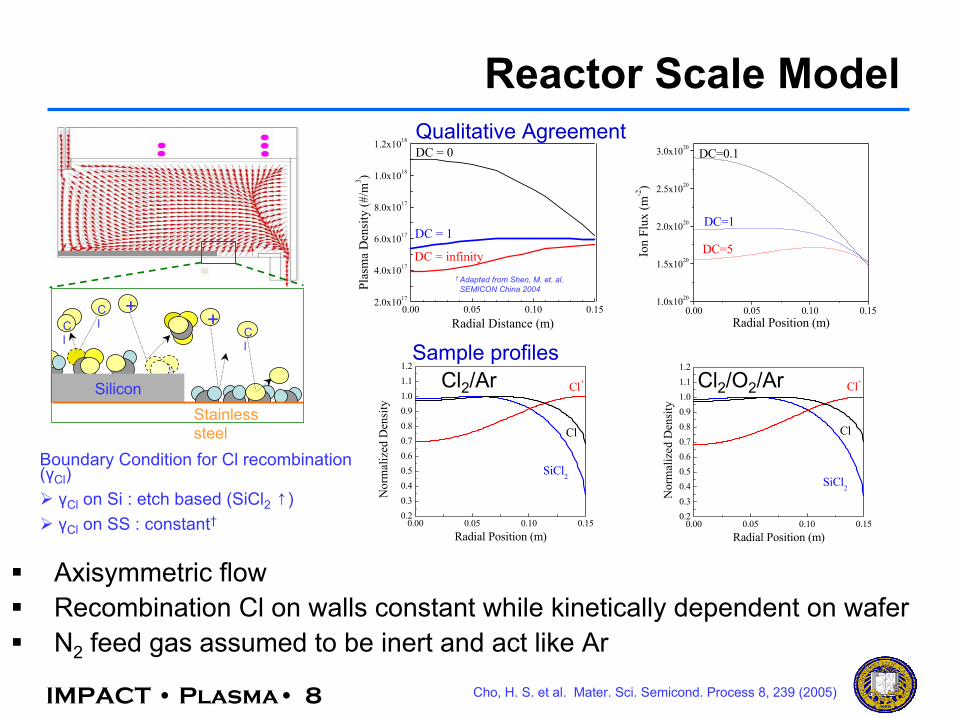
Reactor Scale Model
0.00 0.05 0.10 0.151.0x1020
1.5x10²⁰
2.0x10²⁰
2.5x10²⁰
3.0x10²⁰
DC=5
DC=1
Ion
Flux
(m-2
)
Radial Position (m)
DC=0.1
Axisymmetric flowRecombination Cl on walls constant while kinetically dependent on waferN2 feed gas assumed to be inert and act like Ar
Cho, H. S. et al. Mater. Sci. Semicond. Process 8, 239 (2005)
Boundary Condition for Cl recombination (γCl)γCl on Si : etch based (SiCl2 ↑)γCl on SS : constant†
Silicon
+
Stainless steel
ClC
l Cl
+
Cl2/O2/ArCl2/ArSample profiles
0.00 0.05 0.10 0.150.20.30.40.50.60.70.80.91.01.11.2
Cl
Cl+
Nor
mal
ized
Den
sity
Radial Position (m)
SiCl2
0.00 0.05 0.10 0.150.20.30.40.50.60.70.80.91.01.11.2
Cl
SiCl2
Nor
mal
ized
Den
sity
Radial Position (m)
Cl+
† Adapted from Shen, M. et. al. SEMICON China 2004
Qualitative Agreement
0.00 0.05 0.10 0.152.0x1017
4.0x10¹⁷
6.0x10¹⁷
8.0x10¹⁷
1.0x10¹⁸
1.2x10¹⁸
DC = infinity
DC = 1
DC = 0
Plas
ma
Den
sity
(#/m
3 )
Radial Distance (m)

IMPACT • Plasma• 9
Linking Hybrid Model to SEM
Steady state: link feature scale model to experimentIon flux limited: link feature scale model to reactor scale modelWell planned experiments (one parameter change at a time)
1. Steady state 2. Ion flux limited
Assumptions
Particle count correlated with
measured etched area
0 50 100 150 200 250 300 350 4000123456789
10
235 eV195 eV155 eV
115 eV
75 eV55 eV
Si E
tch
Yie
ld (S
i/Cl+ )
Neutral to Ion Ratio (Cl/Cl+)
35 eV
Allows use of species densities from
qualitatively verified reactor model
Controlled Experiments

IMPACT • Plasma• 10
Hybrid Model Results for STIE
0 1 14 15
0.9
1.0
Nor
mal
ized
Si E
tch
Dep
th
(w.r.
t. ce
nter
)
Radial Position (cm)10 15 20 25 30
-2
0
2
4
6
SWA
Var
iatio
n (%
)
DC Ratio0.0 0.5 14.0 14.5
80
82
84
86
88
Side
wal
l Ang
le (D
eg.)
Radial Position (cm)
0.00 0.05 0.10 0.15 0.20
0.0
0.2
0.4
0.6
0.8
1.0 Cl+
SiCl2
O
Nor
mal
ized
Den
sitie
s
Radial Position (m)
0.00 0.05 0.10 0.150.0
0.1
0.2
0.3
0.4
0.5
0.6
0.7
0.8
Cl S
urfa
ce C
over
age
Radial Position (m)
0.00 0.05 0.10 0.15 0.200
1x10¹⁹
2x10¹⁹
3x10¹⁹
4x10¹⁹
5x10¹⁹
6x10¹⁹
Cl D
ensi
ty (m
-3)
Radial Position (m)
Wafer
Center 10 mm 5 mmEdge
Center 10 mm 5 mmEdge
• Hybrid model captures center-edge variation in etch depth and SWA

IMPACT • Plasma• 11
Hybrid Model Results for STIE
• SWA and depth variation captured using normalized species densities
0.00 0.05 0.10 0.150.0
1.0
2.0
3.0
4.0
5.0
6.0
7.0
SiCl2
Den
sity
x 1
019 (m
-3)
Radial Position (m)
Cl
0.00 0.05 0.10 0.150.0
2.0
4.0
6.0
8.0
Den
sity
x 1
019 (m
-3)
Radial Position (m)
Cl
SiCl2
0.00 0.05 0.10 0.150.0
2.0
4.0
6.0
8.0
Den
sity
x 1
019 (m
-3)
Radial Position (m)
Cl
SiCl2
Center 10 mm 5 mmEdge
0.00 0.05 0.10 0.150.0
1.0
2.0
3.0
4.0
5.0
6.0
7.0
Cl+
Flux
x 1
019 (m
-2s-1
)Radial Position (m)
0.00 0.05 0.10 0.150.0
2.0
4.0
6.0
8.0
Flux
x 1
019 (m
-2s-1
)
Radial Position (m)
Cl+
0.00 0.05 0.10 0.150.0
2.0
4.0
6.0
8.0
Flux
x 1
019 (m
-2s-1
)
Radial Position (m)
Cl+
Ws = 350 W, Wb = 150 W, P = 25 mT, DC = 11, Ar/O2/Cl2 : 30/15/140
Ws = 500 W, Wb = 150 W, P = 25 mT, DC = 30, Ar/O2/Cl2 : 60/15/140
Ws = 500 W, Wb = 150 W, P = 25 mT, DC = 11, Ar/O2/Cl2 : 30/25/180
IMPACT • Plasma• 12
Outline
Motivation
An update on the research progress – STIE Part I: Hoang, J. et al. JVSTB 26(6) 2008 (accepted)– STIE Part II: Hsu, C.-C. et al. JVSTB 26(6) 2008 (accepted)
A follow-up on the round table discussion on LER– Origin and current status of LER – Modeling challenges
Potential model systems to study – LER– TSVE– Gap-fill and Cu deposition

IMPACT • Plasma• 13
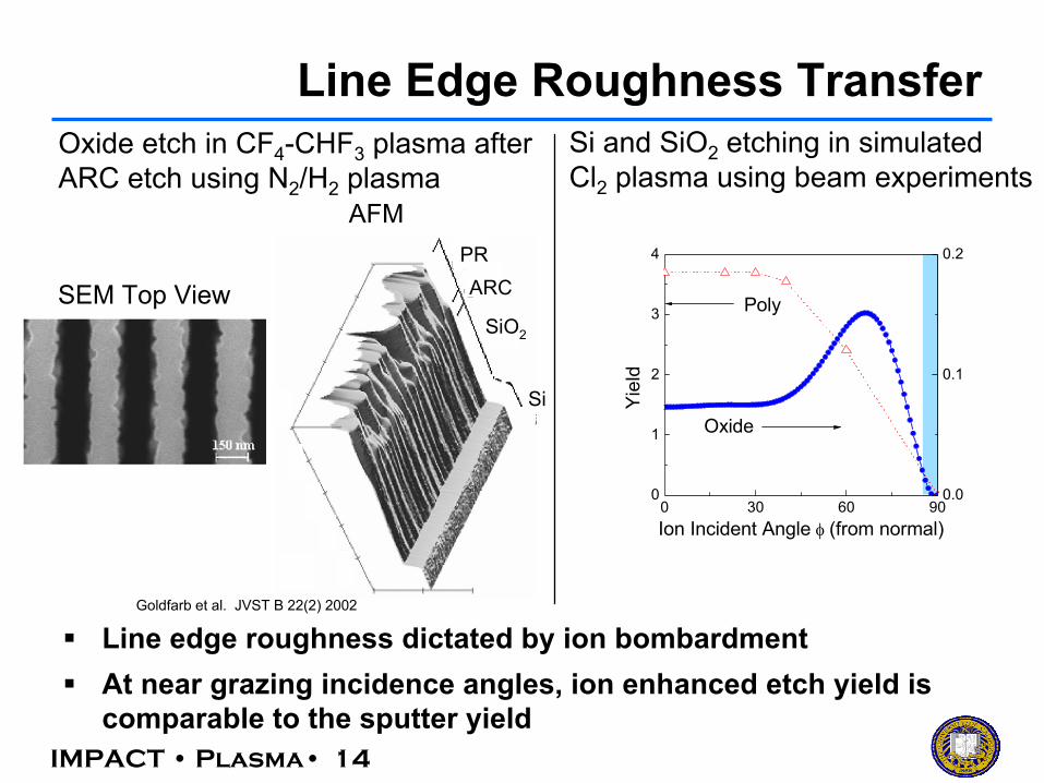
Line Edge Roughness Transfer
Line edge roughness (LER) is a major concern with the use of 193 nm (ArF) resistsLER degrades device performance, yield and reliabilityCountermeasures include litho/etch process optimization and the addition of pattern transfer layer
A. Asenov, S. Kaya, and A. R. Brown, IEEE TRANSACTIONS ON ELECTRON DEVICES, VOL. 50, NO. 5, MAY 2003
• IMPACT round-table discussion in the summer, led by C. Gabriel, stimulated lots of discussions, signifying the importance to understand and model LER
IMPACT • Plasma• 14
Line Edge Roughness Transfer
Line edge roughness dictated by ion bombardmentAt near grazing incidence angles, ion enhanced etch yield is comparable to the sputter yield
SEM Top View
AFM
Goldfarb et al. JVST B 22(2) 2002
PRARC
SiO2
Si
0 30 60 900
1
2
3
4
0.0
0.1
0.2
Yiel
d
Ion Incident Angle φ (from normal)
Poly
Oxide
Oxide etch in CF4-CHF3 plasma afterARC etch using N2/H2 plasma
Si and SiO2 etching in simulatedCl2 plasma using beam experiments

IMPACT • Plasma• 15
Overview of mechanismsLitho– Nonhomogeneous resist film—“soft” and “hard” patches– Dimensions (resist thickness and CD) are close to the size of
polymer aggregatesEtch– Factors: Ion bombardment, radicals, photons, electrons, heat,
polymer deposition, but also linewidth and spacewidth seem to matter
– Ions and radicals attack soft areas in resist mask, creating rough surface and edges that transfer down into underlying films
– Worse when etching thick films with strong bonds, like SiO2– Film stress, adhesion, and stress relief may also play a role
– Volume expansion from ion implantation into mask– Wafer heating and cooling in plasma– Polymers deposited on mask and feature sidewalls
C. Gabriel, Spansion, IMPACT presentation, May 2008.

IMPACT • Plasma• 16
Role of photoresist
Both 248 nm and 193 nm resists use chemical amplification to make up for the relatively low intensity of DUV light produced by the KrF and ArF lasersChemically amplified resists form “spongy” walls—photoacid diffusion and catalytic reaction form coiled polymer chains or polymer aggregates, leading to a roughened sidewall when developedThe developed resist is nonhomogeneous and likelyto be further roughened by the physical and chemical action of plasma etching
H. Namatsu et al., J. Vac. Sci. Technol. B 16, 6, 1998, 3315
C. Gabriel, Spansion, IMPACT presentation, May 2008.

IMPACT • Plasma• 17
Challenges in Modeling
Physics – Effect of ions – Synergistic effect with photons and electrons
Chemistry – Simple chemistry (halogen) – Complex chemistry (fluorocarbon)
Materials – Reaction kinetics

IMPACT • Plasma• 18
Ion Bombardment Induced Surface Roughness
Begins with nucleation which affects surface advancement and propagates
Nucleation Surface AdvancementInitial Surface
Smooth SiO2
1. Surface composition
3. Surface density2. Ion flux
SiO
FC
CFx+ ion
Caused by variations in: Caused by:
CFx+ ion
1. Angular dependence of etching
3. Scattering and shadowing2. Local curvature dependence
4. Redeposition of etch products

IMPACT • Plasma• 19
Ion Angular Dependence: Roughness Striation
Transverse roughness at 45~60° off normal incidenceParallel roughness >75° off normal incidence
Ziberi et al. Physical Review B 72, 235310 (2005)
Bradley et al. JVST A 6(4), 2390(1988)
Isotropic roughness
θ = 0°
Transverse roughness
θ = 45-60°
Parallel roughness
θ >75°
HRTEM/AFM Xe+ ion beam eroded Si surface
5° 45° 75°
Ion Angular Dependence on Roughness Striation
1200 eV ions, 1.34x1019 cm-2 fluence
2000 eV ions, 6.7x1018 cm-2 fluence

IMPACT • Plasma• 20
Ion Flux Dependence: Deposited Energy
Energy of ion bombardment is dissipated in an elliptical symmetry with high at centerEtching caused by ion striking surface at A is highest at BCurvature and ion incident angle affects deposited energy profile
P. Sigmund. J. Materi. Sci. 8, 1545 (1973)
contour of deposited energy
ion
AB
surface
θ
Slower etch rate forNegative curvature
Higher etch rate for positive curvature
Curvature and angle dependence on etch yield

IMPACT • Plasma• 21
Density Dependence
Films with larger pores roughen at earlier stages during etchingPore filling with polymeric deposits causes surface imhomogeneity
QMS Neutral Spectra
QMS Ion Spectra
C2F6/Ar plasma etch, 5 sccm, beam source pressure ~10 mT, rf source power 250 W
Solid organosilicate glass (OSG)
Porous methylsilsesquioxane (MSQ) low-k film
unetched
rms 0.9 nm
115 nm etch 300 nm etch
rms 3.2 nm rms 9.0 nm
unetched
rms 1.2 nm
97 nm etch 238 nm etch
rms 0.9 nm rms 1.1 nm
Yin, Y, Rasgon, S. and Sawin, H. H. JVST B 24(5) 2006
IMPACT • Plasma• 22
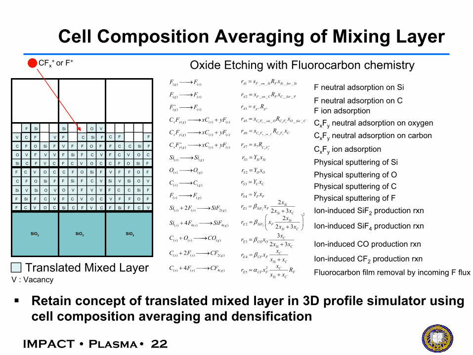
Cell Composition Averaging of Mixing Layer
Retain concept of translated mixed layer in 3D profile simulator using cell composition averaging and densification
Oxide Etching with Fluorocarbon chemistry( ) ( )
( ) ( )
( ) ( )
( ) ( ) ( )
( ) ( ) ( )
( ) ( ) ( )
( ) ( )
( ) ( )
( ) ( )
( ) ( )
( ) ( ) 2( )
( ) 4( ) 4( )
( ) ( )
2
4
g s
g s
g s
x y g s s
x y g s s
x y g s s
s g
s g
s g
s g
s s g
s s g
s s
F F
F F
F F
C F xC yF
C F xC yF
C F xC yF
Si Si
O O
C C
F F
Si F SiF
Si F SiF
C O C
+
+
→
→
→
→ +
→ +
→ +
→
→
→
→
+ →
+ →
+ → ( )
( ) ( ) 2( )
( ) ( ) 4( )
2
4
g
s s g
s s g
O
C F CF
C F CF
+ →
+ →
212
2 3Si
E SiF FSi C
xr xx x
β=+
F neutral adsorption on Si
F neutral adsorption on CF ion adsorptionCxFy neutral adsorption on oxygenCxFy neutral adsorption on carbon
CxFy ion adsorptionPhysical sputtering of SiPhysical sputtering of OPhysical sputtering of CPhysical sputtering of F
1 _ _ _ _A F on Si F Si for Sir s R x=
2 _ _ _ _A F on C F C for Fr s R x=
3A F Fr s R+ +=
5 _ _ _ _x y x yA C F on O C F O for Cr s R x=
_ _6 x y on C x yA C F C F Cr s R x=
7 7x y
A C Fr s R +=
1S Si Sir Y x=
2S O Or Y x=
3S C Cr Y x=
4S F Fr Y x=
2
2
22
2 3Si
E SiF FSi C
xr xx x
β
= +
33
2 3C
E CO OSi C
xr xx x
β=+
4C
E CF FSi C
xr xx x
β=+
25
CE CF F F
Si C
xr x Rx x
α=+
Ion-induced SiF2 production rxn
Ion-induced SiF4 production rxn
Ion-induced CO production rxn
Ion-induced CF2 production rxn
Fluorocarbon film removal by incoming F fluxTranslated Mixed Layer
SiO2
F Si
V C F V
C F O Si F
O V F V V
Si C F V C
Si O V
F C Si F
V F F O F
F Si F C V
F C V O C
C F F
F C C Si F
F C V O C
C F O Si F
C F O Si F
Si V Si O V
F Si F C V
F C V O C
F C V O C
F Si F C V
C F O Si F
O V F V V
V F F O F
F C V O C
Si C F V C
V F F O F
Si V Si O V
F C C Si F
F Si F C V
SiO2 SiO2
V : Vacancy
CFx+ or F+
IMPACT • Plasma• 23
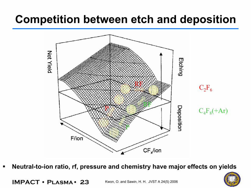
Competition between etch and deposition
Neutral-to-ion ratio, rf, pressure and chemistry have major effects on yields
Kwon, O. and Sawin, H. H. JVST A 24(5) 2006
C2F6
C4F8(+Ar)
RF
P RF
P
IMPACT • Plasma• 24
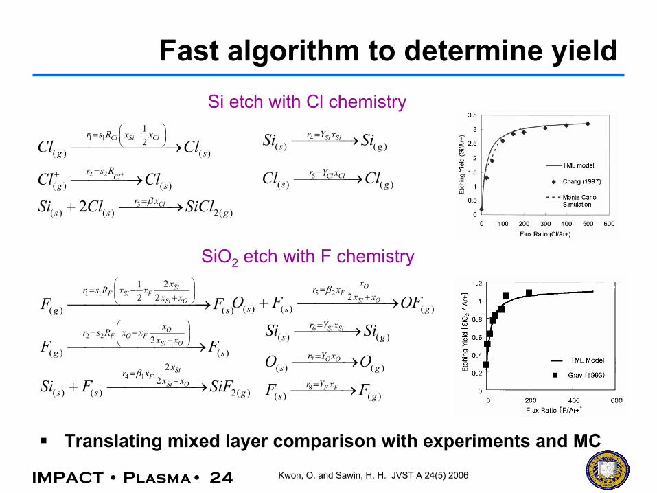
Fast algorithm to determine yield
Translating mixed layer comparison with experiments and MCKwon, O. and Sawin, H. H. JVST A 24(5) 2006
SiO2 etch with F chemistry
Si etch with Cl chemistry
1 112
( ) ( )
Cl Si Clr s R x x
g sCl Cl = − →
2 2
( ) ( )Cl
r s Rg sCl Cl+=+ →
3( ) ( ) 2( )2 Clr xs s gSi Cl SiClβ=+ →
4( ) ( )
Si Sir Y xs gSi Si=→
5( ) ( )
Cl Clr Y xs gCl Cl=→
1 121
2 2( ) ( )
SiF Si F
Si O
xr s R x x
x xg sF F
= − + →
2 2 2( ) ( )
OF O F
Si O
xr s R x x
x xg sF F
= − + →
4 12
2( ) ( ) 2( )
SiF
Si O
xr x
x xs s gSi F SiF
β=++ →
5 2 2( ) ( ) ( )
OF
Si O
xr x
x xs s gO F OF
β=++ →
6( ) ( )
Si Sir Y xs gSi Si=→
7( ) ( )
O Or Y xs gO O=→
8( ) ( )
F Fr Y xs gF F=→
IMPACT • Plasma• 25
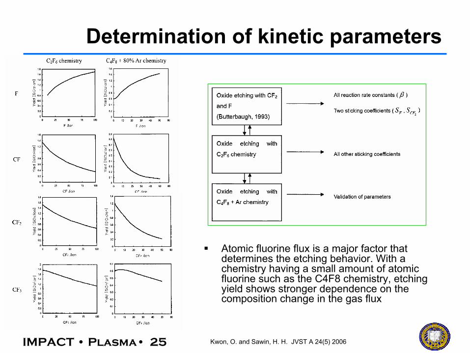
Determination of kinetic parameters
Atomic fluorine flux is a major factor that determines the etching behavior. With a chemistry having a small amount of atomic fluorine such as the C4F8 chemistry, etching yield shows stronger dependence on the composition change in the gas flux
Kwon, O. and Sawin, H. H. JVST A 24(5) 2006

IMPACT • Plasma• 26
Challenges in Modeling
Understand the effect of ions – Effect of relevant yet complex chemistry
Need to deconvolute the effect of dominant ions/radicals – Low ion energy reduces the LWR (R. Gottscho, 2008)– Ion energy can be controlled by frequency mix, pressure, bias
Need to determine the energy deposition on a shaped surfaceUnderstand the effect of photons/electrons – Wavelength and fluence– VUV flux and its ratio to ions
Need to quantify the reaction kinetics Expand the simulator into 3-D

IMPACT • Plasma• 27
Beam system 193 nm PR roughening S
imul
tane
ous
1x10
18io
ns·c
m-2
&2.
5x10
17ph
oton
s·cm
-21
1.52 2.17 3.5320ºC 40ºC 65ºC
1.32
10 nm
1.23
10 nm
1.02
10 nm
10 nm 10 nm 25 nm
1x10
18io
ns·c
m-2
ions
onl
y
200 nm
Elevated surface roughness on the order of plasmas exposures is observed during simultaneous ion bombardment, VUV radiation, and heatingThe surface roughness formation is photon/ion ratio dependent
VUV breaks C=O and C-O-C bonds (as verified by FTIR analysis)
150 eV Ar147 nm (Xe)
RMS of 0.3 nm for as-prepared and photon-radiated samples
D. Graves, UC Berkeley, IMPACT presentation, October 2008.

IMPACT • Plasma• 28
Translating Mixed-Layer Representation
• Robust kinetic model able to handle complex chemistries
Kwon, O. et al. JVST A 24(5) 2006
Cl2 Plasma Etch of Si
50100
150200
250
0.0
0.5
1.0
1.5
2.0
2.5
4060
80100
120140
Etc
h Yi
eld
n/I+ R
atioIon Energy (eV)
020
4060
80
0.0
0.5
1.0
1.5
10075
5025
0
Etc
h Yi
eld
n/I+ R
atio (
Total
)
Ion Incident Angle
C4F8 Plasma Etch of SiO2
0.150.20
0.250.30
0.35
0
1
2
3
0.12
0.140.16
0.18
Etch
Yie
ld
s Carbons
Flourine
400800
12001600
2000
-0.50.00.51.01.5
2.0
2.5
3.0
12090
6030
0
Etch
Yie
ld
n/I+ Ratio (T
otal)Ion Energy (eV)
020
4060
80
-2-10123456
040
80120
Etch
Yie
ld
n/I+ Ratio
Ion Incident Angle

IMPACT • Plasma• 29
Surface Algorithm
-Vacuum Cell
-Solid Reference Cell
-Solid Interface Cell
-Solid Inside cell
Steps:
1. Create “Quick Normal”
2. Locate interface cells around reference cell
3. Connect interface cells with “snaking”algorithm

IMPACT • Plasma• 30
Particle Intersection and Normal
Steps:
4. With particle trajectory and starting point, find intersection with a plane
5. Calculate surface normal
Reference Cell
IMPACT • Plasma• 31
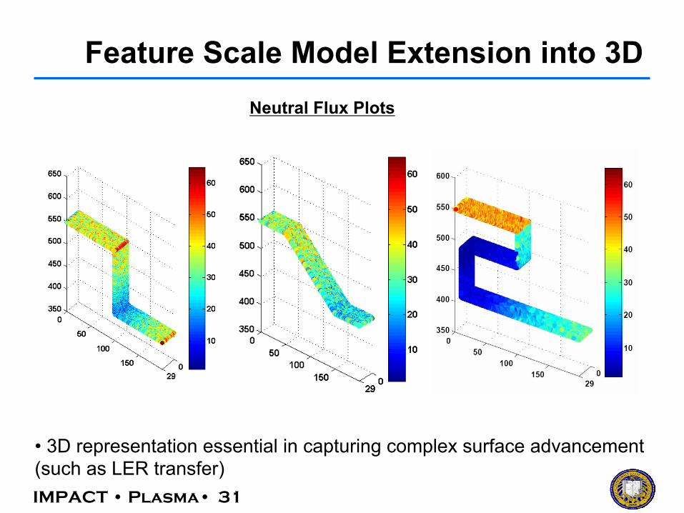
Feature Scale Model Extension into 3D
• 3D representation essential in capturing complex surface advancement (such as LER transfer)
Neutral Flux Plots

IMPACT • Plasma• 32
Potential Directions
• STIE with new chemistry (Spansion) • LER (AMD and Spansion) • TSV etch (Synopsis) • Gap-fill and Cu deposition (Novellus) • Scatterometry (Timbre)

IMPACT • Plasma• 33
Acknowledgement
UC IMPACTHerb Sawin, MIT (Equipment donation and software)