technology image...sii 163b panellink® receiver july 2005 data sheet sii-ds-0055-c general...
TRANSCRIPT

®
Technology
SiI 163B PanelLink Receiver
Data Sheet
Document # SiI-DS-0055-C

SiI 163B PanelLink Receiver Data Sheet
ii SiI-DS-0055-C
Silicon Image, Inc. SiI-DS-0055-C July 2005 Application Information To obtain the most updated Application Notes and other useful information for your design, please visit the Silicon Image web site at www.siimage.com, or contact your local Silicon Image sales office.
Copyright Notice This manual is copyrighted by Silicon Image, Inc. Do not reproduce, transform to any other format, or send/transmit any part of this documentation without the expressed written permission of Silicon Image, Inc.
Trademark Acknowledgment Silicon Image, the Silicon Image logo, PanelLink®, TMDS® and the PanelLink® Digital logo are registered trademarks of Silicon Image, Inc. VESA® is a registered trademark of the Video Electronics Standards Association. All other trademarks are the property of their respective holders.
Disclaimer This document provides technical information for the user. Silicon Image, Inc. reserves the right to modify the information in this document as necessary. The customer should make sure that they have the most recent data sheet version. Silicon Image, Inc. holds no responsibility for any errors that may appear in this document. Customers should take appropriate action to ensure their use of the products does not infringe upon any patents. Silicon Image, Inc. respects valid patent rights of third parties and does not infringe upon or assist others to infringe upon such rights.
All information contained herein is subject to change without notice.
Revision History Revision Date Comment SiI-DS-0055-A 03/02 Full Release SiI-DS-0055-B 08/04 Added ePad dimensions and Slave SCDT stabilization guideline. SiI-DS-0055-C 07/05 ePad dimensions fix. Part ordering number update.
© 2001-2005 Silicon Image. Inc.

SiI 163B PanelLink Receiver Data Sheet
iii SiI-DS-0055-C
TABLE OF CONTENTS
SiI 163B Pin Diagram ..................................................................................................................................... 1 Functional Description .................................................................................................................................... 2 Electrical Specifications .................................................................................................................................. 3
Absolute Maximum Conditions ................................................................................................................... 3 Normal Operating Conditions ..................................................................................................................... 3 Digital I/O Specifications ............................................................................................................................. 3 DC Specifications........................................................................................................................................ 4 AC Specifications ........................................................................................................................................ 5
Setup and Hold Timings for Data Rates other than 165 MHz................................................................. 6 Timing Diagrams............................................................................................................................................. 7 Pin Descriptions............................................................................................................................................ 10
Output Pins ............................................................................................................................................... 10 Configuration Pins..................................................................................................................................... 11 Power Management Pins.......................................................................................................................... 11 Differential Signal Data Pins ..................................................................................................................... 12 Reserved Pin............................................................................................................................................. 12 Power and Ground Pins............................................................................................................................ 12
Feature Information ...................................................................................................................................... 13 Dual Link ................................................................................................................................................... 13
Dual Link Configuration Pins................................................................................................................. 13 Dual Link Power Management .............................................................................................................. 16 Dual Link Mode Selection...................................................................................................................... 16 Dual Link Timing Diagrams ................................................................................................................... 17
Clock Detect Function............................................................................................................................... 19 OCK_INV# Function ................................................................................................................................. 19 TFT Panel Data Mapping.......................................................................................................................... 20
Design Recommendations ........................................................................................................................... 27 Differences Between SiI 161A and SiI 163B ............................................................................................. 27 Voltage Ripple Regulation......................................................................................................................... 28 Decoupling Capacitors.............................................................................................................................. 29 Series Damping Resistors on Outputs...................................................................................................... 30 Receiver Layout ........................................................................................................................................ 30 Stabilized TMDS Inputs............................................................................................................................. 32 Staggered Outputs and Two Pixels per Clock .......................................................................................... 32
Packaging ..................................................................................................................................................... 33 ePad Enhancement .................................................................................................................................. 33
PCB Thermal Land Area ....................................................................................................................... 34 100-pin TQFP Package Dimensions and Marking Specification .............................................................. 35 Marking Specification ................................................................................................................................ 35
Ordering Information..................................................................................................................................... 35

SiI 163B PanelLink Receiver Data Sheet
iv SiI-DS-0055-C
LIST OF TABLES
Table 1. Setup and Hold Times at Various Data Rates .................................................................................. 6 Table 2. SiI 163B Dual Link Pin Definitions.................................................................................................. 13 Table 3. SiI 163B Dual Link Pin Configuration............................................................................................. 15 Table 4. DVI-D Connector to SiI 163B for Dual Link Application Pin Connection........................................ 19 Table 5. One Pixel/Clock Mode Data Mapping............................................................................................. 20 Table 6. Two Pixel/Clock Mode Data Mapping ............................................................................................. 20 Table 7. One Pixel/Clock Input/Output TFT Mode – VESA P&D and FPDI-2TM Compliant.......................... 21 Table 8. Two Pixels/Clock Input/Output TFT Mode ...................................................................................... 22 Table 9. 24-bit One Pixel/Clock Input with 24-bit Two Pixels/Clock Output TFT Mode................................ 23 Table 10. 18-bit One Pixel/Clock Input with 18-bit Two Pixels/Clock Output TFT Mode.............................. 24 Table 11. Two Pixels/Clock Input with One Pixel/Clock Output TFT Mode .................................................. 25 Table 12. Output Clock Configuration by Typical Application ....................................................................... 26 Table 13. SiI 161A vs. SiI 163B Pin Differences ........................................................................................... 27 Table 14. SiI 161B vs. SiI 163B Pin Differences ........................................................................................... 27 Table 15. Recommended Components ........................................................................................................ 29
LIST OF FIGURES Figure 1. Functional Block Diagram ............................................................................................................... 2 Figure 2. Digital Output Transition Times ....................................................................................................... 7 Figure 3. Receiver Clock Cycle/High/Low Times ........................................................................................... 7 Figure 4. Channel-to-Channel Skew Timing .................................................................................................. 7 Figure 5. Output Setup/Hold Timings ............................................................................................................. 8 Figure 6. Output Signals Disabled Timing from Clock Inactive ...................................................................... 8 Figure 7. Wake-Up on Clock Detect ............................................................................................................... 8 Figure 8. Output Signals Disabled Timing from PD# Active ........................................................................... 8 Figure 9. SCDT Timing from DE Inactive or Active ........................................................................................ 9 Figure 10. Two Pixel per Clock Staggered Output Timing Diagram............................................................... 9 Figure 11. SiI 163B Dual Link Block Diagram .............................................................................................. 14 Figure 12. Timing Diagram of Master's Output............................................................................................. 17 Figure 13. Timing Diagram of Slave's Output............................................................................................... 18 Figure 14. Single/Dual Link Timing Diagram................................................................................................ 18 Figure 15. Block Diagram for OCK_INV#..................................................................................................... 19 Figure 16. Voltage Regulation using TL431 ................................................................................................. 28 Figure 17. Voltage Regulation using LM317 ................................................................................................ 28 Figure 18. Decoupling and Bypass Capacitor Placement............................................................................ 29 Figure 19. Decoupling and Bypass Schematic............................................................................................. 29 Figure 20. Receiver Output Series Damping Resistors ............................................................................... 30 Figure 21. DVI Dual Link Rx PCB Routing Example – Top View ................................................................. 30 Figure 22. DVI Dual Link Rx PCB Routing Example – Top Signals Top View.............................................. 31 Figure 23. DVI Dual Link Rx PCB Routing Example - Bottom Signals Top View......................................... 31 Figure 24. Stabilizing SCDT ......................................................................................................................... 32 Figure 25. ePad Diagram ............................................................................................................................. 33 Figure 26. ePad Template Layout................................................................................................................. 34 Figure 27. Package Dimensions and Marking Specification ........................................................................ 35

SiI 163B PanelLink® Receiver July 2005 Data Sheet
SiI-DS-0055-C
General Description Features The SiI 163B receiver uses PanelLink Digital technology to support high-resolution (24 bit/pixel, 16M colors) displays up to UXGA and beyond, with dual-link DVI for a total bandwidth up to 330 megapixels per second.
All PanelLink products are designed on a scaleable CMOS architecture, ensuring support for future performance enhancements while maintaining the same logical interface. System designers can be assured that the interface will be stable through a number of technology and performance generations.
PanelLink Digital technology simplifies PC and display interface design by resolving many of the system level issues associated with high-speed mixed signal design, providing the system designer with a digital interface solution that is quicker to market and lower in cost.
• Low Power Operation: 280mA max. current consumption at 3.3V core operation
• Sync Detect feature for Plug & Display “Hot Plugging”
• Cable Distance Support: over 5m with twisted-pair, fiber-optics ready
• Compliant with DVI 1.0 • Low power standby mode • Automatic entry into standby mode with clock
detect circuitry • Dual-Link DVI support with two devices
configured as master and slave
SiI 163B Pin Diagram
S_D1
SiI 163B100 -Pin TQFP
(Top View)
PD#2
ST3
PIXS/M_S4
GND5
VCC6
STAG_OUT#/SYNC7
SCDT8
PDO#9
QE010
QE111
QE212
QE313
QE414
QE515
QE616
QE717
OVCC18
OGND19
QE820
QE921
QE1022
QE1123
QE1224
QE1325
QE
1426
QE
1527
OG
ND
28
OV
CC
29
QE
1630
QE
1731
QE
1832
QE
1933
QE
2034
QE
2135
QE
2236
QE
2337
VC
C38
GN
D39
CTL
140
CTL
241
CTL
342
OV
CC
43
OD
CK
44
OG
ND
45
DE
46
VS
YN
C47
HS
YN
C48
QO
049
QO
150
75
QO21 74
QO20 73
QO19 72
QO18 71
QO17 70
QO16 69
GND 68
VCC 67
QO15 66
QO14 65
QO13 64
QO12 63
QO11 62
QO10 61
QO9 60
QO8 59
OGND 58
OVCC 57
QO7 56
QO6 55
QO5 54
QO4 53
QO3 52
QO2 51
QO22
OC
K_I
NV
#10
0
RE
SE
RV
ED
99
PG
ND
98
PV
CC
97
EX
T_R
ES
96
AV
CC
95
RX
C-
94
RX
C+
93
AG
ND
92
RX
0-91
RX
0+90
AG
ND
89
AV
CC
88
AG
ND
87
RX
1-86
RX
1+85
AV
CC
84
AG
ND
83
AV
CC
82
RX
2-81
RX
2+80
AG
ND
79
OV
CC
78
QO
2377
OG
ND
76
DIFFERENTIAL SIGNAL
OD
D 8
-bits
RE
D
EVEN 8-bits RED
OD
D 8
-bits
GR
EE
N
EV
EN
8-b
its G
RE
EN
OD
D 8
-bits
BLU
E
EV
EN
8-b
its B
LUE
CO
NFI
G. P
INS
PLL
PW
RM
AN
AG
EM
EN
T
GPOOU
TPU
T C
LOC
K
CONTROLS

SiI 163B PanelLink Receiver Data Sheet
2 SiI-DS-0055-C
Functional Description The SiI 163B is a DVI 1.0 compliant PanelLink receiver in a compact package. It provides 48 bits for data output to allow for panel support up to UXGA and dual-link applications. Figure 1 shows the functional blocks of the chip.
PLL
TerminationControl
ChannelSYNC
Data RecoveryCH2
Data RecoveryCH0
Data RecoveryCH1
VCR
PanelInterface
Logic
RX2+
RX2-
RXC+
RXC-
RX0+
RX0-
RX1+
RX1-
PDO#STAG_OUT#
/SYNCST
EXT_RES
OCK_INV#
S_D
PIXS/M_S
VCR
VCR
VCR
SYNC2
SYNC1
SYNC0
Decoder
QE[23:0]
QO[23:0]
ODCKDE
HSYNCVSYNC
SCDTCTL[3:1]
Figure 1. Functional Block Diagram
The PanelLink TMDS core accepts as inputs the three TMDS differential data lines and the differential clock. The core senses the signals on the link and properly decodes them providing accurate pixel data. The core outputs the necessary sync signals (HSYNC, VSYNC), clock (ODCK), and a DE signal that goes high when the active region of the video is present.
The SCDT signal is output when there is active video on the DVI link and the PLL in the TMDS has locked on to the video. SCDT can be used to trigger external circuitry, indicating that an active video signal is present or used to place the device in power down when no signal is present (by tying it to PD#). The EXT_RES component is used for impedance matching.
When Single/Dual Link Mode (S_D) is HIGH, the signals M_S and SYNC are used to select and coordinate operation of two receivers in a dual-link DVI configuration. In this mode, at frequencies up to 165 MHz, the master receiver outputs two pixels/clock (48 data bits). At frequencies above 165 MHz, the master outputs even pixels (24 bits) while the slave receiver outputs odd pixels (24 bits) synchronized with one DE output from the master.

SiI 163B PanelLink Receiver Data Sheet
3 SiI-DS-0055-C
Electrical Specifications
Absolute Maximum Conditions Symbol Parameter Min Typ Max Units
VCC Supply Voltage 3.3V (note 1) -0.3 4.0 V VI Input Voltage -0.3 VCC+ 0.3 V VO Output Voltage (note 2) -0.3 VCC+ 0.3 V TJ Junction Temperature 125 °C
TSTG Storage Temperature -65 150 °C Notes
1. Permanent device damage may occur if absolute maximum conditions are exceeded. 2. Functional operation should be restricted to the conditions described under Normal Operating Conditions.
Normal Operating Conditions Symbol Parameter Min Typ Max Units
VCC Supply Voltage 3.0 3.3 3.6 V VCCN Supply Voltage Noise 100 mVP-P TA Ambient Temperature (with power applied) 0 25 70 °C θJA Thermal Resistance
Junction to Ambient – ePad soldered 21 °C/W
θJAU Thermal Resistance Junction to Ambient – ePad unsoldered
30 °C/W
Silicon Image recommends soldering of ePad to improve thermal performance, especially at highest speeds.
Note 1. θJA value based on 100% soldered down on multi-layer board.
Digital I/O Specifications Under normal operating conditions unless otherwise specified.
Symbol Parameter Conditions Min Typ Max Units VIH High-level Input Voltage 2 V VIL Low-level Input Voltage 0.8 V VOH High-level Output Voltage 2.4 V VOL Low-level Output Voltage 0.4 V
VCINL Input Clamp Voltage1 ICL = -18mA GND -0.8 V VCIPL Input Clamp Voltage1 ICL = 18mA IVCC + 0.8 V VCONL Output Clamp Voltage1 ICL = -18mA GND -0.8 V VCOPL Output Clamp Voltage1 ICL = 18mA OVCC + 0.8 V
IOL Output Leakage Current High Impedance -10 10 µA Note
1. Guaranteed by design. Voltage undershoot or overshoot cannot exceed absolute maximum conditions for a pulse of greater than 3 ns or one third of the clock cycle.

SiI 163B PanelLink Receiver Data Sheet
4 SiI-DS-0055-C
DC Specifications Under normal operating conditions unless otherwise specified.
Symbol Parameter Conditions Min Typ Max Units IOHD Output High Drive Data and
Controls VOUT = 2.4 V; ST = 1 ST = 0
7.4 3.8
12.6 6.4
18.2 9.2
mA
IOLD Output Low Drive Data and Controls
VOUT = 0.8 V; ST = 1 ST = 0
-11.1 -5.5
-12.6 -6.4
-13.6 -6.9
mA
VOUT = 0.4 V; ST = 1 ST = 0
-6.3 -3.2
-6.9 -3.5
-7.6 -3.8
mA
IOHC ODCK, DE High Drive VOUT = 2.4 V; ST = 1 ST = 0
14.7 7.5
23.8 11.5
34.3 17.6
mA
IOLC ODCK, DE Low Drive VOUT = 0.8V; ST = 1 ST = 0
-21.2 -11.1
-26.7 -12.5
-27.5 -13.9
mA
VOUT = 0.4 V; ST = 1 ST = 0
-12.3 -6.2
-13.6 -6.8
-15.9 -7.6
mA
VID Differential Input Voltage Single Ended Amplitude
75 1000 mV
IPD Power-down Current PD#=LOW, No RXC+ input 1 mA ICLKI Power-down Current PD#=HIGH, No RXC+ input 3 mA IPDO Receiver Supply Current with
Outputs Powered Down ODCK=87.5 MHz, 2-pixel/clock mode CLOAD = 10pF REXT_SWING = 510 ohm PDO# = LOW
133 mA
ICCR Receiver Supply Current
ODCK=87.5 MHz, 2-pixel/clock mode CLOAD= 10pF REXT_SWING = 510 ohm Typical Pattern1
240 mA
ODCK=87.5 MHz, 0°C 2-pixel/clock mode CLOAD = 10pF REXT_SWING = 510 ohm Worst Case Pattern2
280 mA
Notes 1. The Typical Pattern contains a gray scale area, checkerboard area, and text. 2. The Worst Case Pattern consists of a black and white checkerboard pattern; each checker is two pixels wide.

SiI 163B PanelLink Receiver Data Sheet
5 SiI-DS-0055-C
AC Specifications Under normal operating conditions unless otherwise specified.
Symbol Parameter Conditions Min Typ Max Units TDPS Intra-Pair (+ to -) Differential Input Skew1 165MHz 245 ps TCCS Channel to Channel Differential Input Skew1 165MHz 4 ns TIJIT Worst Case Differential Input Clock Jitter 65 MHz 465 ps
tolerance2,3 112 MHz 270 ps 165 MHz 182 ps
DLHT CL = 10pF; ST = 1 2.6 ns
Low-to-High Transition Time: Data and Controls (70°C, 87.5 MHz, 2-pixel/clock, PIXS=1) CL = 5pF; ST = 0 2.7 ns
CL = 10pF; ST = 1 2.4 ns
Low-to-High Transition Time: Data and Controls (70°C, 165 MHz, 1-pixel/clock, PIXS=0) CL = 5pF; ST = 0 3.0 ns
CL = 10pF; ST = 1 1.3 ns
Low-to-High Transition Time: ODCK (70°C, 87.5 MHz, 2-pixel/clock, PIXS=1) CL = 5pF; ST = 0 1.7 ns
CL = 10pF; ST = 1 1.4 ns
Low-to-High Transition Time: ODCK (70°C, 165 MHz, 1-pixel/clock, PIXS=0) CL = 5pF; ST = 0 1.7 ns
DHLT CL = 10pF; ST = 1 2.8 ns
High-to-Low Transition Time: Data and Controls (70°C, 87.5 MHz, 2-pixel/clock, PIXS=1) CL = 5pF; ST = 0 3.4 ns
CL = 10pF; ST = 1 2.3 ns
High-to-Low Transition Time: Data and Controls (70°C, 165 MHz, 1-pixel/clock, PIXS=0) CL = 5pF; ST = 0 3.3 ns
CL = 10pF; ST = 1 1.1 ns
High-to-Low Transition Time: ODCK (70°C, 87.5 MHz, 2-pixel/clock, PIXS=1) CL = 5pF; ST = 0 1.5 ns
CL = 10pF; ST = 1 1.2 ns
High-to-Low Transition Time: ODCK (70°C, 165 MHz, 1-pixel/clock, PIXS=0) CL = 5pF; ST = 0 1.5 ns
TSETUP CL = 10pF; ST = 1 0.9 (1.4)6
ns
Data, DE, VSYNC, HSYNC, and CTL[3:1] Setup Time to ODCK falling edge (OCK_INV# = 0) or to ODCK rising edge (OCK_INV# = 1) at 165 MHz CL = 5pF; ST = 0 0.7
(0.5)6 ns
THOLD CL = 10pF; ST = 1
2.7 (2.3)6
ns
Data, DE, VSYNC, HSYNC, and CTL[3:1] Hold Time from ODCK falling edge (OCK_INV# = 0) or from ODCK rising edge (OCK_INV# = 1) at 165 MHz CL = 5pF; ST = 0 3.0
(2.6)6 ns
RCIP ODCK Cycle Time1 (1-pixel/clock) 6.06 40 ns FCIP ODCK Frequency1 (1-pixel/clock) 25 165 MHz RCIP ODCK Cycle Time1 (2-pixels/clock) 12.1 80 ns FCIP ODCK Frequency1 (2-pixels/clock) 12.5 82.5 MHz RCIH CL = 10pF; ST = 1 1.7 ns
ODCK High Time4
CL = 5pF; ST = 0 1.3 ns RCIL CL = 10pF; ST = 1 2.0 ns
ODCK Low Time4
165 MHz, 1 pixel/clock, PIXS=0.
CL = 5pF; ST = 0 1.4 ns TPDL Delay from PD# / PDO# Low to high impedance outputs1 10 ns THSC Link disabled (DE inactive) to SCDT low1 100 ms
Link disabled (Tx power down) to SCDT low5 250 ms TFSC Link enabled (DE active) to SCDT high1 25 40 DE edges
TCLKPD Delay from RXC+ Inactive to high impedance outputs RXC+ = 25MHz 10 µs TCLKPU Delay from RXC+ active to data active RXC+ = 25MHz 100 µs
TST ODCK high to even data output1 0.25 RCIP TOSK Output Skew from Slave to Master Data buses7 165 MHz 300 300 ps

SiI 163B PanelLink Receiver Data Sheet
6 SiI-DS-0055-C
Notes on previous table:
1. Guaranteed by design.
2. Jitter defined per DVI 1.0 Specification, Section 4.6 – Jitter Specification.
3. Jitter measured with Clock Recovery Unit per DVI 1.0 Specification, Section 4.7 – Electrical Measurement Procedures.
4. Output clock duty cycle is independent of the differential input clock duty cycle and the IDCK duty cycle.
5. Measured with transmitter powered down.
6. Value in parentheses is specified with OCK_INV#=1.
7. Skew between output data buses when two SiI 163B are wired in master-slave configuration for dual-link. See the Receiver Layout section on page 30. The ‘minimum’ is the limit of Slave leading Master (slave data output earlier than master data). The ‘maximum’ is the limit of Slave lagging Master (slave data output later than master data). When the Slave lags the Master, then the setup time available from Slave data to ODCK (from the Master) is reduced.
Setup and Hold Timings for Data Rates other than 165 MHz The measurements shown above are minimum setup and hold timings based on the maximum data rate of 165 MHz. To estimate the setup and hold times for slower data rates (for either different resolutions or 2 pixel per clock mode), the following formula can be used:
Time (at new frequency) = Time (165 MHz) + (Clock Period at new frequency – Clock Period at 165 MHz)/2
For the case of high strength output (ST=1) with a 10pf load, and using the standard ODCK (OCK_INV# = 0), Table 1 shows the minimum set up and hold times for other speeds as follows:
Table 1. Setup and Hold Times at Various Data Rates Data Rate (MHz) Clock (ns) Setup (ns) Hold (ns)
112 56
8.9 17.9
2.3 6.8
4.1 8.6
SXGA 1 pixel/clock SXGA 2 pixels/clock
135 7.4 1.6 3.4 SXGA+ 1 pixel/clock 67.5 82.5
14.8 12.1
5.3 3.9
7.1 5.7
SXGA+ 2 pixels/clock UXGA 2 pixels/clock
Designers may want to check whether OCK+INV#=0 or OCK_INV#=1 provides better setup and hold time margin for their dual-link design. If Slave data lags Master data, which is in part determined by the layout, then the setup time from Slave to clock may be reduced, and the opposite ODCK edge may be more useful.

SiI 163B PanelLink Receiver Data Sheet
7 SiI-DS-0055-C
Timing Diagrams
10pF / 5pFSiI 163B
DLHT D HLT
2.0 V 2.0 V
0.8 V 0.8 V
Figure 2. Digital Output Transition Times
Note: 1. 10pF loading used at ST=1 and 5pF loading using at ST=0
RCIH
RCIL
RCIP
2.0 V
0.8 V0.8 V
2.0 V 2.0 V
Figure 3. Receiver Clock Cycle/High/Low Times
RX0
RX1
RX2
T CCS
V DIFF=0V
VDIFF=0V
Figure 4. Channel-to-Channel Skew Timing

SiI 163B PanelLink Receiver Data Sheet
8 SiI-DS-0055-C
Output Timing
OCK_INV# = 1
OCK_INV# = 0
QE[23:0], QO[23:0],DE, CTL[3:1],
VSYNC, HSYNC
THOLDTSETUP
Figure 5. Output Setup/Hold Timings Note 1. Output Data, DE and Control Signals Setup/Hold Times – to ODCK Falling Edge when OCK_INV# = 0, or to ODCK
Rising Edge when OCK_INV# = 1. 2. See also the description of layout guidelines which guarantee limited skew between master and slave outputs in the
Receiver Layout section on page 30.
Figure 6. Output Signals Disabled Timing from Clock Inactive
Figure 7. Wake-Up on Clock Detect
TPDL
QE[23:0], QO[23:0],DE, CTL[3:1],
VSYNC, HSYNC
PD#VIL
Figure 8. Output Signals Disabled Timing from PD# Active
RXC+
SCDT
TCLKPU + TFSC
RXC+
Q[35:0], DE,VSYNC, HSYNC,CTL[3:1]
TCLKPD
......
SiI 163B PanelLink Receiver Data Sheet
9 SiI-DS-0055-C
DE
SCDT
DE
SCDT
TTFSC
TTHSC
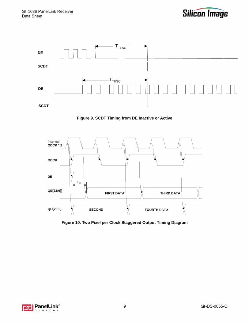
Figure 9. SCDT Timing from DE Inactive or Active
ODCK
DE
QE[23:0]]
QO[23:0]
FIRST DATA THIRD DATA
Internal ODCK * 2
SECOND FOURTH DATA
T ST
Figure 10. Two Pixel per Clock Staggered Output Timing Diagram

SiI 163B PanelLink Receiver Data Sheet
10 SiI-DS-0055-C
Pin Descriptions Output Pins
Pin Name
Pin # Type Description
QE23- QE0
See SiI 163B
Pin Diagram
Out Output Even Data[23:0]. Refer to the Dual Link section on page 13 for details. Output data is synchronized with output data clock (ODCK). Refer to the TFT Panel Data Mapping section on page 20, which tabulates the relationship between the input data to the transmitter and output data from the receiver. A low level on PD# or PDO# will put the output drivers into a high impedance (tri-state) mode. A weak internal pull-down device brings each output to ground.
QO23- QO0
See SiI 163B
Pin Diagram
Out Output Odd Data[23:0]. Refer to the Dual Link section on page 13 for details. Output data is synchronized with output data clock (ODCK). Output data is synchronized with output data clock (ODCK). Refer to the TFT Panel Data Mapping section on page 20, which tabulates the relationship between the input data to the transmitter and output data from the receiver. A low level on PD# or PDO# will put the output drivers into a high impedance (tri-state) mode. A weak internal pull-down device brings each output to ground.
ODCK 44 Out Output Data Clock. This output can be inverted using the OCK_INV# pin. A low level on PD# or PDO# will put the output driver into a high impedance (tri-state) mode. A weak internal pull-down device brings the output to ground.
DE 46 Out Output Data Enable. This signal qualifies the active data area. A HIGH level signifies active display time and a LOW level signifies blanking time. This output signal is synchronized with the output data. A low level on PD# or PDO# will put the output driver into a high impedance (tri-state) mode. A weak internal pull-down device brings the output to ground.
HSYNC VSYNC CTL1 CTL2 CTL3
48 47 40 41 42
Out Out Out Out Out
Horizontal Sync input control signal. Vertical Sync input control signal. General output control signal 1. This output is not powered down by PDO#. General output control signal 2. General output control signal 3. A low level on PD# or PDO# will put the output drivers (except CTL1 by PDO#) into a high impedance (tri-state) mode. A weak internal pull-down device brings each output to ground.
SiI 163B PanelLink Receiver Data Sheet
11 SiI-DS-0055-C
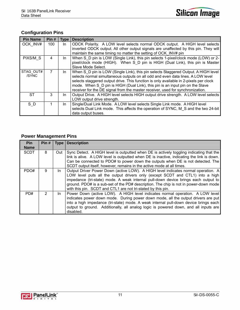
Configuration Pins Pin Name Pin # Type Description OCK_INV# 100 In ODCK Polarity. A LOW level selects normal ODCK output. A HIGH level selects
inverted ODCK output. All other output signals are unaffected by this pin. They will maintain the same timing no matter the setting of OCK_INV# pin
PIXS/M_S 4 In When S_D pin is LOW (Single Link), this pin selects 1-pixel/clock mode (LOW) or 2-pixel/clock mode (HIGH). When S_D pin is HIGH (Dual Link), this pin is Master Slave Mode Select.
STAG_OUT#/SYNC
7 In When S_D pin is LOW (Single Link), this pin selects Staggered Output. A HIGH level selects normal simultaneous outputs on all odd and even data lines. A LOW level selects staggered output drive. This function is only available in 2-pixels per clock mode. When S_D pin is HIGH (Dual Link), this pin is an input pin on the Slave receiver for the DE signal from the master receiver, used for synchronization.
ST 3 In Output Drive. A HIGH level selects HIGH output drive strength. A LOW level selects LOW output drive strength.
S_D 1 In Single/Dual Link Mode. A LOW level selects Single Link mode. A HIGH level selects Dual Link mode. This affects the operation of SYNC, M_S and the two 24-bit data output buses.
Power Management Pins Pin
Name Pin # Type Description
SCDT 8 Out Sync Detect. A HIGH level is outputted when DE is actively toggling indicating that the link is alive. A LOW level is outputted when DE is inactive, indicating the link is down. Can be connected to PDO# to power down the outputs when DE is not detected. The SCDT output itself, however, remains in the active mode at all times.
PDO# 9 In Output Driver Power Down (active LOW). A HIGH level indicates normal operation. A LOW level puts all the output drivers only (except SCDT and CTL1) into a high impedance (tri-state) mode. A weak internal pull-down device brings each output to ground. PDO# is a sub-set of the PD# description. The chip is not in power-down mode with this pin. SCDT and CTL1 are not tri-stated by this pin.
PD# 2 In Power Down (active LOW). A HIGH level indicates normal operation. A LOW level indicates power down mode. During power down mode, all the output drivers are put into a high impedance (tri-state) mode. A weak internal pull-down device brings each output to ground. Additionally, all analog logic is powered down, and all inputs are disabled.

SiI 163B PanelLink Receiver Data Sheet
12 SiI-DS-0055-C
Differential Signal Data Pins Pin Name Pin # Type Description
RX0+ RX0- RX1+ RX1- RX2+ RX2-
90 91 85 86 80 81
Analog Analog Analog Analog Analog Analog
TMDS Low Voltage Differential Signal input data pairs.
RXC+ RXC-
93 94
Analog Analog
TMDS Low Voltage Differential Signal input clock pair.
EXT_RES 96 Analog Impedance Matching Control. An external 390 ohm resistor must be connected between AVCC and this pin.
Reserved Pin Pin Name Pin # Type Description
RESERVED 99 In Must be tied HIGH for normal operation.
Power and Ground Pins Pin Name Pin # Type Description
VCC 6,38,67 Power Digital Core VCC, must be set to 3.3V. GND 5,39,68 Ground Digital Core GND.
OVCC 18,29,43,57,78 Power Output VCC, must be set to 3.3V. OGND 19,28,45,58,76 Ground Output GND. AVCC 82,84,88,95 Power Analog VCC must be set to 3.3V. AGND 79,83,87,89,92 Ground Analog GND. PVCC 97 Power PLL Analog VCC must be set to 3.3V. PGND 98 Ground PLL Analog GND.

SiI 163B PanelLink Receiver Data Sheet
13 SiI-DS-0055-C
Feature Information The SiI 163B can be configured in two modes: Single Link and Dual Link. When in Single Link (S_D is LOW), the device operates in either 1-pixel/clock or 2-pixel/clock mode, according to the state of the PIXS pin. There is no communication with a second receiver. In this mode, the SiI 163B operates in the same way as the other PanelLink receivers: SiI 143B, SiI 151B, SiI 153B and SiI 161B.
In Dual Link mode, two SiI 163B’s operate together to handle bandwidths up to 330 megapixels per second. The configuration and management of this mode is detailed in the following sections. Dual Link mode may operate across a pixel frequency of 25 MHz to 330 MHz. Below 165 MHz, the second TMDS channel is quiescent. All pixel data is sent across the first TMDS channel, and handled by the Master SiI 163B receiver. Above 165 MHz, both SiI 163B receivers are active, with the pixels alternating even-and-odd from Master to Slave, driven by the two TMDS DVI channels.
Dual Link Two SiI 163B’s are required for a DVI compatible Dual Link application as configured in the block diagram of Figure 11. At pixel frequencies up to 165 MHz, the system does not send any data over the second link connected to the Slave receiver. Therefore, the Slave receiver is not active and its outputs are tri-stated. All the data, both EVEN and ODD pixels, are sent over the TMDS link connected to the Master receiver. Therefore all the data, both EVEN and ODD pixels, is output by the Master receiver. At pixel frequencies above 165 MHz, the system sends EVEN data over the link connected to the Master receiver and the ODD data over the link connected to the Slave receiver. Therefore, the EVEN data is output by the Master receiver and the ODD data is output by the Slave receiver. The Master receiver’s ODD data bus is tri-stated to allow the Slave receiver’s EVEN Data bus to output the ODD data. Dual Link Configuration Pins Five pins on the SiI 163B need to be considered for Dual Link receiver applications.
Table 2. SiI 163B Dual Link Pin Definitions Pin Name Pin # Type Description
S_D 1 In Single/Dual Link Mode. When HIGH, it is in Dual Link Mode. When LOW it is in Single Link Mode. The Slave receiver is always in Dual Link mode. The Master receiver switches between Single and Dual Link mode depending upon the SCDT output of the Slave receiver that is connected to the S_D input of the Master receiver.
PIXS / M_S 4 In Master/Slave. When S_D pin is HIGH (Dual Link), this pin becomes M_S. When HIGH, it is in Master mode. When LOW, it is in Slave mode. The Master receiver is in one/two-pixels per clock mode depending upon Single/Dual Link operation. The Slave receiver is always in one-pixel per clock mode. When S_D is LOW (Single Link), this pin becomes PIXS.
STAG_OUT / SYNC
7 In Synchronization. When S_D pin is HIGH (Dual Link), this pin is used to synchronize the Slave receiver to the Master receiver. The SYNC input pin of the Slave receiver is connected to the DE output pin of the Master receiver.
SCDT 8 Out Sync Detect. When HIGH, there are valid sync signals coming from the transmitter. When LOW, there are no sync signals coming from the transmitter. The SCDT pin of the Slave receiver is connected to the S_D pin of the Master receiver.
DE 46 Out Data Enable. This signal qualifies the active data area. A HIGH level signifies active display time and a LOW level signifies blanking time. This output signal is synchronized with the output data. The DE output pin of the Master is connected to the SYNC input pin of the Slave.

SiI 163B PanelLink Receiver Data Sheet
14 SiI-DS-0055-C
163B Master
RX[3:1]
SCD
T
SYN
C
S_D
M_S DE
QO[23:0]
QE[23:0]
VSYNC
HSYNC
ODCK
PD
O#
RxC+/-
163B Slave
RX[3:1]
SC
DT
SY
NC
S_D
M_S DE
QO[23:0]
QE[23:0]
VSYNC
HSYNC
ODCK
PDO
#
RxC+/-
VCC
DE
QO[23:0]
QE[23:0]
VSYNC
HSYNC
ODCK
N/C
N/C
N/C
N/C
N/C
PDO#
TX1[3:1]
TX2[3:1]
TXC+/-
GN
DN
/C
SCDT
VCC
Figure 11. SiI 163B Dual Link Block Diagram

SiI 163B PanelLink Receiver Data Sheet
15 SiI-DS-0055-C
Master –
The Master receiver will automatically configure to either Single or Dual Link operation (two or one pixel per clock mode, respectively) depending on the transmitter system output. This is accomplished by connecting the SCDT output pin of the Slave to the S_D pin on the Master. When the transmitter sends data on the second link, the SCDT output of the slave (and the S_D pin on the Master) is driven HIGH, setting to Dual Link (one-pixel per clock) mode. If there is no data on the second link, the SCDT output of the Slave (and the S_D pin on the Master) is driven LOW, and the Master receiver is in Single Link (two-pixels per clock) mode.
The Master receiver is configured by pulling the M_S pin to HIGH. When it is in Dual Link mode, the Master receiver is in one-pixel per clock mode outputting the EVEN data. The Master receiver’s ODD data bus is tri-stated to allow the Slave receiver’s EVEN data bus to be used as the ODD data bus. When it is in Single Link mode, the Master receiver is in two-pixels per clock mode outputting both the EVEN and ODD data. The Slave receiver’s EVEN data bus is tri-stated to allow the Master receiver’s ODD data bus to be used as the ODD data.
The DE output pin of the Master receiver is connected to the SYNC input pin of the Slave receiver. This is used for output synchronization between the Master receiver and Slave receiver. DE, HSYNC, VSYNC, and ODCK are all connected from the Master receiver.
Slave – The Slave receiver is always configured for Dual Link (one pixel/clock) operation, by tying the S_D pin to HIGH. The Slave receiver is never used in Single Link mode since the Master receiver is the primary receiver for Single Link Operation.
The Slave receiver is configured by tying the M_S pin to LOW. The Slave receiver will always contain the ODD data bus in Dual Link operation. Therefore, it will never be in two-pixels per clock mode.
The SCDT output pin of the Slave receiver is connected to the S_D input pin of the Master receiver to automatically configure the Master for either Single or Dual Link mode depending upon whether the Slave receiver is active or not.
The SYNC input pin of the Slave receiver is connected to the DE output pin of the Master receiver for synchronization.
Since DE, HSYNC, VSYNC, and ODCK are all taken from the Master receiver, these pins are not connected from the Slave receiver.
Table 3. SiI 163B Dual Link Pin Configuration
S_D PIXS/M_S Master / Slave Description 0 0 Not Used Single Link One Pixel/Clock Mode. Not supported. 0 1 Master Single Link Two Pixel/Clock Mode. This is the mode that the Master
receiver will be in when in Single Link mode for pixel clock frequencies less than or equal to 165MHz.
1 0 Slave Dual Link Slave (One Pixel/Clock) Mode. This is the mode that the Slave receiver will always be in for pixel clock frequencies greater than 165MHz and less than 330MHz.
1 1 Master Dual Link Master (One Pixel/Clock) Mode. This is the mode that the Master receiver will be in when in Dual Link mode for pixel clock frequencies greater than 165MHz and less than 330MHz.

SiI 163B PanelLink Receiver Data Sheet
16 SiI-DS-0055-C
Dual Link Power Management
Power management with PD# and PDO# is slightly different in a Dual Link design than a Single Link. When the receivers are in dual-link mode (S_D=1), then the connection from SCDT to PDO# is internal. A receiver which detects no activity at the TMDS inputs will deassert SCDT, which will then put that chip into power-down-output mode. This is the process which enables the slave receiver to tri-state its outputs whenever it stops receiving data.
The outputs may also be directly tri-stated by asserting the PDO# pin.
Receivers will also enter a low-power state when the differential TMDS clock stops. The receiver awakens when the clock resumes, at which point the receiver begins checking for active data. Active data will assert SCDT and put the chip back into full-power mode.
Dual Link Mode Selection Single Link Mode –
In Single Link mode, the Slave receiver is not active. Its outputs are all tri-stated. The Slave receiver will detect that there is no signal coming from the transmitter and de-assert SCDT to LOW. The SCDT pin from the Slave receiver is connected to the Master receiver’s S_D pin. This will cause the S_D pin of the Master receiver to be LOW that will cause the Master receiver to be in Single Link mode. Since the Master receiver is in Single Link mode, it will output two-pixels per clock. All the Data, both EVEN and ODD pixels, will be output from the Master receiver. The Slave receiver’s EVEN Data bus is tri-stated to allow the Master receiver’s ODD Data bus to be used as the ODD Data.
Dual Link Mode – In Dual Link mode, the Slave receiver is active. The Slave receiver will detect that there are valid signals coming from the transmitter and assert SCDT to HIGH. This will cause the S_D pin of the Master receiver to be HIGH that will cause the Master receiver to be in Dual Link mode. This will also cause the Master receiver to tri-state its Odd Data bus to allow the Slave receiver’s EVEN Data bus to be used as the ODD Data. The Master receiver will output the EVEN Data. When there are no sync signals coming from the transmitter, both the Slave and Master receiver’s outputs are tri-stated automatically.
The STAG_OUT pin of the Slave receiver is not used in one-pixel per clock mode, so this takes on a different meaning in Dual Link mode. It becomes SYNC input pin. This pin is used for synchronization between the Master and Slave receivers. The DE output pin from the Master receiver is connected to the SYNC input pin of the Slave receiver.
SiI 163B PanelLink Receiver Data Sheet
17 SiI-DS-0055-C
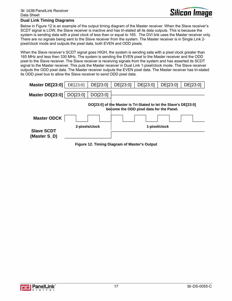
Dual Link Timing Diagrams Below in Figure 12 is an example of the output timing diagram of the Master receiver. When the Slave receiver’s SCDT signal is LOW, the Slave receiver is inactive and has tri-stated all its data outputs. This is because the system is sending data with a pixel clock of less than or equal to 165. The DVI link uses the Master receiver only. There are no signals being sent to the Slave receiver from the system. The Master receiver is in Single Link 2-pixel/clock mode and outputs the pixel data, both EVEN and ODD pixels. When the Slave receiver’s SCDT signal goes HIGH, the system is sending sata with a pixel clock greater than 165 MHz and less then 330 MHz. The system is sending the EVEN pixel to the Master receiver and the ODD pixel to the Slave receiver. The Slave receiver is receiving signals from the system and has asserted its SCDT signal to the Master receiver. This puts the Master receiver in Dual Link 1-pixel/clock mode. The Slave receiver outputs the ODD pixel data. The Master receiver outputs the EVEN pixel data. The Master receiver has tri-stated its ODD pixel bus to allow the Slave receiver to send ODD pixel data.
DE[23:0] DE[23:0]
DO[23:0] DO[23:0]
DE[23:0] DE[23:0] DE[23:0] DE[23:0]
Slave SCDT(Master S_D)
Master ODCK
Master DO[23:0]
Master DE[23:0]
DO[23:0] of the Master is Tri-Stated to let the Slave's DE[23:0]become the ODD pixel data for the Panel.
2-pixels/clock 1-pixel/clock
Figure 12. Timing Diagram of Master's Output
SiI 163B PanelLink Receiver Data Sheet
18 SiI-DS-0055-C
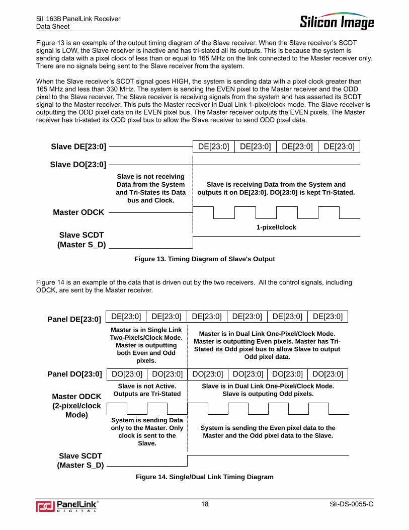
Figure 13 is an example of the output timing diagram of the Slave receiver. When the Slave receiver’s SCDT signal is LOW, the Slave receiver is inactive and has tri-stated all its outputs. This is because the system is sending data with a pixel clock of less than or equal to 165 MHz on the link connected to the Master receiver only. There are no signals being sent to the Slave receiver from the system. When the Slave receiver’s SCDT signal goes HIGH, the system is sending data with a pixel clock greater than 165 MHz and less than 330 MHz. The system is sending the EVEN pixel to the Master receiver and the ODD pixel to the Slave receiver. The Slave receiver is receiving signals from the system and has asserted its SCDT signal to the Master receiver. This puts the Master receiver in Dual Link 1-pixel/clock mode. The Slave receiver is outputting the ODD pixel data on its EVEN pixel bus. The Master receiver outputs the EVEN pixels. The Master receiver has tri-stated its ODD pixel bus to allow the Slave receiver to send ODD pixel data.
DE[23:0] DE[23:0] DE[23:0] DE[23:0]
Slave SCDT(Master S_D)
Master ODCK
Slave DO[23:0]
Slave DE[23:0]
Slave is receiving Data from the System andoutputs it on DE[23:0]. DO[23:0] is kept Tri-Stated.
Slave is not receivingData from the Systemand Tri-States its Data
bus and Clock.
1-pixel/clock
Figure 13. Timing Diagram of Slave's Output
Figure 14 is an example of the data that is driven out by the two receivers. All the control signals, including ODCK, are sent by the Master receiver.
DE[23:0] DE[23:0]
DO[23:0] DO[23:0]
DE[23:0] DE[23:0]
DO[23:0] DO[23:0]
DE[23:0] DE[23:0]
DO[23:0] DO[23:0]
Slave SCDT(Master S_D)
Master ODCK(2-pixel/clock
Mode)
Panel DO[23:0]
Panel DE[23:0]
Slave is not Active.Outputs are Tri-Stated
Master is in Single LinkTwo-Pixels/Clock Mode.
Master is outputtingboth Even and Odd
pixels.
Master is in Dual Link One-Pixel/Clock Mode.Master is outputting Even pixels. Master has Tri-Stated its Odd pixel bus to allow Slave to output
Odd pixel data.
Slave is in Dual Link One-Pixel/Clock Mode.Slave is outputing Odd pixels.
System is sending Dataonly to the Master. Only
clock is sent to theSlave.
System is sending the Even pixel data to theMaster and the Odd pixel data to the Slave.
Figure 14. Single/Dual Link Timing Diagram

SiI 163B PanelLink Receiver Data Sheet
19 SiI-DS-0055-C
Table 4. DVI-D Connector to SiI 163B for Dual Link Application Pin Connection
DVI-D Connector SiI 163B - Master SiI 163B - Slave Pin # Signal Pin # Pin Name Pin # Pin Name
1 TMDS Data2- 81 Rx2- for Master 2 TMDS Data2+ 80 Rx2+ for Master 3 TMDS Data2/4 Shield 4 TMDS Data4- 86 Rx1- for Slave 5 TMDS Data4+ 85 Rx1+ for Slave 6 DDC Clock 7 DDC Data 8 NC 9 TMDS Data1- 86 Rx1- for Master 10 TMDS Data1+ 85 Rx1+ for Master 11 TMDS Data1/3 Shield 12 TMDS Data3- 91 Rx0- for Slave 13 TMDS Data3+ 90 Rx0+ for Slave 14 +5V Power 15 Ground 16 Hot Plug Detect 17 TMDS Data0- 91 Rx0- for Master 18 TMDS Data0+ 90 Rx0+ for Master 19 TMDS Data0/5 Shield 20 TMDS Data5- 81 Rx2- for Slave 21 TMDS Data5+ 80 Rx2+ for Slave 22 TMDS Clock Shield 23 TMDS Clock+ 93 RxC+ for Master 93 RxC+ for Slave 24 TMDS Clock- 94 RxC- for Master 94 RxC- for Slave
Clock Detect Function The SiI 163B includes a new power saving feature: power down with clock detect circuit. The SiI 163B will go into a low power mode when there is no video clock coming from the transmitter. In this mode, the entire chip is powered down except the clock detect circuitry. During this mode, digital I/O are set to a high impedance (tri-state) mode. A weak internal pull-down device brings each output to ground. The device power down and wake-up times are shown in Figure 6 and Figure 7.
OCK_INV# Function
OCK_INV# affects only the phase of the clock output as indicated in Figure 15. OCK_INV# does not change the timing for the internal data latching. This timing is shown in Figure 5.
QE[23:0]
QO[23:0]
ODCK
OCK_INV#
Figure 15. Block Diagram for OCK_INV#

SiI 163B PanelLink Receiver Data Sheet
20 SiI-DS-0055-C
TFT Panel Data Mapping Table 5 summarizes the output data mapping in one pixel per clock mode for the SiI 163B. This output data mapping is dependent upon the PanelLink transmitters having the exact same type of input data mappings.
Table 6 summarizes the output data mapping in two pixel per clock mode. More detailed mapping information is found on the following pages. Refer to application note SiI-AN-0007 for DSTN applications.
Note that the choice of one pixel/clock versus two pixel/clock on the transmitter side has no effect on the choice of one pixel/clock versus two pixel/clock on the receiver side. The data is always sent across the link at the pixel clock rate. Therefore, designers using PanelLink receivers do not need to know how the transmitter has taken in pixel data on the transmitter input pins.
Table 5. One Pixel/Clock Mode Data Mapping
SiI 163B DATA
1-Pixel/Clock Output
18bpp 24bpp
BLUE[7:0] QE[7:2] QE[7:0]
GREEN[7:0] QE[15:10] QE[15:8]
RED[7:0] QE[23:18] QE[23:16]
Table 6. Two Pixel/Clock Mode Data Mapping
SiI 163B DATA
2-Pixel/Clock Output
18bpp 24bpp
BLUE[7:0] – 0 QE[7:2] QE[7:0]
GREEN[7:0] – 0 QE[15:10] QE[15:8]
RED[7:0] – 0 QE[23:18] QE[23:16]
BLUE[7:0] – 1 QO[7:2] QO[7:0]
GREEN[7:0] – 1 QO[15:10] QO[15:8]
RED[7:0] – 1 QO[23:18] QO[23:16]
SiI 163B PanelLink Receiver Data Sheet
21 SiI-DS-0055-C
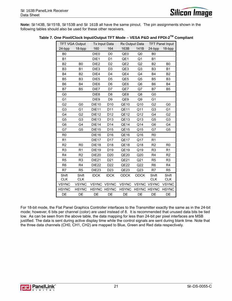
Note: SiI143B, SiI151B, SiI153B and SiI 161B all have the same pinout. The pin assignments shown in the following tables should also be used for these other receivers.
Table 7. One Pixel/Clock Input/Output TFT Mode – VESA P&D and FPDI-2TM Compliant TFT VGA Output Tx Input Data Rx Output Data TFT Panel Input
24-bpp 18-bpp 160 164 163B 141B 24-bpp 18-bpp B0 DIE0 D0 QE0 Q0 B0 B1 DIE1 D1 QE1 Q1 B1 B2 B0 DIE2 D2 QE2 Q2 B2 B0 B3 B1 DIE3 D3 QE3 Q3 B3 B1 B4 B2 DIE4 D4 QE4 Q4 B4 B2 B5 B3 DIE5 D5 QE5 Q5 B5 B3 B6 B4 DIE6 D6 QE6 Q6 B6 B4 B7 B5 DIE7 D7 QE7 Q7 B7 B5 G0 DIE8 D8 QE8 Q8 G0 G1 DIE9 D9 QE9 Q9 G1 G2 G0 DIE10 D10 QE10 Q10 G2 G0 G3 G1 DIE11 D11 QE11 Q11 G3 G1 G4 G2 DIE12 D12 QE12 Q12 G4 G2 G5 G3 DIE13 D13 QE13 Q13 G5 G3 G6 G4 DIE14 D14 QE14 Q14 G6 G4 G7 G5 DIE15 D15 QE15 Q15 G7 G5 R0 DIE16 D16 QE16 Q16 R0 R1 DIE17 D17 QE17 Q17 R1 R2 R0 DIE18 D18 QE18 Q18 R2 R0 R3 R1 DIE19 D19 QE19 Q19 R3 R1 R4 R2 DIE20 D20 QE20 Q20 R4 R2 R5 R3 DIE21 D21 QE21 Q21 R5 R3 R6 R4 DIE22 D22 QE22 Q22 R6 R4 R7 R5 DIE23 D23 QE23 Q23 R7 R5
Shift CLK
Shift CLK
IDCK IDCK ODCK ODCK Shift CLK
Shift CLK
VSYNC VSYNC VSYNC VSYNC VSYNC VSYNC VSYNC VSYNC HSYNC HSYNC HSYNC HSYNC HSYNC HSYNC HSYNC HSYNC
DE DE DE DE DE DE DE DE For 18-bit mode, the Flat Panel Graphics Controller interfaces to the Transmitter exactly the same as in the 24-bit mode; however, 6 bits per channel (color) are used instead of 8. It is recommended that unused data bits be tied low. As can be seen from the above table, the data mapping for less than 24-bit per pixel interfaces are MSB justified. The data is sent during active display time while the control signals are sent during blank time. Note that the three data channels (CH0, CH1, CH2) are mapped to Blue, Green and Red data respectively.
SiI 163B PanelLink Receiver Data Sheet
22 SiI-DS-0055-C
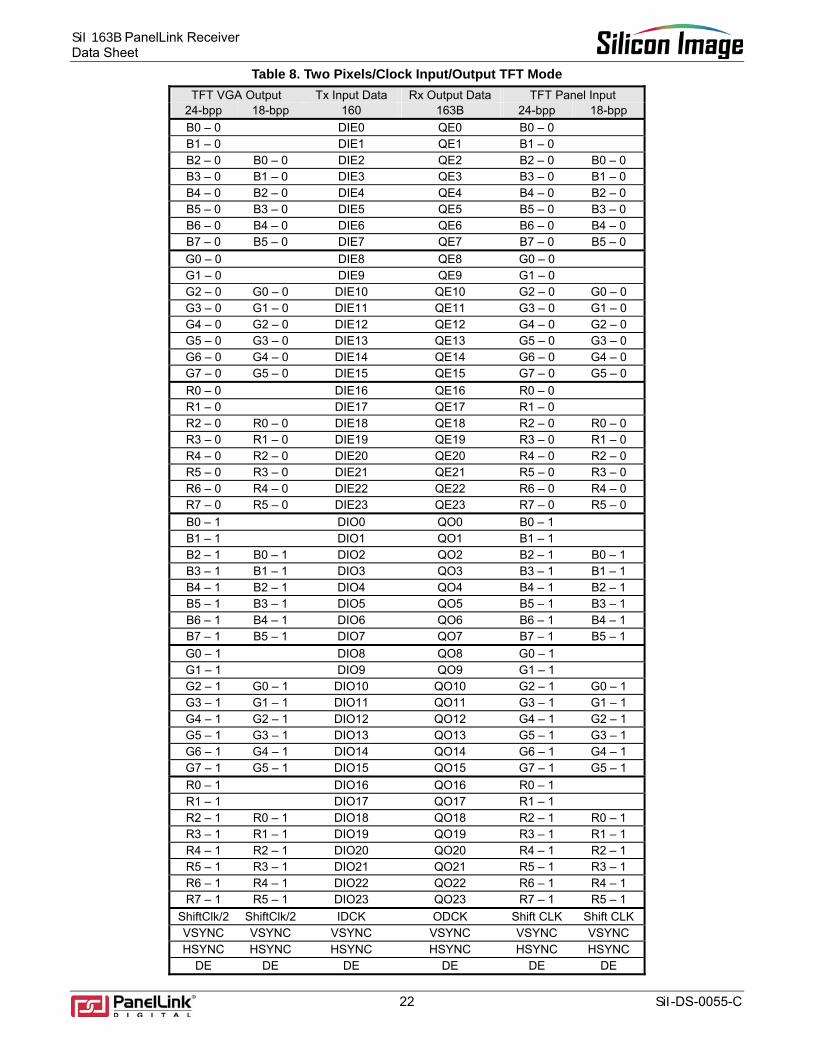
Table 8. Two Pixels/Clock Input/Output TFT Mode TFT VGA Output Tx Input Data Rx Output Data TFT Panel Input
24-bpp 18-bpp 160 163B 24-bpp 18-bpp B0 – 0 DIE0 QE0 B0 – 0 B1 – 0 DIE1 QE1 B1 – 0 B2 – 0 B0 – 0 DIE2 QE2 B2 – 0 B0 – 0 B3 – 0 B1 – 0 DIE3 QE3 B3 – 0 B1 – 0 B4 – 0 B2 – 0 DIE4 QE4 B4 – 0 B2 – 0 B5 – 0 B3 – 0 DIE5 QE5 B5 – 0 B3 – 0 B6 – 0 B4 – 0 DIE6 QE6 B6 – 0 B4 – 0 B7 – 0 B5 – 0 DIE7 QE7 B7 – 0 B5 – 0 G0 – 0 DIE8 QE8 G0 – 0 G1 – 0 DIE9 QE9 G1 – 0 G2 – 0 G0 – 0 DIE10 QE10 G2 – 0 G0 – 0 G3 – 0 G1 – 0 DIE11 QE11 G3 – 0 G1 – 0 G4 – 0 G2 – 0 DIE12 QE12 G4 – 0 G2 – 0 G5 – 0 G3 – 0 DIE13 QE13 G5 – 0 G3 – 0 G6 – 0 G4 – 0 DIE14 QE14 G6 – 0 G4 – 0 G7 – 0 G5 – 0 DIE15 QE15 G7 – 0 G5 – 0 R0 – 0 DIE16 QE16 R0 – 0 R1 – 0 DIE17 QE17 R1 – 0 R2 – 0 R0 – 0 DIE18 QE18 R2 – 0 R0 – 0 R3 – 0 R1 – 0 DIE19 QE19 R3 – 0 R1 – 0 R4 – 0 R2 – 0 DIE20 QE20 R4 – 0 R2 – 0 R5 – 0 R3 – 0 DIE21 QE21 R5 – 0 R3 – 0 R6 – 0 R4 – 0 DIE22 QE22 R6 – 0 R4 – 0 R7 – 0 R5 – 0 DIE23 QE23 R7 – 0 R5 – 0 B0 – 1 DIO0 QO0 B0 – 1 B1 – 1 DIO1 QO1 B1 – 1 B2 – 1 B0 – 1 DIO2 QO2 B2 – 1 B0 – 1 B3 – 1 B1 – 1 DIO3 QO3 B3 – 1 B1 – 1 B4 – 1 B2 – 1 DIO4 QO4 B4 – 1 B2 – 1 B5 – 1 B3 – 1 DIO5 QO5 B5 – 1 B3 – 1 B6 – 1 B4 – 1 DIO6 QO6 B6 – 1 B4 – 1 B7 – 1 B5 – 1 DIO7 QO7 B7 – 1 B5 – 1 G0 – 1 DIO8 QO8 G0 – 1 G1 – 1 DIO9 QO9 G1 – 1 G2 – 1 G0 – 1 DIO10 QO10 G2 – 1 G0 – 1 G3 – 1 G1 – 1 DIO11 QO11 G3 – 1 G1 – 1 G4 – 1 G2 – 1 DIO12 QO12 G4 – 1 G2 – 1 G5 – 1 G3 – 1 DIO13 QO13 G5 – 1 G3 – 1 G6 – 1 G4 – 1 DIO14 QO14 G6 – 1 G4 – 1 G7 – 1 G5 – 1 DIO15 QO15 G7 – 1 G5 – 1 R0 – 1 DIO16 QO16 R0 – 1 R1 – 1 DIO17 QO17 R1 – 1 R2 – 1 R0 – 1 DIO18 QO18 R2 – 1 R0 – 1 R3 – 1 R1 – 1 DIO19 QO19 R3 – 1 R1 – 1 R4 – 1 R2 – 1 DIO20 QO20 R4 – 1 R2 – 1 R5 – 1 R3 – 1 DIO21 QO21 R5 – 1 R3 – 1 R6 – 1 R4 – 1 DIO22 QO22 R6 – 1 R4 – 1 R7 – 1 R5 – 1 DIO23 QO23 R7 – 1 R5 – 1
ShiftClk/2 ShiftClk/2 IDCK ODCK Shift CLK Shift CLK VSYNC VSYNC VSYNC VSYNC VSYNC VSYNC HSYNC HSYNC HSYNC HSYNC HSYNC HSYNC
DE DE DE DE DE DE

SiI 163B PanelLink Receiver Data Sheet
23 SiI-DS-0055-C
Table 9. 24-bit One Pixel/Clock Input with 24-bit Two Pixels/Clock Output TFT Mode TFT VGA Output Tx Input Data Rx Output Data TFT Panel Input
24-bpp 160 164 163B 24-bpp B0 DIE0 D0 QE0 B0 – 0 B1 DIE1 D1 QE1 B1 – 0 B2 DIE2 D2 QE2 B2 – 0 B3 DIE3 D3 QE3 B3 – 0 B4 DIE4 D4 QE4 B4 – 0 B5 DIE5 D5 QE5 B5 – 0 B6 DIE6 D6 QE6 B6 – 0 B7 DIE7 D7 QE7 B7 – 0 G0 DIE8 D8 QE8 G0 – 0 G1 DIE9 D9 QE9 G1 – 0 G2 DIE10 D10 QE10 G2 – 0 G3 DIE11 D11 QE11 G3 – 0 G4 DIE12 D12 QE12 G4 – 0 G5 DIE13 D13 QE13 G5 – 0 G6 DIE14 D14 QE14 G6 – 0 G7 DIE15 D15 QE15 G7 – 0 R0 DIE16 D16 QE16 R0 – 0 R1 DIE17 D17 QE17 R1 – 0 R2 DIE18 D18 QE18 R2 – 0 R3 DIE19 D19 QE19 R3 – 0 R4 DIE20 D20 QE20 R4 – 0 R5 DIE21 D21 QE21 R5 – 0 R6 DIE22 D22 QE22 R6 – 0 R7 DIE23 D23 QE23 R7 – 0
QO0 B0 – 1 QO1 B1 – 1 QO2 B2 – 1 QO3 B3 – 1 QO4 B4 – 1 QO5 B5 – 1 QO6 B6 – 1 QO7 B7 – 1 QO8 G0 – 1 QO9 G1 – 1 QO10 G2 – 1 QO11 G3 – 1 QO12 G4 – 1 QO13 G5 – 1 QO14 G6 – 1 QO15 G7 – 1 QO16 R0 – 1 QO17 R1 – 1 QO18 R2 – 1 QO19 R3 – 1 QO20 R4 – 1 QO21 R5 – 1 QO22 R6 – 1 QO23 R7 – 1
Shift CLK IDCK IDCK ODCK Shift CLK/2 VSYNC VSYNC VSYNC VSYNC VSYNC HSYNC HSYNC HSYNC HSYNC HSYNC
DE DE DE DE DE

SiI 163B PanelLink Receiver Data Sheet
24 SiI-DS-0055-C
Table 10. 18-bit One Pixel/Clock Input with 18-bit Two Pixels/Clock Output TFT Mode TFT VGA Output Tx Input Data Tx Output Data TFT Panel Input
18-bpp 160 164 163B 141B 18-bpp DIE0 D0 QE0 DIE1 D1 QE1
B0 DIE2 D2 QE2 Q0 B0 – 0 B1 DIE3 D3 QE3 Q1 B1 – 0 B2 DIE4 D4 QE4 Q2 B2 – 0 B3 DIE5 D5 QE5 Q3 B3 – 0 B4 DIE6 D6 QE6 Q4 B4 – 0 B5 DIE7 D7 QE7 Q5 B5 – 0
DIE8 D8 QE8 DIE9 D9 QE9
G0 DIE10 D10 QE10 Q6 G0 – 0 G1 DIE11 D11 QE11 Q7 G1 – 0 G2 DIE12 D12 QE12 Q8 G2 – 0 G3 DIE13 D13 QE13 Q9 G3 – 0 G4 DIE14 D14 QE14 Q10 G4 – 0 G5 DIE15 D15 QE15 Q11 G5 – 0
DIE16 D16 QE16 DIE17 D17 QE17
R0 DIE18 D18 QE18 Q12 R0 – 0 R1 DIE19 D19 QE19 Q13 R1 – 0 R2 DIE20 D20 QE20 Q14 R2 – 0 R3 DIE21 D21 QE21 Q15 R3 – 0 R4 DIE22 D22 QE22 Q16 R4 – 0 R5 DIE23 D23 QE23 Q17 R5 – 0
QO0 QO1 QO2 Q18 B0 – 1 QO3 Q19 B1 – 1 QO4 Q20 B2 – 1 QO5 Q21 B3 – 1 QO6 Q22 B4 – 1 QO7 Q23 B5 – 1 QO8 QO9 QO10 Q24 G0 – 1 QO11 Q25 G1 – 1 QO12 Q26 G2 – 1 QO13 Q27 G3 – 1 QO14 Q28 G4 – 1 QO15 Q29 G5 – 1 QO16 QO17 QO18 Q30 R0 – 1 QO19 Q31 R1 – 1 QO20 Q32 R2 – 1 QO21 Q33 R3 – 1 QO22 Q34 R4 – 1 QO23 Q35 R5 – 1
Shift CLK IDCK IDCK ODCK Shift CLK/2 Shift CLK/2 VSYNC VSYNC VSYNC VSYNC VSYNC VSYNC HSYNC HSYNC HSYNC HSYNC HSYNC HSYNC
DE DE DE DE DE DE

SiI 163B PanelLink Receiver Data Sheet
25 SiI-DS-0055-C
Table 11. Two Pixels/Clock Input with One Pixel/Clock Output TFT Mode TFT VGA Output Tx Input Data Rx Output Data TFT Panel Input
24-bpp 18-bpp 160 163B 141B 24-bpp 18-bpp B0 – 0 DIE0 QE0 Q0 B0 B1 – 0 DIE1 QE1 Q1 B1 B2 – 0 B0 – 0 DIE2 QE2 Q2 B2 B0 B3 – 0 B1 – 0 DIE3 QE3 Q3 B3 B1 B4 – 0 B2 – 0 DIE4 QE4 Q4 B4 B2 B5 – 0 B3 – 0 DIE5 QE5 Q5 B5 B3 B6 – 0 B4 – 0 DIE6 QE6 Q6 B6 B4 B7 – 0 B5 – 0 DIE7 QE7 Q7 B7 B5 G0 – 0 DIE8 QE8 Q8 G0 G1 – 0 DIE9 QE9 Q9 G1 G2 – 0 G0 – 0 DIE10 QE10 Q10 G2 G0 G3 – 0 G1 – 0 DIE11 QE11 Q11 G3 G1 G4 – 0 G2 – 0 DIE12 QE12 Q12 G4 G2 G5 – 0 G3 – 0 DIE13 QE13 Q13 G5 G3 G6 – 0 G4 – 0 DIE14 QE14 Q14 G6 G4 G7 – 0 G5 – 0 DIE15 QE15 Q15 G7 G5 R0 – 0 DIE16 QE16 Q16 R0 R1 – 0 DIE17 QE17 Q17 R1 R2 – 0 R0 – 0 DIE18 QE18 Q18 R2 R0 R3 – 0 R1 – 0 DIE19 QE19 Q19 R3 R1 R4 – 0 R2 – 0 DIE20 QE20 Q20 R4 R2 R5 – 0 R3 – 0 DIE21 QE21 Q21 R5 R3 R6 – 0 R4 – 0 DIE22 QE22 Q22 R6 R4 R7 – 0 R5 – 0 DIE23 QE23 Q23 R7 R5 B0 – 1 DIO0 B1 – 1 DIO1 B2 – 1 B0 – 1 DIO2 B3 – 1 B1 – 1 DIO3 B4 – 1 B2 – 1 DIO4 B5 – 1 B3 – 1 DIO5 B6 – 1 B4 – 1 DIO6 B7 – 1 B5 – 1 DIO7 G0 – 1 DIO8 G1 – 1 DIO9 G2 – 1 G0 – 1 DIO10 G3 – 1 G1 – 1 DIO11 G4 – 1 G2 – 1 DIO12 G5 – 1 G3 – 1 DIO13 G6 – 1 G4 – 1 DIO14 G7 – 1 G5 – 1 DIO15 R0 – 1 DIO16 R1 – 1 DIO17 R2 – 1 R0 – 1 DIO18 R3 – 1 R1 – 1 DIO19 R4 – 1 R2 – 1 DIO20 R5 – 1 R3 – 1 DIO21 R6 – 1 R4 – 1 DIO22 R7 – 1 R5 – 1 DIO23
ShiftClk/2 ShiftClk/2 IDCK ODCK ODCK ShiftClk ShiftClk VSYNC VSYNC VSYNC VSYNC VSYNC VSYNC VSYNC HSYNC HSYNC HSYNC HSYNC HSYNC HSYNC HSYNC
DE DE DE DE DE DE DE
SiI 163B PanelLink Receiver Data Sheet
26 SiI-DS-0055-C
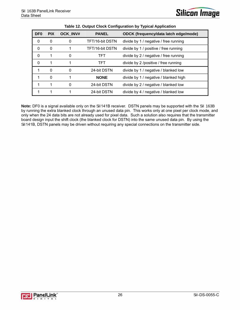
Table 12. Output Clock Configuration by Typical Application
DF0 PIX OCK_INV# PANEL ODCK (frequency/data latch edge/mode)
0 0 0 TFT/16-bit DSTN divide by 1 / negative / free running
0 0 1 TFT/16-bit DSTN divide by 1 / positive / free running
0 1 0 TFT divide by 2 / negative / free running
0 1 1 TFT divide by 2 /positive / free running
1 0 0 24-bit DSTN divide by 1 / negative / blanked low
1 0 1 NONE divide by 1 / negative / blanked high
1 1 0 24-bit DSTN divide by 2 / negative / blanked low
1 1 1 24-bit DSTN divide by 4 / negative / blanked low
Note: DF0 is a signal available only on the SiI141B receiver. DSTN panels may be supported with the SiI 163B by running the extra blanked clock through an unused data pin. This works only at one pixel per clock mode, and only when the 24 data bits are not already used for pixel data. Such a solution also requires that the transmitter board design input the shift clock (the blanked clock for DSTN) into the same unused data pin. By using the SiI141B, DSTN panels may be driven without requiring any special connections on the transmitter side.
SiI 163B PanelLink Receiver Data Sheet
27 SiI-DS-0055-C
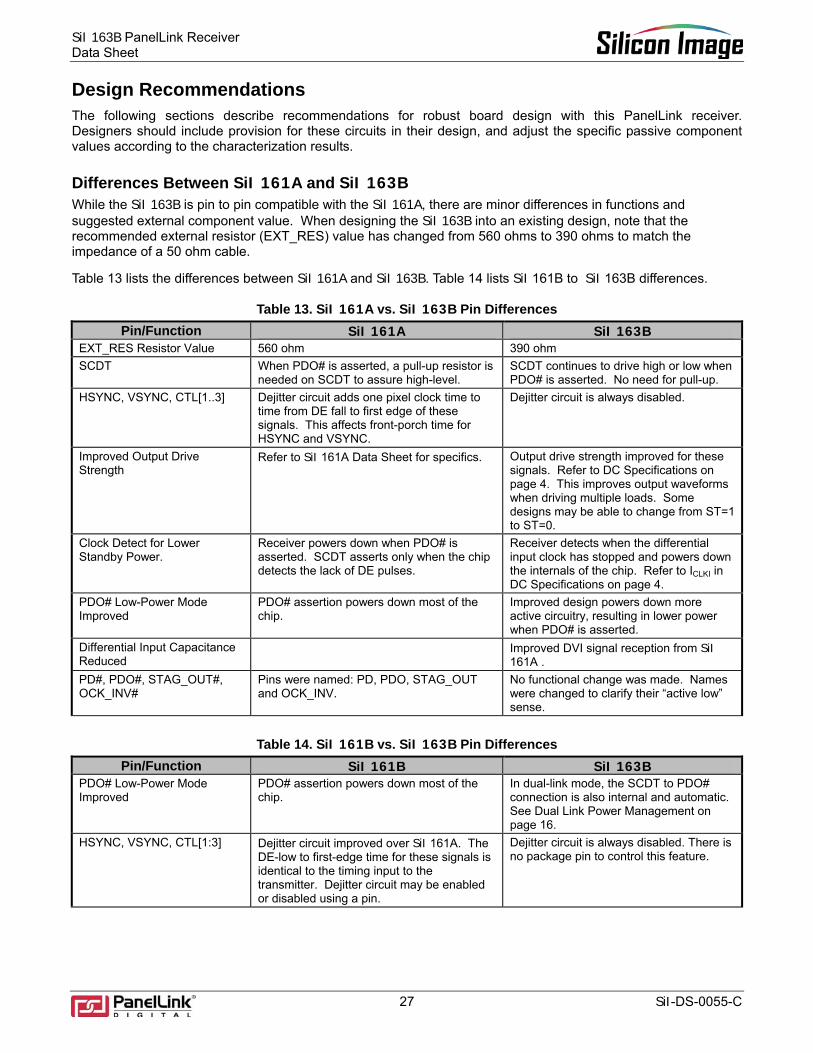
Design Recommendations The following sections describe recommendations for robust board design with this PanelLink receiver. Designers should include provision for these circuits in their design, and adjust the specific passive component values according to the characterization results.
Differences Between SiI 161A and SiI 163B While the SiI 163B is pin to pin compatible with the SiI 161A, there are minor differences in functions and suggested external component value. When designing the SiI 163B into an existing design, note that the recommended external resistor (EXT_RES) value has changed from 560 ohms to 390 ohms to match the impedance of a 50 ohm cable.
Table 13 lists the differences between SiI 161A and SiI 163B. Table 14 lists SiI 161B to SiI 163B differences.
Table 13. SiI 161A vs. SiI 163B Pin Differences Pin/Function SiI 161A SiI 163B
EXT_RES Resistor Value 560 ohm 390 ohm SCDT When PDO# is asserted, a pull-up resistor is
needed on SCDT to assure high-level. SCDT continues to drive high or low when PDO# is asserted. No need for pull-up.
HSYNC, VSYNC, CTL[1..3] Dejitter circuit adds one pixel clock time to time from DE fall to first edge of these signals. This affects front-porch time for HSYNC and VSYNC.
Dejitter circuit is always disabled.
Improved Output Drive Strength
Refer to SiI 161A Data Sheet for specifics. Output drive strength improved for these signals. Refer to DC Specifications on page 4. This improves output waveforms when driving multiple loads. Some designs may be able to change from ST=1 to ST=0.
Clock Detect for Lower Standby Power.
Receiver powers down when PDO# is asserted. SCDT asserts only when the chip detects the lack of DE pulses.
Receiver detects when the differential input clock has stopped and powers down the internals of the chip. Refer to ICLKI in DC Specifications on page 4.
PDO# Low-Power Mode Improved
PDO# assertion powers down most of the chip.
Improved design powers down more active circuitry, resulting in lower power when PDO# is asserted.
Differential Input Capacitance Reduced
Improved DVI signal reception from SiI 161A .
PD#, PDO#, STAG_OUT#, OCK_INV#
Pins were named: PD, PDO, STAG_OUT and OCK_INV.
No functional change was made. Names were changed to clarify their “active low” sense.
Table 14. SiI 161B vs. SiI 163B Pin Differences
Pin/Function SiI 161B SiI 163B PDO# Low-Power Mode Improved
PDO# assertion powers down most of the chip.
In dual-link mode, the SCDT to PDO# connection is also internal and automatic. See Dual Link Power Management on page 16.
HSYNC, VSYNC, CTL[1:3] Dejitter circuit improved over SiI 161A. The DE-low to first-edge time for these signals is identical to the timing input to the transmitter. Dejitter circuit may be enabled or disabled using a pin.
Dejitter circuit is always disabled. There is no package pin to control this feature.

SiI 163B PanelLink Receiver Data Sheet
28 SiI-DS-0055-C
Voltage Ripple Regulation The power supply to VCC pins is very important to the proper operation of the receiver chips. Two examples of regulators are shown in Figure 16 and Figure 17.
1K ohms1%
3K ohms1%
Vin=5V Vout=3.3V
TL431
Figure 16. Voltage Regulation using TL431
Decoupling and bypass capacitors are also involved with power supply connections, as described in detail in Figure 19.
240 ohms
390 ohms
Vin=5V
Vout=3.3V
ADJ
Vin Vout
LM317EMP
Figure 17. Voltage Regulation using LM317

SiI 163B PanelLink Receiver Data Sheet
29 SiI-DS-0055-C
Decoupling Capacitors Designers should include decoupling and bypass capacitors at each power pin in the layout. These are shown schematically in Figure 19. Place these components as closely as possible to the PanelLink device pins, and avoid routing through vias if possible, as shown in Figure 18, which is representative of the various types of power pins on the receiver.
L1 C1
VCC
Ferrite
Preferable
Via to GND
VCC
GND
C2
C3
Figure 18. Decoupling and Bypass Capacitor Placement
VCCPIN
C1 C2
L1
C3
VCC
Figure 19. Decoupling and Bypass Schematic
Table 15. Recommended Components
C1 C2 C3 L1
100 – 300 pF 2.2 – 10 uF 10 uF 200+ ohms
The values shown in Table 15 are recommendations that should be adjusted according to the noise characteristics of the specific board-level design. Pins in one group (such as OVCC) may share L1 and C3, each pin having C1 placed as closely to the pin as possible.
SiI 163B PanelLink Receiver Data Sheet
30 SiI-DS-0055-C
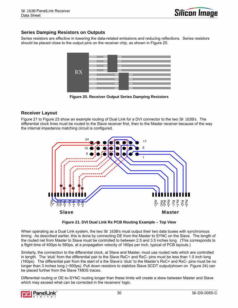
Series Damping Resistors on Outputs Series resistors are effective in lowering the data-related emissions and reducing reflections. Series resistors should be placed close to the output pins on the receiver chip, as shown in Figure 20.
RX
Figure 20. Receiver Output Series Damping Resistors
Receiver Layout Figure 21 to Figure 23 show an example routing of Dual Link for a DVI connector to the two SiI 163B’s. The differential clock lines must be routed to the Slave receiver first, then to the Master receiver because of the way the internal impedance matching circuit is configured.
Rx2+
Rx2-
Rx1+
Rx1-
Rx0+
Rx0-
RxC+
RxC
-
Rx2+
Rx2-
Rx1+
Rx1-
Rx0+
Rx0-
RxC+
RxC
-
18
916
1724
Slave Master
Figure 21. DVI Dual Link Rx PCB Routing Example – Top View When operating as a Dual Link system, the two SiI 163B’s must output their two data buses with synchronous timing. As described earlier, this is done by connecting DE from the Master to SYNC on the Slave. The length of the routed net from Master to Slave must be controlled to between 2.5 and 3.5 inches long. (This corresponds to a flight time of 400ps to 560ps, at a propagation velocity of 160ps per inch, typical of PCB layouts.)
Similarly, the connection to the differential clock, at Slave and Master, must use routed nets which are controlled in length. The ‘stub’ from the differential pair to the Slave RxC+ and RxC- pins must be less than 1.0 inch long (160ps). The differential pair from the start of a the Slave’s ‘stub’ to the Master’s RxC+ and RxC- pins must be no longer than 3 inches long (~500ps). Pull down resistors to stabilize Slave SCDT output(shown on Figure 24) can be placed further from the Slave TMDS traces.
Differential routing or DE-to-SYNC routing longer than these limits will create a skew between Master and Slave which may exceed what can be corrected in the receivers’ logic.

SiI 163B PanelLink Receiver Data Sheet
31 SiI-DS-0055-C
Rx2+
Rx2-
Rx1+
Rx1-
Rx0+
Rx0-
RxC+
RxC
-
Rx2+
Rx2-
Rx1+
Rx1-
Rx0+
Rx0-
RxC+
RxC
-
18
916
1724
Slave Master
Figure 22. DVI Dual Link Rx PCB Routing Example – Top Signals Top View
Rx2+
Rx2-
Rx1+
Rx1-
Rx0+
Rx0-
RxC+
RxC
-
Rx2+
Rx2-
Rx1+
Rx1-
Rx0+
Rx0-
RxC+
RxC
-
18
916
1724
Slave Master
Figure 23. DVI Dual Link Rx PCB Routing Example - Bottom Signals Top View
The receiver chip should be placed as closely as possible to the input connector which carries the TMDS signals. For a system using the industry-standard DVI connector (see http://www.ddwg.org), the differential lines should be routed as directly as possible from connector to receiver. PanelLink devices are tolerant of skews between differential pairs, so spiral skew compensation for path length differences is not required. Each differential pair should be routed together, minimizing the number of vias through which the signal lines are routed.
As defined in the DVI 1.0 Specification, the impedance of the traces between the connector and the receiver should be 100 ohms differentially, and close to 50 ohms single-ended. The 100 ohm requirement is to best match the differential impedance of the cable and connectors, to prevent reflections. The common mode currents are very small on the TMDS interface, so differential impedance is more important than single-ended.
SiI 163B PanelLink Receiver Data Sheet
32 SiI-DS-0055-C
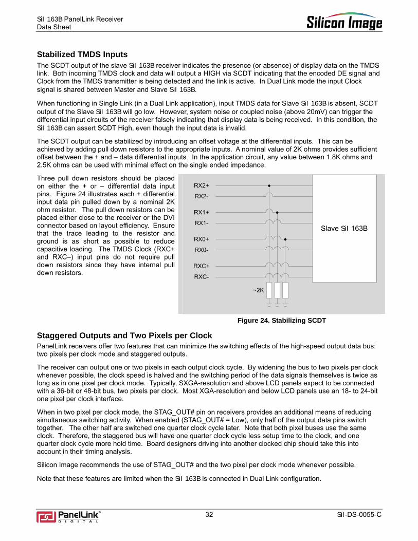
Stabilized TMDS Inputs The SCDT output of the slave SiI 163B receiver indicates the presence (or absence) of display data on the TMDS link. Both incoming TMDS clock and data will output a HIGH via SCDT indicating that the encoded DE signal and Clock from the TMDS transmitter is being detected and the link is active. In Dual Link mode the input Clock signal is shared between Master and Slave SiI 163B.
When functioning in Single Link (in a Dual Link application), input TMDS data for Slave SiI 163B is absent, SCDT output of the Slave SiI 163B will go low. However, system noise or coupled noise (above 20mV) can trigger the differential input circuits of the receiver falsely indicating that display data is being received. In this condition, the SiI 163B can assert SCDT High, even though the input data is invalid.
The SCDT output can be stabilized by introducing an offset voltage at the differential inputs. This can be achieved by adding pull down resistors to the appropriate inputs. A nominal value of 2K ohms provides sufficient offset between the + and – data differential inputs. In the application circuit, any value between 1.8K ohms and 2.5K ohms can be used with minimal effect on the single ended impedance.
Slave SiI 163B
RX2+
RX2-
RX1+
RX1-
RX0+
RX0-
RXC+
RXC-
~2K
Three pull down resistors should be placed on either the + or – differential data input pins. Figure 24 illustrates each + differential input data pin pulled down by a nominal 2K ohm resistor. The pull down resistors can be placed either close to the receiver or the DVI connector based on layout efficiency. Ensure that the trace leading to the resistor and ground is as short as possible to reduce capacitive loading. The TMDS Clock (RXC+ and RXC–) input pins do not require pull down resistors since they have internal pull down resistors.
Figure 24. Stabilizing SCDT
Staggered Outputs and Two Pixels per Clock PanelLink receivers offer two features that can minimize the switching effects of the high-speed output data bus: two pixels per clock mode and staggered outputs.
The receiver can output one or two pixels in each output clock cycle. By widening the bus to two pixels per clock whenever possible, the clock speed is halved and the switching period of the data signals themselves is twice as long as in one pixel per clock mode. Typically, SXGA-resolution and above LCD panels expect to be connected with a 36-bit or 48-bit bus, two pixels per clock. Most XGA-resolution and below LCD panels use an 18- to 24-bit one pixel per clock interface.
When in two pixel per clock mode, the STAG_OUT# pin on receivers provides an additional means of reducing simultaneous switching activity. When enabled (STAG_OUT# = Low), only half of the output data pins switch together. The other half are switched one quarter clock cycle later. Note that both pixel buses use the same clock. Therefore, the staggered bus will have one quarter clock cycle less setup time to the clock, and one quarter clock cycle more hold time. Board designers driving into another clocked chip should take this into account in their timing analysis.
Silicon Image recommends the use of STAG_OUT# and the two pixel per clock mode whenever possible.
Note that these features are limited when the SiI 163B is connected in Dual Link configuration.
SiI 163B PanelLink Receiver Data Sheet
33 SiI-DS-0055-C
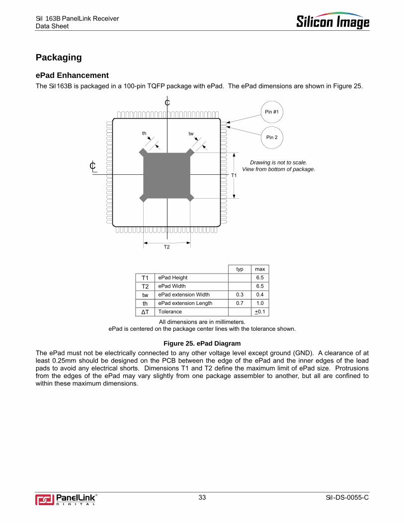
Packaging
ePad Enhancement The SiI163B is packaged in a 100-pin TQFP package with ePad. The ePad dimensions are shown in Figure 25.
C
T2
T1
C
Drawing is not to scale.View from bottom of package.
Pin #1
Pin 2twth
typ max
T1 ePad Height 6.5
T2 ePad Width 6.5
tw ePad extension Width 0.3 0.4
th ePad extension Length 0.7 1.0
∆T Tolerance +0.1
All dimensions are in millimeters. ePad is centered on the package center lines with the tolerance shown.
Figure 25. ePad Diagram The ePad must not be electrically connected to any other voltage level except ground (GND). A clearance of at least 0.25mm should be designed on the PCB between the edge of the ePad and the inner edges of the lead pads to avoid any electrical shorts. Dimensions T1 and T2 define the maximum limit of ePad size. Protrusions from the edges of the ePad may vary slightly from one package assembler to another, but all are confined to within these maximum dimensions.
SiI 163B PanelLink Receiver Data Sheet
34 SiI-DS-0055-C
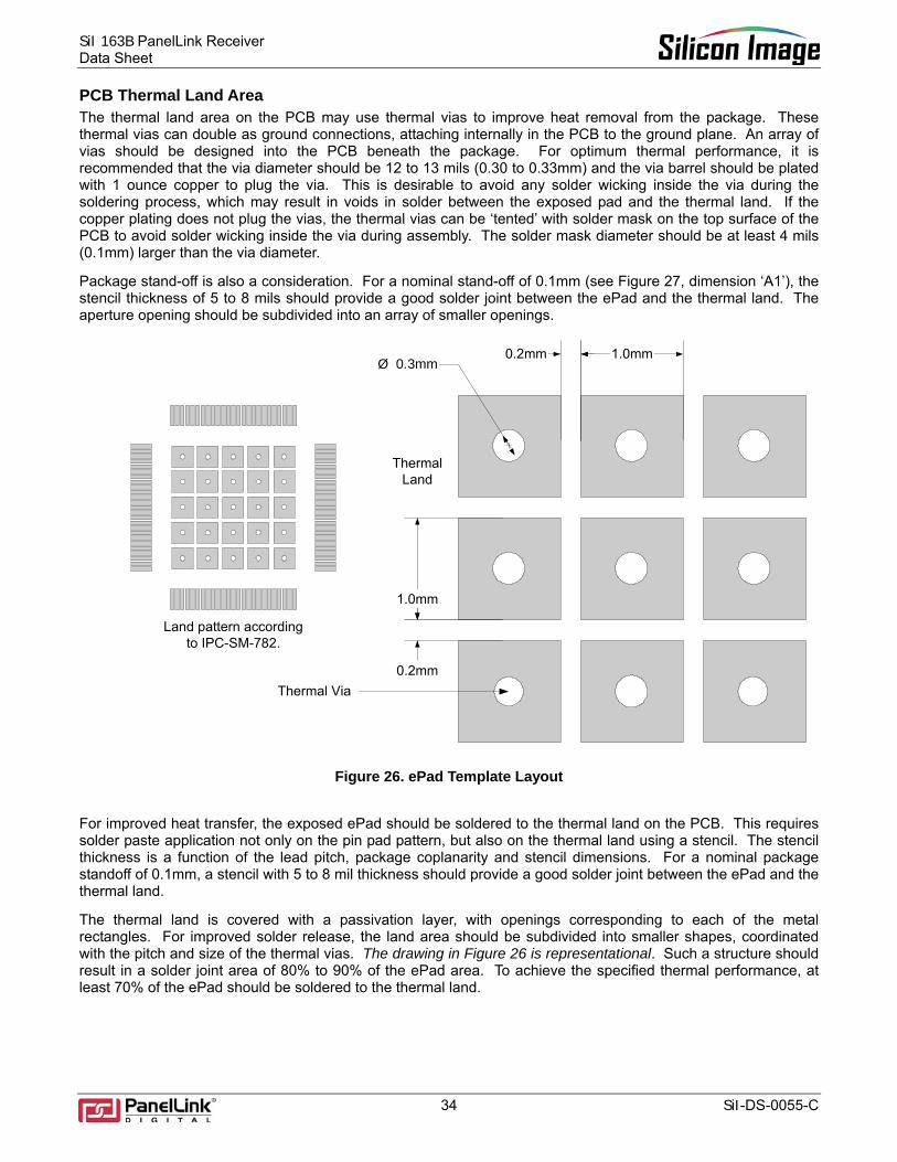
PCB Thermal Land Area The thermal land area on the PCB may use thermal vias to improve heat removal from the package. These thermal vias can double as ground connections, attaching internally in the PCB to the ground plane. An array of vias should be designed into the PCB beneath the package. For optimum thermal performance, it is recommended that the via diameter should be 12 to 13 mils (0.30 to 0.33mm) and the via barrel should be plated with 1 ounce copper to plug the via. This is desirable to avoid any solder wicking inside the via during the soldering process, which may result in voids in solder between the exposed pad and the thermal land. If the copper plating does not plug the vias, the thermal vias can be ‘tented’ with solder mask on the top surface of the PCB to avoid solder wicking inside the via during assembly. The solder mask diameter should be at least 4 mils (0.1mm) larger than the via diameter.
Package stand-off is also a consideration. For a nominal stand-off of 0.1mm (see Figure 27, dimension ‘A1’), the stencil thickness of 5 to 8 mils should provide a good solder joint between the ePad and the thermal land. The aperture opening should be subdivided into an array of smaller openings.
Thermal Via
1.0mm0.2mm
0.2mm
1.0mm
Ø 0.3mm
ThermalLand
Land pattern accordingto IPC-SM-782.
Figure 26. ePad Template Layout
For improved heat transfer, the exposed ePad should be soldered to the thermal land on the PCB. This requires solder paste application not only on the pin pad pattern, but also on the thermal land using a stencil. The stencil thickness is a function of the lead pitch, package coplanarity and stencil dimensions. For a nominal package standoff of 0.1mm, a stencil with 5 to 8 mil thickness should provide a good solder joint between the ePad and the thermal land.
The thermal land is covered with a passivation layer, with openings corresponding to each of the metal rectangles. For improved solder release, the land area should be subdivided into smaller shapes, coordinated with the pitch and size of the thermal vias. The drawing in Figure 26 is representational. Such a structure should result in a solder joint area of 80% to 90% of the ePad area. To achieve the specified thermal performance, at least 70% of the ePad should be soldered to the thermal land.

SiI 163B PanelLink Receiver Data Sheet
35 SiI-DS-0055-C
100-pin TQFP Package Dimensions and Marking Specification
E1 F1
D1
G1
A2
A1
L1
DetailA
DetailB
Drawing is notto scale.
Pin count isrepresentative.
Refer toproduct
specifications.
Cross-sectional representation to showpackage thickness.
SiIxxxxrpppcccLNNNNN.NLLLYYWWX.XX
Device #Lot #
Date CodeRev. Code
e/2
b
Detail A Detail B
0.08 R min
L0.20 min
b
0.08/0.20 R
L1
e
lead cross-section
JEDEC Package Code MS026AED-HD
typ max
A Thickness 1.20
A1 Stand-off 0.15
A2 Body Thickness 1.00 1.05
D1 Body Size 14.00 14.00
E1 Body Size 14.00 14.00
F1 Footprint 16.00 16.00
G1 Footprint 16.00 16.00
Lead Count 100 —
L1 Lead Length 1.00 —
L Lead Foot 0.60 0.75
b Lead Width 0.20 0.27
e Lead Pitch 0.50 —
Dimensions in millimeters. Overall thickness A=A1+A2.
SiIxxxxrppppcccProduct
Designation
Revision
PackageType
PinCount
Universal Package: SiI163BCTG100
Legend Description LNNNNN.NLLL
Lot Number
YY Year of Mfr WW Week of Mfr Rev Code X.XX
Figure 27. Package Dimensions and Marking Specification
Marking Specification Marking drawing is not to scale. Pin counts are representative and may not match the pin count of this product.
Ordering Information Production Part Number: SiI163BCTG100

SiI 163B PanelLink Receiver Data Sheet
36 SiI-DS-0055-C
Summary of Changes The following table lists the major changes to this document up to the present revision.
Revision Date Pages Changes A 03/2002 — Original release. B 08/2004 3, 32, 33-34 Added ePad description. Slave SCDT Stablilization guideline. C 07/2005 33 Fixed ePad dimensions. Part ordering number updated
© 2001-2005 Silicon Image. Inc.
Silicon Image, Inc. Tel: (408) 616-4000 1060 E. Arques Avenue Sunnyvale, CA 94085 USA
Fax: (408) 830-9530 E-mail: [email protected] Web: www.siliconimage.com