iip3 digital current with instantaneous frequency output ... · three phase bidirectional energy...
TRANSCRIPT
Three Phase Bidirectional Energy Metering IC with Instantaneous Frequency Output
SPEC-3093 (REV. 2) 1/15 29-09-2017
SA4305A
FEATURES Meets the IEC62053, CBIP-88 and IS137799-1999
specification requirements for Class 1 AC static watt-
hour meters for active energy
Pulse output supplies instantaneous active power
information
Bidirectional three phase power and energy
measurement
Precision on-chip oscillator (70ppm/°C drift)
Precision on-chip voltage reference (10ppm/°C drift)
Integrated anti-creep function per channel
Low power consumption (<40mW typical)
Measures AC inputs only
Functionally compatible with SA2005F
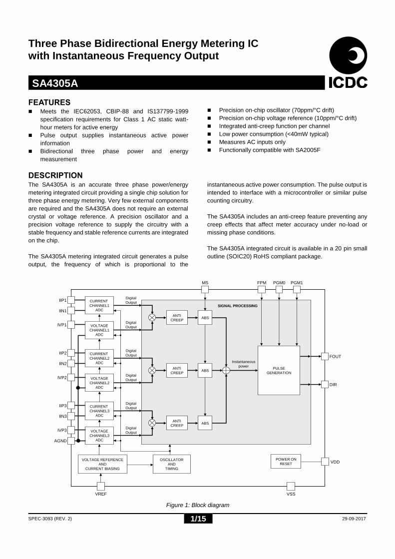
DESCRIPTION The SA4305A is an accurate three phase power/energy
metering integrated circuit providing a single chip solution for
three phase energy metering. Very few external components
are required and the SA4305A does not require an external
crystal or voltage reference. A precision oscillator and a
precision voltage reference to supply the circuitry with a
stable frequency and stable reference currents are integrated
on the chip.
The SA4305A metering integrated circuit generates a pulse
output, the frequency of which is proportional to the
instantaneous active power consumption. The pulse output is
intended to interface with a microcontroller or similar pulse
counting circuitry.
The SA4305A includes an anti-creep feature preventing any
creep effects that affect meter accuracy under no-load or
missing phase conditions.
The SA4305A integrated circuit is available in a 20 pin small
outline (SOIC20) RoHS compliant package.
Figure 1: Block diagram
VREF VSS
OSCILLATOR
AND
TIMING
VOLTAGE REFERENCE
AND
CURRENT BIASING
VOLTAGE
CHANNEL1
ADC
CURRENT
CHANNEL1
ADC
IIP1
POWER ON
RESET
Digital
Output
Instantaneous
power
SIGNAL PROCESSING
FOUT
PULSE
GENERATION
VDD
IIN1
IVP1
AGND
VOLTAGE
CHANNEL2
ADC
CURRENT
CHANNEL2
ADC
IIP2
IIN2
IVP2
VOLTAGE
CHANNEL3
ADC
CURRENT
CHANNEL3
ADC
IIP3
IIN3
IVP3
Digital
Output
Digital
Output
Digital
Output
Digital
Output
Digital
Output
DIR
PGM0 PGM1
ANTI
CREEP
ANTI
CREEP
ANTI
CREEP
FPM
ABS
ABS
ABS
MS

SPEC-3093 (REV. 2) 2/15 29-09-2017
SA4305A
ELECTRICAL CHARACTERISTICS (VDD - VSS = 5V ± 10%, over the temperature range -40°C to +85°C, unless otherwise specified. Refer to Figure 2 “Test circuit for
electrical characteristics”.)
Parameter Symbol Min Typ Max Unit Condition
General
Supply Voltage: Positive
VDD 2.25 2.5 2.75 V With respect to AGND
Supply Voltage: Negative
VSS -2.75 -2.5 -2.25 V With respect to AGND
Supply Current: Positive
IDD 7.5 10.5 mA
Supply Current: Negative
ISS -7.5 -10.5 mA
Analog Inputs
Current Sensor Inputs (Differential)
Input Current Range IRIIP1, IRIIP2, IRIIP3, IRIIN1, IRIIN2, IRIIN3
-25 25 µA Peak value
Offset Voltage VOIIP1, VOIIP2, VOIIP3, VOIIN1, VOIIN2, VOIIN3
-4 4 mV With R = 4.7k connected to AGND
Voltage Sensor Inputs (Asymmetrical)
Input Current Range IRIVP1, IRIVP2, IRIVP3 -25 25 μA Peak value
Offset Voltage VOIVP1, VOIVP2, VOIVP3 -4 4 mV With R = 4.7k connected to AGND
Digital Inputs
PGM0, PGM1, FPM, MS
Input High Voltage
Input Low Voltage
VIH
VIL
VDD-1
VSS+1
V
V
FPM, MS Pull-down
current IPD 40 200 µA
Digital Outputs
FOUT Output Frequency FMAX 1.04 1.16 1.27 kHz
At rated input conditions:
14µARMS on voltage
channels, 16µARMS on
current channels,
MODE 3
FOUT, DIR
Output High Voltage
Output Low Voltage
VOH
VOL
VDD-1
VSS+1
V
V
ISOURCE = 5mA
ISINK = 5mA
During manufacturing, testing and shipment we take great care to protect our products against potential external environmental damage such as Electrostatic Discharge (ESD). Although our products have ESD protection circuitry, permanent damage may occur on products subjected to high-energy electrostatic discharges accumulated on the human body and/or test equipment that can discharge without detection. Therefore, proper ESD precautions are recommended to avoid performance degradation or loss of functionality during product handling.
ATTENTION: Electrostatic sensitive device. Requires special handling.

SPEC-3093 (REV. 2) 3/15 29-09-2017
SA4305A
ELECTRICAL CHARACTERISTICS (continued) (VDD - VSS = 5V ± 10%, over the temperature range -40°C to +85°C, unless otherwise specified. Refer to Figure 2 “Test circuit for
electrical characteristics”.)
Parameter Symbol Min Typ Max Unit Condition
On-chip Voltage Reference
Reference Voltage VR 1.15 1.20 1.25 V
Reference Current -IR 24.4 25.5 26.6 μA With R = 47k connected
to VSS
Temperature Coefficient TCR 10 70 ppm/ºC
On-chip Oscillator
Oscillator Frequency fOSC 3.15 3.57 4.00 MHz
Temperature Coefficient TCOSC 70 200 ppm/ºC
ABSOLUTE MAXIMUM RATINGS* Parameter Symbol Min Max Unit
Supply Voltage VDD - VSS 6 V
Current on any Pin IPIN -150 150 mA
Storage Temperature TSTG -60 +125 ºC
Specified Operating Temperature Range TO -40 +85 ºC
Limit Range of Operating Temperature Tlimit -40 +85 ºC
*Stresses above those listed under “Absolute Maximum Ratings” may cause permanent damage to the device. This is a stress
rating only. Functional operation of the device at these or any other condition above those indicated in the operational sections of
this specification, is not implied. Exposure to Absolute Maximum Ratings for extended periods may affect device reliability.
Figure 2: Test circuit for electrical characteristics
SA4305A
R6
R4
R10.1A
to 100A
50Hz AC
Phase 1
220V
50Hz AC
Phase 1
IIN1
IIP1
VREF VSS
VSS
FOUT
VDD
VDD
R11
R10
+
-
+
-
GND
GND
VDD
VSS
GND
R1: 1.2
R2: 1.2
R3: 1.5k
R4: 1.5k
R5: 1.5k
R6: 1.5k
R7: 250k
R8: 1k
R9: 100k
R10: 47k
R11: 1k
CT1: TZ76V (2500:1)
P1: 1k
C1: 22nF
C2: 22nF
C3: 5.6nF
C4: 220nF
C5: 220nF
C6: 1µF
CT1
FPM
2.5V
DC
2.5V
DC
VDD
VSS
C4
C5
C6
Phase angle
between voltage
and current
-60 to 60
GND
IVP1
N
N
Three Phase Source
MS
TEST
DIR
AGND
R3
R5
C2
C1
R2
PGM0 PGM1
IIN2
IIP2
Same as IIP1 / IIN1
Input Network
0.1A
to 100A
50Hz AC
Phase 2
IIN3
IIP3
Same as IIP1 / IIN1
Input Network
0.1A
to 100A
50Hz AC
Phase 3
R9C3
GND GND
R7
R8
P1
220V
50Hz AC
Phase 2N
220V
50Hz AC
Phase 3N
Same as IVP1
Input Network
IVP2
Same as IVP1
Input Network
IVP3
SPEC-3093 (REV. 2) 4/15 29-09-2017
SA4305A
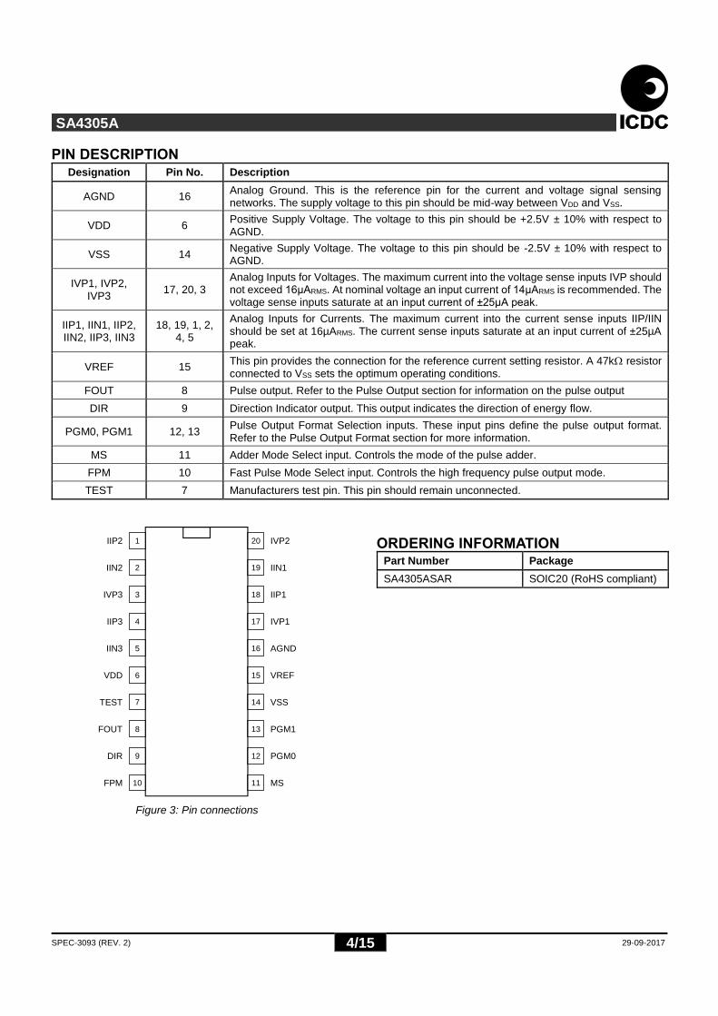
PIN DESCRIPTION Designation Pin No. Description
AGND 16 Analog Ground. This is the reference pin for the current and voltage signal sensing networks. The supply voltage to this pin should be mid-way between VDD and VSS.
VDD 6 Positive Supply Voltage. The voltage to this pin should be +2.5V ± 10% with respect to AGND.
VSS 14 Negative Supply Voltage. The voltage to this pin should be -2.5V ± 10% with respect to AGND.
IVP1, IVP2, IVP3
17, 20, 3 Analog Inputs for Voltages. The maximum current into the voltage sense inputs IVP should not exceed 16μARMS. At nominal voltage an input current of 14μARMS is recommended. The voltage sense inputs saturate at an input current of ±25μA peak.
IIP1, IIN1, IIP2, IIN2, IIP3, IIN3
18, 19, 1, 2, 4, 5
Analog Inputs for Currents. The maximum current into the current sense inputs IIP/IIN should be set at 16µARMS. The current sense inputs saturate at an input current of ±25µA peak.
VREF 15 This pin provides the connection for the reference current setting resistor. A 47k resistor connected to VSS sets the optimum operating conditions.
FOUT 8 Pulse output. Refer to the Pulse Output section for information on the pulse output
DIR 9 Direction Indicator output. This output indicates the direction of energy flow.
PGM0, PGM1 12, 13 Pulse Output Format Selection inputs. These input pins define the pulse output format. Refer to the Pulse Output Format section for more information.
MS 11 Adder Mode Select input. Controls the mode of the pulse adder.
FPM 10 Fast Pulse Mode Select input. Controls the high frequency pulse output mode.
TEST 7 Manufacturers test pin. This pin should remain unconnected.
Figure 3: Pin connections
ORDERING INFORMATION
Part Number Package
SA4305ASAR SOIC20 (RoHS compliant)
1
2
3
4
5
6
7
8
20
19
18
17
16
15
14
13
IIP2
IIN2
IVP3
IIP3
IIN3
VDD
TEST
FOUT
IVP2
IIN1
IVP1
VREF
VSS
PGM1
9
10
12
11
DIR
FPM
PGM0
MS
IIP1
AGND

SPEC-3093 (REV. 2) 5/15 29-09-2017
SA4305A
TERMINOLOGY Anti-Creep Threshold
The anti-creep threshold is defined as the minimum energy
threshold below which no energy is registered and therefore
no pulses are generated on the pulse output.
Positive Energy
Positive energy is defined when the phase difference
between the input signals IIP and IVP is less than 90 degrees
(-90..90 degrees).
Negative Energy
Negative energy is defined when the phase difference
between the input signals IIP and IVP is greater than 90
degrees (90..270 degrees).
Percentage Error*
Percentage error is given by the following formula:
%𝐸𝑟𝑟𝑜𝑟 =𝐸𝑛𝑒𝑟𝑔𝑦 𝑟𝑒𝑔𝑖𝑠𝑡𝑒𝑟𝑒𝑑 − 𝑇𝑟𝑢𝑒 𝐸𝑛𝑒𝑟𝑔𝑦
𝑇𝑟𝑢𝑒 𝐸𝑛𝑒𝑟𝑔𝑦× 100
NOTE: Since the true value cannot be determined, it is
approximated by a value with a stated uncertainty that can be
traced to standards agreed upon between manufacturer and
user or to national standards.
Rated Operating Conditions*
Set of specified measuring ranges for performance
characteristics and specified operating ranges for influence
quantities, within which the variations or operating errors of a
meter are specified and determined.
Specified Measuring Range*
Set of values of a measured quantity for which the error of a
meter is intended to lie within specified limits.
Specified Operating Range*
A range of values of a single influence quantity, which forms
a part of the rated operating conditions.
Limit Range of Operation*
Extreme conditions which an operating meter can withstand
without damage and without degradation of its metrological
characteristics when it is subsequently operated under its
rated operating conditions.
Maximum Rated Mains Current (IMAX)
Maximum rated mains current is the specified maximum
current flowing through the energy meter at rated operating
conditions.
Constant*
Value expressing the relation between the active energy
registered by the meter and the corresponding value of the
test output. If this value is a number of pulses, the constant
should be either pulses per kilowatt-hour (imp/kWh) or watt-
hours per pulse (Wh/imp).
Nominal Mains Voltage (VNOM)
Nominal mains voltage (VNOM) is the voltage specified for the
energy meter at rated operating conditions.
Maximum Channel Energy (EMAX)
The maximum channel energy is defined as the energy
registered on one channel of the SA4305A when 14μARMS
and 16μARMS input current with zero phase shift are applied
to the voltage and current inputs respectively. Both the
voltage and current inputs saturate at an input current
magnitude of 25µA, or at 17.68µARMS when using sine waves.
The maximum input current on each channel is therefore
defined to be 16µARMS, which leaves about 10% headroom to
the saturation point. An additional headroom of 15% is
reserved on the voltage channel to account for mains voltage
fluctuations.
Maximum Output Frequency (FMAX)
The maximum output frequency (FMAX) is the output
frequency when 14μARMS and 16μARMS input current with
zero phase shift are applied to the voltage and current inputs
of all three channels respectively. Both the voltage and
current inputs saturate at an input current magnitude of 25μA,
or at 17.68μARMS when using sine waves. The maximum
input current on any channel is therefore defined to be
16μARMS, which leaves about 10% headroom to the
saturation point. An additional headroom of 15% is reserved
on the voltage channels to account for mains voltage
fluctuations. The nominal output frequency of 1160Hz is
achieved under such conditions.
* IEC 62052-11, 2003. Electricity Metering Equipment (AC) – General Requirements, Test and Test Conditions
– Part 11: Metering Equipment
SPEC-3093 (REV. 2) 6/15 29-09-2017
SA4305A
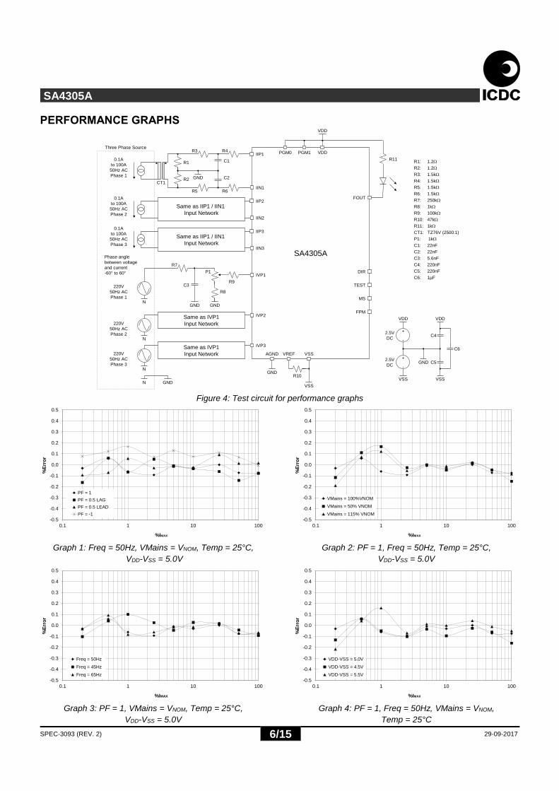
PERFORMANCE GRAPHS
Figure 4: Test circuit for performance graphs
Graph 1: Freq = 50Hz, VMains = VNOM, Temp = 25°C,
VDD-VSS = 5.0V
Graph 3: PF = 1, VMains = VNOM, Temp = 25°C,
VDD-VSS = 5.0V
Graph 2: PF = 1, Freq = 50Hz, Temp = 25°C,
VDD-VSS = 5.0V
Graph 4: PF = 1, Freq = 50Hz, VMains = VNOM,
Temp = 25°C
SA4305A
R6
R4
R10.1A
to 100A
50Hz AC
Phase 1
220V
50Hz AC
Phase 1
IIN1
IIP1
VREF VSS
VSS
FOUT
VDD
VDD
R11
R10
+
-
+
-
GND
GND
VDD
VSS
GND
R1: 1.2
R2: 1.2
R3: 1.5k
R4: 1.5k
R5: 1.5k
R6: 1.5k
R7: 250k
R8: 1k
R9: 100k
R10: 47k
R11: 1k
CT1: TZ76V (2500:1)
P1: 1k
C1: 22nF
C2: 22nF
C3: 5.6nF
C4: 220nF
C5: 220nF
C6: 1µF
CT1
FPM
2.5V
DC
2.5V
DC
VDD
VSS
C4
C5
C6
Phase angle
between voltage
and current
-60 to 60
GND
IVP1
N
N
Three Phase Source
MS
TEST
DIR
AGND
R3
R5
C2
C1
R2
PGM0 PGM1
IIN2
IIP2
Same as IIP1 / IIN1
Input Network
0.1A
to 100A
50Hz AC
Phase 2
IIN3
IIP3
Same as IIP1 / IIN1
Input Network
0.1A
to 100A
50Hz AC
Phase 3
R9C3
GND GND
R7
R8
P1
220V
50Hz AC
Phase 2N
220V
50Hz AC
Phase 3N
Same as IVP1
Input Network
IVP2
Same as IVP1
Input Network
IVP3
-0.5
-0.4
-0.3
-0.2
-0.1
0.0
0.1
0.2
0.3
0.4
0.5
0.1 1 10 100
%E
rro
r
%IMAX
PF = 1
PF = 0.5 LAG
PF = 0.5 LEAD
PF = -1
-0.5
-0.4
-0.3
-0.2
-0.1
0.0
0.1
0.2
0.3
0.4
0.5
0.1 1 10 100
%E
rro
r
%IMAX
Freq = 50Hz
Freq = 45Hz
Freq = 65Hz
-0.5
-0.4
-0.3
-0.2
-0.1
0.0
0.1
0.2
0.3
0.4
0.5
0.1 1 10 100
%E
rro
r
%IMAX
VMains = 100%VNOM
VMains = 50% VNOM
VMains = 115% VNOM
-0.5
-0.4
-0.3
-0.2
-0.1
0.0
0.1
0.2
0.3
0.4
0.5
0.1 1 10 100
%E
rro
r
%IMAX
VDD-VSS = 5.0V
VDD-VSS = 4.5V
VDD-VSS = 5.5V

SPEC-3093 (REV. 2) 7/15 29-09-2017
SA4305A
FUNCTIONAL DESCRIPTION Theory of Operation
The SA4305A includes all the required functions for three
phase power and energy measurement. Three pairs of
identical AD converters sample the three phase voltage and
current input signals. The three pairs of digital signals,
accurately representing the voltage and current inputs, are
multiplied using digital multiplication. The output of each
multiplier represents the instantaneous power on each
channel. The three channels are added together and the
pulse generation circuit creates a pulse output where the
instantaneous frequency is proportional to the instantaneous
power measured. The addition of the three channels can be
programmed to arithmetic or absolute mode. The arithmetic
mode will take the direction of energy flow into account while
the absolute mode will ignore it.
For given voltage and current signals the instantaneous
power is calculated by:
𝑝(𝑡) = 𝑣(𝑡) × 𝑖(𝑡)
𝑝(𝑡) = 𝑉𝑀 cos(𝜔𝑡 + 𝜃) × 𝐼𝑀 cos(𝜔𝑡 + 𝜓)
Let 𝜙 = 𝜃 − 𝜓, and 𝑉𝑅𝑀𝑆 =𝑉𝑀
√2 and 𝐼𝑅𝑀𝑆 =
𝐼𝑀
√2 then
𝑝(𝑡) = 𝑉𝑀 cos(𝜔𝑡 + 𝜃) × 𝐼𝑀 cos(𝜔𝑡 + 𝜃 − 𝜙)
𝑝(𝑡) = 𝑉𝑅𝑀𝑆𝐼𝑅𝑀𝑆(cos 𝜙 + cos(2(𝜔𝑡 + 𝜃) − 𝜙))
where
p(t) is the instantaneous power,
v(t) is the instantaneous voltage signal,
i(t) is the instantaneous current signal,
VM is the amplitude of the voltage signal,
IM is the amplitude of the current signal,
is the phase angle of the voltage signal and
is the phase angle of the current signal.
The instantaneous power output is integrated over time to
obtain the energy by simply counting the output pulses. This
removes the double mains frequency component
cos(2(t+)-) and the average output pulse rate is therefore
equivalent to
𝑃 =1
𝑇∫ 𝑝(𝑡)𝑑𝑡
𝑇
0
𝑃 = 𝑉𝑅𝑀𝑆𝐼𝑅𝑀𝑆 cos 𝜙
where
P is the average power and
cos is the power factor.
Linearity
The SA4305A is a CMOS integrated circuit, which performs
power/energy calculations across a dynamic range of 500:1
to an accuracy that exceeds the IEC62053 specification.
Analog Inputs
The input circuitry of the current and voltage sensor inputs is
illustrated in Figure 5. These inputs are protected against
electrostatic discharge through clamping diodes. The
feedback loops from the outputs of the amplifiers AI and AV
generate virtual short circuits between IIP and IIN as well as
IVP and AGND. The current sense inputs (IIP and IIN) are
identical and balanced. The AD converters convert the
signals on the voltage and current sense inputs to a digital
format for further processing. All internal offsets are
eliminated through the use of various cancellation
techniques.
Figure 5: Analog input configuration
Digital Outputs
The calculations required for power and energy are
performed and the result is converted to pulses on the FOUT
pulse output. The instantaneous output frequency on the
pulse output is proportional to the instantaneous active power
consumption measured. The pulse output is intended for
interfacing the SA4305A to a microcontroller or similar pulse
processing circuit.
Anti-Creep Threshold
An integrated anti-creep function prevents any output pulses
from a channel appearing on the pulse output if the energy
measured on that channel is less than 0.02% of EMAX, where
EMAX is the energy registered when the input currents for
voltage and current are 14μARMS and 16μARMS with zero
phase shift respectively. The individual per channel creep
AI
IIN
IIP
VDD
VSS
VDD
VSS
AV
IVP
VDD
VSS
AGND
VOLTAGE
SENSOR
INPUT
CURRENT
SENSOR
INPUT
CURRENT
CHANNEL
ADC
VOLTAGE
CHANNEL
ADC

SPEC-3093 (REV. 2) 8/15 29-09-2017
SA4305A
feature improves the device performance in missing phase
scenarios. It also allows the device to be used in three phase
three wire meters where one channel of the device is unused.
Reverse Energy Flow Indication
The SA4305A assesses the phase difference between the
voltage and current channel signals to determine the direction
of energy flow. If the overall energy flow is negative the
reverse energy indicator is activated. This facility is designed
to detect the wrongful connection or possible tampering of the
meter. If the adder is programmed to absolute mode the
energy flow direction information is lost. The operation of the
direction output is fully described in the Output Signals
section.
Starting Current
The SA4305A generates pulses on the pulse outputs for an
input power greater than 0.02% of EMAX. This is to comply
with the IEC requirement where the meter is required to
generate pulses for currents greater than 0.4%Ib.
Power-On Reset
The SA4305A has a power-on reset circuitry that activates
whenever the voltage between VDD and VSS is less than
3.6V ± 8%.
Power Consumption
The power consumption of the SA4305A integrated circuit is
less than 50mW.
Compatibility with SA2005F
The SA4305A can be used as a functionally compatible
replacement for the SA2005F by simply leaving the pins FPM
and MS unconnected. It should however be noted that the
value of the reference resistor on the VREF pin has to be
changed from 24k to 47k
INPUT SIGNALS Voltage Reference (VREF)
A bias resistor of 47k sets optimum bias and reference
conditions on chip. Calibration of the SA4305A should be
done on the voltage inputs and not on the VREF input.
Current Sense Inputs (IIP1/IIN1, IIP2/IIN2, IIP3/IIN3)
Figure 6 shows the typical connections for the current sensor
input for one channel. The circuit has to be repeated for the
other two channels. At maximum rated mains current (IMAX)
the resistor values should be selected for input currents of
16µARMS. The current sense inputs saturate at an input
current of ±17.6μARMS (±25μAPEAK), so this allows about 10%
headroom until saturation occurs.
The resistors RA and RB form the current transformers
termination resistor. The reference level is connected in the
centre of the termination resistor to achieve purely differential
input currents. The voltage drop across the termination
resistors at maximum rated mains current (IMAX) should be in
the order of 100mVRMS. The termination resistance should
also be significantly smaller than the DC resistance of the
current transformers secondary winding.
Figure 6: Current sense input configuration
The resistors R1 to R4 define the current flowing into the
device. For best performance the SA4305A requires anti-
alias filters on the current sense inputs. These filters are
realized by means of the capacitors C1 and C2. The typical
cut-off frequency of these filters should be between 10kHz
and 20kHz. The optimum input network is achieved by setting
the input resistors equal, i.e. setting R1 = R2 = R3 = R4 = RC.
This sets the equivalent resistance associated with each
capacitor to RC/2.
Voltage Sense Inputs (IVP1, IVP2, IVP3)
Figure 7 shows the voltage sense input configuration for one
channel. The circuit is identical for the other two channels.
The voltage sense input saturates at an input current of
±17.6μARMS (±25μAPEAK). The current into the voltage sense
input should be set at 14μARMS at nominal mains voltage
(VNOM) to allow for a mains voltage variation of up to +25%
without saturating the voltage sense input.
Figure 7: Voltage sense input configuration
For best performance the SA4305A also requires an anti-
alias filter on the voltage sense inputs. Referring to Figure 7,
the capacitor C1 is used to both implement the anti-alias filter
as well as compensating for any phase shift caused by the
current transformer. The resistor R4 defines the input current
into the device. The optimum input network is achieved by
setting R4 in the order of 100k. If R4 is made too large the
capacitor C1 will be very small and the accuracy of the phase
R3
R1
RA
IIN
IIP
GND
CT1Current In
IMAX
16µARMS
R4
R2
RBCurrent Out
C1
C2
R4
R3
IVP
GND
C1
R2R1
GND
VNOM
14µARMS
Voltage In
Neutral
GND
R5
P1
(P1 + R5) << R4 << (R1 + R2 + R3)

SPEC-3093 (REV. 2) 9/15 29-09-2017
SA4305A
compensation could be affected by stray capacitances. The
potentiometer P1 is used for calibration purposes.
Pulse Output Format Selection
(PGM0, PGM1, FPM)
The pulse output programming inputs PGM0, PGM1 and
FPM define the representation of energy measured by the
device on FOUT. Table 1 below shows the difference
between the various modes. Mode 4 basically bypasses the
adder and the individual pulses of each channel of the device
are output directly. The pulse width allows the allocation of
pulses to specific channels. Refer to Table 1 for details on the
pulse output format in each mode.
Adder Mode Selection (MS)
The energy addition of the three channels may be set to
arithmetic or absolute mode using the MS input. If MS is tied
to VSS the adder operates in arithmetic mode. In this mode
the direction of energy flow on each channel is taken into
account during addition. Negative energy is thus subtracted
from positive energy in the addition process. If MS is tied to
VDD the adder operates in absolute mode. The direction of
energy flow on each channel is ignored and assumed to be
positive. The reversal of a channel will therefore not affect the
pulse output rate. This can be used as an anti-tamper feature.
The MS input is ignored in pulse output mode 4 where the
pulses on each channel are output individually.
OUTPUT SIGNALS Pulse Output (FOUT)
The average nominal output frequency of the pulse output in
mode 3 is given by
𝑓𝐹𝑂𝑈𝑇−𝑀𝑂𝐷𝐸3 = 1160 ×
|𝐼𝑉1 × 𝐼𝐼1 × cos 𝜙1 + 𝐼𝑉2 × 𝐼𝐼2 × cos 𝜙2 + 𝐼𝑉3 × 𝐼𝐼3 × cos 𝜙3
3 × 14 × 16|
…(1)
where
IVX and IIX are the analog input currents in µARMS on the
voltage and current sense inputs on channel X and
X is the phase angle between the current and voltage signals
on channel X.
The pulse output rate in modes 0, 1 and 2 is 18 times lower
than in mode 3 and 4. The integrated anti-creep threshold
ensures that no output pulses are generated from a channel
if the energy measured on that channel is below 0.02% of
EMAX, where EMAX is the energy registered on the channel when the voltage and current sense input currents are
14μARMS and 16μARMS respectively. The power-up state of
the pulse output is dependent on the pulse output mode that
has been selected.
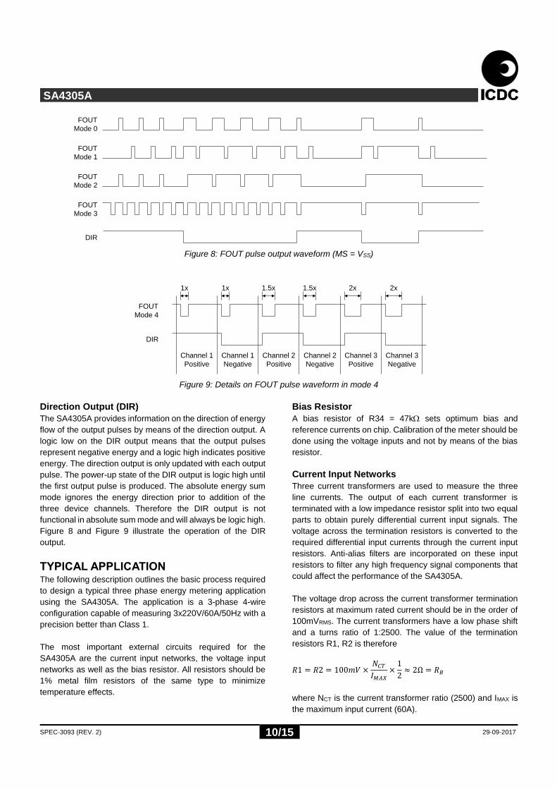
Figure 8 shows the output waveform of FOUT for the pulse
output modes 0 to 3. Modes 0, 1 and 2 allow direct sensing
of the total energy flow direction from the pulse output. Note
that the pulse output timing and rate differ in mode 3. This
fact has been omitted in Figure 8 for the sake of clarity.
Setting FPM, PGM0 and PGM1 to VDD will set the pulse
output mode to mode 4. In this mode the internal pulse adder
is bypassed. Each channel’s pulses appear independently on
FOUT. The pulse width allows the output pulses to be
allocated to a specific channel. The pulses from channel 2
are 1.5x the width of the channel 1 pulses while those of
channel 3 are 2x the width of the channel 1 pulses. Pulse
output mode 4 is illustrated in Figure 9.
Table 1: Pulse output characteristics for various modes
Mode FPM PGM1 PGM0 Frequency
at rated conditions
Forward energy pulse
polarity
Reverse energy pulse
polarity
Pulse on direction change
Forward energy
pulse width
Reverse energy
pulse width
0 X 0 0 64.4Hz Positive Positive Yes 1.15ms 3.44ms
1 X 0 1 64.4Hz Positive Negative Yes 1.15ms 1.15ms
2 X 1 0 64.4Hz Positive Negative No 1.15ms 1.15ms
3 0 1 1 1160Hz Negative Negative Yes 71.7µs 71.7µs
4 1 1 1 386Hz per
channel Negative Negative Yes
71.7µs Ch1 108µs Ch2 143us Ch3
71.7µs Ch1 108µs Ch2 143us Ch3
Notes: 1 Pin values for FPM, PGM0 and PGM1, 0 means pin is connected to VSS, 1 means pin is connected to VDD, X means the pin state is irrelevant
2 Pulse rate of modes 3 and 4 is 18 times higher as that of modes 0, 1 and 2 3 Pulse frequencies are based on nominal device gain 4 Pulse widths are based on nominal oscillator frequency
SPEC-3093 (REV. 2) 10/15 29-09-2017
SA4305A
Figure 8: FOUT pulse output waveform (MS = VSS)
Figure 9: Details on FOUT pulse waveform in mode 4
Direction Output (DIR)
The SA4305A provides information on the direction of energy
flow of the output pulses by means of the direction output. A
logic low on the DIR output means that the output pulses
represent negative energy and a logic high indicates positive
energy. The direction output is only updated with each output
pulse. The power-up state of the DIR output is logic high until
the first output pulse is produced. The absolute energy sum
mode ignores the energy direction prior to addition of the
three device channels. Therefore the DIR output is not
functional in absolute sum mode and will always be logic high.
Figure 8 and Figure 9 illustrate the operation of the DIR
output.
TYPICAL APPLICATION The following description outlines the basic process required
to design a typical three phase energy metering application
using the SA4305A. The application is a 3-phase 4-wire
configuration capable of measuring 3x220V/60A/50Hz with a
precision better than Class 1.
The most important external circuits required for the
SA4305A are the current input networks, the voltage input
networks as well as the bias resistor. All resistors should be
1% metal film resistors of the same type to minimize
temperature effects.
Bias Resistor
A bias resistor of R34 = 47k sets optimum bias and
reference currents on chip. Calibration of the meter should be
done using the voltage inputs and not by means of the bias
resistor.
Current Input Networks
Three current transformers are used to measure the three
line currents. The output of each current transformer is
terminated with a low impedance resistor split into two equal
parts to obtain purely differential current input signals. The
voltage across the termination resistors is converted to the
required differential input currents through the current input
resistors. Anti-alias filters are incorporated on these input
resistors to filter any high frequency signal components that
could affect the performance of the SA4305A.
The voltage drop across the current transformer termination
resistors at maximum rated current should be in the order of
100mVRMS. The current transformers have a low phase shift
and a turns ratio of 1:2500. The value of the termination
resistors R1, R2 is therefore
𝑅1 = 𝑅2 = 100𝑚𝑉 ×𝑁𝐶𝑇
𝐼𝑀𝐴𝑋×
1
2≈ 2Ω = 𝑅𝐵
where NCT is the current transformer ratio (2500) and IMAX is
the maximum input current (60A).
FOUT
Mode 0
FOUT
Mode 1
FOUT
Mode 2
FOUT
Mode 3
DIR
FOUT
Mode 4
DIR
Channel 1
Positive
Channel 1
Negative
Channel 2
Positive
Channel 2
Negative
Channel 3
Positive
Channel 3
Negative
1x 1x 1.5x 1.5x 2x 2x

SPEC-3093 (REV. 2) 11/15 29-09-2017
SA4305A
The four current input resistors (R3, R4, R5, R6) should be of
equal size to optimize the input networks low pass filtering
characteristics, so the values can be calculated as follows:
𝑅3 = 𝑅4 = 𝑅5 = 𝑅6 =𝐼𝑀𝐴𝑋
𝑁𝐶𝑇×
𝑅𝐵
2 × 16𝜇𝐴= 1.5𝑘Ω = 𝑅𝐶
For optimum performance the cut-off frequency of the anti-
alias filter should be between 10kHz and 20kHz. The
equivalent resistance associated with each capacitor is RC/2
so the capacitor values should be in the order of
𝐶1 = 𝐶2 =1
𝜋𝑓𝐶𝐼𝑅𝐶=
1
𝜋 × 10𝑘𝐻𝑧 × 1.5𝑘Ω≈ 22𝑛𝐹 = 𝐶𝐶
where fCI is the cut-off frequency of the anti-alias filter of the
current input network.
The current input networks for channel 2 and channel 3 are
identical.
Voltage Input Networks
The voltage sense inputs should optimally be set to an input
current of 14μARMS at VNOM (220V). The mains voltage is
divided by means of a voltage divider to a lower voltage that
is converted to the required input current by means of the
input resistor. Once again an anti-alias filter is required to
remove any high frequency signals that could affect the
performance of the SA4305A. The phase shift of the current
transformers is compensated by means of this anti-alias filter
as well, by purposefully increasing the cut-off frequency.
The input resistor R22 sets the current input into the device.
This resistor should not be too large else the capacitor for the
anti-alias filter will be quite small which could cause
inaccurate phase shift due to parasitic capacitances.
Therefore R22 = 100k is chosen and the voltage at the
centre of the trimpot should be 1.4V (14μA x 100k). The
calibration range of the voltage input network should be about
±15% to ensure that all component tolerances can be catered
for, so the total tuning range can be set to ±0.22V. Therefore
the voltage across the trimpot and R23 is 1.62V. Choosing a
1k trimpot results in
𝑅23 =1𝑘Ω
(2 × 0.22)× (1.62 − 2 × 0.22) ≈ 2.7𝑘Ω
The effect of R22 can be ignored in the above equation, given
the fact that R22 is significantly larger than P1 and R23. Now
let RA = R19 + R20 + R21 and
𝑅𝐴 = (𝑃1 + 𝑅23) × (220𝑉
1.62𝑉− 1) ≈ 499𝑘Ω
so choose R19 = R20 = 200k and R21 = 100k.
The cut-off frequency of the anti-alias filter is adjusted so that
the phase shift of the voltage input network is identical to the
sum of the phase shifts of the current transformer and the
current input network. The phase shift of the current input
network is
𝜙𝐼𝐼 = − tan−1(𝜋𝑅𝐶𝐶𝐶 × 50𝐻𝑧) ≈ −0.297°
The phase shift required on the voltage input network is
therefore
𝜙𝐼𝑉 = 𝜙𝐼𝐼 − 𝜙𝐶𝑇 = −0.297° + 0.09° = −0.207°
where CT is the phase shift of the current transformer which
is typically about 0.09 degrees for a good quality current
transformer. Neglecting R19, R20, R21 and R22 because all
these resistors are significantly larger than P1 and R23 the
capacitance required to achieve the -0.207 degree phase
shift is
𝐶7 =|tan 𝜙𝐼𝑉|
2𝜋(𝑃1 + 𝑅23) × 50𝐻𝑧≈ 3.3𝑛𝐹
resulting in a cut-off frequency of
𝑓𝐶𝑉 =1
2𝜋(𝑃1 + 𝑅23) × 𝐶7≈ 13𝑘𝐻𝑧
The value of the cut-off frequency of the voltage input network
is less critical than that of the current input network because
the dynamic range of the voltage input is small. A cut-off
frequency between 10kHz and 25kHz is acceptable.
The voltage input networks for channel 2 and channel 3 are
identical
Device Setup
Depending on the desired output pulse format the four device
setup pins (PGM0, PGM1, MS and FPM) need to be
configured. These pins should be connected directly to either
VDD or VSS. The MS and FPM inputs have internal pull-down
resistors and may therefore be left floating. This will be
equivalent to connecting the pin to VSS. The TEST pin should
be left floating.

SPEC-3093 (REV. 2) 12/15 29-09-2017
SA4305A
Figure 10: Typical application circuit
Table 2: Component list for typical application
Symbol Description
U1 Energy metering device,
SA4305ASAR
R1, R2, R7, R8,
R13, R14 Resistor, 2, 1%, metal film
R3, R41, R5, R61,
R9, R101, R11, R121,
R15, R161, R17, R181
Resistor, 1.5k, 1%, metal film
R19, R20, R24, R25,
R29, R30 Resistor, 200k, 1%, metal film
R21, R221, R26,
R271, R31, R321 Resistor, 100k, 1%, metal film
Symbol Description
R23, R28, R33 Resistor, 2.7k, 1%, metal film
R341 Resistor, 47k, 1%, metal film
P1, P2, P3 Trim-pot, 25 turns, 1k
C1, C2, C3, C4, C5,
C6 Capacitor, 22nF, ceramic
C7, C8, C9 Capacitor, 3.3nF, ceramic
C102, C112 Capacitor, 220nF, ceramic
C122 Capacitor, 1μF, ceramic
CT1, CT2, CT3 Current transformer, 60A,
1:2500
Note 1: Resistors R4, R6, R10, R12, R16, R18, R22, R27, R32 and R34 must be positioned as close as possible
to the respective device pins
Note 2: Capacitors C10, C11 and C12 must be positioned as close as possible to the VDD and VSS power supply
pins
12
6
14
15
PGM0
VDD
VSS
VREF
IIP1
IIN1
SA4305A
U1
DIR
FOUT
IVP3
IVP2
IVP1
AGND16
17
20
3
8
9
FPM10
PGM113
18
19CT1
R2 2C2
R1 2
R5 R6
R3 R4
1.5k 1.5k
1.5k 1.5k
C1 22nF
22nF
1
2CT2
R8 2C4
R7 2
R11 R12
R9 R10
1.5k 1.5k
1.5k 1.5k
C3 22nF
22nF
4
5CT3
R14 2C6
R13 2
R17 R18
R15 R16
1.5k 1.5k
1.5k 1.5k
C5 22nF
22nF
IIP2
IIN3
R34
47k-2.5V
+2.5V
R24
200k
R29
200k
R19
200k
R25
200k
R30
200k
R20
200k
R26
100k
R31
100k
R21
100k
R27
100k
R32
100k
R22
100k
P2 1k
P3 1k
P1 1k
R28
2.7k
R33
2.7k
R23
2.7k
0V
0V
MS11
IIN2
LIVE 1 IN
LIVE 2 IN
LIVE 3 IN
NEUTRAL
0V
IIP3
LIVE 3 OUT
LIVE 2 OUT
LIVE 1 OUT
C73.3nF
C83.3nF 3.3nF
C9
0V
C10
220nF
C11
220nF
C12
1µF
+2.5V
-2.5V
0V
0V
0V
0V
TEST7
Pulse Processing Circuit
e.g. Microcontroller
+2.5V or -2.5V
+2.5V or -2.5V
+2.5V or -2.5V or floating
+2.5V or -2.5V or floating

SPEC-3093 (REV. 2) 13/15 29-09-2017
SA4305A
PACKAGE DIMENSIONS
SOIC20 Package Dimensions are shown in inches

SPEC-3093 (REV. 2) 14/15 29-09-2017
SA4305A
NOTES
SPEC-3093 (REV. 2) 15/15 29-09-2017
SA4305A
DISCLAIMER The information contained in this document is confidential and proprietary to Integrated Circuit Design Centre (Pty) Ltd ("ICDC"),
a division of South African Micro-Electronic Systems (Pty) Ltd ("SAMES"), and may not be copied or disclosed to a third party, in
whole or in part, without the express written consent of ICDC. The information contained herein is current as of the date of
publication; however, delivery of this document shall not under any circumstances create any implication that the information
contained herein is correct as of any time subsequent to such date. ICDC does not undertake to inform any recipient of this
document of any changes in the information contained herein, and ICDC expressly reserves the right to make changes in such
information, without notification, even if such changes would render information contained herein inaccurate or incomplete. ICDC
makes no representation or warranty that any circuit designed by reference to the information contained herein, will function
without errors and as intended by the designer.
Any sales or technical questions may be sent to our support e-mail address:
For the latest updates on datasheets, please visit our web site:
http://www.sames.co.za.
INTEGRATED CIRCUIT DESIGN CENTRE (PTY) LTD
a division of
SOUTH AFRICAN MICRO-ELECTRONIC SYSTEMS (PTY) LTD
Tel: 012 333 6021
Tel Int: 00 27 12 333 6021
Fax: 012 333 6393
Fax Int: 00 27 12 333 6393
PO BOX 15888
LYNN EAST 0039
REPUBLIC OF SOUTH AFRICA
UNIT 4, PERSEQUOR CLOSE
49 DE HAVILLAND CRESCENT
PERSEQUOR TECHNOPARK
LYNNWOOD, PRETORIA
REPUBLIC OF SOUTH AFRICA