ig1602n-6gnn-218 rev:a page - illumin.com.t · ig1602n-6gnn-218 rev:a page: 1 /28 fstn module...
TRANSCRIPT

IG1602N-6GNN-218 REV:A Page: 1 /28
FSTN Module Specification IG1602N-6GNN-218
1. OUTLINE DRAWING ...................................................................................................................2 2. FEATURE .......................................................................................................................................3 3. ABSLUTE MAXIMUN RATINGS ................................................................................................4 4. DC ELETRICAL CHARACTERISTICS......................................................................................4 5. PIN DEFINITION...........................................................................................................................5 6. INS TR UC TION DESC RIPTIO N ..................................................................................................6
6.1 Instructions ...........................................................................................................................6 6.2 Reset Function ...................................................................................................................17 6.3 Initializing by Instruction ...................................................................................................17
7. IIC Interface Function Description ............................................................................................12 8. APPLICATION CIRCUIT ...........................................................................................................15
8.1 Timing Characteristics ......................................................................................................15 8.2 APPLICATION CIRCUIT .................................................................................................16
9. LCM NUMBERING SYSTEM ...................................................................................................17 10. HISTORY......................................................................................................................................18 11. ELECTRO-OPTICAL UNITs ......................................................................................................19
11.1 Mechanical Specification..................................................................................................19 11.2 Optical Definitions .............................................................................................................19 11.3 Reliability ............................................................................................................................21 11.4 Precautions in Use of LCM..............................................................................................21 11.4.1 Handing of LCM.............................................................................................................21 11.4.2 Storage............................................................................................................................21

IG1602N-6GNN-218 REV:A Page: 2 /28
1. OUTLINE DRAWING
IG1602N-6GNN-218 REV:A Page: 3 /28
2. FEATURE
General Specification l Display Format: 16 Characters X 2
line l Character Size: 2.460(W)
X4.76(H)mm l LCM View Area: 50.00(W)
X16.00(H)mm l General Dimensions: 54.80(W)
X26.00(H) X 2.7 MAX(T)mm l LCD Type: STN(Gray) Polarizer Mode:
Transflective(低半透)/Positive l Connection: COG+FPC l Driving Method: 1/16DUTY, 1/5BIAS,
VOP 5.0V, VDD 3V~5.5V. l View Angle: 6 O’clock l Operating Temp: -20 To +70ºC
Storage Temp: -30 To +80ºC l Single CHIP : ST7032i

IG1602N-6GNN-218 REV:A Page: 4 /28
3. ABSLUTE MAXIMUN RATINGS
Item Symbol Conditions Min. Max. Unit Power supply Voltage VDD - -0.3 +7.0 V
LCD drive Supply voltage VDD-VO - 7.0-VSS -0.3+VSS V
Input voltage VIN - -0.3 VDD +0.3 V Operating temperature TOPR - -20 70 °C
Storage temperature TSTG - -30 80 °C Humidity*1 HD - - - %RH
4. DC ELETRICAL CHARACTERISTICS
VDD=4.5V-5.5V,VSS=0V,TA=25°C Item Symbol Condition Min. Typ. Max. Unit
Logic Supply voltage VDD - 2.7 3.3 5.5 V “H” input voltage VIH - 2.7 - VDD V “L” input voltage VIL - -0.3 - 0.8 V
“H” output voltage VOH - 3.8 - VDD V “L” output voltage VOL - - - 0.8 V
Supply current IDD VDD=3.3V - 0.5 1.0 mA LCD driving voltage VOP Vlcd~VSS 2.7 - 7.0 V

IG1602N-6GNN-218 REV:A Page: 5 /28
5. PIN DEFINITION
NO SYMBOL I/O FUNCTION 1 RESET P Low active,RESET pin must be fixed to VDD. 2 SCLK I/O CLOCK bit for IIC 3 SDATA I/O DATA bit for IIC 4 GND P GND (0V) 5 VDD P DC +3V~ +5.0V 6 CAP(+) -- 7 CAP(-) --
For voltage booster circuit(VDD-VSS) External capacitor about 0.1uF~4.7uF
8 V0 P DC +5V, or Connect a capacitor between this and VDD

IG1602N-6GNN-218 REV:A Page: 6 /28
6. Instruction Description
6.1 Instructions There are four categori es of i ns tructi ons that: �� Desi g na te S T7032 f u nc tio n s, s uc h as dis pl a y f or m a t, d ata len g t h, etc. �� Set in ter nal R A M a d dre s s e s �� Per f or m d at a tra n sfe r wit h in ter n al R A M �� O t her s
? instruction table at “Extension mode” (when “EXT” opti on pin connect to VSS, the i nstructi on set foll ow below table)
Instruction Code Instruction Execution Time
Instruction RS
R/W
DB7
DB6
DB5
DB4
DB3
DB2
DB1
DB0
Description OSC=
380KHz OSC= 540kHz
OSC= 700KHz
Clear Display
0
0
0
0
0
0
0
0
0
1 Write "20H" to DDRAM. and set
DDRAM address to "00H" from AC 1.08 ms
0.76 ms
0.59 ms
Return Home
0
0
0
0
0
0
0
0
1
x Set DDRAM address to "00H" from AC and return cursor to its original position if shifted. The contents of DDRAM are not changed.
1.08 ms
0.76 ms
0.59 ms
Entry Mode Set
0
0
0
0
0
0
0
1 I/D
S Sets cursor move direction and specifies display shift. These operations are performed during data write and read.
26.3 us
18.5 us
14.3 us
Display ON/OFF
0
0
0
0
0
0
1
D
C
B
D=1:entire display on C=1:cursor on B=1:cursor position on
26.3 us
18.5 us
14.3 us
Function Set
0
0
0
0
1 DL
N DH
*0
IS DL: interface data is 8/4 bits N: number of line is 2/1 DH: double height font IS: instruction table select
26.3 us
18.5 us
14.3 us
Set DDRAM address
0
0
1
AC6
AC5
AC4
AC3
AC2
AC1
AC0 Set DDRAM address in address
counter 26.3 us
18.5 us
14.3 us
Read Busy flag and address
0
1 BF
AC6
AC5
AC4
AC3
AC2
AC1
AC0
Whether during internal operation or not can be known by reading BF. The contents of address counter can also be read.
0
0
0
Write data to RAM
1
0
D7
D6
D5
D4
D3
D2
D1
D0 Write data into internal RAM
(DDRAM/CGRAM/ICONRAM) 26.3 us
18.5 us
14.3 us
Read data from RAM
1
1
D7
D6
D5
D4
D3
D2
D1
D0 Read data from internal RAM
(DDRAM/CGRAM/ICONRAM) 26.3 us
18.5 us
14.3 us
Note * : this bit is for test command , and must always set to “0”

IG1602N-6GNN-218 REV:A Page: 7 /28
0
0
0
0
0
0
0
1
0
0
0
0
0
0
1
X
0
0
0
0
0
1
I/D
S
Instruction table 0(IS=0)
Cursor or Display Shift
0
0
0
0
0
1 S/C
R/L
x
x S/C and R/L: Set cursor moving and display shift control bit, and the direction, without changing DDRAM data.
26.3 us
18.5 us
14.3 us
Set CGRAM
0
0
0
1 AC5
AC4
AC3
AC2
AC1
AC0 Set CGRAM address in address
counter 26.3 us
18.5 us
14.3 us
Instruction table 1(IS=1)
Internal OSC frequency
0
0
0
0
0
1 BS
F2
F1
F0 BS=1:1/4 bias BS=0:1/5 bias F2~0: adjus t internal OSC frequency for FR frequency.
26.3 us
18.5 us
14.3 us
Set ICON address
0
0
0
1
0
0
AC3
AC2
AC1
AC0 Set ICON address in address
counter. 26.3 us
18.5 us
14.3 us
Power/ICON control/Contr ast set
0
0
0
1
0
1 Ion
Bon
C5
C4
Ion: ICON display on/off Bon: set boos ter circuit on/off C5,C4: Contrast set for internal follower mode.
26.3 us
18.5 us
14.3 us
Follower control
0
0
0
1
1
0
Fon
Rab
2
Rab
1
Rab
0 Fon: set follower circuit on/off Rab2~0: select follower amplified ratio.
26.3 us
18.5 us
14.3 us
Contrast set
0
0
0
1
1
1 C3
C2
C1
C0 Contrast set for internal follower
mode. 26.3 us
18.5 us
14.3 us
l Clear Displ a y
RS R/W
0 0
DB7 DB6 DB5 DB4 DB3 DB2 DB1 DB0
Clear all the di splay data by writi ng "20H" (space code) to all DDRA M address, and set DDRA M address to
"00H" i nto AC (address counter) . Return cursor to the ori ginal s tatus, namely , bri ng the cursor to the l eft edge
on firs t li ne of the display . Make entry mode increment (I/D = "1").
l Ret u r n H o m e
RS R/W
0 0
DB7 DB6 DB5 DB4 DB3 DB2 DB1 DB0
Return Ho me is cursor return ho me instructi on. Set DDRA M address to "00H" i nto the address counter .
Return cursor to i ts ori ginal si te and return display to i ts ori ginal s tatus , if shi fted. Contents of DDRAM do not
change.
l E ntr y M o de Set
RS R/W
0 0
DB7 DB6 DB5 DB4 DB3 DB2 DB1 DB0
Set the moving direc ti on of cursor and display.
? I /D : I ncre m e n t / d ecre m e n t of D D RA M ad dr ess (c urs o r or bl i nk )

IG1602N-6GNN-218 REV:A Page: 8 /28
W hen I/D = "High", cursor /bli nk moves to ri ght and DDRA M address is i ncreased by 1.
W hen I/D = "Low", cursor /bli nk moves to l eft and DDRA M address is decreased by 1.
* CGRA M operates the sa me as DDRA M, when read from or write to CGRA M.
? S: S hift o f e ntire dis pl a y W hen DDRA M read (CG RAM read/wri te) operati on or S = "Low", shi ft of enti re display i s not per formed. If
S = "High" and DDRA M wri te operati on, shift of enti re di splay is per formed according to I/D value ( I/D = "1":
shi ft l eft, I/D = "0" : shift ri ght).
S I/D Description
H
H Shi ft the di splay to the l eft
H
L
Shi ft the di splay to the ri ght

IG1602N-6GNN-218 REV:A Page: 9 /28
0
0
0
0
1
D
C
B
0
0
0
1
S/C
R/L
X
X
l Dis play ON/ O F F
RS R/W
0 0
DB7 DB6 DB5 DB4 DB3 DB2 DB1 DB0
Control display/cursor /bli nk ON/OFF 1 bi t regi s ter. ? D : Dis play O N/ O F F co n tr ol bi t
W hen D = "High", enti re di splay is turned on.
W hen D = "Low", di splay is turned off, but di splay data is remained in DDRAM.
? C : C urs o r ON/ O F F c o ntr ol bi t W hen C = "High", cursor is turned on.
W hen C = "Low", cursor is di sappeared in current di splay, but I/D regis ter re mains its data.
? B : C urs o r Bl in k ON/ O F F c ontr ol bi t W hen B = "High", cursor bli nk is on, that per forms al ternate between all the high data and di splay
character at the cursor positi on.
W hen B = "Low", bli nk i s off.
Cursor
Alternating display
Every
64 frames
l C urs or or Dis play S hif t
RS R/W
0 0
DB7 DB6 DB5 DB4 DB3
DB2 DB1
DB0

IG1602N-6GNN-218 REV:A Page: 10 /28
0
0
1
DL
N
DH
0
IS
? S/C: Scr ee n/C ur s or select bi t
W hen S/C=”High”, Screen i s controll ed by R/L bi t.
W hen S/C=”Low”, Cursor i s controll ed by R/L bi t.
? R/L : Right/ L eft W hen R/L=”High”, set direc ti on to ri ght.
W hen R/L=”Low”, set direc ti on to l eft. Wi thout writi ng or reading of di splay data, shi ft ri ght/l eft cursor posi ti on or di splay . Thi s i nstruc ti on is used to
correc t or search di splay data. Dur ing 2-li ne mode di splay , cursor moves to the 2nd li ne after 40th digi t of 1st
line. Note that di splay shift is performed simul taneous l y in all the li ne. W hen di splayed
data is shi fted repeatedl y, each li ne shifted i ndivi dually . W hen di splay shi ft is per formed, the contents of
address counter are
not changed.
S/C R/L Description AC Value L L Shi ft cursor to the l eft AC=AC-1 L H Shi ft cursor to the ri ght AC=AC+1 H L Shi ft di splay to the l eft. Cursor foll ows the di splay shi ft AC=AC H H Shi ft di splay to the ri ght. Cursor foll ows the di splay shi ft AC=AC
l F u n cti o n Set
RS R/W
0 0
DB7 DB6 DB5 DB4 DB3 DB2 DB1 DB0

IG1602N-6GNN-218 REV:A Page: 11 /28
? D L : In ter fa c e dat a le ngt h co n tr ol bi t
W hen DL = "High", it means 8-bi t bus mode wi th MPU.
W hen DL = "Low", i t means 4-bi t bus mode wi th MPU. So to speak, DL i s a signal to selec t 8-bit or 4-bi t
bus mode.
W hen in 4-bit bus mode, it needs to trans fer 4-bi t data by two times.
? N : Dis play lin e n u m b er co n tr ol bi t W hen N = "High", 2-li ne di splay mode i s set.
W hen N = "Low", i t means 1-li ne di splay mode.
? D H : D o u ble hei g ht f o nt ty pe co n tr ol bi t W hen DH = " High " and N= “Low”, di splay font is selected to double height mode(5x16 dot) ,RAM address
can only use 00H~27H.
W hen DH= “High” and N= “High”, it is forbidden.
W hen DH = " Low ", di splay font is normal (5x8 dot) .

IG1602N-6GNN-218 REV:A Page: 12 /28
0
1
AC5
AC4
AC3
AC2
AC1
AC0
1
AC6
AC5
AC4
AC3
AC2
AC1
AC0
EXT option pin connect to high EXT option pin connect to low
N
DH Display Lines Character Font Display Lines Character Font L L 1 5x8 1 5x8 L H 1 5x8 1 5x16 H L 2 5x8 2 5x8 H H 2 5x8 F or bi d d e n
2 li ne m o d e n or m al dis play (D H =0/N =1 )
1 li ne m o d e wit h d o u bl e h ei g ht f o nt (D H =1 / N= 0)
? IS : n o r m al /ext e nsi o n in str u cti o n select W hen IS=” High”, extens ion i ns truc ti on be selec ted (refer extens ion i ns truc ti on table)
W hen IS=” Low”, normal i ns truc ti on be selec ted (refer normal i ns truc ti on table)
l Set C G R A M A d dre s s
RS R/W
0 0
DB7 DB6 DB5 DB4 DB3 DB2 DB1 DB0
Set CGRA M address to AC.
This i nstructi on mak es CGRA M data avail able from MPU. l Set D D RA M A d dr ess
RS R/W
0 0
DB7 DB6 DB5 DB4 DB3 DB2 DB1 DB0
Set DDRA M address to AC.
This i nstructi on mak es DDRA M data avail able from MP U.
W hen 1-li ne di splay mode (N = 0) , DDRA M address i s from "00H" to "4FH".
In 2-li ne display mode (N = 1), DDRAM address i n the 1s t line i s from "00H" to "27H", and

IG1602N-6GNN-218 REV:A Page: 13 /28
BF
AC6
AC5
AC4
AC3
AC2
AC1
AC0
DDRAM address i n the 2nd li ne is from "40H" to "67H". l R e a d B usy Fl a g an d A d d re s s
RS R/W
0 1
DB7 DB6 DB5 DB4 DB3 DB2 DB1 DB0
W hen BF = “High”, i ndi cates that the i nternal operati on i s being processed. So during this time the next
ins truc ti on cannot be accepted.
The address Counter (AC) stores DDRA M/C GRA M addresses, trans ferred fro m IR.
After writi ng i nto (reading from) DDRA M/CG RAM, AC is auto mati cally i ncreased (decreased) by 1.

IG1602N-6GNN-218 REV:A Page: 14 /28
D7
D6
D5
D4
D3
D2
D1
D0
D7
D6
D5
D4
D3
D2
D1
D0
l W rite Dat a t o C G R A M, D D RA M or IC O N R A M
RS R/W
1 0
DB7 DB6 DB5 DB4 DB3
DB2 DB1
DB0
W rite binary 8-bi t data to C G R A M, D D R A M o r IC ON R A M
The selec ti on of RAM fro m DDRA M, CG RA M or ICO N RAM, i s set by the previous address set i nstructi on
: DDRA M address set, CGRA M address set, ICO N RAM address set. RA M set i ns truc ti on can al so deter mine the
AC di recti on to RAM.
A fter write operati on, the address is auto mati call y increased/decreased by 1, according to the entry mode. l R e a d Dat a fr o m C G R A M, D D RA M or IC O N R A M
RS R/W
1 1
DB7 DB6 DB5 DB4 DB3
DB2 DB1
DB0
Read binary 8-bi t data fro m DDRA M/C GRA M/ICO N RA M
The selec ti on of RA M is set by the previous address set i ns truc ti on. If address set i ns tructi on of RAM i s not
per forme d before thi s ins truc ti on, the data that read fi rs t is invali d, because the direc ti on of
AC is not determined. If you read RA M data several times without RA M address set i ns truc ti on before read
operati on, you can get correc t RAM data from the second, but the fi rs t data would be incorrec t, because there
is no time margin to trans fer RAM data.
※R e a d dat a m u st be “s e t a d dre ss ” bef o re this ins tr uc tion.

IG1602N-6GNN-218 REV:A Page: 15 /28
0
0
0
1
BS
F2
F1
F0
Internal frequency adjus t Frame frequency ( Hz ) (2 line mode)
F2 F1 F0 VDD = 3.0 V VDD = 5.0 V 0 0 0 122 120 0 0 1 131 133 0 1 0 144 149 0 1 1 161 167
1 0 0 183 192 1 0 1 221 227 1 1 0 274 277 1 1 1 347 347
Fram
e(H
z)
0
1
0
0
AC3
AC2
AC1
AC0
0
1
0
1
ION
BON
C5
C4
l Bias selecti o n/ In ter n al OS C fre q ue nc y a dj ust
RS R/W
0 0
DB7 DB6 DB5 DB4 DB3 DB2 DB1 DB0
? B S : bias selecti o n
W hen BS=”High”, the bias will be 1/4
W hen BS=”Low”, the bias will be 1/5
BS will be i nvali d when ex ternal bias resi stors are used (OPF1=1, OPF2=1)
? F2, F 1,F 0 : In ter n al O S C fre q u e nc y a dj ust W hen CLS connect to high, that i nstruc ti on can adjus t OSC and Fra me frequency.
400 350 300 250
200 150 100
50 0
0 1 2 3 4 5 6 7 Ins tr uct i on S t ep
l Set IC ON R A M ad dr ess
RS R/W
0 0
DB7 DB6 DB5 DB4 DB3 DB2 DB1 DB0
Set ICON RAM address to AC.
This i nstructi on mak es ICON data avail able from MPU.
W hen IS=1 at Ex tension mode,
The ICO N RA M address i s from "00H" to "0FH". l P o w er/ IC O N c ontr ol /C o n tra s t set ( hi g h b yte )
RS R/W
0 0
DB7 DB6 DB5 DB4 DB3 DB2 DB1 DB0
? Io n: set ICO N dis play o n/ of f
W hen Ion = "High", ICON display on.
W hen Ion = "Low", ICON display off.
? B o n: s witc h b o o st er circ ui t Bon can only be set when internal foll ower i s used (OPF1=0, OPF2=0).
W hen Bon = "High", booster circuit i s turn on.
W hen Bon = "Low", booster circuit i s turn off.
? C5,C4 : C o n tra s t se t (hi g h by te ) C5,C4,C3,C2,C1,C0 can only be set when internal foll ower is used (OPF1=0,OPF2=0).They can more precisely adjust the i nput reference voltage of V0 generator . The detail s please refer to the supply vol tage for LCD dri ver.
IG1602N-6GNN-218 REV:A Page: 16 /28
0
1
1
0
FON Rab 2
Rab 1
Rab 0
0
1
1
1
C3
C2
C1
C0
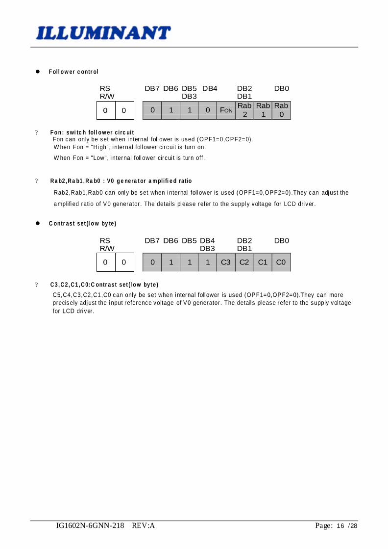
l F oll o w er c ontr ol
RS R/W
0 0
DB7 DB6 DB5 DB4 DB3
DB2 DB1
DB0
? F o n : swi tc h fol l o w er circ ui t
Fon can onl y be set when internal foll ower is used (OPF1=0,OPF2=0). W hen Fon = "High", i nternal foll ower circui t is turn on.
W hen Fon = "Low", i nternal foll ower circui t is turn off. ? Ra b2 , R a b1 , R a b0 : V0 g e nera t or a m plifi e d ratio
Rab2,Rab1,Rab0 can onl y be set when internal foll ower is used (OPF1=0,OPF2=0).They can adjus t the
a mplifi ed rati o of V0 generator . The details please refer to the supply voltage for LCD dri ver .
l C ontr ast set (l o w by te )
RS R/W
0 0
DB7 DB6 DB5 DB4 DB3
DB2 DB1
DB0
? C 3 , C 2 , C 1 , C 0: C ontr ast set (l o w byt e )
C5,C4,C3,C2,C1,C0 can only be set when internal foll ower is used (OPF1=0,OPF2=0).They can more precisely adjust the i nput reference voltage of V0 generator . The detail s please refer to the supply vol tage for LCD dri ver.

IG1602N-6GNN-218 REV:A Page: 17 /28
6.2 Reset Function
Ini tia l izi n g by In ter n al R e s e t Ci rc ui t
An internal reset ci rcuit auto matically i niti alizes the ST7032 when the power is turned on. The foll owing i ns truc ti ons
are executed during the i niti ali zati on. The busy fl ag (BF) is kept i n the busy state (BF = 1) until the i niti alizati on ends.
The busy state l as ts for 40 ms after VD D rises to s table.
1. Display clear
2. Functi on set:
DL = 1; 8-bit i nterface data
N = 0; 1-li ne di splay
DH=0; nor mal 5x8 font
IS=0; use instructi on table 0
3. Display on/off control :
D = 0; Display off
C = 0; Cursor off
B = 0; Bli nking off
4. Entry mode set:
I/D = 1; Increment by 1
S = 0; No shi ft
5. Internal OSC frequency
(F2,F1,F0)=(1,0,0)
6. ICON control
Ion=0; ICO N off
7. Power control BS=0;
1/5bias Bon=0;
booster off Fon=0;
foll ower off
(C5,C4,C3,C2,C1,C0)=(1,0,0,0,0,0)
(Rab2,Rab1,Rab0)=(0,1,0)
Note: If the elec trical characteri sti cs condi ti ons listed under the table Power Supply Conditi ons Using Internal Reset Ci rcuit are not met, the i nternal reset ci rcui t will not operate normally and will fail to i ni ti alize the ST7032. W hen internal Reset Ci rcuit not operate, ST7032 can be reset by XRESET pin fro m MPU control signal .
6.3 Initializing by Instruction
I2C interface(fosc=380k)

IG1602N-6GNN-218 REV:A Page: 11 /28

IG1602N-6GNN-218 REV:A Page: 12 /28
7. IIC Interface Function Description
It just only could write Data or Instruction to ST7032 by the IIC Interface. It could not read Data or Instruction from ST7032 (except Acknowledge signal).
SCL: serial clock input SDA: serial data input Slaver address could only set to 0111110, no other slaver address could be set
The I2C interface send RAM data and executes the commands sent via the I2C Interface. It could send data bit to the RAM.
The I2C Interface is two-line communication between different ICs or modules . The two lines are a Serial Data line (SDA) and a Serial Clock line (SCL). Both lines mus t be connected to a positive supply via a pull-up resis tor. Data trans fer may be initiated only when the bus is not busy.
BIT TRANSFER
One data bit is trans ferred during each clock pulse. The data on the SDA line mus t remain stable during the HIGH period of the clock puls e becaus e changes in the data line at this time will be interpreted as a control signal. Bit transfer is illus trated in Fig.1.
START AND STOP CONDITIONS
Both data and clock lines remain HIGH when the bus is not busy. A HIGH-to-LOW transition of the data line, while the clock is HIGH is defined as the START condition (S). A LOW-to-HIGH transition of the data line while the clock is HIGH is defined as the STOP condition (P). The START and STOP conditions are illus trated in Fig.2.
SYSTEM CONFIGURATION
The system configuration is illus trated in Fig.3. · Transmitter: the device, which sends the data to the bus · Master: the device, which initiates a trans fer, generates clock signals and terminates a trans fer · Slave: the device addressed by a mas ter

IG1602N-6GNN-218 REV:A Page: 13 /28
· Multi-Master: more than one master can attempt to control the bus at the sam e time without corrupting the message · Arbitration: procedure to ensure that, if more than one master simultaneously tries to control the bus, only one is allowed to
do so and the message is not corrupted · Synchronization: procedure to synchronize the clock signals of two or more devices .
ACKNOWLEDGE Acknowledge is not Busy Flag in I2C interface. Each byte of eight bits is followed by an acknowledge bit. The acknowledge bit is a HIGH signal put on the bus by the transmitter during which time the mas ter generates an extra acknowledge related clock pulse. A slave receiver which is addressed mus t generate an acknowledge after the reception of each byte. A master receiver must also generate an acknowledge after the reception of each byte that has been clocked out of the slave transmitter. The device that acknowledges mus t pull-down the SDA line during the acknowledge clock pulse, so that the SDA line is stable LOW during the HIGH period of the acknowledge related clock puls e (set-up and hold times must be taken into consideration). A mas ter receiver mus t signal an end-of-data to the transmitter by not generating an acknowledge on the las t byte that has been clocked out of the slave. In this event the transmitter must leave the data line HIGH to enable the mas ter to generate a STOP condition. Acknowledgement on the I2C Interface is illus trated in Fig.4.
SDA
SCL d at a l i n e
s t abl e ; d at a v al id
c ha n g e of da t a a l lo w ed
Figure 1. Bit transfer
SDA
SCL
S P
S T A R T c on di t i o n S T O P c o n di t i on Figure 2. Definition of START and STOP conditions
MASTER TRANSMITTER
/ RECEIVER
SLAVE RECEIVER (1)0111100
SLAVE RECEIVER (2)0111101
SLAVE RECEIVER (3)0111110
SLAVE RECEIVER (4)0111111
SDA SCL
Figure 3. System configuration

IG1602N-6GNN-218 REV:A Page: 14 /28
I2C Interface protocol The ST7032 supports command, data write addressed slaves on the bus . Before any data is transmitted on the I2C Interface, the device, which should respond, is addressed first. Only one 7-bit slave addresses (0111110) is reserved for the ST7032. The R/W is assigned to 0 for Write only. The I2C Interface protocol is illus trated in Fig.5.
The sequence is initiated with a START condition (S) from the I2C Interface mas ter, which is followed by the slave address. All slaves with the corresponding address acknowledge in parallel, all the others will ignore the I2C Interface transfer. After acknowledgement, one or more command words follow which define the status of the addressed slaves. A command word consis ts of a control byte, which defines Co and RS, plus a data byte. The last control byte is tagged with a cleared mos t significant bit (i.e. the continuation bit Co). After a control byte with a cleared Co bit, only data bytes will follow. The state of the RS bit defines whether the data byte is interpreted as a command or as RAM data. All addressed slaves on the bus also acknowledge the control and data bytes. After the last control byte, depending on the RS bit setting; either a series of display data bytes or command data bytes may follow. If the RS bit is set to logic 1, these display bytes are stored in the display RAM at the address specified by the data pointer. The data pointer is automatically updated and the data is directed to the intended ST7032i device. If the RS bit of the last control byte is set to logic 0, these command bytes will be decoded and the setting of the device will be changed according to the received commands . Only the addressed slave makes the acknowledgement after each byte. At the end of the transmission the I2C INTERFACE-bus mas ter issues a STOP condition (P).

IG1602N-6GNN-218 REV:A Page: 15 /28
8. APPLICATION CIRCUIT 8.1 Timing Characteristics

IG1602N-6GNN-218 REV:A Page: 16 /28
8.2 APPLICATION CIRCUIT

IG1602N-6GNN-218 REV:A Page: 17 /28
9. LCM NUMBERING SYSTEM

IG1602N-6GNN-218 REV:A Page: 18 /28
10. HISTORY
Rev
Date
Item
Page
Comment
1 18/OCT/07 Initial PRELIMINARY
IG1602N-6GNN-218 REV:A Page: 19 /28
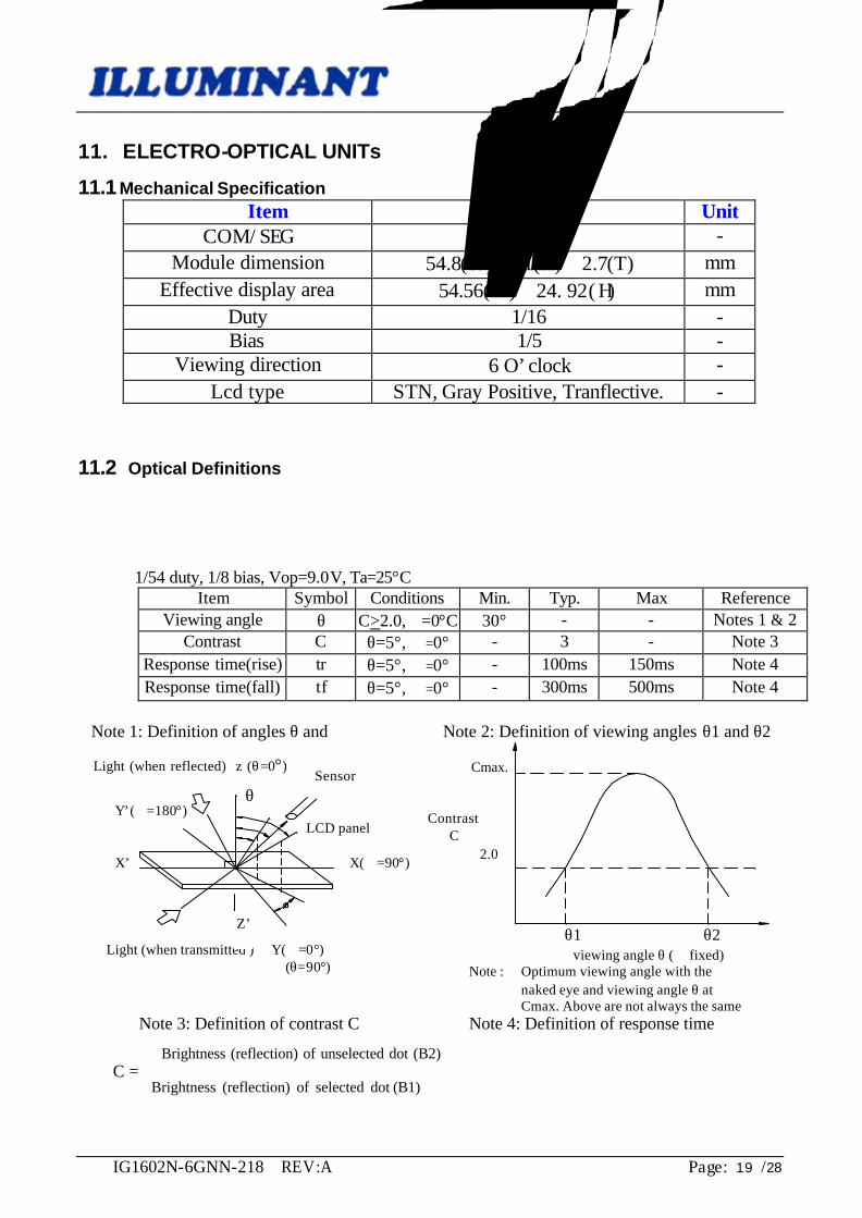
Light (when reflected) z (θ=0°)
11. ELECTRO-OPTICAL UNITs
11.1 Mechanical Specification Item Value Unit COM/SEG 80/16 -
Module dimension 54.8(W)Χ81(H)Χ2.7(T) mm Effective display area 54.56(W)Χ24.92(H) mm
Duty 1/16 - Bias 1/5 -
Viewing direction 6 O’clock - Lcd type STN, Gray Positive, Tranflective. -
11.2 Optical Definitions
1/54 duty, 1/8 bias, Vop=9.0V, Ta=25°C Item Symbol Conditions Min. Typ. Max Reference
Viewing angle θ C>2.0,∅=0°C 30° - - Notes 1 & 2 Contrast C θ=5°, ∅=0° - 3 - Note 3
Response time(rise) tr θ=5°, ∅=0° - 100ms 150ms Note 4 Response time(fall) tf θ=5°, ∅=0° - 300ms 500ms Note 4
Note 1: Definition of angles θ and ∅ Note 2: Definition of viewing angles θ1 and θ2
θ1 θ2
viewing angle θ (∅ fixed) Note : Optimum viewing angle with the naked eye and viewing angle θ at Cmax. Above are not always the same Note 3: Definition of contrast C Note 4: Definition of response time
Brightness (reflection) of unselected dot (B2) C = Brightness (reflection) of selected dot (B1)
Cmax.
Contrast C
2.0
Sensor
LCD panel
X(∅=90°)
Light (when transmitted )
X’
Z’ Y(∅=0°) (θ=90°)
∅
Y’(∅=180°) θ

IG1602N-6GNN-218 REV:A Page: 20 /28
0 Note: Measured with a transmissive LCD operating voltage (v) panel which is displayed 1 cm2
(%)
Brightness (reflection)
Brightness (reflection) of selected dot
Brightness (reflection) of unselected dot B2
B1

IG1602N-6GNN-218 REV:A Page: 21 /28
11.3 Reliability
ITEM Conditions Times (Hrs) OPERATING TEMPERATURE Low Temp. -20 ℃ 240
RANGE TEST High Temp. 70 ℃ 240
STORAGE TEMPERATURE Low Temp. ℃ /
RANGE TEST High Temp. ℃ /
HIGH H U M I D I T Y HIGH Humidity : 90 % R H 240
TEMPERATURE STORAGE Temp. 40 ℃ 240
Humidity : 55~60 % R H 12.5 THERMAL CYCLES
Cycle:10Cycles
11.4 Precautions in Use of LCM
11.4.1 Handing of LCM
¶ Don’t give external shock. ¶ Don’t apply excessive force on the surface. ¶ Liquid in LCD is hazardous substance. Must not lick and swallow. When
the liquid is attach to your hand, skin, cloth etc. Wash it out thoroughly and immediately.
¶ Don’t operate it above the absolute maximum rating. ¶ Don’t disassemble the LCM
11.4.2 Storage ¶ Store in an ambient temperature of 5℃ to 45 ,℃ and in a relative humidity of
40% to 60%. ¶ Don’t expose to sunlight or fluorescent light. ¶ Storage in a clean environment, free from dust, active gas, and solvent. ¶ Store in anti-static electricity container. ¶ Store without any physical load.