if diversity receiver data sheet ad6655 - analog devices · if diversity receiver data sheet ad6655...
TRANSCRIPT
IF Diversity Receiver Data Sheet AD6655
Rev. B Document Feedback Information furnished by Analog Devices is believed to be accurate and reliable. However, no responsibility is assumed by Analog Devices for its use, nor for any infringements of patents or other rights of third parties that may result from its use. Specifications subject to change without notice. No license is granted by implication or otherwise under any patent or patent rights of Analog Devices. Trademarks and registered trademarks are the property of their respective owners.
One Technology Way, P.O. Box 9106, Norwood, MA 02062-9106, U.S.A. Tel: 781.329.4700 ©2007–2014 Analog Devices, Inc. All rights reserved. Technical Support www.analog.com
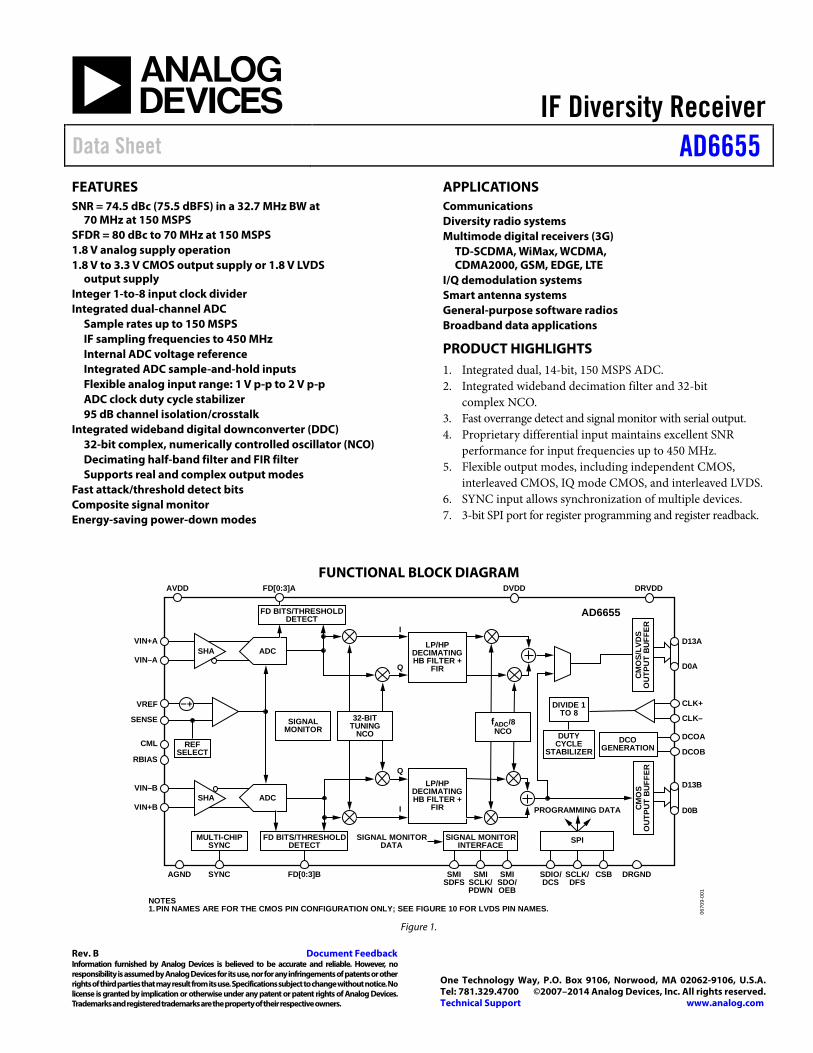
FEATURES SNR = 74.5 dBc (75.5 dBFS) in a 32.7 MHz BW at
70 MHz at 150 MSPS SFDR = 80 dBc to 70 MHz at 150 MSPS 1.8 V analog supply operation 1.8 V to 3.3 V CMOS output supply or 1.8 V LVDS
output supply Integer 1-to-8 input clock divider Integrated dual-channel ADC
Sample rates up to 150 MSPS IF sampling frequencies to 450 MHz Internal ADC voltage reference Integrated ADC sample-and-hold inputs Flexible analog input range: 1 V p-p to 2 V p-p ADC clock duty cycle stabilizer 95 dB channel isolation/crosstalk
Integrated wideband digital downconverter (DDC) 32-bit complex, numerically controlled oscillator (NCO) Decimating half-band filter and FIR filter Supports real and complex output modes
Fast attack/threshold detect bits Composite signal monitor Energy-saving power-down modes
APPLICATIONS Communications Diversity radio systems Multimode digital receivers (3G)
TD-SCDMA, WiMax, WCDMA, CDMA2000, GSM, EDGE, LTE
I/Q demodulation systems Smart antenna systems General-purpose software radios Broadband data applications
PRODUCT HIGHLIGHTS 1. Integrated dual, 14-bit, 150 MSPS ADC. 2. Integrated wideband decimation filter and 32-bit
complex NCO. 3. Fast overrange detect and signal monitor with serial output. 4. Proprietary differential input maintains excellent SNR
performance for input frequencies up to 450 MHz. 5. Flexible output modes, including independent CMOS,
interleaved CMOS, IQ mode CMOS, and interleaved LVDS. 6. SYNC input allows synchronization of multiple devices. 7. 3-bit SPI port for register programming and register readback.
FUNCTIONAL BLOCK DIAGRAM
0670
9-00
1
AVDD FD[0:3]A DVDD DRVDD
AD6655
VIN+A
VIN–A
VREF
SENSE
CML
RBIAS
SHA
SYNC FD[0:3]B SMISDFS
SMISCLK/PDWN
SMISDO/OEB
REFSELECT
ADC
I
Q
Q
I
VIN–B
VIN+B
D13A
D0A
CLK+
CLK–
DCOA
DCOB
D13B
D0BSHA ADC
MULTI-CHIPSYNC
SIGNALMONITOR
DIVIDE 1TO 8
DUTYCYCLE
STABILIZER
AGND
SIGNAL MONITORINTERFACE
CM
OS/
LVD
SO
UTP
UT
BU
FFER
SIGNAL MONITORDATA
SDIO/DCS
SCLK/DFS
CSB DRGND
SPI
PROGRAMMING DATA
FD BITS/THRESHOLDDETECT
FD BITS/THRESHOLDDETECT
32-BITTUNING
NCOfADC/8NCO
LP/HPDECIMATINGHB FILTER +
FIR
LP/HPDECIMATINGHB FILTER +
FIR CM
OS
OU
TPU
T B
UFF
ER
DCOGENERATION
NOTES1.PIN NAMES ARE FOR THE CMOS PIN CONFIGURATION ONLY; SEE FIGURE 10 FOR LVDS PIN NAMES.
Figure 1.

AD6655 Data Sheet
Rev. B | Page 2 of 84
TABLE OF CONTENTS Features .............................................................................................. 1 Applications ....................................................................................... 1 Product Highlights ........................................................................... 1 Functional Block Diagram .............................................................. 1 Revision History ............................................................................... 3 General Description ......................................................................... 4 Specifications ..................................................................................... 5
ADC DC Specifications—AD6655-80/AD6655-105 .............. 5 ADC DC Specifications—AD6655-125/AD6655-150 ............ 6 ADC AC Specifications—AD6655-80/AD6655-105 ............... 7 ADC AC Specifications—AD6655-125/AD6655-150 ............. 8 Digital Specifications—AD6655-80/AD6655-105 ................... 9 Digital Specifications—AD6655-125/AD6655-150 ............... 11 Switching Specifications—AD6655-80/AD6655-105 ............ 13 Switching Specifications—AD6655-125/AD6655-150 ......... 14 Timing Specifications ................................................................ 15
Absolute Maximum Ratings .......................................................... 18 Thermal Characteristics ............................................................ 18 ESD Caution ................................................................................ 18
Pin Configurations and Function Descriptions ......................... 19 Equivalent Circuits ......................................................................... 23 Typical Performance Characteristics ........................................... 24 Theory of Operation ...................................................................... 29
ADC Architecture ...................................................................... 29 Analog Input Considerations .................................................... 29 Voltage Reference ....................................................................... 31 Clock Input Considerations ...................................................... 32 Power Dissipation and Standby Mode ..................................... 34 Digital Outputs ........................................................................... 35
Digital Downconverter .................................................................. 37 Downconverter Modes .............................................................. 37 Numerically Controlled Oscillator (NCO) ............................. 37 Half-Band Decimating Filter and FIR Filter ........................... 37 fADC/8 Fixed-Frequency NCO ................................................... 37
Numerically Controlled Oscillator (NCO) ................................. 38 Frequency Translation ............................................................... 38 NCO Synchronization ............................................................... 38 Phase Offset ................................................................................. 38 NCO Amplitude and Phase Dither .......................................... 38
Decimating Half-Band Filter and FIR filter ................................ 39 Half-Band Filter Coefficients .................................................... 39 Half-Band Filter Features .......................................................... 39 Fixed-Coefficient FIR Filter ...................................................... 39 Synchronization .......................................................................... 40 Combined Filter Performance .................................................. 40 Final NCO ................................................................................... 40
ADC Overrange and Gain Control .............................................. 41 Fast Detect Overview ................................................................. 41 ADC Fast Magnitude ................................................................. 41 ADC Overrange (OR) ................................................................ 42 Gain Switching ............................................................................ 42
Signal Monitor ................................................................................ 44 Peak Detector Mode................................................................... 44 RMS/MS Magnitude Mode ....................................................... 44 Threshold Crossing Mode ......................................................... 45 Additional Control Bits ............................................................. 45 DC Correction ............................................................................ 45 Signal Monitor SPORT Output ................................................ 46
Channel/Chip Synchronization .................................................... 47 Serial Port Interface (SPI) .............................................................. 48
Configuration Using the SPI ..................................................... 48 Hardware Interface ..................................................................... 48 Configuration Without the SPI ................................................ 49 SPI Accessible Features .............................................................. 49
Memory Map .................................................................................. 50 Reading the Memory Map Register Table ............................... 50 Memory Map Register Table ..................................................... 51 Memory Map Register Description ......................................... 55
Applications Information .............................................................. 59 Design Guidelines ...................................................................... 59
Evaluation Board ............................................................................ 61 Power Supplies ............................................................................ 61 Input Signals................................................................................ 61 Output Signals ............................................................................ 61 Default Operation and Jumper Selection Settings ................. 62 Alternative Clock Configurations ............................................ 62 Alternative Analog Input Drive Configuration...................... 63 Schematics ................................................................................... 64

Data Sheet AD6655
Rev. B | Page 3 of 84
Evaluation Board Layouts .......................................................... 74 Bill of Materials ........................................................................... 82
Outline Dimensions ........................................................................ 84
Ordering Guide ........................................................................... 84
REVISION HISTORY 1/14—Rev. A to Rev. B
Removed CP-63-3 Package ............................................... Universal Changes to Address 0x0D, Table 29 .............................................. 52 Changes to Memory Map Description Section ........................... 55 Updated Outline Dimensions ........................................................ 84
9/09—Rev. A to Rev. 0
Added Exposed Pad Notation to Figure 9 and Table 12 ............ 19 Added Exposed Pad Notation to Figure 10 and Table 13 .......... 21 Updated Outline Dimensions ........................................................ 84 Changes to Ordering Guide ........................................................... 85
11/07—Revision 0: Initial Version

AD6655 Data Sheet
Rev. B | Page 4 of 84
GENERAL DESCRIPTION The AD6655 is a mixed-signal intermediate frequency (IF) receiver consisting of dual 14-bit, 80 MSPS/105 MSPS/125 MSPS/150 MSPS ADCs and a wideband digital downconverter (DDC). The AD6655 is designed to support communications applications where low cost, small size, and versatility are desired.
The dual ADC core features a multistage, differential pipelined architecture with integrated output error correction logic. Each ADC features wide bandwidth differential sample-and-hold analog input amplifiers supporting a variety of user-selectable input ranges. An integrated voltage reference eases design consid-erations. A duty cycle stabilizer is provided to compensate for variations in the ADC clock duty cycle, allowing the converters to maintain excellent performance.
ADC data outputs are internally connected directly to the digital downconverter (DDC) of the receiver, simplifying layout and reducing interconnection parasitics. The digital receiver has two channels and provides processing flexibility. Each receive channel has four cascaded signal processing stages: a 32-bit frequency translator (numerically controlled oscillator (NCO)), a half-band decimating filter, a fixed FIR filter, and an fADC/8 fixed-frequency NCO.
In addition to the receiver DDC, the AD6655 has several functions that simplify the automatic gain control (AGC) function in the system receiver. The fast detect feature allows fast overrange detection by outputting four bits of input level information with short latency.
In addition, the programmable threshold detector allows monitoring of the incoming signal power using the four fast detect bits of the ADC with low latency. If the input signal level exceeds the programmable threshold, the coarse upper threshold indicator goes high. Because this threshold indicator has low latency, the user can quickly turn down the system gain to avoid an overrange condition.
The second AGC-related function is the signal monitor. This block allows the user to monitor the composite magnitude of the incoming signal, which aids in setting the gain to optimize the dynamic range of the overall system.
After digital processing, data can be routed directly to the two external 14-bit output ports. These outputs can be set from 1.8 V to 3.3 V CMOS or as 1.8 V LVDS. The CMOS data can also be output in an interleaved configuration at a double data rate using only Port A.
The AD6655 receiver digitizes a wide spectrum of IF frequencies. Each receiver is designed for simultaneous reception of the main channel and the diversity channel. This IF sampling architecture greatly reduces component cost and complexity compared with traditional analog techniques or less integrated digital methods.
Flexible power-down options allow significant power savings, when desired.
Programming for setup and control is accomplished using a 3-bit SPI-compatible serial interface.
The AD6655 is available in a 64-lead LFCSP and is specified over the industrial temperature range of −40°C to +85°C.

Data Sheet AD6655
Rev. B | Page 5 of 84
SPECIFICATIONS ADC DC SPECIFICATIONS—AD6655-80/AD6655-105 AVDD = 1.8 V, DVDD = 1.8 V, DRVDD = 1.8 V, maximum sample rate, VIN = −1.0 dBFS differential input, 1.0 V internal reference, DCS enabled, unless otherwise noted. Table 1.
Parameter AD6655-80 AD6655-105
Unit Temperature Min Typ Max Min Typ Max RESOLUTION Full 14 14 Bits ACCURACY
No Missing Codes Full Guaranteed Guaranteed Offset Error Full ±0.2 ±0.6 ±0.2 ±0.6 % FSR Gain Error Full −3.6 −1.8 −0.1 −4.3 −2.2 −0.5 % FSR
MATCHING CHARACTERISTIC Offset Error 25°C ±0.2 ±0.6 ±0.2 ±0.6 % FSR Gain Error 25°C ±0.2 ±0.75 ±0.2 ±0.75 % FSR
TEMPERATURE DRIFT Offset Error Full ±15 ±15 ppm/°C Gain Error Full ±95 ±95 ppm/°C
INTERNAL VOLTAGE REFERENCE Output Voltage Error (1 V Mode) Full ±5 ±18 ±5 ±18 mV Load Regulation at 1.0 mA Full 7 7 mV
INPUT-REFERRED NOISE VREF = 1.0 V 25°C 0.85 0.85 LSB rms
ANALOG INPUT Input Span, VREF = 1.0 V Full 2 2 V p-p Input Capacitance1 Full 8 8 pF
VREF INPUT RESISTANCE Full 6 6 kΩ POWER SUPPLIES
Supply Voltage AVDD, DVDD Full 1.7 1.8 1.9 1.7 1.8 1.9 V DRVDD (CMOS Mode) Full 1.7 3.3 3.6 1.7 3.3 3.6 V DRVDD (LVDS Mode) Full 1.7 1.8 1.9 1.7 1.8 1.9 V
Supply Current IAVDD
2, 3 Full 235 420 315 575 mA
IDVDD2, 3 Full 175 225 mA
IDRVDD2 (3.3 V CMOS) Full 18 21 mA
IDRVDD2 (1.8 V CMOS) Full 8 11 mA
IDRVDD2 (1.8 V LVDS) Full 55 56 mA
POWER CONSUMPTION DC Input Full 470 490 620 650 mW Sine Wave Input2 (DRVDD = 1.8 V) Full 755 995 mW Sine Wave Input2 (DRVDD = 3.3 V) Full 800 1040 mW Standby Power4 Full 52 68 mW Power-Down Power Full 2.5 8 2.5 8 mW
1 Input capacitance refers to the effective capacitance between one differential input pin and AGND. See Figure 11 for the equivalent analog input structure. 2 Measured with a 9.7 MHz, full-scale sine wave input, NCO enabled with a frequency of 13 MHz, FIR filter enabled and the fS/8 output mix enabled with approximately
5 pF loading on each output bit. 3 The maximum limit applies to the combination of IAVDD and IDVDD currents. 4 Standby power is measured with a dc input and with the CLK pin inactive (set to AVDD or AGND).
AD6655 Data Sheet
Rev. B | Page 6 of 84
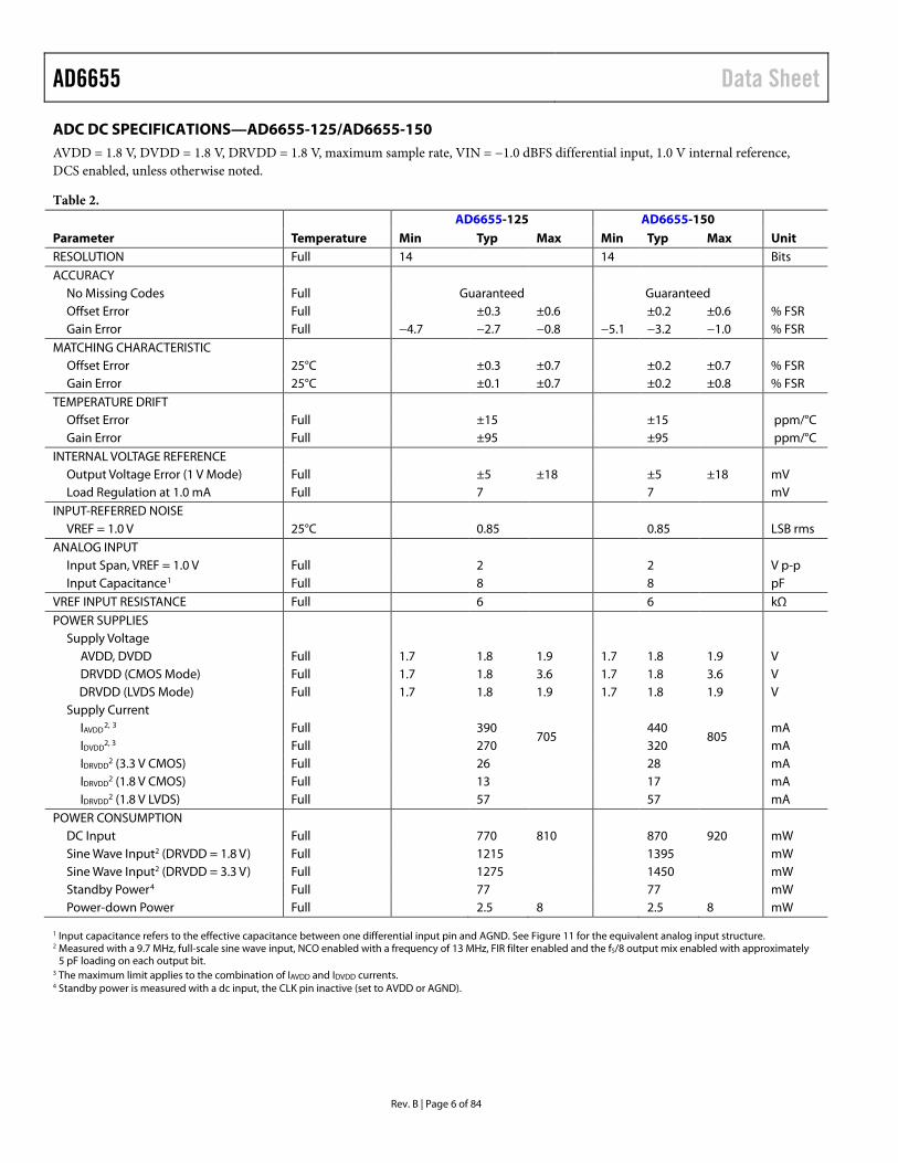
ADC DC SPECIFICATIONS—AD6655-125/AD6655-150 AVDD = 1.8 V, DVDD = 1.8 V, DRVDD = 1.8 V, maximum sample rate, VIN = −1.0 dBFS differential input, 1.0 V internal reference, DCS enabled, unless otherwise noted.
Table 2.
Parameter Temperature
AD6655-125 AD6655-150
Unit Min Typ Max Min Typ Max RESOLUTION Full 14 14 Bits ACCURACY
No Missing Codes Full Guaranteed Guaranteed Offset Error Full ±0.3 ±0.6 ±0.2 ±0.6 % FSR Gain Error Full −4.7 −2.7 −0.8 −5.1 −3.2 −1.0 % FSR
MATCHING CHARACTERISTIC Offset Error 25°C ±0.3 ±0.7 ±0.2 ±0.7 % FSR Gain Error 25°C ±0.1 ±0.7 ±0.2 ±0.8 % FSR
TEMPERATURE DRIFT Offset Error Full ±15 ±15 ppm/°C Gain Error Full ±95 ±95 ppm/°C
INTERNAL VOLTAGE REFERENCE Output Voltage Error (1 V Mode) Full ±5 ±18 ±5 ±18 mV Load Regulation at 1.0 mA Full 7 7 mV
INPUT-REFERRED NOISE VREF = 1.0 V 25°C 0.85 0.85 LSB rms
ANALOG INPUT Input Span, VREF = 1.0 V Full 2 2 V p-p Input Capacitance1 Full 8 8 pF
VREF INPUT RESISTANCE Full 6 6 kΩ POWER SUPPLIES
Supply Voltage AVDD, DVDD Full 1.7 1.8 1.9 1.7 1.8 1.9 V DRVDD (CMOS Mode) Full 1.7 1.8 3.6 1.7 1.8 3.6 V DRVDD (LVDS Mode) Full 1.7 1.8 1.9 1.7 1.8 1.9 V
Supply Current IAVDD
2, 3 Full 390 705
440 805
mA IDVDD
2, 3 Full 270 320 mA IDRVDD
2 (3.3 V CMOS) Full 26 28 mA IDRVDD
2 (1.8 V CMOS) Full 13 17 mA IDRVDD
2 (1.8 V LVDS) Full 57 57 mA POWER CONSUMPTION
DC Input Full 770 810 870 920 mW Sine Wave Input2 (DRVDD = 1.8 V) Full 1215 1395 mW Sine Wave Input2 (DRVDD = 3.3 V) Full 1275 1450 mW Standby Power4 Full 77 77 mW Power-down Power Full 2.5 8 2.5 8 mW
1 Input capacitance refers to the effective capacitance between one differential input pin and AGND. See Figure 11 for the equivalent analog input structure. 2 Measured with a 9.7 MHz, full-scale sine wave input, NCO enabled with a frequency of 13 MHz, FIR filter enabled and the fS/8 output mix enabled with approximately
5 pF loading on each output bit. 3 The maximum limit applies to the combination of IAVDD and IDVDD currents. 4 Standby power is measured with a dc input, the CLK pin inactive (set to AVDD or AGND).

Data Sheet AD6655
Rev. B | Page 7 of 84
ADC AC SPECIFICATIONS—AD6655-80/AD6655-105 AVDD = 1.8 V, DVDD = 1.8 V, DRVDD = 1.8 V, maximum sample rate, VIN = −1.0 dBFS differential input, 1.0 V internal reference, DCS enabled, NCO enabled, half-band filter enabled, FIR filter enabled, unless otherwise noted.
Table 3.
Parameter1 Temperature AD6655-80 AD6655-105
Unit Min Typ Max Min Typ Max SIGNAL-TO-NOISE-RATIO (SNR)
fIN = 2.4 MHz 25°C 74.9 74.8 dB fIN = 70 MHz 25°C 74.8 74.7 dB Full 73.0 73.0 dB fIN = 140 MHz 25°C 74.5 74.3 dB fIN = 220 MHz 25°C 73.4 73.4 dB
WORST SECOND OR THIRD HARMONIC fIN = 2.4 MHz 25°C −86 −86 dBc
fIN = 70 MHz 25°C −85 −85 dBc
Full −74 −74 dBc
fIN = 140 MHz 25°C −84 −84 dBc
fIN = 220 MHz 25°C −83 −83 dBc
SPURIOUS-FREE DYNAMIC RANGE (SFDR)
fIN = 2.4 MHz 25°C 86 86 dBc
fIN = 70 MHz 25°C 85 85 dBc
Full 74 74 dBc
fIN = 140 MHz 25°C 84 84 dBc
fIN = 220 MHz 25°C 83 83 dBc
WORST OTHER HARMONIC OR SPUR2
fIN = 2.4 MHz 25°C −93 −93 dBc
fIN = 70 MHz 25°C −90 −90 dBc
Full −82 −82 dBc
fIN = 140 MHz 25°C −89 −89 dBc
fIN = 220 MHz 25°C −86 −86 dBc
TWO-TONE SFDR
fIN = 29.12 MHz, 32.12 MHz (−7 dBFS) 25°C 85 85 dBc
fIN = 169.12 MHz, 172.12 MHz (−7 dBFS) 25°C 81 81 dBc
CROSSTALK3 Full 95 95 dB
ANALOG INPUT BANDWIDTH 25°C 650 650 MHz 1 See Application Note AN-835, Understanding High Speed ADC Testing and Evaluation, for a complete set of definitions. 2 See the Applications Information section for more information about the worst other specifications for the AD6655. 3 Crosstalk is measured at 100 MHz with −1 dBFS on one channel and with no input on the alternate channel.
AD6655 Data Sheet
Rev. B | Page 8 of 84
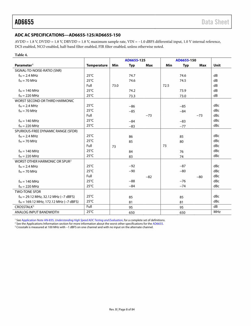
ADC AC SPECIFICATIONS—AD6655-125/AD6655-150 AVDD = 1.8 V, DVDD = 1.8 V, DRVDD = 1.8 V, maximum sample rate, VIN = −1.0 dBFS differential input, 1.0 V internal reference, DCS enabled, NCO enabled, half-band filter enabled, FIR filter enabled, unless otherwise noted.
Table 4.
Parameter1 Temperature AD6655-125 AD6655-150
Unit Min Typ Max Min Typ Max SIGNAL-TO-NOISE-RATIO (SNR)
fIN = 2.4 MHz 25°C 74.7 74.6 dB fIN = 70 MHz 25°C 74.6 74.5 dB Full 73.0 72.5 dB fIN = 140 MHz 25°C 74.2 73.9 dB fIN = 220 MHz 25°C 73.3 73.0 dB
WORST SECOND OR THIRD HARMONIC fIN = 2.4 MHz 25°C −86 −85 dBc
fIN = 70 MHz 25°C −85 −84 dBc
Full −73 −73 dBc
fIN = 140 MHz 25°C −84 −83 dBc
fIN = 220 MHz 25°C −83 −77 dBc
SPURIOUS-FREE DYNAMIC RANGE (SFDR)
fIN = 2.4 MHz 25°C 86 85 dBc
fIN = 70 MHz 25°C 85 80 dBc
Full 73 73 dBc
fIN = 140 MHz 25°C 84 76 dBc
fIN = 220 MHz 25°C 83 74 dBc
WORST OTHER HARMONIC OR SPUR2
fIN = 2.4 MHz 25°C −92 −87 dBc
fIN = 70 MHz 25°C −90 −80 dBc
Full −82 −80 dBc
fIN = 140 MHz 25°C −88 −76 dBc
fIN = 220 MHz 25°C −84 −74 dBc
TWO-TONE SFDR
fIN = 29.12 MHz, 32.12 MHz (−7 dBFS) 25°C 85 85 dBc
fIN = 169.12 MHz, 172.12 MHz (−7 dBFS) 25°C 81 81 dBc
CROSSTALK3 Full 95 95 dB
ANALOG INPUT BANDWIDTH 25°C 650 650 MHz 1 See Application Note AN-835, Understanding High Speed ADC Testing and Evaluation, for a complete set of definitions. 2 See the Applications Information section for more information about the worst other specifications for the AD6655. 3 Crosstalk is measured at 100 MHz with −1 dBFS on one channel and with no input on the alternate channel.
Data Sheet AD6655
Rev. B | Page 9 of 84
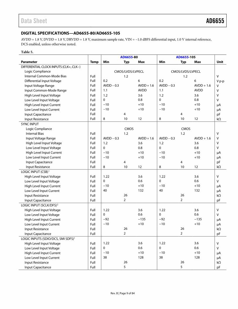
DIGITAL SPECIFICATIONS—AD6655-80/AD6655-105 AVDD = 1.8 V, DVDD = 1.8 V, DRVDD = 1.8 V, maximum sample rate, VIN = −1.0 dBFS differential input, 1.0 V internal reference, DCS enabled, unless otherwise noted.
Table 5.
Parameter Temp AD6655-80 AD6655-105
Unit Min Typ Max Min Typ Max DIFFERENTIAL CLOCK INPUTS (CLK+, CLK−)
Logic Compliance CMOS/LVDS/LVPECL CMOS/LVDS/LVPECL Internal Common-Mode Bias Full 1.2 1.2 V Differential Input Voltage Full 0.2 6 0.2 6 V p-p Input Voltage Range Full AVDD − 0.3 AVDD + 1.6 AVDD − 0.3 AVDD + 1.6 V Input Common-Mode Range Full 1.1 AVDD 1.1 AVDD V High Level Input Voltage Full 1.2 3.6 1.2 3.6 V Low Level Input Voltage Full 0 0.8 0 0.8 V High Level Input Current Full −10 +10 −10 +10 µA Low Level Input Current Full −10 +10 −10 +10 µA Input Capacitance Full 4 4 pF Input Resistance Full 8 10 12 8 10 12 kΩ
SYNC INPUT Logic Compliance CMOS CMOS Internal Bias Full 1.2 1.2 V Input Voltage Range Full AVDD − 0.3 AVDD + 1.6 AVDD − 0.3 AVDD + 1.6 V High Level Input Voltage Full 1.2 3.6 1.2 3.6 V Low Level Input Voltage Full 0 0.8 0 0.8 V High Level Input Current Full −10 +10 −10 +10 µA Low Level Input Current Full −10 +10 −10 +10 µA Input Capacitance Full 4 4 pF Input Resistance Full 8 10 12 8 10 12 kΩ
LOGIC INPUT (CSB)1 High Level Input Voltage Full 1.22 3.6 1.22 3.6 V Low Level Input Voltage Full 0 0.6 0 0.6 V High Level Input Current Full −10 +10 −10 +10 µA Low Level Input Current Full 40 132 40 132 µA Input Resistance Full 26 26 kΩ Input Capacitance Full 2 2 pF
LOGIC INPUT (SCLK/DFS)2 High Level Input Voltage Full 1.22 3.6 1.22 3.6 V Low Level Input Voltage Full 0 0.6 0 0.6 V High Level Input Current Full −92 −135 −92 −135 µA Low Level Input Current Full −10 +10 −10 +10 µA Input Resistance Full 26 26 kΩ Input Capacitance Full 2 2 pF
LOGIC INPUTS (SDIO/DCS, SMI SDFS)1 High Level Input Voltage Full 1.22 3.6 1.22 3.6 V Low Level Input Voltage Full 0 0.6 0 0.6 V High Level Input Current Full −10 +10 −10 +10 µA Low Level Input Current Full 38 128 38 128 µA Input Resistance Full 26 26 kΩ Input Capacitance Full 5 5 pF
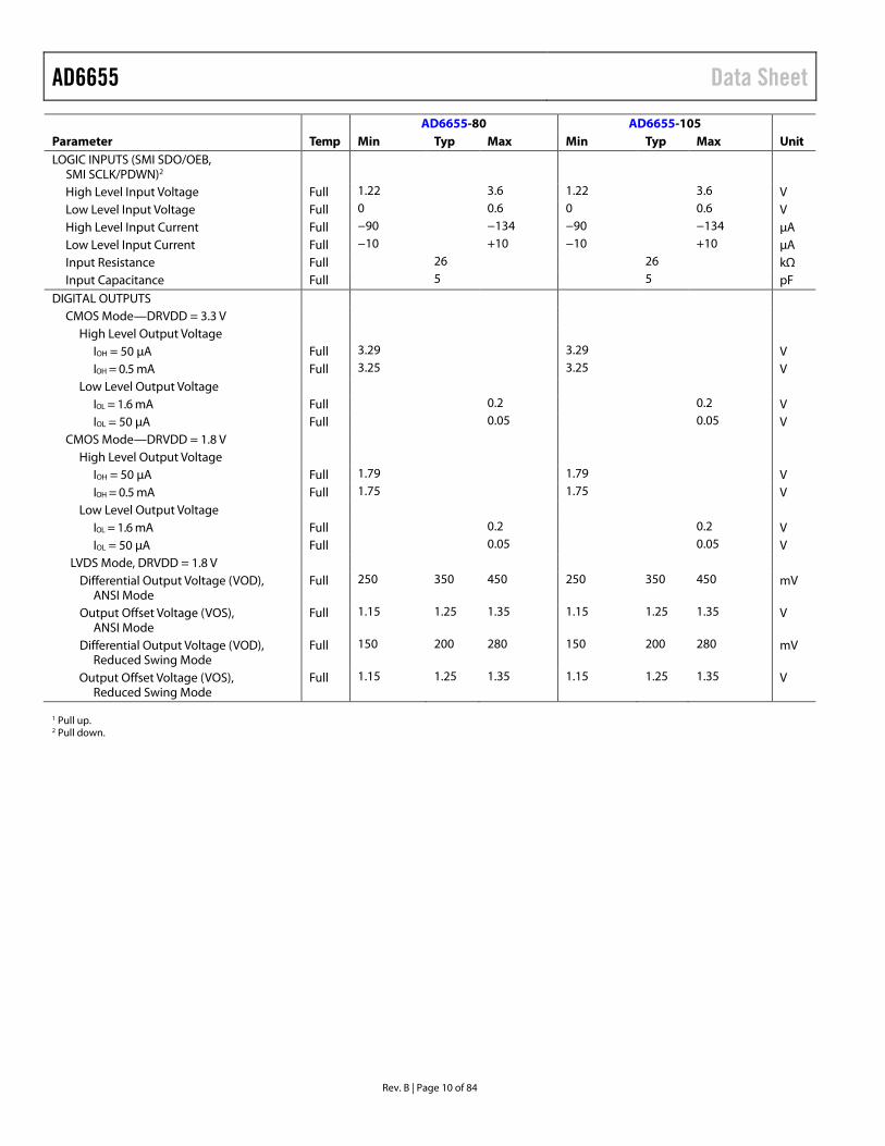
AD6655 Data Sheet
Rev. B | Page 10 of 84
Parameter Temp AD6655-80 AD6655-105
Unit Min Typ Max Min Typ Max LOGIC INPUTS (SMI SDO/OEB,
SMI SCLK/PDWN)2
High Level Input Voltage Full 1.22 3.6 1.22 3.6 V Low Level Input Voltage Full 0 0.6 0 0.6 V High Level Input Current Full −90 −134 −90 −134 µA Low Level Input Current Full −10 +10 −10 +10 µA Input Resistance Full 26 26 kΩ Input Capacitance Full 5 5 pF
DIGITAL OUTPUTS CMOS Mode—DRVDD = 3.3 V
High Level Output Voltage IOH = 50 µA Full 3.29 3.29 V IOH = 0.5 mA Full 3.25 3.25 V
Low Level Output Voltage IOL = 1.6 mA Full 0.2 0.2 V IOL = 50 µA Full 0.05 0.05 V
CMOS Mode—DRVDD = 1.8 V High Level Output Voltage
IOH = 50 µA Full 1.79 1.79 V IOH = 0.5 mA Full 1.75 1.75 V
Low Level Output Voltage IOL = 1.6 mA Full 0.2 0.2 V IOL = 50 µA Full 0.05 0.05 V
LVDS Mode, DRVDD = 1.8 V Differential Output Voltage (VOD),
ANSI Mode Full 250 350 450 250 350 450 mV
Output Offset Voltage (VOS), ANSI Mode
Full 1.15 1.25 1.35 1.15 1.25 1.35 V
Differential Output Voltage (VOD), Reduced Swing Mode
Full 150 200 280 150 200 280 mV
Output Offset Voltage (VOS), Reduced Swing Mode
Full 1.15 1.25 1.35 1.15 1.25 1.35 V
1 Pull up. 2 Pull down.

Data Sheet AD6655
Rev. B | Page 11 of 84
DIGITAL SPECIFICATIONS—AD6655-125/AD6655-150 AVDD = 1.8 V, DVDD = 1.8 V, DRVDD = 1.8 V, maximum sample rate, VIN = −1.0 dBFS differential input, 1.0 V internal reference, DCS enabled, unless otherwise noted.
Table 6.
Parameter Temp AD6655-125 AD6655-150
Unit Min Typ Max Min Typ Max DIFFERENTIAL CLOCK INPUTS (CLK+, CLK−)
Logic Compliance CMOS/LVDS/LVPECL CMOS/LVDS/LVPECL Internal Common-Mode Bias Full 1.2 1.2 V Differential Input Voltage Full 0.2 6 0.2 6 V p-p Input Voltage Range Full AVDD − 0.3 AVDD + 1.6 AVDD − 0.3 AVDD + 1.6 V Input Common-Mode Range Full 1.1 V AVDD 1.1 V AVDD V High Level Input Voltage Full 1.2 3.6 1.2 3.6 V Low Level Input Voltage Full 0 0.8 0 0.8 V High Level Input Current Full −10 +10 −10 +10 µA Low Level Input Current Full −10 +10 −10 +10 µA Input Capacitance Full 4 4 pF Input Resistance Full 8 10 12 8 10 12 kΩ
SYNC INPUT Logic Compliance CMOS CMOS Internal Bias Full 1.2 1.2 V Input Voltage Range Full AVDD − 0.3 AVDD + 1.6 AVDD − 0.3 AVDD + 1.6 V High Level Input Voltage Full 1.2 3.6 1.2 3.6 V Low Level Input Voltage Full 0 0.8 0 0.8 V High Level Input Current Full −10 +10 −10 +10 µA Low Level Input Current Full −10 +10 −10 +10 µA Input Capacitance Full 4 4 pF Input Resistance Full 8 10 12 8 10 12 kΩ
LOGIC INPUT (CSB)1 High Level Input Voltage Full 1.22 3.6 1.22 3.6 V Low Level Input Voltage Full 0 0.6 0 0.6 V High Level Input Current Full −10 +10 −10 +10 µA Low Level Input Current Full 40 132 40 132 µA Input Resistance Full 26 26 kΩ Input Capacitance Full 2 2 pF
LOGIC INPUT (SCLK/DFS)2 High Level Input Voltage Full 1.22 3.6 1.22 3.6 V Low Level Input Voltage Full 0 0.6 0 0.6 V High Level Input Current Full −92 −135 −92 −135 µA Low Level Input Current Full −10 +10 −10 +10 µA Input Resistance Full 26 26 kΩ Input Capacitance Full 2 2 pF
LOGIC INPUTS (SDIO/DCS, SMI SDFS)1 High Level Input Voltage Full 1.22 3.6 1.22 3.6 V Low Level Input Voltage Full 0 0.6 0 0.6 V High Level Input Current Full −10 +10 −10 +10 µA Low Level Input Current Full 38 128 38 128 µA Input Resistance Full 26 26 kΩ Input Capacitance Full 5 5 pF
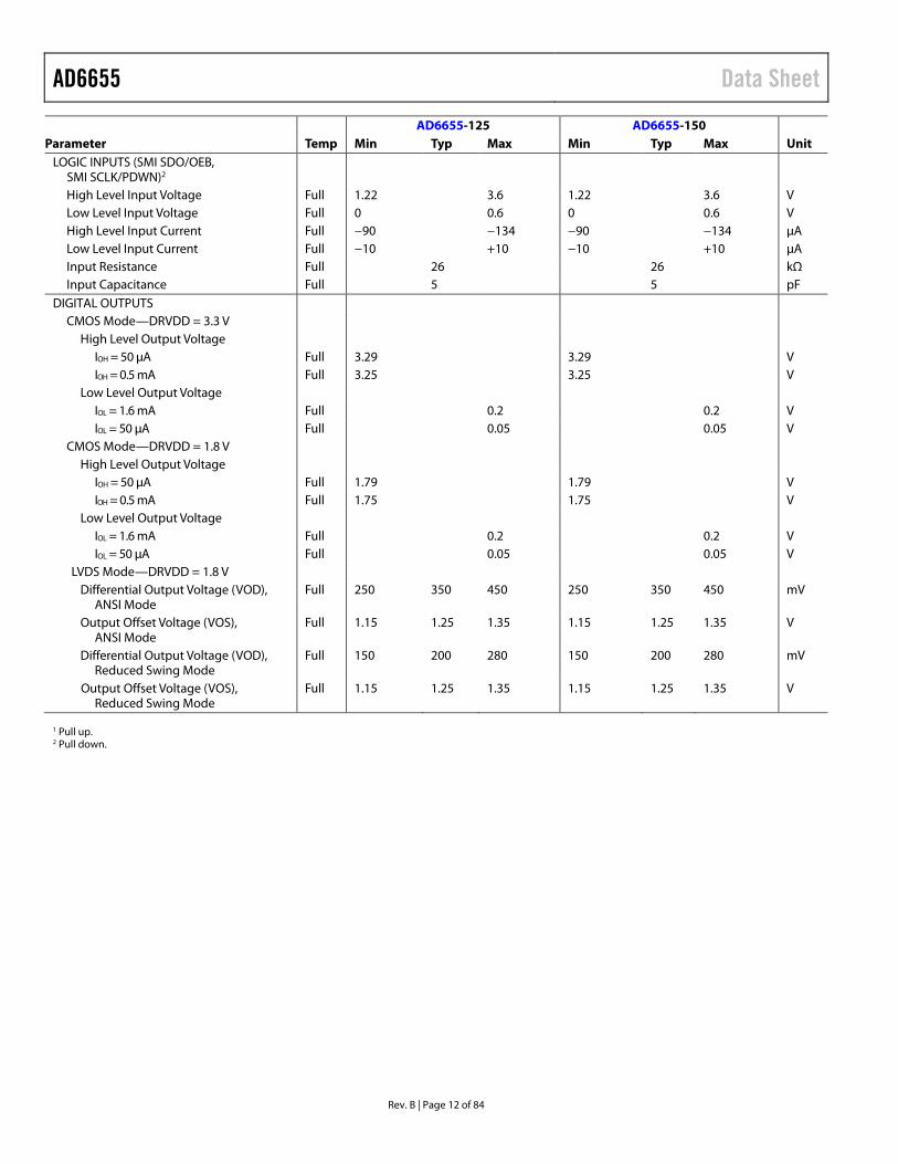
AD6655 Data Sheet
Rev. B | Page 12 of 84
Parameter Temp AD6655-125 AD6655-150
Unit Min Typ Max Min Typ Max LOGIC INPUTS (SMI SDO/OEB,
SMI SCLK/PDWN)2
High Level Input Voltage Full 1.22 3.6 1.22 3.6 V Low Level Input Voltage Full 0 0.6 0 0.6 V High Level Input Current Full −90 −134 −90 −134 µA Low Level Input Current Full −10 +10 −10 +10 µA Input Resistance Full 26 26 kΩ Input Capacitance Full 5 5 pF
DIGITAL OUTPUTS CMOS Mode—DRVDD = 3.3 V
High Level Output Voltage IOH = 50 µA Full 3.29 3.29 V IOH = 0.5 mA Full 3.25 3.25 V
Low Level Output Voltage IOL = 1.6 mA Full 0.2 0.2 V IOL = 50 µA Full 0.05 0.05 V
CMOS Mode—DRVDD = 1.8 V High Level Output Voltage
IOH = 50 µA Full 1.79 1.79 V IOH = 0.5 mA Full 1.75 1.75 V
Low Level Output Voltage IOL = 1.6 mA Full 0.2 0.2 V IOL = 50 µA Full 0.05 0.05 V
LVDS Mode—DRVDD = 1.8 V Differential Output Voltage (VOD),
ANSI Mode Full 250 350 450 250 350 450 mV
Output Offset Voltage (VOS), ANSI Mode
Full 1.15 1.25 1.35 1.15 1.25 1.35 V
Differential Output Voltage (VOD), Reduced Swing Mode
Full 150 200 280 150 200 280 mV
Output Offset Voltage (VOS), Reduced Swing Mode
Full 1.15 1.25 1.35 1.15 1.25 1.35 V
1 Pull up. 2 Pull down.
Data Sheet AD6655
Rev. B | Page 13 of 84
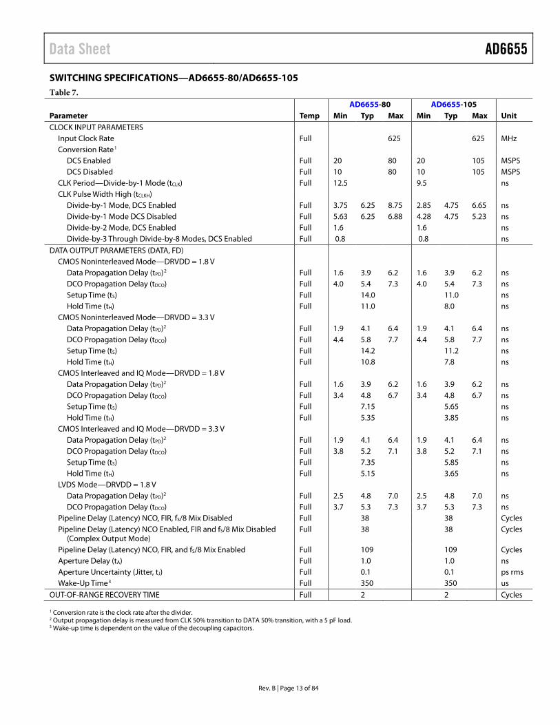
SWITCHING SPECIFICATIONS—AD6655-80/AD6655-105 Table 7.
Parameter Temp AD6655-80 AD6655-105
Unit Min Typ Max Min Typ Max CLOCK INPUT PARAMETERS
Input Clock Rate Full 625 625 MHz Conversion Rate1
DCS Enabled Full 20 80 20 105 MSPS DCS Disabled Full 10 80 10 105 MSPS
CLK Period—Divide-by-1 Mode (tCLK) Full 12.5 9.5 ns CLK Pulse Width High (tCLKH)
Divide-by-1 Mode, DCS Enabled Full 3.75 6.25 8.75 2.85 4.75 6.65 ns Divide-by-1 Mode DCS Disabled Full 5.63 6.25 6.88 4.28 4.75 5.23 ns Divide-by-2 Mode, DCS Enabled Full 1.6 1.6 ns Divide-by-3 Through Divide-by-8 Modes, DCS Enabled Full 0.8 0.8 ns
DATA OUTPUT PARAMETERS (DATA, FD) CMOS Noninterleaved Mode—DRVDD = 1.8 V
Data Propagation Delay (tPD)2 Full 1.6 3.9 6.2 1.6 3.9 6.2 ns DCO Propagation Delay (tDCO) Full 4.0 5.4 7.3 4.0 5.4 7.3 ns Setup Time (tS) Full 14.0 11.0 ns Hold Time (tH) Full 11.0 8.0 ns
CMOS Noninterleaved Mode—DRVDD = 3.3 V Data Propagation Delay (tPD)2 Full 1.9 4.1 6.4 1.9 4.1 6.4 ns DCO Propagation Delay (tDCO) Full 4.4 5.8 7.7 4.4 5.8 7.7 ns Setup Time (tS) Full 14.2 11.2 ns Hold Time (tH) Full 10.8 7.8 ns
CMOS Interleaved and IQ Mode—DRVDD = 1.8 V Data Propagation Delay (tPD)2 Full 1.6 3.9 6.2 1.6 3.9 6.2 ns DCO Propagation Delay (tDCO) Full 3.4 4.8 6.7 3.4 4.8 6.7 ns Setup Time (tS) Full 7.15 5.65 ns Hold Time (tH) Full 5.35 3.85 ns
CMOS Interleaved and IQ Mode—DRVDD = 3.3 V Data Propagation Delay (tPD)2 Full 1.9 4.1 6.4 1.9 4.1 6.4 ns DCO Propagation Delay (tDCO) Full 3.8 5.2 7.1 3.8 5.2 7.1 ns Setup Time (tS) Full 7.35 5.85 ns Hold Time (tH) Full 5.15 3.65 ns
LVDS Mode—DRVDD = 1.8 V Data Propagation Delay (tPD)2 Full 2.5 4.8 7.0 2.5 4.8 7.0 ns DCO Propagation Delay (tDCO) Full 3.7 5.3 7.3 3.7 5.3 7.3 ns
Pipeline Delay (Latency) NCO, FIR, fS/8 Mix Disabled Full 38 38 Cycles Pipeline Delay (Latency) NCO Enabled, FIR and fS/8 Mix Disabled
(Complex Output Mode) Full 38 38 Cycles
Pipeline Delay (Latency) NCO, FIR, and fS/8 Mix Enabled Full 109 109 Cycles Aperture Delay (tA) Full 1.0 1.0 ns Aperture Uncertainty (Jitter, tJ) Full 0.1 0.1 ps rms Wake-Up Time3 Full 350 350 us
OUT-OF-RANGE RECOVERY TIME Full 2 2 Cycles 1 Conversion rate is the clock rate after the divider. 2 Output propagation delay is measured from CLK 50% transition to DATA 50% transition, with a 5 pF load. 3 Wake-up time is dependent on the value of the decoupling capacitors.

AD6655 Data Sheet
Rev. B | Page 14 of 84
SWITCHING SPECIFICATIONS—AD6655-125/AD6655-150 Table 8.
Parameter Temp AD6655-125 AD6655-150
Unit Min Typ Max Min Typ Max CLOCK INPUT PARAMETERS
Input Clock Rate Full 625 625 MHz Conversion Rate1
DCS Enabled Full 20 125 20 150 MSPS DCS Disabled Full 10 125 10 150 MSPS
CLK Period—Divide-by-1 Mode (tCLK) Full 8 6.66 ns CLK Pulse Width High (tCLKH)
Divide-by-1 Mode, DCS Enabled Full 2.4 4 5.6 2.0 3.33 4.66 ns Divide-by-1 Mode, DCS Disabled Full 3.6 4 4.4 3.0 3.33 3.66 ns Divide-by-2 Mode, DCS Enabled Full 1.6 1.6 ns Divide-by-3 Through Divide-by-8 Modes, DCS Enabled Full 0.8 0.8 ns
DATA OUTPUT PARAMETERS (DATA, FD) CMOS Noninterleaved Mode—DRVDD = 1.8 V
Data Propagation Delay (tPD)2 Full 1.6 3.9 6.2 1.6 3.9 6.2 ns DCO Propagation Delay (tDCO) Full 4.0 5.4 7.3 4.0 5.4 7.3 ns Setup Time (tS) Full 9.5 8.16 ns Hold Time (tH) Full 6.5 5.16 ns
CMOS Noninterleaved Mode—DRVDD = 3.3 V Data Propagation Delay (tPD)2 Full 1.9 4.1 6.4 1.9 4.1 6.4 ns DCO Propagation Delay (tDCO) Full 4.4 5.8 7.7 4.4 5.8 7.7 ns Setup Time (tS) Full 9.7 8.36 ns Hold Time (tH) Full 6.3 4.96 ns
CMOS Interleaved and IQ Mode—DRVDD = 1.8 V Data Propagation Delay (tPD)2 Full 1.6 3.9 6.2 1.6 3.9 6.2 ns DCO Propagation Delay (tDCO) Full 3.4 4.8 6.7 3.4 4.8 6.7 ns Setup Time (tS) Full 4.9 4.23 ns Hold Time (tH) Full 3.1 2.43 ns
CMOS Interleaved and IQ Mode—DRVDD = 3.3 V Data Propagation Delay (tPD)2 Full 1.9 4.1 6.4 1.9 4.1 6.4 ns DCO Propagation Delay (tDCO) Full 3.8 5.2 7.1 3.8 5.2 7.1 ns Setup Time (tS) Full 5.1 4.43 ns Hold Time (tH) Full 2.9 2.23 ns
LVDS Mode—DRVDD = 1.8 V Data Propagation Delay (tPD)2 Full 2.5 4.8 7.0 2.5 4.8 7.0 ns DCO Propagation Delay (tDCO) Full 3.7 5.3 7.3 3.7 5.3 7.3 ns
Pipeline Delay (Latency) NCO, FIR, fS/8 Mix Disabled Full 38 38 Cycles Pipeline Delay (Latency) NCO Enabled; FIR and fS/8 Mix Disabled
(Complex Output Mode) Full 38 38 Cycles
Pipeline Delay (Latency) NCO, FIR, and fS/8 Mix Enabled Full 109 109 Cycles Aperture Delay (tA) Full 1.0 1.0 ns Aperture Uncertainty (Jitter, tJ) Full 0.1 0.1 ps rms Wake-Up Time3 Full 350 350 us
OUT-OF-RANGE RECOVERY TIME Full 3 3 Cycles 1 Conversion rate is the clock rate after the divider. 2 Output propagation delay is measured from CLK 50% transition to DATA 50% transition, with a 5 pF load. 3 Wake-up time is dependent on the value of the decoupling capacitors.
Data Sheet AD6655
Rev. B | Page 15 of 84
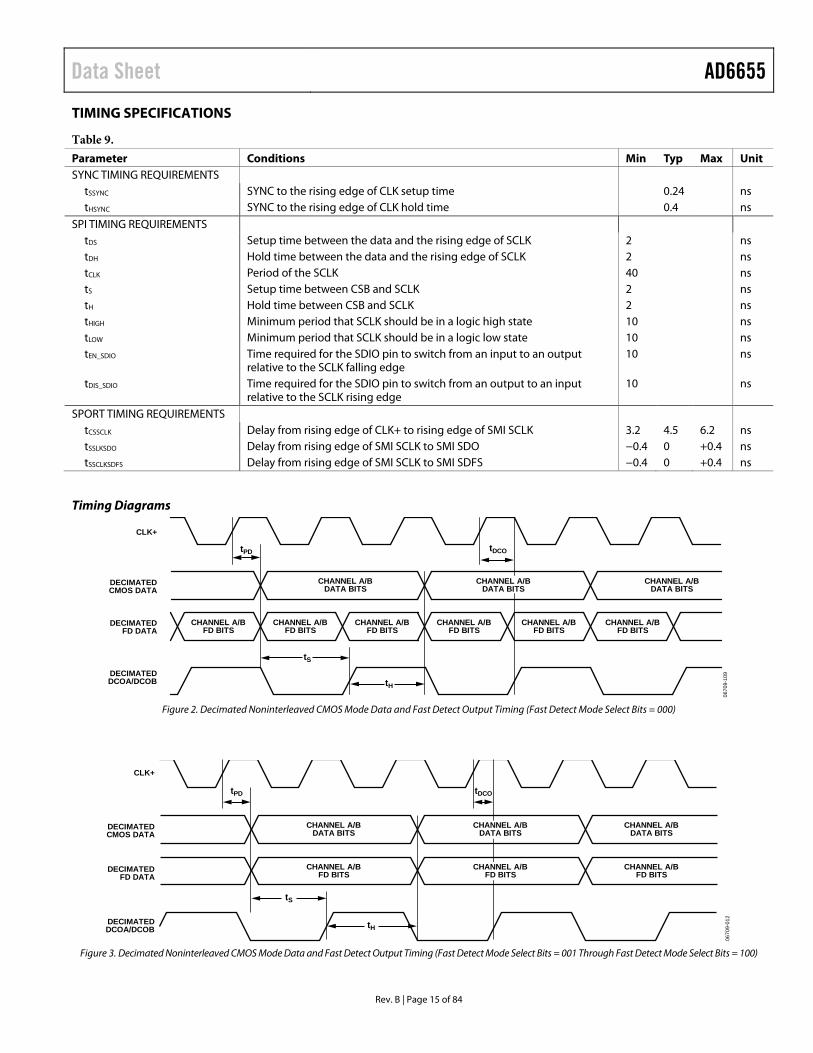
TIMING SPECIFICATIONS
Table 9. Parameter Conditions Min Typ Max Unit SYNC TIMING REQUIREMENTS
tSSYNC SYNC to the rising edge of CLK setup time 0.24 ns tHSYNC SYNC to the rising edge of CLK hold time 0.4 ns
SPI TIMING REQUIREMENTS tDS Setup time between the data and the rising edge of SCLK 2 ns tDH Hold time between the data and the rising edge of SCLK 2 ns tCLK Period of the SCLK 40 ns tS Setup time between CSB and SCLK 2 ns tH Hold time between CSB and SCLK 2 ns tHIGH Minimum period that SCLK should be in a logic high state 10 ns tLOW Minimum period that SCLK should be in a logic low state 10 ns tEN_SDIO Time required for the SDIO pin to switch from an input to an output
relative to the SCLK falling edge 10 ns
tDIS_SDIO Time required for the SDIO pin to switch from an output to an input relative to the SCLK rising edge
10 ns
SPORT TIMING REQUIREMENTS tCSSCLK Delay from rising edge of CLK+ to rising edge of SMI SCLK 3.2 4.5 6.2 ns tSSLKSDO Delay from rising edge of SMI SCLK to SMI SDO −0.4 0 +0.4 ns tSSCLKSDFS Delay from rising edge of SMI SCLK to SMI SDFS −0.4 0 +0.4 ns
Timing Diagrams
0670
9-10
9
tH
tS
CLK+
DECIMATEDCMOS DATA
DECIMATEDFD DATA
CHANNEL A/BFD BITS
CHANNEL A/BFD BITS
CHANNEL A/BFD BITS
CHANNEL A/BDATA BITS
CHANNEL A/BDATA BITS
CHANNEL A/BDATA BITS
CHANNEL A/BFD BITS
CHANNEL A/BFD BITS
CHANNEL A/BFD BITS
DECIMATEDDCOA/DCOB
tPD tDCO
Figure 2. Decimated Noninterleaved CMOS Mode Data and Fast Detect Output Timing (Fast Detect Mode Select Bits = 000)
tS
tPD tDCO
tH
CLK+
DECIMATEDCMOS DATA
CHANNEL A/BDATA BITS
CHANNEL A/BDATA BITS
DECIMATEDFD DATA
CHANNEL A/BFD BITS
CHANNEL A/BFD BITS
DECIMATEDDCOA/DCOB
CHANNEL A/BDATA BITS
CHANNEL A/BFD BITS
0670
9-01
2
Figure 3. Decimated Noninterleaved CMOS Mode Data and Fast Detect Output Timing (Fast Detect Mode Select Bits = 001 Through Fast Detect Mode Select Bits = 100)
AD6655 Data Sheet
Rev. B | Page 16 of 84
tPD tDCO
tH
tS
CLK+
DECIMATEDINTERLEAVED
CMOS DATACHANNEL B:
DATACHANNEL A:
DATACHANNEL B:
DATACHANNEL B:
DATACHANNEL A:
DATA
CHANNEL B:FD BITS
CHANNEL A:FD BITS
CHANNEL B:FD BITS
CHANNEL B:FD BITS
CHANNEL A:FD BITS
DECIMATEDINTERLEAVED
FD DATA
DECIMATEDDCO
CHANNEL A:DATA
CHANNEL A:FD BITS
0670
9-01
3
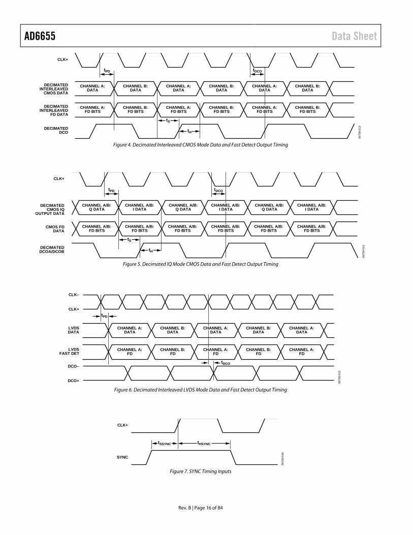
Figure 4. Decimated Interleaved CMOS Mode Data and Fast Detect Output Timing
tPD tDCO
tH
tS
CLK+
DECIMATEDCMOS IQ
OUTPUT DATA
CHANNEL A/B:I DATA
CHANNEL A/B:Q DATA
CHANNEL A/B:Q DATA
CHANNEL A/B:I DATA
CHANNEL A/B:Q DATA
CHANNEL A/B:FD BITS
CHANNEL A/B:FD BITS
CHANNEL A/B:FD BITS
CHANNEL A/B:FD BITS
CHANNEL A/B:FD BITS
CMOS FDDATA
DECIMATEDDCOA/DCOB
CHANNEL A/B:I DATA
CHANNEL A/B:FD BITS
0670
9-01
4
Figure 5. Decimated IQ Mode CMOS Data and Fast Detect Output Timing
tPD
tDCO
CLK–
CLK+
LVDSDATA
CHANNEL A:DATA
CHANNEL B:DATA
CHANNEL A:DATA
LVDSFAST DET
DCO–
DCO+
CHANNEL B:DATA
CHANNEL A:FD
CHANNEL B:FD
CHANNEL A:FD
CHANNEL B:FD
CHANNEL A:DATA
CHANNEL A:FD
0670
9-01
5
Figure 6. Decimated Interleaved LVDS Mode Data and Fast Detect Output Timing
tSSYNC tHSYNC
SYNC
CLK+
0670
9-01
6
Figure 7. SYNC Timing Inputs

Data Sheet AD6655
Rev. B | Page 17 of 84
tCSSCLK
tSSCLKSDFS tSSCLKSDFS
CLK+
CLK–
SMI SCLK
SMI SDFS
SMI SDO DATA DATA
0670
9-01
7
Figure 8. Signal Monitor SPORT Output Timing

AD6655 Data Sheet
Rev. B | Page 18 of 84
ABSOLUTE MAXIMUM RATINGS Table 10. Parameter Rating ELECTRICAL
AVDD, DVDD to AGND −0.3 V to +2.0 V DRVDD to DRGND −0.3 V to +3.9 V AGND to DRGND −0.3 V to +0.3 V VIN+A/VIN+B, VIN-A/VIN−B to AGND −0.3 V to AVDD + 0.2 V CLK+, CLK− to AGND −0.3 V to +3.9 V SYNC to AGND −0.3 V to +3.9 V VREF to AGND −0.3 V to AVDD + 0.2 V SENSE to AGND −0.3 V to AVDD + 0.2 V CML to AGND −0.3 V to AVDD + 0.2 V RBIAS to AGND −0.3 V to AVDD + 0.2 V CSB to AGND −0.3 V to +3.9 V SCLK/DFS to DRGND −0.3 V to +3.9 V SDIO/DCS to DRGND −0.3 V to DRVDD + 0.3 V SMI SDO/OEB to DRGND −0.3 V to DRVDD + 0.3 V SMI SCLK/PDWN to DRGND −0.3 V to DRVDD + 0.3 V SMI SDFS to DRGND −0.3 V to DRVDD + 0.3 V D0A/D0B through D13A/D13B
to DRGND −0.3 V to DRVDD + 0.3 V
FD0A/FD0B through FD3A/FD3B to DRGND
−0.3 V to DRVDD + 0.3 V
DCOA/DCOB to DRGND −0.3 V to DRVDD + 0.3 V ENVIRONMENTAL
Operating Temperature Range (Ambient)
−40°C to +85°C
Maximum Junction Temperature Under Bias
150°C
Storage Temperature Range (Ambient)
−65°C to +125°C
Stresses above those listed under Absolute Maximum Ratings may cause permanent damage to the device. This is a stress rating only; functional operation of the device at these or any other conditions above those indicated in the operational section of this specification is not implied. Exposure to absolute maximum rating conditions for extended periods may affect device reliability.
THERMAL CHARACTERISTICS The exposed paddle must be soldered to the ground plane for the LFCSP package. Soldering the exposed paddle to the customer board increases the reliability of the solder joints, maximizing the thermal capability of the package.
Table 11. Thermal Resistance
Package Type
Airflow Velocity (m/s) θJA
1, 2 θJC1, 3 θJB
1, 4 Unit 64-Lead LFCSP
9 mm × 9 mm (CP-64-6)
0 18.8 0.6 6.0 °C/W 1.0 16.5 °C/W 2.0 15.8 °C/W
1 Per JEDEC 51-7, plus JEDEC 25-5 2S2P test board. 2 Per JEDEC JESD51-2 (still air) or JEDEC JESD51-6 (moving air). 3 Per MIL-Std 883, Method 1012.1. 4 Per JEDEC JESD51-8 (still air).
Typical θJA is specified for a 4-layer PCB with solid ground plane. As shown, airflow increases heat dissipation, which reduces θJA. In addition, metal in direct contact with the package leads from metal traces, through holes, ground, and power planes, reduces the θJA.
ESD CAUTION

Data Sheet AD6655
Rev. B | Page 19 of 84
PIN CONFIGURATIONS AND FUNCTION DESCRIPTIONS
17 18 19 20 21 22 23 24 25 26 27 28 29 30 31 32
D5A
D6A
D7A
DR
GN
DD
RVD
DD
8AD
9AD
VDD
D10
AD
11A
D12
AD
13A
(MSB
)FD
0AFD
1AFD
2AFD
3A
64 63 62 61 60 59 58 57 56 55 54 53 52 51 50 49
DR
GN
DD
5BD
4BD
3BD
2BD
1BD
0B (L
SB)
DVD
DFD
3BFD
2BFD
1BFD
0BSY
NC
CSB
CLK
–C
LK+
123456789
10111213141516
DRVDDD6BD7BD8BD9B
D10BD11BD12B
D13B (MSB)DCOBDCOA
D0A (LSB)D1AD2AD3AD4A
SCLK/DFSSDIO/DCSAVDDAVDDVIN+BVIN–BRBIASCMLSENSEVREFVIN–AVIN+AAVDDSMI SDFSSMI SCLK/PDWNSMI SDO/OEB
48474645444342414039383736353433
PIN 1INDICATOR
AD6655PARALLEL CMOS
TOP VIEW(Not to Scale)
EXPOSED PADDLE, PIN 0(BOTTOM OF PACKAGE)
0670
9-00
2
NOTES1. THE EXPOSED THERMAL PAD ON THE BOTTOM OF THE PACKAGE PROVIDES THE
ANALOG GROUND FOR THE PART. THIS EXPOSED PAD MUST BE CONNECTED TO GROUND FOR PROPER OPERATION.
Figure 9. LFCSP Parallel CMOS Pin Configuration (Top View)
Table 12. Pin Function Descriptions (Parallel CMOS Mode) Pin No. Mnemonic Type Description ADC Power Supplies 20, 64 DRGND Ground Digital Output Ground. 1, 21 DRVDD Supply Digital Output Driver Supply (1.8 V to 3.3 V). 24, 57 DVDD Supply Digital Power Supply (1.8 V Nominal). 36, 45, 46 AVDD Supply Analog Power Supply (1.8 V Nominal). 0 AGND,
Exposed Pad Ground Analog Ground. The exposed thermal pad on the bottom of the package provides the
analog ground for the part. This pad must be connected to ground for proper operation. ADC Analog 37 VIN+A Input Differential Analog Input Pin (+) for Channel A. 38 VIN−A Input Differential Analog Input Pin (−) for Channel A. 44 VIN+B Input Differential Analog Input Pin (+) for Channel B. 43 VIN−B Input Differential Analog Input Pin (−) for Channel B. 39 VREF Input/Output Voltage Reference Input/Output. 40 SENSE Input Voltage Reference Mode Select. (See Table 15 for details.) 42 RBIAS Input/Output External Reference Bias Resistor. 41 CML Output Common-Mode Level Bias Output for Analog Inputs. 49 CLK+ Input ADC Clock Input—True. 50 CLK− Input ADC Clock Input—Complement. ADC Fast Detect Outputs 29 FD0A Output Channel A Fast Detect Indicator. (See Table 21 for details.) 30 FD1A Output Channel A Fast Detect Indicator. (See Table 21 for details.) 31 FD2A Output Channel A Fast Detect Indicator. (See Table 21 for details.) 32 FD3A Output Channel A Fast Detect Indicator. (See Table 21 for details.) 53 FD0B Output Channel B Fast Detect Indicator. (See Table 21 for details.) 54 FD1B Output Channel B Fast Detect Indicator. (See Table 21 for details.) 55 FD2B Output Channel B Fast Detect Indicator. (See Table 21 for details.) 56 FD3B Output Channel B Fast Detect Indicator. (See Table 21 for details.)

AD6655 Data Sheet
Rev. B | Page 20 of 84
Pin No. Mnemonic Type Description Digital Input 52 SYNC Input Digital Synchronization Pin. Slave mode only. Digital Outputs 12 D0A (LSB) Output Channel A CMOS Output Data. 13 D1A Output Channel A CMOS Output Data. 14 D2A Output Channel A CMOS Output Data. 15 D3A Output Channel A CMOS Output Data. 16 D4A Output Channel A CMOS Output Data. 17 D5A Output Channel A CMOS Output Data. 18 D6A Output Channel A CMOS Output Data. 19 D7A Output Channel A CMOS Output Data. 22 D8A Output Channel A CMOS Output Data. 23 D9A Output Channel A CMOS Output Data. 25 D10A Output Channel A CMOS Output Data. 26 D11A Output Channel A CMOS Output Data. 27 D12A Output Channel A CMOS Output Data. 28 D13A (MSB) Output Channel A CMOS Output Data. 58 D0B (LSB) Output Channel B CMOS Output Data. 59 D1B Output Channel B CMOS Output Data. 60 D2B Output Channel B CMOS Output Data. 61 D3B Output Channel B CMOS Output Data. 62 D4B Output Channel B CMOS Output Data. 63 D5B Output Channel B CMOS Output Data. 2 D6B Output Channel B CMOS Output Data. 3 D7B Output Channel B CMOS Output Data. 4 D8B Output Channel B CMOS Output Data. 5 D9B Output Channel B CMOS Output Data. 6 D10B Output Channel B CMOS Output Data. 7 D11B Output Channel B CMOS Output Data. 8 D12B Output Channel B CMOS Output Data. 9 D13B (MSB) Output Channel B CMOS Output Data. 11 DCOA Output Channel A Data Clock Output. 10 DCOB Output Channel B Data Clock Output. SPI Control 48 SCLK/DFS Input SPI Serial Clock/Data Format Select Pin in External Pin Mode.
47 SDIO/DCS Input/Output SPI Serial Data I/O/Duty Cycle Stabilizer Pin in External Pin Mode. 51 CSB Input SPI Chip Select. Active low. Signal Monitor Port 33 SMI SDO/OEB Input/Output Signal Monitor Serial Data Output/Output Enable Input (Active Low) in External Pin Mode. 35 SMI SDFS Output Signal Monitor Serial Data Frame Sync. 34 SMI SCLK/PDWN Input/Output Signal Monitor Serial Clock Output/Power-Down Input (Active High) in External Pin Mode.

Data Sheet AD6655
Rev. B | Page 21 of 84
PIN 1INDICATOR
17 18 19 20 21 22 23 24 25 26 27 28 29 30 31 32
D7+ D8–
D8+
DR
GN
DD
RVD
DD
9–D
9+D
VDD
D10
–D
10+
D11
–D
11+
D12
–D
12+
D13
– (M
SB)
D13
+ (M
SB)
64 63 62 61 60 59 58 57 56 55 54 53 52 51 50 49
DR
GN
DD
0+ (L
SB)
D0–
(LSB
)FD
3+FD
3–FD
2+FD
2–D
VDD
FD1+
FD1–
FD0+
FD0–
SYN
CC
SBC
LK–
CLK
+
123456789
10111213141516
DRVDDD1–D1+D2–D2+D3–D3+D4–D4+
DCO–DCO+
D5–D5+D6–D6+D7–
SCLK/DFSSDIO/DCSAVDDAVDDVIN+BVIN–BRBIASCMLSENSEVREFVIN–AVIN+AAVDDSMI SDFSSMI SCLK/PDWNSMI SDO/OEB
48474645444342414039383736353433
AD6655PARALLEL LVDS
TOP VIEW(Not to Scale)
EXPOSED PADDLE, PIN 0(BOTTOM OF PACKAGE)
0670
9-00
3
NOTES1. THE EXPOSED THERMAL PAD ON THE BOTTOM OF THE PACKAGE PROVIDES THE
ANALOG GROUND FOR THE PART. THIS EXPOSED PAD MUST BE CONNECTED TO GROUND FOR PROPER OPERATION.
Figure 10. LFCSP Interleaved Parallel LVDS Pin Configuration (Top View)
Table 13. Pin Function Descriptions (Interleaved Parallel LVDS Mode) Pin No. Mnemonic Type Description ADC Power Supplies 20, 64 DRGND Ground Digital Output Ground. 1, 21 DRVDD Supply Digital Output Driver Supply (1.8 V to 3.3 V). 24, 57 DVDD Supply Digital Power Supply (1.8 V Nominal.) 36, 45, 46 AVDD Supply Analog Power Supply (1.8 V Nominal.) 0 AGND,
Exposed Pad Ground Analog Ground. The exposed thermal pad on the bottom of the package provides the analog
ground for the part. This exposed pad must be connected to ground for proper operation. ADC Analog 37 VIN+A Input Differential Analog Input Pin (+) for Channel A. 38 VIN−A Input Differential Analog Input Pin (−) for Channel A. 44 VIN+B Input Differential Analog Input Pin (+) for Channel B. 43 VIN−B Input Differential Analog Input Pin (−) for Channel B. 39 VREF Input/Output Voltage Reference Input/Output. 40 SENSE Input Voltage Reference Mode Select. See Table 15 for details. 42 RBIAS Input/Output External Reference Bias Resistor. 41 CML Output Common-Mode Level Bias Output for Analog Inputs. 49 CLK+ Input ADC Clock Input—True. 50 CLK− Input ADC Clock Input—Complement. ADC Fast Detect Outputs 54 FD0+ Output Channel A/Channel B LVDS Fast Detect Indicator 0—True. See Table 21 for details. 53 FD0- Output Channel A/Channel B LVDS Fast Detect Indicator 0—Complement. See Table 21 for details. 56 FD1+ Output Channel A/Channel B LVDS Fast Detect Indicator 1—True. See Table 21 for details. 55 FD1− Output Channel A/Channel B LVDS Fast Detect Indicator 1—Complement. See Table 21 for details. 59 FD2+ Output Channel A/Channel B LVDS Fast Detect Indicator 2—True See Table 21 for details. 58 FD2− Output Channel A/Channel B LVDS Fast Detect Indicator 2—Complement. See Table 21 for details. 61 FD3+ Output Channel A/Channel B LVDS Fast Detect Indicator 3—True. See Table 21 for details. 60 FD3− Output Channel A/Channel B LVDS Fast Detect Indicator 3—Complement. See Table 21 for details.
AD6655 Data Sheet
Rev. B | Page 22 of 84
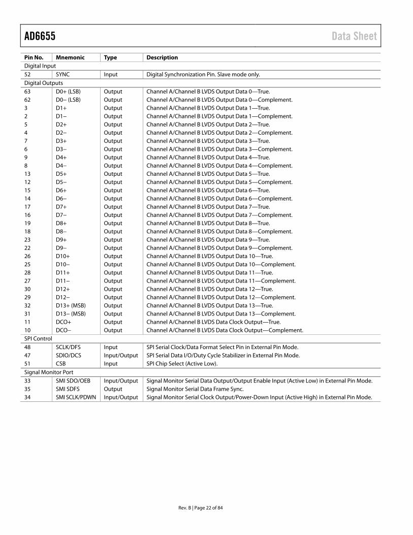
Pin No. Mnemonic Type Description Digital Input 52 SYNC Input Digital Synchronization Pin. Slave mode only. Digital Outputs 63 D0+ (LSB) Output Channel A/Channel B LVDS Output Data 0—True. 62 D0− (LSB) Output Channel A/Channel B LVDS Output Data 0—Complement. 3 D1+ Output Channel A/Channel B LVDS Output Data 1—True. 2 D1− Output Channel A/Channel B LVDS Output Data 1—Complement. 5 D2+ Output Channel A/Channel B LVDS Output Data 2—True. 4 D2− Output Channel A/Channel B LVDS Output Data 2—Complement. 7 D3+ Output Channel A/Channel B LVDS Output Data 3—True. 6 D3− Output Channel A/Channel B LVDS Output Data 3—Complement. 9 D4+ Output Channel A/Channel B LVDS Output Data 4—True. 8 D4− Output Channel A/Channel B LVDS Output Data 4—Complement. 13 D5+ Output Channel A/Channel B LVDS Output Data 5—True. 12 D5− Output Channel A/Channel B LVDS Output Data 5—Complement. 15 D6+ Output Channel A/Channel B LVDS Output Data 6—True. 14 D6− Output Channel A/Channel B LVDS Output Data 6—Complement. 17 D7+ Output Channel A/Channel B LVDS Output Data 7—True. 16 D7− Output Channel A/Channel B LVDS Output Data 7—Complement. 19 D8+ Output Channel A/Channel B LVDS Output Data 8—True. 18 D8− Output Channel A/Channel B LVDS Output Data 8—Complement. 23 D9+ Output Channel A/Channel B LVDS Output Data 9—True. 22 D9− Output Channel A/Channel B LVDS Output Data 9—Complement. 26 D10+ Output Channel A/Channel B LVDS Output Data 10—True. 25 D10− Output Channel A/Channel B LVDS Output Data 10—Complement. 28 D11+ Output Channel A/Channel B LVDS Output Data 11—True. 27 D11− Output Channel A/Channel B LVDS Output Data 11—Complement. 30 D12+ Output Channel A/Channel B LVDS Output Data 12—True. 29 D12− Output Channel A/Channel B LVDS Output Data 12—Complement. 32 D13+ (MSB) Output Channel A/Channel B LVDS Output Data 13—True. 31 D13− (MSB) Output Channel A/Channel B LVDS Output Data 13—Complement. 11 DCO+ Output Channel A/Channel B LVDS Data Clock Output—True. 10 DCO− Output Channel A/Channel B LVDS Data Clock Output—Complement. SPI Control 48 SCLK/DFS Input SPI Serial Clock/Data Format Select Pin in External Pin Mode. 47 SDIO/DCS Input/Output SPI Serial Data I/O/Duty Cycle Stabilizer in External Pin Mode. 51 CSB Input SPI Chip Select (Active Low). Signal Monitor Port 33 SMI SDO/OEB Input/Output Signal Monitor Serial Data Output/Output Enable Input (Active Low) in External Pin Mode. 35 SMI SDFS Output Signal Monitor Serial Data Frame Sync. 34 SMI SCLK/PDWN Input/Output Signal Monitor Serial Clock Output/Power-Down Input (Active High) in External Pin Mode.
Data Sheet AD6655
Rev. B | Page 23 of 84
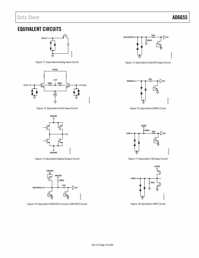
EQUIVALENT CIRCUITS VIN
0670
9-00
4
Figure 11. Equivalent Analog Input Circuit
1.2V10kΩ 10kΩ
CLK+ CLK–
AVDD
0670
9-00
5
Figure 12. Equivalent Clock lnput Circuit
DRVDD
DRGND 0670
9-00
6
Figure 13. Equivalent Digital Output Circuit
SDIO/DCS1kΩ
26kΩ
DRVDD
DRVDD
0670
9-00
7
Figure 14. Equivalent SDIO/DCS Circuit or SMI SDFS Circuit
SCLK/DFS1kΩ
26kΩ
0670
9-00
8
Figure 15. Equivalent SCLK/DFS Input Circuit
SENSE1kΩ
0670
9-00
9
Figure 16. Equivalent SENSE Circuit
CSB1kΩ26kΩ
AVDD
0670
9-01
0
Figure 17. Equivalent CSB Input Circuit
VREF
AVDD
6kΩ
0670
9-01
1
Figure 18. Equivalent VREF Circuit
.
AD6655 Data Sheet
Rev. B | Page 24 of 84
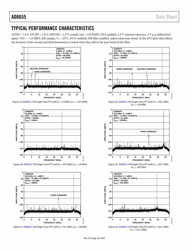
TYPICAL PERFORMANCE CHARACTERISTICSAVDD = 1.8 V, DVDD = 1.8 V, DRVDD = 1.8 V, sample rate = 150 MSPS, DCS enabled, 1.0 V internal reference, 2 V p-p differential input, VIN = −1.0 dBFS, 64k sample, TA = 25°C, NCO enabled, FIR filter enabled, unless otherwise noted. In the FFT plots that follow, the location of the second and third harmonics is noted when they fall in the pass band of the filter.
0
–20
–40
–60
–80
–100
–120
–1400 3530252015105
AM
PLIT
UD
E (d
BFS
)
FREQUENCY (MHz)
150MSPS2.4MHz @ –1dBFSSNR = 74.7dBc (75.7dBFS)SFDR = 86.5dBcfNCO = 18.75MHz
SECOND HARMONICTHIRD HARMONIC
0670
9-01
8
Figure 19. AD6655-150 Single-Tone FFT with fIN = 2.4 MHz, fNCO = 18.75 MHz
0
–20
–40
–60
–80
–100
–120
–1400 3530252015105
AM
PLIT
UD
E (d
BFS
)
FREQUENCY (MHz)
150MSPS30.3MHz @ –1dBFSSNR = 74.8dBc (75.8dBFS)SFDR = 100dBcfNCO = 24MHz
0670
9-01
9
Figure 20. AD6655-150 Single-Tone FFT with fIN = 30.3 MHz, fNCO = 24 MHz
0
–20
–40
–60
–80
–100
–120
–1400 3530252015105
AM
PLIT
UD
E (d
BFS
)
FREQUENCY (MHz)
150MSPS140.1MHz @ –1dBFSSNR = 74.3dBc (75.3dBFS)SFDR = 83.3dBcfNCO = 56MHz
THIRD HARMONIC
0670
9-02
0
Figure 21. AD6655-150 Single-Tone FFT with fIN = 70.1 MHz, fNCO = 56 MHz
0
–20
–40
–60
–80
–100
–120
–1400 3530252015105
AM
PLIT
UD
E (d
BFS
)
FREQUENCY (MHz)
150MSPS140.1MHz @ –1dBFSSNR = 73.7dBc (74.7dBFS)SFDR = 82.8dBcfNCO = 126MHz
SECOND HARMONICTHIRD HARMONIC
0670
9-02
1
Figure 22. AD6655-150 Single-Tone FFT with fIN = 140.1 MHz,
fNCO = 126 MHz
0
–20
–40
–60
–80
–100
–120
–1400 3530252015105
AM
PLIT
UD
E (d
BFS
)
FREQUENCY (MHz)
150MSPS220.1MHz @ –1dBFSSNR = 71.8dBc (72.8dBFS)SFDR = 81.4dBcfNCO = 205MHz
THIRD HARMONIC
0670
9-02
2
Figure 23. AD6655-150 Single-Tone FFT with fIN = 220.1 MHz,
fNCO = 205 MHz
0
–20
–40
–60
–80
–100
–120
–1400 3530252015105
AM
PLIT
UD
E (d
BFS
)
FREQUENCY (MHz)
150MSPS332.1MHz @ –1dBFSSNR = 71.7dBc (72.7dBFS)SFDR = 95.0dBcfNCO = 321.5MHz
0670
9-02
3
Figure 24. AD6655-150 Single-Tone FFT with fIN = 332.1 MHz,
fNCO = 321.5 MHz

Data Sheet AD6655
Rev. B | Page 25 of 84
0
–20
–40
–60
–80
–100
–120
–1400 3530252015105
AM
PLIT
UD
E (d
BFS
)
FREQUENCY (MHz)
150MSPS445.1MHz @ –1dBFSSNR = 67.4dBc (65.4dBFS)SFDR = 74.1dBcfNCO = 429MHz
SECOND HARMONIC
THIRD HARMONIC
0670
9-02
4
Figure 25. AD6655-150 Single-Tone FFT with fIN = 445.1 MHz, fNCO = 429 MHz
0
–20
–40
–60
–80
–100
–120
–1400 30252015105
AM
PLIT
UD
E (d
BFS
)
FREQUENCY (MHz)
125MSPS2.4MHz @ –1dBFSSNR = 74.5dBc (75.5dBFS)SFDR = 87.8dBcfNCO = 15.75MHz
SECOND HARMONICTHIRD HARMONIC
0670
9-02
5
Figure 26. AD6655-125 Single-Tone FFT with fIN =2.4 MHz, fNCO = 15.75 MHz
0
–20
–40
–60
–80
–100
–120
–1400 30252015105
AM
PLIT
UD
E (d
BFS
)
FREQUENCY (MHz)
125MSPS30.3MHz @ –1dBFSSNR = 74.7dBc (75.7dBFS)SFDR = 89.6dBcfNCO = 21MHz
THIRDHARMONIC
0670
9-02
6
Figure 27. AD6655-125 Single-Tone FFT with fIN = 30.3 MHz, fNCO = 21 MHz
0
–20
–40
–60
–80
–100
–120
–1400 30252015105
AM
PLIT
UD
E (d
BFS
)
FREQUENCY (MHz)
125MSPS70.3MHz @ –1dBFSSNR = 74.6dBc (75.6dBFS)SFDR = 86.1dBcfNCO = 78MHz
THIRD HARMONIC
0670
9-02
7
Figure 28. AD6655-125 Single-Tone FFT with fIN = 70.3 MHz, fNCO = 78 MHz
0
–20
–40
–60
–80
–100
–120
–1400 30252015105
AM
PLIT
UD
E (d
BFS
)
FREQUENCY (MHz)
125MSPS140.1MHz @ –1dBFSSNR = 74.1dBc (75.1dBFS)SFDR = 90.3dBcfNCO = 142MHz
THIRD HARMONIC
0670
9-02
8
Figure 29. AD6655-125 Single-Tone FFT with fIN = 140.1 MHz, fNCO = 142 MHz
0
–20
–40
–60
–80
–100
–120
–1400 30252015105
AM
PLIT
UD
E (d
BFS
)
FREQUENCY (MHz)
125MSPS220.1MHz @ –1dBFSSNR = 73.4dBc (74.4dBFS)SFDR = 90.2dBcfNCO = 231MHz
0670
9-02
9
Figure 30. AD6655-125 Single-Tone FFT with fIN = 220.1 MHz, fNCO = 231 MHz

AD6655 Data Sheet
Rev. B | Page 26 of 84
120
0
20
40
60
80
100
–90 0–10–20–30–40–50–60–70–80
SNR
/SFD
R (d
Bc
AN
D d
BFS
)
INPUT AMPLITUDE (dBFS)
SFDR (dBc)
SFDR (dBFS)
SNR (dBFS)
SNR (dBc)
85dBREFERENCE LINE
0670
9-03
0
Figure 31. AD6655-150 Single-Tone SNR/SFDR vs. Input Amplitude (AIN) with
fIN = 2.4 MHz, fNCO = 18.75 MHz
120
0
20
40
60
80
100
–90 0–10–20–30–40–50–60–70–80
SNR
/SFD
R (d
Bc
AN
D d
BFS
)
INPUT AMPLITUDE (dBFS)
SFDR (dBc)
SFDR (dBFS)
SNR (dBFS)
SNR (dBc)
85dBREFERENCE LINE
0670
9-03
1
Figure 32. AD6655-150 Single-Tone SNR/SFDR vs. Input Amplitude (AIN) with
fIN = 98.12 MHz, fNCO = 100.49 MHz
95
90
85
80
75
70
65
600 45040035030025020015010050
SNR
/SFD
R (d
Bc)
INPUT FREQUENCY (MHz)
SFDR = +25°C
SFDR = +85°C
SFDR = –40°C
SNR = +25°CSNR = +85°CSNR = –40°C
0670
9-03
2
Figure 33. AD6655-125 Single-Tone SNR/SFDR vs. Input Frequency (fIN) and
Temperature with DRVDD = 1.8 V
95
90
85
80
75
70
65
600 45040035030025020015010050
SNR
/SFD
R (d
Bc)
INPUT FREQUENCY (MHz)
SFDR = +25°C
SFDR = +85°C
SFDR = –40°C
SNR = +25°CSNR = +85°CSNR = –40°C
0670
9-03
3
Figure 34. AD6655-125 Single-Tone SNR/SFDR vs. Input Frequency (fIN) and
Temperature with DRVDD = 3.3 V
–1.5
–4.0
–3.5
–3.0
–2.5
–2.0
0.5
0
0.1
0.2
0.3
0.4
–40 806040200–20
GA
IN E
RR
OR
(%FS
R)
OFF
SET
ERR
OR
(%FS
R)
TEMPERATURE (°C) 0670
9-03
4
OFFSET
GAIN
Figure 35. AD6655-150 Gain and Offset vs. Temperature
0
–120
–100
–80
–60
–40
–20
–90 –78 –66 –54 –42 –30 –18 –6
SFD
R/IM
D3
(dB
c A
ND
dB
FS)
INPUT AMPLITUDE (dBFS)
SFDR (dBc)
SFDR (dBFS) IMD3 (dBFS)
IMD3 (dBc)06
709-
035
Figure 36. AD6655-150 Two-Tone SFDR/IMD3 vs. Input Amplitude (AIN) with
fIN1 = 29.12 MHz, fIN2 = 32.12 MHz, fS = 150 MSPS, fNCO = 22 MHz

Data Sheet AD6655
Rev. B | Page 27 of 84
0
–120
–100
–80
–60
–40
–20
–90 –78 –66 –54 –42 –30 –18 –6
SFD
R/IM
D3
(dB
c A
ND
dB
FS)
INPUT AMPLITUDE (dBFS)
SFDR (dBc)
SFDR (dBFS) IMD3 (dBFS)
IMD3 (dBc)
0670
9-03
6
Figure 37. AD6655-150 Two-Tone SFDR/IMD3 vs. Input Amplitude (AIN) with
fIN1 = 169.12 MHz, fIN2 = 172.12 MHz, fS = 150 MSPS, fNCO = 177 MHz
0
–20
–40
–60
–80
–100
–120
–1400 5 10 15 20 25 30
0670
9-03
7
AM
PLIT
UD
E (d
BFS
)
FREQUENCY (MHz)
Figure 38. AD6655-125, Two 64k WCDMA Carriers with fIN = 170 MHz, fS = 122.88 MHz, fNCO = 168.96 MHz
0
–20
–40
–60
–80
–100
–120
–1400 3530252015105
AM
PLIT
UD
E (d
BFS
)
FREQUENCY (MHz)
150MSPS29.12MHz @ –7dBFS32.12MHz @ –7dBFSSFDR = 89.1dBc (96.1dBFS)fNCO = 22MHz
0670
9-03
8
Figure 39. AD6655-150 Two-Tone FFT with fIN1 = 29.12 MHz, fIN2 = 32.12 MHz,
fS = 150 MSPS, fNCO = 22 MHz
0
–20
–40
–60
–80
–100
–120
–1400 3530252015105
AM
PLIT
UD
E (d
BFS
)
FREQUENCY (MHz)
150MSPS169.12MHz @ –7dBFS172.12MHz @ –7dBFSSFDR = 85.5dBc (92.5dBFS)fNCO = 177MHz
0670
9-03
9
Figure 40. AD6655-150 Two Tone FFT with fIN1 = 169.12 MHz,
fIN2 = 172.12 MHz, fS = 150 MSPS, fNCO = 177 MHz
0
–20
–40
–60
–80
–100
–120
–1400 37.530.022.515.07.5
AM
PLIT
UD
E (d
BFS
)
FREQUENCY (MHz)
NPR = 64.5dBcNOTCH @ 18.5MHzNOTCH WIDTH = 3MHz
0670
9-04
0
Figure 41. AD6655-150 Noise Power Ratio (NPR)
95
85
75
650 25 50 75 100 125 150
0670
9-04
1
SNR
/SFD
R (d
Bc)
SAMPLE RATE (MSPS)
SFDR (dBc)
SNR (dBc)
Figure 42. AD6655-150 Single-Tone SNR/SFDR vs. Sample Rate (fs) with fIN = 2.3 MHz

AD6655 Data Sheet
Rev. B | Page 28 of 84
12
0
2
4
6
8
10
NU
MB
ER O
F H
ITS
(1M
)
OUTPUT CODEN – 3 N – 2 N – 1 N N + 1 N + 2 N + 3
0.85 LSB rms
0670
9-04
2
Figure 43. AD6655 Grounded Input Histogram
90
85
80
75
70
SNR
/SFD
R (d
Bc)
DUTY CYCLE (%)
SFDR DCS ON
SNR DCS ON
SFDR DCS OFF
SNR DCS OFF
20 30 40 50 60 70 80
0670
9-04
3
Figure 44. AD6655-150 SNR/SFDR vs. Duty Cycle with fIN = 30.3 MHz,
fNCO = 45 MHz
90
85
80
75
65
70
SNR
/SFD
R (d
Bc)
INPUT COMMON-MODE VOLTAGE (V)
SNR
SFDR
0.2 0.4 0.6 0.8 1.0 1.2 1.4
0670
9-04
4
Figure 45. AD6655-150 SNR/SFDR vs. Input Common Mode (VCM) with
fIN = 30.3 MHz, fNCO = 45 MHz

Data Sheet AD6655
Rev. B | Page 29 of 84
THEORY OF OPERATION The AD6655 has two analog input channels, two decimating channels, and two digital output channels. The intermediate frequency (IF) input signal passes through several stages before appearing at the output port(s) as a filtered, decimated digital signal.
The dual ADC design can be used for diversity reception of signals, where the ADCs operate identically on the same carrier but from two separate antennae. The ADCs can also be operated with independent analog inputs. The user can sample any fS/2 frequency segment from dc to 150 MHz using appropriate low-pass or band-pass filtering at the ADC inputs with little loss in ADC performance. Operation to 450 MHz analog input is permitted but occurs at the expense of increased ADC noise and distortion.
In nondiversity applications, the AD6655 can be used as a base-band receiver, where one ADC is used for I input data, and the other is used for Q input data.
Synchronization capability is provided to allow synchronized timing between multiple channels or multiple devices. The NCO phase can be set to produce a known offset relative to another channel or device.
Programming and control of the AD6655 are accomplished using a 3-bit SPI-compatible serial interface.
ADC ARCHITECTURE AD6655 architecture consists of a front-end sample-and-hold amplifier (SHA) followed by a pipelined, switched-capacitor ADC. The quantized outputs from each stage are combined into a final 14-bit result in the digital correction logic. The pipelined archi-tecture permits the first stage to operate on a new input sample and the remaining stages to operate on the preceding samples. Sampling occurs on the rising edge of the clock.
Each stage of the pipeline, excluding the last, consists of a low resolution flash ADC connected to a switched-capacitor digital-to-analog converter (DAC) and an interstage residue amplifier (MDAC). The residue amplifier magnifies the difference between the reconstructed DAC output and the flash input for the next stage in the pipeline. One bit of redundancy is used in each stage to facilitate digital correction of flash errors. The last stage simply consists of a flash ADC.
The input stage of each channel contains a differential SHA that can be ac- or dc-coupled in differential or single-ended modes. The output staging block aligns the data, corrects errors, and passes the data to the output buffers. The output buffers are powered from a separate supply, allowing adjustment of the output voltage swing. During power-down, the output buffers go into a high impedance state.
ANALOG INPUT CONSIDERATIONS The analog input to the AD6655 is a differential switched-capacitor SHA that has been designed for optimum performance while processing a differential input signal.
The clock signal alternatively switches the SHA between sample mode and hold mode (see Figure 46). When the SHA is switched into sample mode, the signal source must be capable of charging the sample capacitors and settling within 1/2 of a clock cycle.
A small resistor in series with each input can help reduce the peak transient current required from the output stage of the driving source. A shunt capacitor can be placed across the inputs to provide dynamic charging currents. This passive network creates a low-pass filter at the ADC input; therefore, the precise values are dependent on the application.
In IF undersampling applications, any shunt capacitors should be reduced. In combination with the driving source impedance, the shunt capacitors limit the input bandwidth. Refer to Appli-cation Note AN-742, Frequency Domain Response of Switched-Capacitor ADCs; Application Note AN-827, A Resonant Approach to Interfacing Amplifiers to Switched-Capacitor ADCs; and the Analog Dialogue article, “Transformer-Coupled Front-End for Wideband A/D Converters,” for more information on this subject (see www.analog.com). In general, the precise values are dependent on the application.
VIN+
VIN–
CPIN, PAR
CPIN, PAR
CS
CS
CH
CH
H
S
S
S
S 0670
9-04
8
Figure 46. Switched-Capacitor SHA Input
For best dynamic performance, the source impedances driving VIN+ and VIN− should be matched such that common-mode settling errors are symmetrical. These errors are reduced by the common-mode rejection of the ADC.
An internal differential reference buffer creates positive and negative reference voltages that define the input span of the ADC core. The output common mode of the reference buffer is set to VCMREF (approximately 1.6 V).
Input Common Mode
The analog inputs of the AD6655 are not internally dc biased. In ac-coupled applications, the user must provide this bias externally. Setting the device so that VCM = 0.55 × AVDD is recommended for optimum performance, but the device functions over a wider range with reasonable performance (see Figure 45).

AD6655 Data Sheet
Rev. B | Page 30 of 84
An on-board common-mode voltage reference is included in the design and is available from the CML pin. Optimum perform-ance is achieved when the common-mode voltage of the analog input is set by the CML pin voltage (typically 0.55 × AVDD).
Differential Input Configurations
Optimum performance is achieved while driving the AD6655 in a differential input configuration. For baseband applications, the AD8138, ADA4937-2, and ADA4938-2 differential drivers provide excellent performance and a flexible interface to the ADC. The output common-mode voltage of the AD8138 is easily set with the CML pin of the AD6655 (see Figure 47), and the driver can be configured in a Sallen-Key filter topology to provide band limiting of the input signal.
AVDD1V p-p 49.9Ω
523Ω0.1µF
R
R
C
499Ω
499Ω
499Ω
AD8138 AD6655
VIN+
VIN– CML
0670
9-04
9
Figure 47. Differential Input Configuration Using the AD8138
For baseband applications where SNR is a key parameter, differential transformer coupling is the recommended input configuration. An example is shown in Figure 48. To bias the analog input, the CML voltage can be connected to the center tap of the secondary winding of the transformer.
2V p-p 49.9Ω
0.1µF
R
RC AD6655
VIN+
VIN– CML
0670
9-05
0
Figure 48. Differential Transformer-Coupled Configuration
The signal characteristics must be considered when selecting a transformer. Most RF transformers saturate at frequencies below a few megahertz (MHz). Excessive signal power can also cause core saturation, which leads to distortion.
At input frequencies in the second Nyquist zone and above, the noise performance of most amplifiers is not adequate to achieve the true SNR performance of the AD6655. For applications where SNR is a key parameter, differential double balun coupling is the recommended input configuration (see Figure 49).
An alternative to using a transformer-coupled input at frequencies in the second Nyquist zone is to use the AD8352 differential driver is shown in Figure 50. See the AD8352 data sheet for more information. In addition, if the application requires an amplifier with variable gain, the AD8375 or AD8376 digital variable gain amplifiers (DVGAs) provide good performance driving the AD6655.
In any configuration, the value of the shunt capacitor, C, is dependent on the input frequency and source impedance and may need to be reduced or removed. Table 14 displays recom-mended values to set the RC network. However, these values are dependent on the input signal and should be used only as a starting guide.
Table 14. Example RC Network Frequency Range (MHz)
R Series (Ω, Each)
C Differential (pF)
0 to 70 33 15 70 to 200 33 5 200 to 300 15 5 >300 15 Open
AD6655
R0.1µF0.1µF2V p-p VIN+
VIN– CML
C
R0.1µF
S0.1µF25Ω
25Ω
SPA P
0670
9-05
1
Figure 49. Differential Double Balun Input Configuration
AD6655AD8352
0ΩR
0Ω
CD RD RG
0.1µF
0.1µF
0.1µF
VIN+
VIN– CML
C
0.1µF
1612
345
11
R0.1µF
0.1µF
10
14
0.1µF8, 13
VCC
200Ω
200Ω
ANALOG INPUT
ANALOG INPUT
0670
9-05
2
Figure 50. Differential Input Configuration Using the AD8352
Data Sheet AD6655
Rev. B | Page 31 of 84
Single-Ended Input Configuration
A single-ended input can provide adequate performance in cost-sensitive applications. In this configuration, SFDR and distortion performance degrade due to the large input common-mode swing. If the source impedances on each input are matched, there should be little effect on SNR performance. Figure 51 shows a typical single-ended input configuration.
2V p-p
R
R
C
49.9Ω 0.1µF
10µF
10µF 0.1µF
AVDD
1kΩ
1kΩ
1kΩ
1kΩ
AD6655
AVDD
VIN+
VIN–
0670
9-05
3
Figure 51. Single-Ended Input Configuration
VOLTAGE REFERENCE A stable and accurate voltage reference is built into the AD6655. The input range can be adjusted by varying the reference voltage applied to the AD6655, using either the internal reference or an externally applied reference voltage. The input span of the ADC tracks reference voltage changes linearly. The various reference modes are summarized in the sections that follow. The Reference Decoupling section describes the best practices PCB layout of the reference.
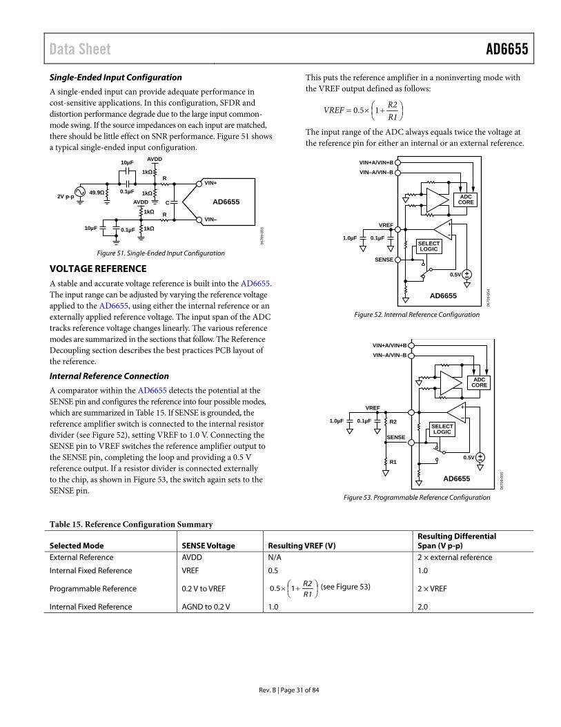
Internal Reference Connection
A comparator within the AD6655 detects the potential at the SENSE pin and configures the reference into four possible modes, which are summarized in Table 15. If SENSE is grounded, the reference amplifier switch is connected to the internal resistor divider (see Figure 52), setting VREF to 1.0 V. Connecting the SENSE pin to VREF switches the reference amplifier output to the SENSE pin, completing the loop and providing a 0.5 V reference output. If a resistor divider is connected externally to the chip, as shown in Figure 53, the switch again sets to the SENSE pin.
This puts the reference amplifier in a noninverting mode with the VREF output defined as follows:
+×=
R1R2VREF 15.0
The input range of the ADC always equals twice the voltage at the reference pin for either an internal or an external reference.
VREF
SENSE
0.5V
AD6655
SELECTLOGIC
0.1µF1.0µF
VIN–A/VIN–B
VIN+A/VIN+B
ADCCORE
0670
9-05
4
Figure 52. Internal Reference Configuration
0.5V
AD6655
SELECTLOGIC
VIN–A/VIN–B
VIN+A/VIN+B
ADCCORE
VREF
SENSE
0.1µF1.0µF R2
R1
0670
9-05
5
Figure 53. Programmable Reference Configuration
Table 15. Reference Configuration Summary
Selected Mode SENSE Voltage Resulting VREF (V) Resulting Differential Span (V p-p)
External Reference AVDD N/A 2 × external reference
Internal Fixed Reference VREF 0.5 1.0
Programmable Reference 0.2 V to VREF
+×
R1
R215.0 (see Figure 53) 2 × VREF
Internal Fixed Reference AGND to 0.2 V 1.0 2.0
AD6655 Data Sheet
Rev. B | Page 32 of 84
If the internal reference of the AD6655 is used to drive multiple converters to improve gain matching, the loading of the reference by the other converters must be considered. Figure 54 depicts how the internal reference voltage is affected by loading.
0
–1.250 2.0
LOAD CURRENT (mA)
REF
EREN
CE
VOLT
AG
E ER
RO
R (%
)
–0.25
–0.50
–0.75
–1.00
0.5 1.0 1.5
VREF = 0.5V
VREF = 1.0V
0670
9-05
6
Figure 54. VREF Accuracy vs. Load
External Reference Operation
The use of an external reference may be necessary to enhance the gain accuracy of the ADC or improve thermal drift charac-teristics. Figure 55 shows the typical drift characteristics of the internal reference in both 1.0 V and 0.5 V modes.
2.5
–2.5–40
TEMPERATURE (°C)
REF
EREN
CE
VOLT
AG
E ER
RO
R (m
V)
2.0
1.5
1.0
0.5
0
–0.5
–1.0
–1.5
–2.0
–20 0 20 40 60 80
0670
9-05
7
Figure 55. Typical VREF Drift
When the SENSE pin is tied to AVDD, the internal reference is disabled, allowing the use of an external reference. An internal reference buffer loads the external reference with an equivalent 6 kΩ load (see Figure 18). The internal buffer generates the positive and negative full-scale references for the ADC core. Therefore, the external reference must be limited to a maximum of 1.0 V.
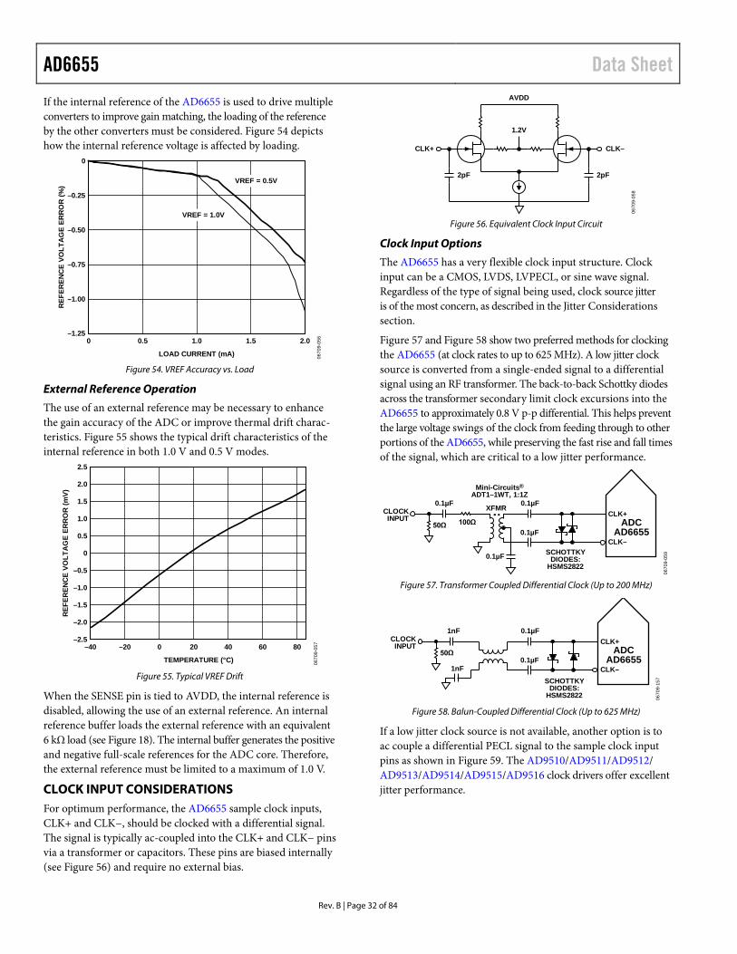
CLOCK INPUT CONSIDERATIONS For optimum performance, the AD6655 sample clock inputs, CLK+ and CLK−, should be clocked with a differential signal. The signal is typically ac-coupled into the CLK+ and CLK− pins via a transformer or capacitors. These pins are biased internally (see Figure 56) and require no external bias.
1.2V
AVDD
2pF 2pF
CLK–CLK+
0670
9-05
8
Figure 56. Equivalent Clock Input Circuit
Clock Input Options
The AD6655 has a very flexible clock input structure. Clock input can be a CMOS, LVDS, LVPECL, or sine wave signal. Regardless of the type of signal being used, clock source jitter is of the most concern, as described in the Jitter Considerations section.
Figure 57 and Figure 58 show two preferred methods for clocking the AD6655 (at clock rates to up to 625 MHz). A low jitter clock source is converted from a single-ended signal to a differential signal using an RF transformer. The back-to-back Schottky diodes across the transformer secondary limit clock excursions into the AD6655 to approximately 0.8 V p-p differential. This helps prevent the large voltage swings of the clock from feeding through to other portions of the AD6655, while preserving the fast rise and fall times of the signal, which are critical to a low jitter performance.
0.1µF
0.1µF
0.1µF0.1µF
SCHOTTKYDIODES:
HSMS2822
CLOCKINPUT
50Ω 100Ω
CLK–
CLK+ADC
AD6655
Mini-Circuits®ADT1–1WT, 1:1Z
XFMR
0670
9-05
9
Figure 57. Transformer Coupled Differential Clock (Up to 200 MHz)
0.1µF
0.1µF1nFCLOCKINPUT
1nF
50Ω
CLK–
CLK+ADC
AD6655
SCHOTTKYDIODES:
HSMS2822 0670
9-15
7
Figure 58. Balun-Coupled Differential Clock (Up to 625 MHz)
If a low jitter clock source is not available, another option is to ac couple a differential PECL signal to the sample clock input pins as shown in Figure 59. The AD9510/AD9511/AD9512/ AD9513/AD9514/AD9515/AD9516 clock drivers offer excellent jitter performance.
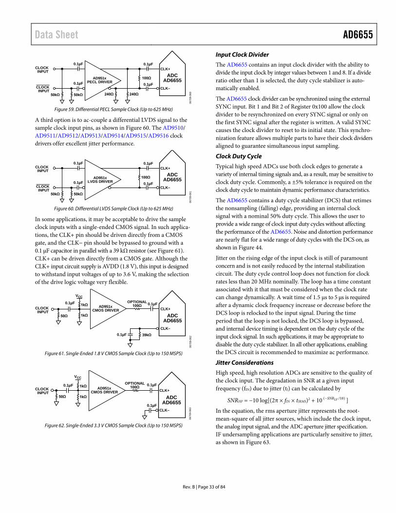
Data Sheet AD6655
Rev. B | Page 33 of 84
100Ω0.1µF
0.1µF0.1µF
0.1µF
240Ω240Ω
AD951xPECL DRIVER
50kΩ 50kΩCLK–
CLK+
ADCAD6655
CLOCKINPUT
CLOCKINPUT
0670
9-06
0
Figure 59. Differential PECL Sample Clock (Up to 625 MHz)
A third option is to ac-couple a differential LVDS signal to the sample clock input pins, as shown in Figure 60. The AD9510/ AD9511/AD9512/AD9513/AD9514/AD9515/AD9516 clock drivers offer excellent jitter performance.
100Ω0.1µF
0.1µF0.1µF
0.1µF
50kΩ 50kΩCLK–
CLK+
ADCAD6655
CLOCKINPUT
CLOCKINPUT
AD951xLVDS DRIVER
0670
9-06
1
Figure 60. Differential LVDS Sample Clock (Up to 625 MHz)
In some applications, it may be acceptable to drive the sample clock inputs with a single-ended CMOS signal. In such applica-tions, the CLK+ pin should be driven directly from a CMOS gate, and the CLK− pin should be bypassed to ground with a 0.1 µF capacitor in parallel with a 39 kΩ resistor (see Figure 61). CLK+ can be driven directly from a CMOS gate. Although the CLK+ input circuit supply is AVDD (1.8 V), this input is designed to withstand input voltages of up to 3.6 V, making the selection of the drive logic voltage very flexible.
OPTIONAL100Ω 0.1µF
0.1µF
0.1µF
39kΩ
50Ω
CLK–
CLK+
ADCAD6655
VCC
1kΩ
1kΩ
CLOCKINPUT
AD951xCMOS DRIVER
0670
9-06
2
Figure 61. Single-Ended 1.8 V CMOS Sample Clock (Up to 150 MSPS)
OPTIONAL100Ω 0.1µF
0.1µF
0.1µF
VCC
50Ω
CLK–
CLK+
ADCAD6655
1kΩ
1kΩ
CLOCKINPUT
AD951xCMOS DRIVER
0670
9-06
3
Figure 62. Single-Ended 3.3 V CMOS Sample Clock (Up to 150 MSPS)
Input Clock Divider
The AD6655 contains an input clock divider with the ability to divide the input clock by integer values between 1 and 8. If a divide ratio other than 1 is selected, the duty cycle stabilizer is auto-matically enabled.
The AD6655 clock divider can be synchronized using the external SYNC input. Bit 1 and Bit 2 of Register 0x100 allow the clock divider to be resynchronized on every SYNC signal or only on the first SYNC signal after the register is written. A valid SYNC causes the clock divider to reset to its initial state. This synchro-nization feature allows multiple parts to have their clock dividers aligned to guarantee simultaneous input sampling.
Clock Duty Cycle
Typical high speed ADCs use both clock edges to generate a variety of internal timing signals and, as a result, may be sensitive to clock duty cycle. Commonly, a ±5% tolerance is required on the clock duty cycle to maintain dynamic performance characteristics.
The AD6655 contains a duty cycle stabilizer (DCS) that retimes the nonsampling (falling) edge, providing an internal clock signal with a nominal 50% duty cycle. This allows the user to provide a wide range of clock input duty cycles without affecting the performance of the AD6655. Noise and distortion performance are nearly flat for a wide range of duty cycles with the DCS on, as shown in Figure 44.
Jitter on the rising edge of the input clock is still of paramount concern and is not easily reduced by the internal stabilization circuit. The duty cycle control loop does not function for clock rates less than 20 MHz nominally. The loop has a time constant associated with it that must be considered when the clock rate can change dynamically. A wait time of 1.5 µs to 5 µs is required after a dynamic clock frequency increase or decrease before the DCS loop is relocked to the input signal. During the time period that the loop is not locked, the DCS loop is bypassed, and internal device timing is dependent on the duty cycle of the input clock signal. In such applications, it may be appropriate to disable the duty cycle stabilizer. In all other applications, enabling the DCS circuit is recommended to maximize ac performance.
Jitter Considerations
High speed, high resolution ADCs are sensitive to the quality of the clock input. The degradation in SNR at a given input frequency (fIN) due to jitter (tJ) can be calculated by
SNRHF = −10 log[(2π × fIN × tJRMS)2 + 10 )10/( LFSNR/ ]
In the equation, the rms aperture jitter represents the root-mean-square of all jitter sources, which include the clock input, the analog input signal, and the ADC aperture jitter specification. IF undersampling applications are particularly sensitive to jitter, as shown in Figure 63.

AD6655 Data Sheet
Rev. B | Page 34 of 84
75
70
65
60
55
50
451 10 100 1000
SNR
(dB
c)
INPUT FREQUENCY (MHz)
3.00ps
0.05ps
0.20ps
0.50ps
1.00ps
1.50ps
2.00ps2.50ps
MEASURED
0670
9-06
4
Figure 63. SNR vs. Input Frequency and Jitter
The clock input should be treated as an analog signal in cases where aperture jitter may affect the dynamic range of the AD6655. Power supplies for clock drivers should be separated from the ADC output driver supplies to avoid modulating the clock signal with digital noise. Low jitter, crystal-controlled oscillators make the best clock sources. If the clock is generated from another type of source (by gating, dividing, or another method), it should be retimed by the original clock at the last step.
Refer to Application Note AN-501 and Application Note AN-756 for more information about jitter performance as it relates to ADCs (see www.analog.com).
POWER DISSIPATION AND STANDBY MODE As shown in Figure 64 through Figure 67, the power dissipated by the AD6655 is proportional to its sample rate. In CMOS output mode, the digital power dissipation is determined primarily by the strength of the digital drivers and the load on each output bit. The maximum DRVDD current (IDRVDD) can be calculated by
IDRVDD = VDRVDD × CLOAD × fCLK × N
where N is the number of output bits (30, in the case of the AD6655, assuming the FD bits are inactive).
This maximum current occurs when every output bit switches on every clock cycle, that is, a full-scale square wave at the Nyquist frequency of fCLK/2. In practice, the DRVDD current is established by the average number of output bits switching, which is determined by the sample rate and the characteristics of the analog input signal. Reducing the capacitive load presented to the output drivers can minimize digital power consumption. The data in Figure 64 through Figure 67 was taken using the same operating conditions as those used for the Typical Performance Characteristics, with a 5 pF load on each output driver.
1.50
1.25
1.00
0.75
0.50
0.25
0
0.6
IAVDD
IDVDD
IDRVDD
0.5
0.4
0.3
0.2
0.1
00 50 100
TOTA
L PO
WER
(W)
SUPP
LY C
UR
REN
T (A
)
15025 75 125SAMPLE RATE (MSPS)
TOTAL POWER
0670
9-06
5
Figure 64. AD6655-150 Power and Current vs. Sample Rate
1.50
1.25
1.00
0.75
0.50
0.25
0
0.6
0.5
IAVDD
IDVDD
IDRVDD
0.4
0.3
0.2
0.1
00 75
TOTA
L PO
WER
(W)
SUPP
LY C
UR
REN
T (A
)
25 50 125100SAMPLE RATE (MSPS)
TOTAL POWER
0670
9-16
6
Figure 65. AD6655-125 Power and Current vs. Sample Rate
1.25
1.00
0.75
0.50
0.25
0
0.5
0.4
IAVDD
IDVDD
IDRVDD
0.3
0.2
0.1
00 75
TOTA
L PO
WER
(W)
SUPP
LY C
UR
REN
T (A
)
25 50 100SAMPLE RATE (MSPS)
TOTAL POWER
0670
9-16
7
Figure 66. AD6655-105 Power and Current vs. Sample Rate

Data Sheet AD6655
Rev. B | Page 35 of 84
1.00
0.75
0.50
0.25
0
0.4
IAVDD
IDVDD
IDRVDD
0.3
0.2
0.1
00 60
TOTA
L PO
WER
(W)
SUPP
LY C
UR
REN
T (A
)
20 40 80SAMPLE RATE (MSPS)
TOTAL POWER
0670
9-16
8
Figure 67. AD6655-80 Power and Current vs. Sample Rate
By asserting PDWN (either through the SPI port or by asserting the PDWN pin high), the AD6655 is placed in power-down mode. In this state, the ADC typically dissipates 2.5 mW. During power-down, the output drivers are placed in a high impedance state. Asserting the PDWN pin low returns the AD6655 to its normal operating mode. Note that PDWN is referenced to the digital output driver supply (DRVDD) and should not exceed that supply voltage. PDWN can be driven with 1.8 V logic, even when DRVDD is at 3.3 V.
Low power dissipation in power-down mode is achieved by shutting down the reference, reference buffer, biasing networks, and clock. Internal capacitors are discharged when entering power-down mode and then must be recharged when returning to normal operation. As a result, wake-up time is related to the time spent in power-down mode, and shorter power-down cycles result in proportionally shorter wake-up times.
When using the SPI port interface, the user can place the ADC in power-down mode or standby mode. Standby mode allows the user to keep the internal reference circuitry powered when faster wake-up times are required. See the Memory Map Register Description section and Application Note AN-877, Interfacing to High Speed ADCs via SPI at www.analog.com for additional details.
DIGITAL OUTPUTS The AD6655 output drivers can be configured to interface with 1.8 V to 3.3 V CMOS logic families by matching DRVDD to the digital supply of the interfaced logic. Alternatively, the AD6655 outputs can be configured for either ANSI LVDS or reduced drive LVDS using a 1.8 V DRVDD supply.
In CMOS output mode, the output drivers are sized to provide sufficient output current to drive a wide variety of logic families. However, large drive currents tend to cause current glitches on the supplies that may affect converter performance. Applica-
tions requiring the ADC to drive large capacitive loads or large fanouts may require external buffers or latches.
The output data format can be selected for either offset binary or twos complement by setting the SCLK/DFS pin when operating in the external pin mode (see Table 16). As detailed in Application Note AN-877, Interfacing to High Speed ADCs via SPI, the data format can be selected for offset binary, twos complement, or gray code when using the SPI control.
Table 16. SCLK/DFS Mode Selection (External Pin Mode) Voltage at Pin SCLK/DFS SDIO/DCS AGND (default) Offset binary DCS disabled AVDD Twos complement DCS enabled
Digital Output Enable Function (OEB)
The AD6655 has a flexible three-state ability for the digital output pins. The three-state mode is enabled using the SMI SDO/OEB pin or through the SPI interface. If the SMI SDO/OEB pin is low, the output data drivers are enabled. If the SMI SDO/OEB pin is high, the output data drivers are placed in a high impedance state. This OEB function is not intended for rapid access to the data bus. Note that OEB is referenced to the digital output driver supply (DRVDD) and should not exceed that supply voltage. OEB can be driven with 1.8 V logic even when DRVDD is at 3.3 V.
When using the SPI interface, the data and fast detect outputs of each channel can be independently three-stated by using the output enable bar bit (Bit 4) in Register 0x14.
Interleaved CMOS Mode
Setting Bit 5 in Register 0x14 enables interleaved CMOS output mode. In this mode, output data is routed through Port A with the ADC Channel A output data present on the rising edge of DCO and the ADC Channel B output data present on the falling edge of DCO.
Timing
The AD6655 provides latched data with a pipeline delay that is dependent on which of the digital back end features are enabled. Data outputs are available one propagation delay (tPD) after the rising edge of the clock signal.
The length of the output data lines and loads placed on them should be minimized to reduce transients within the AD6655. These transients can degrade converter dynamic performance.
The lowest typical conversion rate of the AD6655 is 10 MSPS. At clock rates below 10 MSPS, dynamic performance may degrade.
Data Clock Output (DCO)
The AD6655 also provides data clock output (DCO) intended for capturing the data in an external register. Figure 2 through Figure 6 show a graphical timing description of the AD6655 output modes.

AD6655 Data Sheet
Rev. B | Page 36 of 84
Table 17. Output Data Format Input (V) Condition (V) Offset Binary Output Mode Twos Complement Mode OR VIN+ – VIN– < –VREF – 0.5 LSB 00 0000 0000 0000 10 0000 0000 0000 1 VIN+ – VIN– = –VREF 00 0000 0000 0000 10 0000 0000 0000 0 VIN+ – VIN– = 0 10 0000 0000 0000 00 0000 0000 0000 0 VIN+ – VIN– = +VREF – 1.0 LSB 11 1111 1111 1111 01 1111 1111 1111 0 VIN+ – VIN– > +VREF – 0.5 LSB 11 1111 1111 1111 01 1111 1111 1111 1
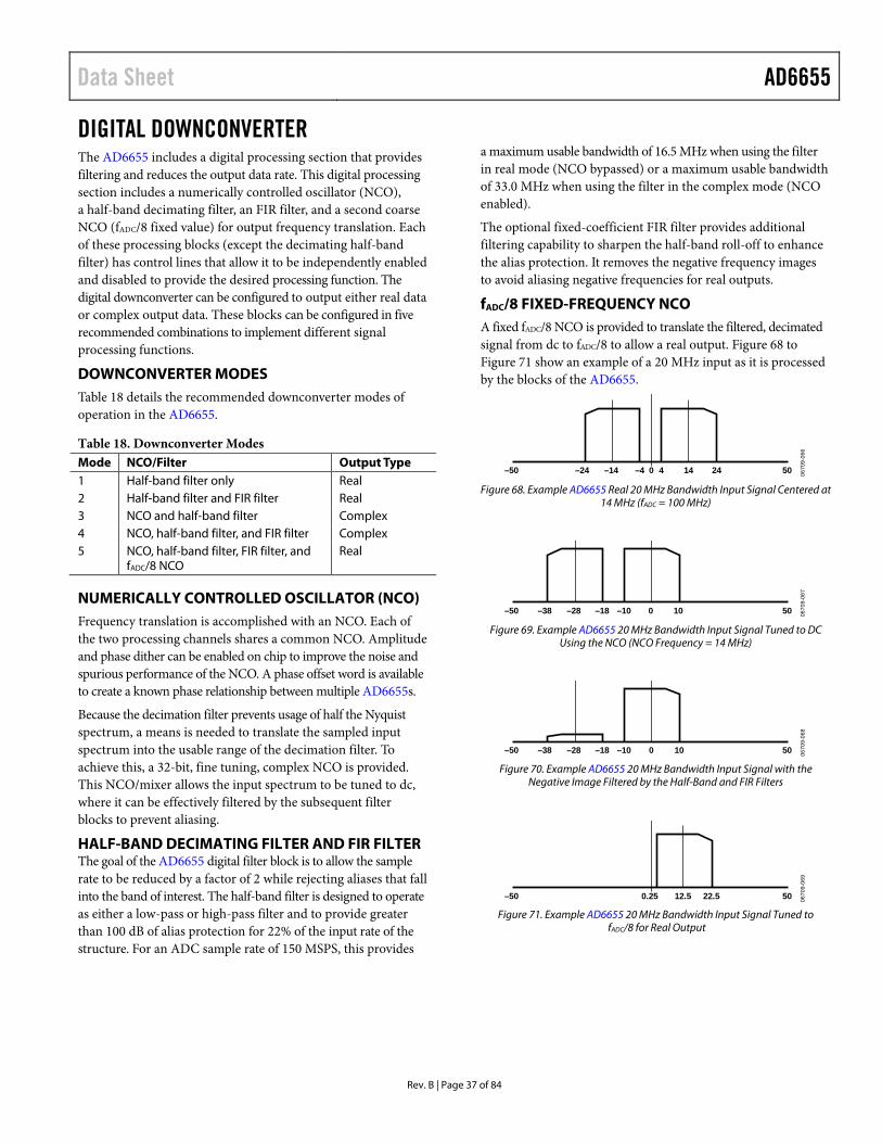
Data Sheet AD6655
Rev. B | Page 37 of 84
DIGITAL DOWNCONVERTER The AD6655 includes a digital processing section that provides filtering and reduces the output data rate. This digital processing section includes a numerically controlled oscillator (NCO), a half-band decimating filter, an FIR filter, and a second coarse NCO (fADC/8 fixed value) for output frequency translation. Each of these processing blocks (except the decimating half-band filter) has control lines that allow it to be independently enabled and disabled to provide the desired processing function. The digital downconverter can be configured to output either real data or complex output data. These blocks can be configured in five recommended combinations to implement different signal processing functions.
DOWNCONVERTER MODES Table 18 details the recommended downconverter modes of operation in the AD6655.
Table 18. Downconverter Modes Mode NCO/Filter Output Type 1 Half-band filter only Real 2 Half-band filter and FIR filter Real 3 NCO and half-band filter Complex 4 NCO, half-band filter, and FIR filter Complex 5 NCO, half-band filter, FIR filter, and
fADC/8 NCO Real
NUMERICALLY CONTROLLED OSCILLATOR (NCO) Frequency translation is accomplished with an NCO. Each of the two processing channels shares a common NCO. Amplitude and phase dither can be enabled on chip to improve the noise and spurious performance of the NCO. A phase offset word is available to create a known phase relationship between multiple AD6655s.
Because the decimation filter prevents usage of half the Nyquist spectrum, a means is needed to translate the sampled input spectrum into the usable range of the decimation filter. To achieve this, a 32-bit, fine tuning, complex NCO is provided. This NCO/mixer allows the input spectrum to be tuned to dc, where it can be effectively filtered by the subsequent filter blocks to prevent aliasing.
HALF-BAND DECIMATING FILTER AND FIR FILTER The goal of the AD6655 digital filter block is to allow the sample rate to be reduced by a factor of 2 while rejecting aliases that fall into the band of interest. The half-band filter is designed to operate as either a low-pass or high-pass filter and to provide greater than 100 dB of alias protection for 22% of the input rate of the structure. For an ADC sample rate of 150 MSPS, this provides
a maximum usable bandwidth of 16.5 MHz when using the filter in real mode (NCO bypassed) or a maximum usable bandwidth of 33.0 MHz when using the filter in the complex mode (NCO enabled).
The optional fixed-coefficient FIR filter provides additional filtering capability to sharpen the half-band roll-off to enhance the alias protection. It removes the negative frequency images to avoid aliasing negative frequencies for real outputs.
fADC/8 FIXED-FREQUENCY NCO A fixed fADC/8 NCO is provided to translate the filtered, decimated signal from dc to fADC/8 to allow a real output. Figure 68 to Figure 71 show an example of a 20 MHz input as it is processed by the blocks of the AD6655.
–50 –24 –14 14 24 50–4 40 0670
9-06
6
Figure 68. Example AD6655 Real 20 MHz Bandwidth Input Signal Centered at
14 MHz (fADC = 100 MHz)
–50 –38 –28 0 10 50–18 –10 0670
9-06
7
Figure 69. Example AD6655 20 MHz Bandwidth Input Signal Tuned to DC
Using the NCO (NCO Frequency = 14 MHz)
–50 –38 –28 0 10 50–18 –10 0670
9-06
8
Figure 70. Example AD6655 20 MHz Bandwidth Input Signal with the
Negative Image Filtered by the Half-Band and FIR Filters
–50 0.25 22.512.5 50 0670
9-06
9
Figure 71. Example AD6655 20 MHz Bandwidth Input Signal Tuned to
fADC/8 for Real Output
AD6655 Data Sheet
Rev. B | Page 38 of 84
NUMERICALLY CONTROLLED OSCILLATOR (NCO) FREQUENCY TRANSLATION This processing stage comprises a digital tuner consisting of a 32-bit complex numerically controlled oscillator (NCO). The two channels of the AD6655 share a single NCO. The NCO is optional and can be bypassed by clearing Bit 0 of Register 0x11D. This NCO block accepts a real input from the ADC stage and outputs a frequency translated complex (I and Q) output.
The NCO frequency is programmed in Register 0x11E, Register 0x11F, Register 0x120, and Register 0x121. These four 8-bit registers make up a 32-bit unsigned frequency programming word. Frequencies between −CLK/2 and +CLK/2 are represented using the following frequency words:
0x8000 0000 represents a frequency given by −CLK/2. 0x0000 0000 represents dc (frequency = 0 Hz). 0x7FFF FFFF represents CLK/2 − CLK/232.
Use the following equation to calculate the NCO frequency:
CLK
CLK
fffMod
NCO_FREQ),(
232
where: NCO_FREQ is a 32-bit twos complement number representing the NCO frequency register. f is the desired carrier frequency in hertz (Hz). fCLK is the AD6655 ADC clock rate in hertz (Hz).
NCO SYNCHRONIZATION The AD6655 NCOs within a single part or across multiple parts can be synchronized using the external SYNC input. Bit 3 and Bit 4 of Register 0x100 allow the NCO to be resynchronized on every SYNC signal or only on the first SYNC signal after the register is written. A valid SYNC causes the NCO to restart at the programmed phase offset value.
PHASE OFFSET The NCO phase offset register at Address 0x122 and Address 0x123 adds a programmable offset to the phase accumulator of the NCO. This 16-bit register is interpreted as a 16-bit unsigned integer. A 0x00 in this register corresponds to no offset, and a 0xFFFF corresponds to an offset of 359.995°. Each bit represents a phase change of 0.005°. This register allows multiple NCOs to be synchronized to produce outputs with predictable phase differences. Use the following equation to calculate the NCO phase offset value:
NCO_PHASE = 216 × PHASE/360
where: NCO_PHASE is a decimal number equal to the 16-bit binary number to be programmed at Register 0x122 and Register 0x123. PHASE is the desired NCO phase in degrees.
NCO AMPLITUDE AND PHASE DITHER The NCO block contains amplitude and phase dither to improve the spurious performance. Amplitude dither improves perfor-mance by randomizing the amplitude quantization errors within the angular-to-Cartesian conversion of the NCO. This option reduces spurs at the expense of a slightly raised noise floor. With amplitude dither enabled, the NCO has an SNR of >93 dB and an SFDR of >115 dB. With amplitude dither disabled, the SNR is increased to >96 dB at the cost of SFDR performance, which is reduced to 100 dB. The NCO amplitude dither is recommended and is enabled by setting Bit 1 of Register 0x11D.

Data Sheet AD6655
Rev. B | Page 39 of 84
DECIMATING HALF-BAND FILTER AND FIR FILTER The goal of the AD6655 half-band digital filter is to allow the sample rate to be reduced by a factor of 2 while rejecting aliases that fall into the band of interest. This filter is designed to operate as either a low-pass or a high-pass filter and to provide >100 dB of alias protection for 11% of the input rate of the structure. Used in conjunction with the NCO and the FIR filter, the half-band filter can provide an effective band-pass. For an ADC sample rate of 150 MSPS, this provides a maximum usable bandwidth of 33 MHz.
HALF-BAND FILTER COEFFICIENTS The 19-tap, symmetrical, fixed-coefficient half-band filter has low power consumption due to its polyphase implementation. Table 19 lists the coefficients of the half-band filter. The normalized coefficients used in the implementation and the decimal equivalent value of the coefficients are also listed. Coefficients not listed in Table 19 are 0s.
Table 19. Fixed Coefficients for Half-Band Filter Coefficient Number
Normalized Coefficient
Decimal Coefficient (20-Bit)
C0, C18 0.0008049 844 C2, C16 −0.0059023 −6189 C4, C14 0.0239182 25080 C6, C12 −0.0755024 −79170 C8, C10 0.3066864 321584 C9 0.5 524287
HALF-BAND FILTER FEATURES In the AD6655, the half-band filter cannot be disabled. The filter can be set for a low-pass or high-pass response. For a high-pass filter, Bit 1 of Register 0x103 should be set; for a low-pass response, this bit should be cleared. The low-pass response of the filter with respect to the normalized output rate is shown in Figure 72, and the high-pass response is shown in Figure 73.
0
–110
–100
–90
–80
–70
–60
–50
–40
–30
–20
–10
0 0.1 0.2 0.3 0.4
AM
PLIT
UD
E (d
Bc)
FRACTION OF INPUT SAMPLE RATE 0670
9-07
0
Figure 72. Half-Band Filter Low-Pass Response
0
–110
–100
–90
–80
–70
–60
–50
–40
–30
–20
–10
0 0.1 0.2 0.3 0.4
AM
PLIT
UD
E (d
Bc)
FRACTION OF INPUT SAMPLE RATE 0670
9-07
1
Figure 73. Half-Band Filter High-Pass Response
The half-band filter has a ripple of 0.000182 dB and a rejection of 100 dB. For an alias rejection of 100 dB, the alias protected bandwidth is 11% of the input sample rate. If both the I and the Q paths are used, a complex bandwidth of 22% of the input rate is available.
In the event of even Nyquist zone sampling, the half-band filter can be configured to provide a spectral reversal. Setting Bit 2 high in Address 0x103 enables the spectral reversal feature.
The half-band decimation phase can be selected such that the half-band filter starts on the first or second sample following synchronization. This shifts the output from the half-band between the two input sample clocks. The decimation phase can be set to 0 or 1, using Bit 3 of Register 0x103.
FIXED-COEFFICIENT FIR FILTER Following the half-band filters is a 66-tap, fixed-coefficient FIR filter. This filter is useful in providing extra alias protection for the decimating half-band filter. It is a simple sum-of-products FIR filter with 66 filter taps and 21-bit fixed coefficients. Note that this filter does not decimate. The normalized coefficients used in the implementation and the decimal equivalent value of the coefficients are listed in Table 20.
The user can either select or bypass this filter, but the FIR filter can be enabled only when the half-band filter is enabled. Writing Logic 0 to the enable FIR filter bit (Bit 0) in Register 0x102 bypasses this fixed-coefficient filter. The filter is necessary when using the final NCO with a real output; bypassing it when using other configurations results in power savings.

AD6655 Data Sheet
Rev. B | Page 40 of 84
Table 20. FIR Filter Coefficients Coefficient Number
Normalized Coefficient
Decimal Coefficient (21-Bit)
C0, C65 0.0001826 383 C1, C64 0.0006824 1431 C2, C63 0.0009298 1950 C3, C62 0.0000458 96 C4, C61 −0.0012689 −2661 C5, C60 −0.0008345 −1750 C6, C59 0.0011806 2476 C7, C58 0.0011387 2388 C8, C57 −0.0018439 −3867 C9, C56 −0.0024557 −5150 C10, C55 0.0018063 3788 C11, C54 0.0035825 7513 C12, C53 −0.0021510 −4511 C13, C52 −0.0056810 −11914 C14, C51 0.0017405 3650 C15, C50 0.0078602 16484 C16, C49 −0.0013437 −2818 C17, C48 −0.0110626 −23200 C18, C47 −0.0000229 −48 C19, C46 0.0146618 30748 C20, C45 0.0018959 3976 C21, C44 −0.0195594 −41019 C22, C43 −0.0053153 −11147 C23, C42 0.0255623 53608 C24, C41 0.0104036 21818 C25, C40 −0.0341468 −71611 C26, C39 −0.0192165 −40300 C27, C38 0.0471258 98830 C28, C37 0.0354118 74264 C29, C36 −0.0728111 −152696 C30, C35 −0.0768890 −161248 C31, C34 0.1607208 337056 C32, C33 0.4396725 922060
SYNCHRONIZATION The AD6655 half-band filters within a single part or across multiple parts can be synchronized using the external SYNC input. Bit 5 and Bit 6 of Register 0x100 allow the half-bands to be resynchronized on every SYNC signal or only on the first SYNC signal after the register is written. A valid SYNC causes the half-band filter to restart at the programmed decimation phase value.
COMBINED FILTER PERFORMANCE The combined response of the half-band filter and the FIR filter is shown in Figure 74. The act of bandlimiting the ADC data with the half-band filter ideally provides a 3 dB improvement in the SNR at the expense of the sample rate and available bandwidth of the output data. As a consequence of finite math, additional quantization noise is added to the system due to truncation in the NCO and half-band. As a consequence of the digital filter rejection of out-of-band noise (assuming no quantization in the filters and with a white noise floor from the ADC), there should be a 3.16 dB improvement in the ADC SNR. However, the added quantization lessens improvement to about 2.66 dB.
0
–110
–100
–90
–80
–70
–60
–50
–40
–30
–20
–10
0 0.1 0.2 0.3 0.4
AM
PLIT
UD
E (d
Bc)
FRACTION OF INPUT SAMPLE RATE 0670
9-07
2
Figure 74. Half-Band Filter and FIR Filter Composite Response
FINAL NCO The output of the 32-bit fine tuning NCO is complex and typically centered in frequency around dc. This complex output is carried through the stages of the half-band and FIR filters to provide proper antialiasing filtering. The final NCO provides a means to move this complex output signal away from dc so that a real output can be provided from the AD6655. The final NCO, if enabled, translates the output from dc to a frequency equal to the ADC sampling frequency divided by 8 (fADC/8). This provides the user a decimated output signal centered at fADC/8 in frequency. Optionally, this final NCO can be bypassed, and the dc-centered I and Q values can be output in an interleaved fashion.

Data Sheet AD6655
Rev. B | Page 41 of 84
ADC OVERRANGE AND GAIN CONTROL In receiver applications, it is desirable to have a mechanism to reliably determine when the converter is about to be clipped. The standard overflow indicator provides after-the-fact infor-mation on the state of the analog input that is of limited usefulness. Therefore, it is helpful to have a programmable threshold below full scale that allows time to reduce the gain before the clip actually occurs. In addition, because input signals can have significant slew rates, latency of this function is of major concern. Highly pipelined converters can have significant latency. A good compro-mise is to use the output bits from the first stage of the ADC for this function. Latency for these output bits is very low, and overall resolution is not highly significant. Peak input signals are typically between full scale and 6 dB to 10 dB below full scale. A 3-bit or 4-bit output provides adequate range and resolution for this function.
Using the SPI port, the user can provide a threshold above which an overrange output is active. As long as the signal is below that threshold, the output should remain low. The fast detect outputs can also be programmed via the SPI port so that one of the pins functions as a traditional overrange pin for customers who currently use this feature. In this mode, all 14 bits of the converter are examined in the traditional manner, and the output is high for the condition normally defined as overflow. In either mode, the magnitude of the data is considered in the calculation of the condition (but the sign of the data is not considered). The threshold detection responds identically to positive and negative signals outside the desired range (magnitude).
FAST DETECT OVERVIEW The AD6655 contains circuitry to facilitate fast overrange detection, allowing very flexible external gain control imple-mentations. Each ADC has four fast detect (FD) output pins that are used to output information about the current state of the ADC input level. The function of these pins is programmable via the fast detect mode select bits and the fast detect enable bit in Register 0x104, allowing range information to be output from several points in the internal data path. These output pins can also be set up to indicate the presence of overrange or underrange conditions, according to programmable threshold levels. Table 21 shows the six configurations available for the fast detect pins.
Table 21. Fast Detect Mode Select Bits Settings
Fast Detect Mode Select bits (Register 0x104[3:1])
Information Presented on Fast Detect (FD) Pins of Each ADC1, 2 FD[3] FD[2] FD[1] FD[0]
000 ADC fast magnitude (see Table 22) 001 ADC fast magnitude
(see Table 23) OR
010 ADC fast magnitude
(see Table 24)
OR F_LT
011 ADC fast magnitude
(see Table 24)
C_UT F_LT
100 OR C_UT F_UT F_LT 101 OR F_UT IG DG 1 The fast detect pins are FD0A/FD0B to FD3A/FD3B for the CMOS mode
configuration and FD0+/FD0− to FD3+/FD3− for the LVDS mode configuration.
2 See the ADC Overrange (OR) and Gain Switching sections for more information about OR, C_UT, F_UT, F_LT, IG, and DG.
ADC FAST MAGNITUDE When the fast detect output pins are configured to output the ADC fast magnitude (that is, when the fast detect mode select bits are set to 0b000), the information presented is the ADC level from an early converter stage with a latency of only two clock cycles in CMOS output modes. In LVDS output mode, the fast detect bits have a latency of six cycles in all fast detect modes. Using the fast detect output pins in this configuration provides the earliest possible level indication information. Because this information is provided early in the datapath, there is signifi-cant uncertainty in the level indicated. The nominal levels, along with the uncertainty indicated by the ADC fast magnitude, are shown in Table 22. Because the DCO is at one-half the sample rate, the user can obtain all the fast detect information by sampling the fast detect outputs on both the rising and falling edge of DCO (see Figure 2 for timing information).
Table 22. ADC Fast Magnitude Nominal Levels with Fast Detect Mode Select Bits = 000 ADC Fast Magnitude on FD[3:0] Pins
Nominal Input Magnitude Below FS (dB)
Nominal Input Magnitude Uncertainty (dB)
0000 <−24 Minimum to −18.07 0001 −24 to −14.5 −30.14 to −12.04 0010 −14.5 to −10 −18.07 to −8.52 0011 −10 to −7 −12.04 to −6.02 0100 −7 to −5 −8.52 to −4.08 0101 −5 to −3.25 −6.02 to −2.5 0110 −3.25 to −1.8 −4.08 to −1.16 0111 −1.8 to −0.56 −2.5 to FS 1000 −0.56 to 0 −1.16 to 0

AD6655 Data Sheet
Rev. B | Page 42 of 84
When the fast detect mode select bits are set to 0b001, 0b010, or 0b011, a subset of the fast detect output pins are available. In these modes, the fast detect output pins have a latency of six clock cycles, and the greater of the two input samples is output at the DCO rate. Table 23 shows the corresponding ADC input levels when the fast detect mode select bits are set to 0b001 (that is, when the ADC fast magnitude is presented on the FD[3:1] pins).
Table 23. ADC Fast Magnitude Nominal Levels with Fast Detect Mode Select Bits = 001 ADC Fast Magitude on FD[2:0] Pins
Nominal Input Magnitude Below FS (dB)
Nominal Input Magnitude Uncertainty (dB)
000 <−24 Minimum to −18.07 001 −24 to −14.5 −30.14 to −12.04 010 −14.5 to −10 −18.07 to −8.52 011 −10 to −7 −12.04 to −6.02 100 −7 to −5 −8.52 to −4.08 101 −5 to −3.25 −6.02 to −2.5 110 −3.25 to −1.8 −4.08 to −1.16 111 −1.8 to 0 −2.5 to 0
When the fast detect mode select bits are set to 0b010 or 0b011 (that is, when ADC fast magnitude is presented on the FD[2:1] pins), the LSB is not provided. The input ranges for this mode are shown in Table 24.
Table 24. ADC Fast Magnitude Nominal Levels with Fast Detect Mode Select Bits = 010 or 011 ADC Fast Magitude on FD[2:1] Pins
Nominal Input Magnitude Below FS (dB)
Nominal Input Magnitude Uncertainty (dB)
00 <−14.5 Minimum to −12.04 01 −14.5 to −7 −18.07 to −6.02 10 −7 to −3.25 −8.52 to −2.5 11 −3.25 to 0 −4.08 to 0
ADC OVERRANGE (OR) The ADC overrange indicator is asserted when an overrange is detected on the input of the ADC. The overrange condition is determined at the output of the ADC pipeline and, therefore, is subject to a latency of 12 ADC clock cycles. An overrange at the input is indicated by this bit 12 clock cycles after it occurs.
GAIN SWITCHING The AD6655 includes circuitry that is useful in applications either where large dynamic ranges exist or where gain ranging converters are employed. This circuitry allows digital thresholds to be set such that an upper threshold and a lower threshold can be programmed. Fast detect mode select bits = 010 through fast detect mode select bits = 101 support various combinations of the gain switching options.
One such use is to detect when an ADC is about to reach full scale with a particular input condition. The result is to provide an indicator that can be used to quickly insert an attenuator that prevents ADC overdrive.
Coarse Upper Threshold (C_UT)
The coarse upper threshold indicator is asserted if the ADC fast magnitude input level is greater than the level programmed in the coarse upper threshold register (Address 0x105[2:0]). This value is compared with the ADC Fast Magnitude Bits[2:0]. The coarse upper threshold output is output two clock cycles after the level is exceeded at the input and, therefore, provides a fast indication of the input signal level. The coarse upper threshold levels are shown in Table 25. This indicator remains asserted for a minimum of two ADC clock cycles or until the signal drops below the threshold level.
Table 25. Coarse Upper Threshold Levels
Coarse Upper Threshold Register[2:0]
C_UT Is Active When Signal Magnitude Below FS Is Greater Than (dB)
000 <−24 001 −24 010 −14.5 011 −10 100 −7 101 −5 110 −3.25 111 −1.8
Fine Upper Threshold (F_UT)
The fine upper threshold indicator is asserted if the input magnitude exceeds the value programmed in the fine upper threshold register located in Register 0x106 and Register 0x107. The 13-bit threshold register is compared with the signal magni-tude at the output of the ADC. This comparison is subject to the ADC clock latency but is accurate in terms of converter resolution. The fine upper threshold magnitude is defined by the following equation:
dBFS = 20 log(Threshold Magnitude/213)
Fine Lower Threshold (F_LT)
The fine lower threshold indicator is asserted if the input magni-tude is less than the value programmed in the fine lower threshold register located at Register 0x108 and Register 0x109. The fine lower threshold register is a 13-bit register that is compared with the signal magnitude at the output of the ADC. This comparison is subject to ADC clock latency but is accurate in terms of converter resolution. The fine lower threshold magnitude is defined by the following equation:
dBFS = 20 log(Threshold Magnitude/213)
The operation of the fine upper threshold and fine lower threshold indicators is shown in Figure 75.

Data Sheet AD6655
Rev. B | Page 43 of 84
Increment Gain (IG) and Decrement Gain (DG)
The increment gain and decrement gain indicators are intended to be used together to provide information to enable external gain control. The decrement gain indicator works in conjunction with the coarse upper threshold bits, asserting when the input magnitude is greater than the 3-bit value in the coarse upper threshold register (Address 0x105). The increment gain indicator, similarly, corresponds to the fine lower threshold bits except that it is asserted only if the input magnitude is less than the value programmed in the fine lower threshold register after the dwell time elapses. The dwell time is set by the 16-bit dwell time value located at Address 0x10A and Address 0x10B and is set in units of ADC input clock cycles ranging from 1 to 65,535. The fine lower threshold register is a 13-bit register that is compared
with the magnitude at the output of the ADC. This comparison is subject to the ADC clock latency but allows a finer, more accurate comparison. The fine upper threshold magnitude is defined by the following equation:
dBFS = 20 log(Threshold Magnitude/213)
The decrement gain output works from the ADC fast detect output pins, providing a fast indication of potential overrange conditions. The increment gain uses the comparison at the output of the ADC, requiring the input magnitude to remain below an accurate, programmable level for a predefined period before signaling external circuitry to increase the gain.
The operation of the increment gain output and decrement gain output is shown graphically in Figure 75.
UPPER THRESHOLD (COARSE OR FINE)
FINE LOWER THRESHOLD
IG
DG
F_LT
C_UT OR F_UT*
DWELL TIME
TIMER RESET BYRISE ABOVE F_LT
TIMER COMPLETES BEFORESIGNAL RISES ABOVE F_LT
NOTE: OUTPUTS FOLLOW THE INSTANTEOUS SIGNAL LEVEL AND NOT THE ENVELOPE BUT ARE GUARANTEED ACTIVE FOR A MINIMUM OF 2 ADC CLOCK CYCLES.*C_UT AND F_UT DIFFER ONLY IN ACCURACY AND LATENCY.
DWELL TIME
0670
9-07
3
Figure 75. Threshold Settings for C_UT, F_UT, F_LT, DG, and IG

AD6655 Data Sheet
Rev. B | Page 44 of 84
SIGNAL MONITOR The signal monitor block provides additional information about the signal being digitized by the ADC. The signal monitor computes the rms input magnitude, the peak magnitude, and/or the number of samples by which the magnitude exceeds a particular threshold. Together, these functions can be used to gain insight into the signal characteristics and to estimate the peak/average ratio or even the shape of the complementary cumulative distribution function (CCDF) curve of the input signal. This information can be used to drive an AGC loop to optimize the range of the ADC in the presence of real-world signals.
The signal monitor result values can be obtained from the part by reading back internal registers at Address 0x116 to Address 0x11B, using the SPI port or the signal monitor SPORT output. The output contents of the SPI-accessible signal monitor registers are set via the two signal monitor mode bits of the signal monitor control register (Address 0x112). Both ADC channels must be configured for the same signal monitor mode. Separate SPI-accessible, 20-bit signal monitor result (SMR) registers are provided for each ADC channel. Any combination of the signal monitor functions can also be output to the user via the serial SPORT interface. These outputs are enabled using the peak detector output enable, the rms magnitude output enable, and the threshold crossing output enable bits in the signal monitor SPORT control register (Address 0x1111).
For each signal monitor measurement, a programmable signal monitor period register (SMPR) controls the duration of the measurement. This time period is programmed as the number of input clock cycles in a 24-bit signal monitor period register located at Address 0x113, Address 0x114, and Address 0x115. This register can be programmed with a period from 128 samples to 16.78 (224) million samples.
Because the dc offset of the ADC can be significantly larger than the signal of interest (affecting the results from the signal monitor), a dc correction circuit is included as part of the signal monitor block to null the dc offset before measuring the power.
PEAK DETECTOR MODE The magnitude of the input port signal is monitored over a programmable time period (determined by SMPR) to give the peak value detected. This function is enabled by programming a Logic 1 in the signal monitor mode bits of the signal monitor control register or by setting the peak detector output enable bit in the signal monitor SPORT control register. The 24-bit SMPR must be programmed before activating this mode.
After enabling this mode, the value in the SMPR is loaded into a monitor period timer, and the countdown is started. The magnitude of the input signal is compared with the value in the internal peak level holding register (not accessible to the user), and the greater of the two is updated as the current peak level. The initial value of the peak level holding register is set to the
current ADC input signal magnitude. This comparison continues until the monitor period timer reaches a count of 1.
When the monitor period timer reaches a count of 1, the 13-bit peak level value is transferred to the signal monitor holding register (not accessible to the user), which can be read through the SPI port or output through the SPORT serial interface. The monitor period timer is reloaded with the value in the SMPR, and the countdown is restarted. In addition, the magnitude of the first input sample is updated in the peak level holding register, and the comparison and update procedure, as explained previously, continues.
Figure 76 is a block diagram of the peak detector logic. The SMR register contains the absolute magnitude of the peak detected by the peak detector logic.
POWER MONITORHOLDINGREGISTER
MAGNITUDESTORAGEREGISTER
COMPAREA>B
TOMEMORY
MAP
FROMMEMORY
MAP
FROMINPUTPORTS
LOAD
CLEAR
LOAD LOAD
TOINTERRUPT
CONTROLLERIS COUNT = 1?DOWN
COUNTERPOWER MONITORPERIOD REGISTER
0670
9-07
4
Figure 76. ADC Input Peak Detector Block Diagram
RMS/MS MAGNITUDE MODE In this mode, the root-mean-square (rms) or mean-square (ms) magnitude of the input port signal is integrated (by adding an accumulator) over a programmable time period (determined by SMPR) to give the rms or ms magnitude of the input signal. This mode is set by programming Logic 0 in the signal monitor mode bits of the signal monitor control register or by setting the rms magnitude output enable bit in the signal monitor SPORT control register. The 24-bit SMPR, representing the period over which integration is performed, must be programmed before activating this mode.
After enabling the rms/ms magnitude mode, the value in the SMPR is loaded into a monitor period timer, and the countdown is started immediately. Each input sample is converted to floating-point format and squared. It is then converted to 11-bit, fixed-point format and added to the contents of the 24-bit accumulator. The integration continues until the monitor period timer reaches a count of 1.
When the monitor period timer reaches a count of 1, the square root of the value in the accumulator is taken and transferred (after some formatting) to the signal monitor holding register, which can be read through the SPI port or output through the SPORT serial port. The monitor period timer is reloaded with the value in the SMPR, and the countdown is restarted.

Data Sheet AD6655
Rev. B | Page 45 of 84
In addition, the first input sample signal power is updated in the accumulator, and the accumulation continues with the subsequent input samples. Figure 77 illustrates the rms magnitude monitoring logic.
POWER MONITORHOLDINGREGISTER
ACCUMULATOR
FROMMEMORY
MAP
FROMINPUTPORTS
LOAD
CLEAR LOAD
IS COUNT = 1?DOWNCOUNTER
POWER MONITORPERIOD REGISTER
TOMEMORY
MAP
TOINTERRUPT
CONTROLLER
0670
9-07
5
Figure 77. ADC Input RMS Magnitude Monitoring Block Diagram
For rms magnitude mode, the value in the signal monitor result (SMR) register is a 20-bit fixed-point number. The following equation can be used to determine the rms magnitude in dBFS from the MAG value in the register. Note that if the signal monitor period (SMP) is a power of 2, the second term in the equation becomes 0.
RMS Magnitude = 20 log [ ]
/
)(log20 22log10
2 SMPceilSMPMAG
For ms magnitude mode, the value in the SMR is a 20-bit fixed-point number. The following equation can be used to determine the ms magnitude in dBFS from the MAG value in the register. Note that if the SMP is a power of 2, the second term in the equation becomes 0.
MS Magnitude = 10 log [ ]
/
)(log20 22log10
2 SMPceilSMPMAG
THRESHOLD CROSSING MODE In the threshold crossing mode of operation, the magnitude of the input port signal is monitored over a programmable time period (given by SMPR) to count the number of times it crosses a certain programmable threshold value. This mode is set by programming Logic 1x (where x is a don’t care bit) in the signal monitor mode bits of the signal monitor control register or by setting the threshold crossing output enable bit in the signal monitor SPORT control register. Before activating this mode, the user needs to program the 24-bit SMPR and the 13-bit upper threshold register for each individual input port. The same upper threshold register is used for both signal monitoring and gain control (see the ADC Overrange and Gain Control section).
After entering this mode, the value in the SMPR is loaded into a monitor period timer, and the countdown is started. The magnitude of the input signal is compared with the upper threshold register (programmed previously) on each input clock cycle. If the input signal has a magnitude greater than the upper threshold register, the internal count register is incremented by 1. The initial value of the internal count register is set to 0. This comparison and incrementing of the internal count register continues until the monitor period timer reaches a count of 1.
When the monitor period timer reaches a count of 1, the value in the internal count register is transferred to the signal monitor holding register, which can be read through the SPI port or output through the SPORT serial port.
The monitor period timer is reloaded with the value in the SMPR register, and the countdown is restarted. The internal count register is also cleared to a value of 0. Figure 78 illustrates the threshold crossing logic. The value in the SMR register is the number of samples that have a magnitude greater than the threshold register.
POWER MONITORHOLDINGREGISTER
COMPAREA>B
UPPERTHRESHOLDREGISTER
COMPAREA>B
FROMMEMORY
MAP
FROMMEMORY
MAP
FROMINPUTPORTS
LOAD
CLEAR LOAD
IS COUNT = 1?DOWNCOUNTER
POWER MONITORPERIOD REGISTER
B
A
TOMEMORY
MAP
TOINTERRUPT
CONTROLLER
0670
9-07
6
Figure 78. ADC Input Threshold Crossing Block Diagram
ADDITIONAL CONTROL BITS For additional flexibility in the signal monitoring process, two control bits are provided in the signal monitor control register. They are the signal monitor enable bit and the complex power calculation mode enable bit.
Signal Monitor Enable Bit
The signal monitor enable bit, located in Bit 0 of Register 0x112, enables operation of the signal monitor block. If the signal monitor function is not needed in a particular application, this bit should be cleared to conserve power.
Complex Power Calculation Mode Enable Bit
When this bit is set, the part assumes that Channel A is digitizing the I data and Channel B is digitizing the Q data for a complex input signal (or vice versa). In this mode, the power reported is equal to
22 QI +
This result is presented in the Signal Monitor DC Value Channel A register if the signal monitor mode bits are set to 00. The Signal Monitor DC Value Channel B register continues to compute the Channel B value.
DC CORRECTION Because the dc offset of the ADC may be significantly larger than the signal being measured, a dc correction circuit is included to null the dc offset before measuring the power. The dc correction circuit can also be switched into the main signal path, but this may not be appropriate if the ADC is digitizing a time-varying signal with significant dc content, such as GSM.
AD6655 Data Sheet
Rev. B | Page 46 of 84
DC Correction Bandwidth The dc correction circuit is a high-pass filter with a programmable bandwidth (ranging between 0.15 Hz and 1.2 kHz at 125 MSPS). The bandwidth is controlled by writing the 4-bit dc correction control register located at Register 0x10C, Bits[5:2]. The following equation can be used to compute the bandwidth value for the dc correction circuit:
π××= //
22__ 14k CLKf
BWCorrDC
where: k is the 4-bit value programmed in Bits[5:2] of Register 0x10C (values between 0 and 13 are valid for k; programming 14 or 15 provides the same result as programming 13). fCLK is the AD6655 ADC sample rate in hertz (Hz).
DC Correction Readback The current dc correction value can be read back in Register 0x10D and Register 0x10E for Channel A and Register 0x10F and Register 0x110 for Channel B. The dc correction value is a 14-bit value that can span the entire input range of the ADC.
DC Correction Freeze Setting Bit 6 of Register 0x10C freezes the DC correction at its current state and continues to use the last updated value as the dc correction value. Clearing this bit restarts dc correction and adds the currently calculated value to the data.
DC Correction Enable Bits
Setting Bit 0 of Register 0x10C enables dc correction for use in the signal monitor calculations. The calculated dc correction value can be added to the output data signal path by setting Bit 1 of Register 0x10C.
SIGNAL MONITOR SPORT OUTPUT The SPORT is a serial interface with three output pins: the SMI SCLK (SPORT clock), SMI SDFS (SPORT frame sync), and SMI SDO (SPORT data output). The SPORT is the master and drives all three SPORT output pins on the chip.
SMI SCLK
The data and frame sync are driven on the positive edge of the SMI SCLK. The SMI SCLK has three possible baud rates: 1/2, 1/4, or 1/8 the ADC clock rate, based on the SPORT controls. The SMI SCLK can also be gated off when not sending any data, based on the SPORT SMI SCLK sleep bit. Using this bit to disable the SMI SCLK when it is not needed can reduce any coupling errors back into the signal path, if these prove to be a problem in the system. Doing so, however, has the disadvantage of spreading the frequency content of the clock. If desired the SMI SCLK can be left running to ease frequency planning.
SMI SDFS
The SMI SDFS is the serial data frame sync, and it defines the start of a frame. One SPORT frame includes data from both datapaths. The data from Datapath A is sent just after the frame sync, followed by data from Datapath B.
SMI SDO
The SMI SDO is the serial data output of the block. The data is sent MSB first on the next positive edge after the SMI SDFS. Each data output block includes one or more of rms magnitude, peak level, and threshold crossing values from each datapath in the stated order. If enabled, the data is sent, rms first, followed by peak and threshold, as shown in Figure 79.
20 CYCLES 16 CYCLES16 CYCLES 20 CYCLES 16 CYCLES 16 CYCLES
SMI SDFS
MSB MSBRMS/MS CH A PK CH A PK CH B THR CH BRMS/MS CH B RMS/MS CH ALSB LSBTHR CH ASMI SDO
SMI SCLK
GATED, BASED ON CONTROL
0670
9-07
7
Figure 79. Signal Monitor SPORT Output Timing (RMS, Peak, and Threshold Enabled)
20 CYCLES 16 CYCLES 20 CYCLES 16 CYCLES
SMI SCLK
SMI SDFS
SMI SDO MSB MSBRMS/MS CH A RMS/MS CH ALSB THR CH A RMS/MS CH B LSB THR CH B
GATED, BASED ON CONTROL
0670
9-07
8
Figure 80. Signal Monitor SPORT Output Timing (RMS and Threshold Enabled)
Data Sheet AD6655
Rev. B | Page 47 of 84
CHANNEL/CHIP SYNCHRONIZATION The AD6655 has a SYNC input that allows the user flexible synchronization options for synchronizing the internal blocks. The sync feature is useful for guaranteeing synchronized operation across multiple ADCs. The input clock divider, NCO, half-band filters, and signal monitor block can be synchronized using the SYNC input. Each of these blocks, except for the signal monitor, can be enabled to synchronize on a single occurrence of the SYNC signal or on every occurrence.
The SYNC input is internally synchronized to the sample clock. However, to ensure that there is no timing uncertainty between multiple parts, the SYNC input signal should be synchronized to the input clock signal. The SYNC input should be driven using a single-ended CMOS type signal.
AD6655 Data Sheet
Rev. B | Page 48 of 84
SERIAL PORT INTERFACE (SPI) The AD6655 serial port interface (SPI) allows the user to configure the converter for specific functions or operations through a structured register space provided inside the ADC. The SPI gives the user added flexibility and customization, depending on the application. Addresses are accessed via the serial port and can be written to or read from via the port. Memory is organized into bytes that can be further divided into fields. These fields are documented in the Memory Map section. For detailed operational information, see Application Note AN-877, Interfacing to High Speed ADCs via SPI.
CONFIGURATION USING THE SPI Three pins define the SPI of this ADC: the SCLK/DFS pin, the SDIO/DCS pin, and the CSB pin (see Table 26). The SCLK/DFS (serial clock) pin is used to synchronize the read and write data presented from/to the ADC. The SDIO/DCS (serial data input/ output) pin is a dual-purpose pin that allows data to be sent and read from the internal ADC memory map registers. The CSB (chip select bar) pin is an active-low control that enables or disables the read and write cycles.
Table 26. Serial Port Interface Pins Pin Function SCLK Serial Clock. The serial shift clock input, which is used to
synchronize serial interface reads and writes. SDIO Serial Data Input/Output. A dual-purpose pin that
typically serves as an input or an output, depending on the instruction being sent and the relative position in the timing frame.
CSB Chip Select Bar. An active-low control that gates the read and write cycles.
The falling edge of the CSB, in conjunction with the rising edge of the SCLK, determines the start of the framing. An example of the serial timing and its definitions can be found in Figure 81 and Table 9.
Other modes involving the CSB are available. The CSB can be held low indefinitely, which permanently enables the device; this is called streaming. The CSB can stall high between bytes to allow for additional external timing. When CSB is tied high, SPI functions are placed in a high impedance mode. This mode turns on any SPI pin secondary functions.
During an instruction phase, a 16-bit instruction is transmitted. Data follows the instruction phase, and its length is determined by the W0 bit and the W1 bit.
All data is composed of 8-bit words. The first bit of each individual byte of serial data indicates whether a read command or a write command is issued. This allows the serial data input/output (SDIO) pin to change direction from an input to an output.
In addition to word length, the instruction phase determines whether the serial frame is a read or write operation, allowing the serial port to be used both to program the chip and to read the contents of the on-chip memory. If the instruction is a readback operation, performing a readback causes the serial data input/ output (SDIO) pin to change direction from an input to an output at the appropriate point in the serial frame.
Data can be sent in MSB-first mode or in LSB-first mode. MSB first is the default on power-up and can be changed via the SPI port configuration register. For more information about this and other features, see Application Note AN-877, Interfacing to High Speed ADCs via SPI at www.analog.com.
HARDWARE INTERFACE The pins described in Table 26 comprise the physical interface between the user programming device and the serial port of the AD6655. The SCLK pin and the CSB pin function as inputs when using the SPI interface. The SDIO pin is bidirectional, functioning as an input during write phases and as an output during readback.
The SPI interface is flexible enough to be controlled by either FPGAs or microcontrollers. One method for SPI configuration is described in detail in Application Note AN-812, Microcontroller-Based Serial Port Interface (SPI) Boot Circuit.
The SPI port should not be active during periods when the full dynamic performance of the converter is required. Because the SCLK signal, the CSB signal, and the SDIO signal are typically asynchronous to the ADC clock, noise from these signals can degrade converter performance. If the on-board SPI bus is used for other devices, it may be necessary to provide buffers between this bus and the AD6655 to prevent these signals from transi-tioning at the converter inputs during critical sampling periods.
Some pins serve a dual function when the SPI interface is not being used. When the pins are strapped to AVDD or ground during device power-on, they are associated with a specific function. The Digital Outputs section describes the strappable functions supported on the AD6655.

Data Sheet AD6655
Rev. B | Page 49 of 84
CONFIGURATION WITHOUT THE SPI In applications that do not interface to the SPI control registers, the SDIO/DCS pin, the SCLK/DFS pin, the SMI SDO/OEB pin, and the SMI SCLK/PDWN pin serve as standalone CMOS-compatible control pins. When the device is powered up, it is assumed that the user intends to use the pins as static control lines for the duty cycle stabilizer, output data format, output enable, and power-down feature control. In this mode, the CSB chip select should be connected to AVDD, which disables the serial port interface.
Table 27. Mode Selection
Pin External Voltage Configuration
SDIO/DCS AVDD (default) Duty cycle stabilizer enabled
AGND Duty cycle stabilizer disabled
SCLK/DFS AVDD Twos complement enabled
AGND (default) Offset binary enabled SMI SDO/OEB AVDD Outputs in high
impedance AGND (default) Outputs enabled
SMI SCLK/PDWN AVDD Chip in power-down or standby
AGND (default) Normal operation
SPI ACCESSIBLE FEATURES Table 28 provides a brief description of the general features that are accessible via the SPI. These features are described in detail in Application Note AN-877, Interfacing to High Speed ADCs via SPI (see www.analog.com). The AD6655 part-specific features are described in the Memory Map Register Description section.
Table 28. Features Accessible Using the SPI Feature Name Description Mode Allows the user to set either power-down
mode or standby mode Clock Allows the user to access the DCS via the SPI Offset Allows the user to digitally adjust the
converter offset Test I/O Allows the user to set test modes to have
known data on output bits Output Mode Allows the user to set up outputs Output Phase Allows the user to set the output clock polarity Output Delay Allows the user to vary the DCO delay VREF Allows the user to set the reference voltage
DON’T CARE
DON’T CAREDON’T CARE
DON’T CARE
SDIO
SCLK
CSB
tS tDH
tCLKtDS tH
R/W W1 W0 A12 A11 A10 A9 A8 A7 D5 D4 D3 D2 D1 D0
tLOW
tHIGH
0670
9-07
9
Figure 81. Serial Port Interface Timing Diagram

AD6655 Data Sheet
Rev. B | Page 50 of 84
MEMORY MAP READING THE MEMORY MAP REGISTER TABLE Each row in the memory map register table has eight bit locations. The memory map is roughly divided into four sections: the chip configuration registers (Address 0x00 to Address 0x02); the channel index and transfer registers (Address 0x05 and Address 0xFF); the ADC functions registers, including setup, control, and test (Address 0x08 to Address 0x18); and the digital feature control registers (Address 0x100 to Address 0x123).
The memory map register table (see Table 29) documents the default hexadecimal value for each hexadecimal address shown. The column with the heading Bit 7 (MSB) is the start of the default hexadecimal value given. For example, Address 0x18, the VREF select register, has a hexadecimal default value of 0xC0. This means that Bit 7 = 1, Bit 6 = 1, and the remaining bits are 0s. This setting is the default reference selection setting. The default value uses a 2.0 V p-p reference. For more information on this function and others, see Application Note AN-877, Interfacing to High Speed ADCs via SPI. This document details the functions controlled by Register 0x00 to Register 0xFF. The remaining registers, from Register 0x100 to Register 0x123, are documented in the Memory Map Register Description section.
Open Locations
All address and bit locations that are not included in Table 29 are not currently supported for this device. Unused bits of a valid address location should be written with 0s. Writing to these locations is required only when part of an address location is open (for example, Address 0x18). If the entire address location is open (for example, Address 0x13), this address location should not be written.
Default Values
After the AD6655 is reset, critical registers are loaded with default values. The default values for the registers are given in the memory map register table, Table 29.
Logic Levels
An explanation of logic level terminology follows:
• “Bit is set” is synonymous with “bit is set to Logic 1” or “writing Logic 1 for the bit.”
• “Clear a bit” is synonymous with “bit is set to Logic 0” or “writing Logic 0 for the bit.”
Transfer Register Map
Address 0x08 to Address 0x18 and Address 0x11E to Address 0x123 are shadowed. Writes to these addresses do not affect part operation until a transfer command is issued by writing 0x01 to Address 0xFF, setting the transfer bit. This allows these registers to be updated internally and simultaneously when the transfer bit is set. The internal update takes place when the transfer bit is set, and the bit autoclears.
Channel-Specific Registers
Some channel setup functions, such as the signal monitor thresholds, can be programmed differently for each channel. In these cases, channel address locations are internally duplicated for each channel. These registers and bits are designated in Table 29 as local. These local registers and bits can be accessed by setting the appropriate Channel A or Channel B bits in Register 0x05. If both bits are set, the subsequent write affects the registers of both channels. In a read cycle, only Channel A or Channel B should be set to read one of the two registers. If both bits are set during an SPI read cycle, the part returns the value for Channel A. Registers and bits designated as global in Table 29 affect the entire part or the channel features where independent settings are not allowed between channels. The settings in Register 0x05 do not affect the global registers and bits.

Data Sheet AD6655
Rev. B | Page 51 of 84
MEMORY MAP REGISTER TABLE All address and bit locations that are not included in Table 29 are not currently supported for this device.
Table 29. Memory Map Registers
Addr. (Hex)
Register Name
Bit 7 (MSB) Bit 6 Bit 5 Bit 4 Bit 3 Bit 2 Bit 1
Bit 0 (LSB)
Default Value (Hex)
Default Notes/ Comments
Chip Configuration Registers
0x00 SPI Port Configuration (Global)
0 LSB first Soft reset 1 1 Soft reset
LSB first 0 0x18 The nibbles are mirrored so that LSB-first or MSB-first mode registers correctly, regardless of shift mode
0x01 Chip ID (Global)
8-bit Chip ID[7:0] (AD6655 = 0x0D)
(default)
0x0D Default is unique chip ID, different for each device; this is a read-only register
0x02 Chip Grade (Global)
Open Open Speed Grade ID[4:3] 00 = 150 MSPS 01 = 125 MSPS 10 = 105 MSPS 11 = 80 MSPS
Open Open Open Open Speed grade ID used to differentiate devices; this is a read-only register
Channel Index and Transfer Registers
0x05 Channel Index
Open Open Open Open Open Open Data Channel B (default)
Data Channel A (default)
0x03 Bits are set to determine which device on chip receives the next write command; applies to local registers
0xFF Transfer Open Open Open Open Open Open Open Transfer 0x00 Synchronously transfers data from the master shift register to the slave
ADC Function Registers
0x08 Power Modes Open Open External power-down pin function (global) 0 = pdwn 1 = stndby
Open Open Open Internal power-down mode (local) 00 = normal operation 01 = full power-down 10 = standby 11 = normal operation
0x00 Determines various generic modes of chip operation
0x09 Global Clock (Global)
Open Open Open Open Open Open Open Duty cycle stabilize (default)
0x01
0x0B Clock Divide (Global)
Open Open Open Open Open Clock divide ratio 000 = divide by 1 001 = divide by 2 010 = divide by 3 011 = divide by 4 100 = divide by 5 101 = divide by 6 110 = divide by 7 111 = divide by 8
0x00 Clock divide values other than 000 automatically activate duty cycle stabilization
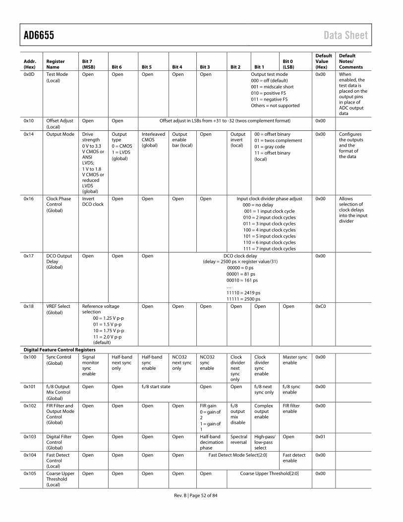
AD6655 Data Sheet
Rev. B | Page 52 of 84
Addr. (Hex)
Register Name
Bit 7 (MSB) Bit 6 Bit 5 Bit 4 Bit 3 Bit 2 Bit 1
Bit 0 (LSB)
Default Value (Hex)
Default Notes/ Comments
0x0D Test Mode (Local)
Open Open Open Open Open Output test mode 000 = off (default) 001 = midscale short 010 = positive FS 011 = negative FS Others = not supported
0x00 When enabled, the test data is placed on the output pins in place of ADC output data
0x10 Offset Adjust (Local)
Open Open Offset adjust in LSBs from +31 to -32 (twos complement format) 0x00
0x14 Output Mode Drive strength 0 V to 3.3 V CMOS or ANSI LVDS; 1 V to 1.8 V CMOS or reduced LVDS (global)
Output type 0 = CMOS 1 = LVDS (global)
Interleaved CMOS (global)
Output enable bar (local)
Open Output invert (local)
00 = offset binary 01 = twos complement 01 = gray code 11 = offset binary (local)
0x00 Configures the outputs and the format of the data
0x16 Clock Phase Control (Global)
Invert DCO clock
Open Open Open Open Input clock divider phase adjust 000 = no delay 001 = 1 input clock cycle 010 = 2 input clock cycles 011 = 3 input clock cycles 100 = 4 input clock cycles 101 = 5 input clock cycles 110 = 6 input clock cycles 111 = 7 input clock cycles
0x00 Allows selection of clock delays into the input divider
0x17 DCO Output Delay (Global)
Open Open Open DCO clock delay (delay = 2500 ps × register value/31)
00000 = 0 ps 00001 = 81 ps 00010 = 161 ps … 11110 = 2419 ps 11111 = 2500 ps
0x00
0x18 VREF Select (Global)
Reference voltage selection
00 = 1.25 V p-p 01 = 1.5 V p-p 10 = 1.75 V p-p 11 = 2.0 V p-p (default)
Open Open Open Open Open Open 0xC0
Digital Feature Control Registers
0x100 Sync Control (Global)
Signal monitor sync enable
Half-band next sync only
Half-band sync enable
NCO32 next sync only
NCO32 sync enable
Clock divider next sync only
Clock divider sync enable
Master sync enable
0x00
0x101 fS/8 Output Mix Control (Global)
Open Open fS/8 start state Open Open fS/8 next sync only
fS/8 sync enable
0x00
0x102 FIR Filter and Output Mode Control (Global)
Open Open Open Open FIR gain 0 = gain of 2 1 = gain of 1
fS/8 output mix disable
Complex output enable
FIR filter enable
0x00
0x103 Digital Filter Control (Global)
Open Open Open Open Half-band decimation phase
Spectral reversal
High-pass/ low-pass select
Open 0x01
0x104 Fast Detect Control (Local)
Open Open Open Open Fast Detect Mode Select[2:0] Fast detect enable
0x00
0x105 Coarse Upper Threshold (Local)
Open Open Open Open Open Coarse Upper Threshold[2:0] 0x00

Data Sheet AD6655
Rev. B | Page 53 of 84
Addr. (Hex)
Register Name
Bit 7 (MSB) Bit 6 Bit 5 Bit 4 Bit 3 Bit 2 Bit 1
Bit 0 (LSB)
Default Value (Hex)
Default Notes/ Comments
0x106 Fine Upper Threshold Register 0 (Local)
Fine Upper Threshold[7:0] 0x00
0x107 Fine Upper Threshold Register 1 (Local)
Open Open Open Fine Upper Threshold[12:8] 0x00
0x108 Fine Lower Threshold Register 0 (Local)
Fine Lower Threshold[7:0] 0x00
0x109 Fine Lower Threshold Register 1 (Local)
Open Open Open Fine Lower Threshold[12:8] 0x00
0x10A Increase Gain Dwell Time Register 0 (Local)
Increase Gain Dwell Time[7:0] 0x00 In ADC clock cycles
0x10B Increase Gain Dwell Time Register 1 (Local)
Increase Gain Dwell Time[15:8] 0x00 In ADC clock cycles
0x10C Signal Monitor DC Correction Control (Global)
Open DC correction freeze
DC Correction Bandwidth(k:[3:0]) DC correction for signal path enable
DC correction for signal monitor enable
0x00
0x10D Signal Monitor DC Value Channel A Register 0 (Global)
DC Value Channel A[7:0] Read only
0x10E Signal Monitor DC Value Channel A Register 1 (Global)
Open Open DC Value Channel A[13:8] Read only
0x10F Signal Monitor DC Value Channel B Register 0 (Global)
DC Value Channel B[7:0] Read only
0x110 Signal Monitor DC Value Channel B Register 1 (Global)
Open Open DC Value Channel B[13:8] Read only
0x111 Signal Monitor SPORT Control (Global)
Open RMS magnitude output enable
Peak detector output enable
Threshold crossing output enable
SPORT SMI SCLK divide
00 = Undefined 01 = divide by 2 10 = divide by 4 11 = divide by 8
SPORT SMI SCLK sleep
Signal monitor SPORT output enable
0x04
0x112 Signal Monitor Control (Global)
Complex power calculation mode enable
Open Open Open Signal monitor rms/ms select 0 = rms 1 = ms
Signal monitor mode 00 = rms/ms magnitude 01 = peak detector 10 = threshold crossing 11 = threshold crossing
Signal monitor enable
0x00
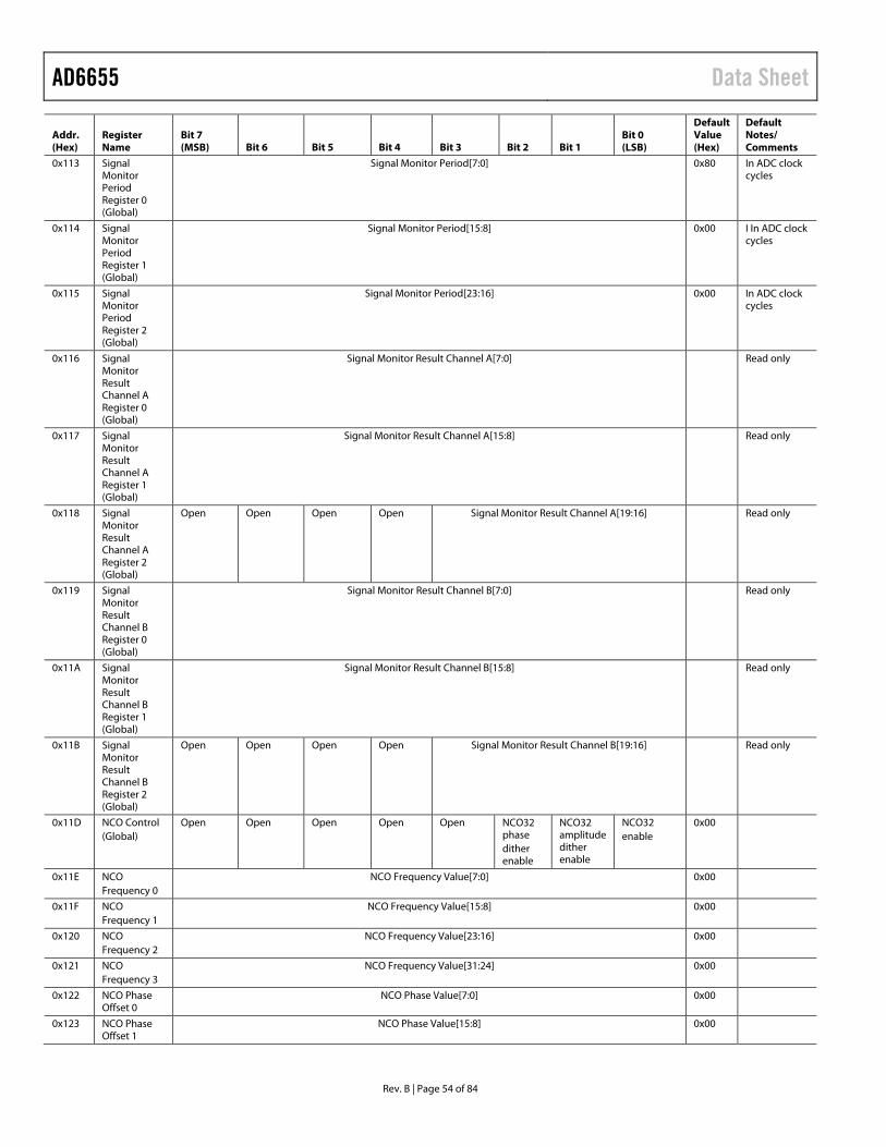
AD6655 Data Sheet
Rev. B | Page 54 of 84
Addr. (Hex)
Register Name
Bit 7 (MSB) Bit 6 Bit 5 Bit 4 Bit 3 Bit 2 Bit 1
Bit 0 (LSB)
Default Value (Hex)
Default Notes/ Comments
0x113 Signal Monitor Period Register 0 (Global)
Signal Monitor Period[7:0] 0x80 In ADC clock cycles
0x114 Signal Monitor Period Register 1 (Global)
Signal Monitor Period[15:8] 0x00 I In ADC clock cycles
0x115 Signal Monitor Period Register 2 (Global)
Signal Monitor Period[23:16] 0x00 In ADC clock cycles
0x116 Signal Monitor Result Channel A Register 0 (Global)
Signal Monitor Result Channel A[7:0] Read only
0x117 Signal Monitor Result Channel A Register 1 (Global)
Signal Monitor Result Channel A[15:8] Read only
0x118 Signal Monitor Result Channel A Register 2 (Global)
Open Open Open Open Signal Monitor Result Channel A[19:16] Read only
0x119 Signal Monitor Result Channel B Register 0 (Global)
Signal Monitor Result Channel B[7:0] Read only
0x11A Signal Monitor Result Channel B Register 1 (Global)
Signal Monitor Result Channel B[15:8] Read only
0x11B Signal Monitor Result Channel B Register 2 (Global)
Open Open Open Open Signal Monitor Result Channel B[19:16] Read only
0x11D NCO Control (Global)
Open Open Open Open Open NCO32 phase dither enable
NCO32 amplitude dither enable
NCO32 enable
0x00
0x11E NCO Frequency 0
NCO Frequency Value[7:0] 0x00
0x11F NCO Frequency 1
NCO Frequency Value[15:8] 0x00
0x120 NCO Frequency 2
NCO Frequency Value[23:16] 0x00
0x121 NCO Frequency 3
NCO Frequency Value[31:24] 0x00
0x122 NCO Phase Offset 0
NCO Phase Value[7:0] 0x00
0x123 NCO Phase Offset 1
NCO Phase Value[15:8] 0x00

Data Sheet AD6655
Rev. B | Page 55 of 84
MEMORY MAP REGISTER DESCRIPTION For more information on functions controlled in Register 0x00 to Register 0xFF, see Application Note AN-877, Interfacing to High Speed ADCs via SPI, at www.analog.com. Note that not all test modes are supported on the AD6655.
SYNC Control (Register 0x100)
Bit 7—Signal Monitor Sync Enable
Bit 7 enables the sync pulse from the external sync input to the signal monitor block. The sync signal is passed when Bit 7 and Bit 0 are high. This is continuous sync mode.
Bit 6—Half-Band Next Sync Only
If the master sync enable bit (Register 0x100, Bit 0) and the half-band sync enable bit (Register 0x100, Bit 5) are high, Bit 6 allows the NCO32 to synchronize following the first sync pulse it receives and ignore the rest. If Bit 6 is set, Bit 5 of Register 0x100 resets after this sync occurs.
Bit 5—Half-Band Sync Enable
Bit 5 gates the sync pulse to the half-band filter. When Bit 5 is set high, the sync signal causes the half-band to resynchro-nize, starting at the half-band decimation phase selected in Register 0x103, Bit 3. This sync is active only when the master sync enable bit (Register 0x100, Bit 0) is high. This is continuous sync mode.
Bit 4—NCO32 Next Sync Only
If the master sync enable bit (Register 0x100, Bit 0) and the NCO32 sync enable bit (Register 0x100, Bit 3) are high, Bit 4 allows the NCO32 to synchronize following the first sync pulse it receives and ignore the rest. Bit 3 of Register 0x100 resets after a sync occurs if Bit 4 is set.
Bit 3—NCO32 Sync Enable
Bit 3 gates the sync pulse to the 32-bit NCO. When this bit is set high, the sync signal causes the NCO to resynchronize, starting at the NCO phase offset value. This sync is active only when the master sync enable bit (Register 0x100, Bit 0) is high. This is continuous sync mode.
Bit 2—Clock Divider Next Sync Only
If the master sync enable bit (Register 0x100, Bit 0) and the clock divider sync enable bit (Register 0x100, Bit 1) are high, Bit 2 allows the clock divider to synchronize following the first sync pulse it receives and ignores the rest. Bit 1 of Register 0x100 resets after it synchronizes.
Bit 1—Clock Divider Sync Enable
Bit 1 gates the sync pulse to the clock divider. The sync signal is passed when Bit 1 and Bit 0 are high. This is continuous sync mode.
Bit 0—Master Sync Enable
Bit 0 must be high to enable any of the sync functions.
fS/8 Output Mix Control (Register 0x101)
Bits[7:6]—Reserved Bits[5:4]—fS/8 Start State
Bit 5 and Bit 4 set the starting phase of the fS/8 output mix.
Bits[3:2]—Reserved Bit 1—fS/8 Next Sync Only
If the master sync enable bit (Register 0x100, Bit 0) and the fS/8 sync enable bit (Register 0x101, Bit 0) are high, Bit 1 allows the fS/8 output mix to synchronize following the first sync pulse it receives and ignore the rest. Bit 0 of Register 0x100 resets after it synchronizes.
Bit 0—fS/8 Sync Enable
Bit 0 gates the sync pulse to the fS/8 output mix. This sync is active only when the master sync enable bit (Register 0x100, Bit 0) is high. This is continuous sync mode.
FIR Filter and Output Mode Control (Register 0x102)
Bits[7:4]—Reserved Bit 3—FIR Gain
When Bit 3 is set high, the FIR filter path, if enabled, has a gain of 1. When Bit 3 set low, the FIR filter path has a gain of 2.
Bit 2—fS/8 Output Mix Disable
Bit 2 disables the fS/8 output mix when enabled. Bit 2 should be set along with Bit 1 to enable complex output mode.
Bit 1—Complex Output Mode Enable
Setting Bit 1 high enables complex output mode.
Bit 0—FIR Filter Enable
When set high, Bit 0 enables the FIR filter. When Bit 0 is cleared, the FIR filter is bypassed and shut down for power savings.

AD6655 Data Sheet
Rev. B | Page 56 of 84
Digital Filter Control (Register 0x103)
Bits[7:4]—Reserved Bit 3—Half-Band Decimation Phase
When set high, Bit 3 uses the alternate phase of the decimating half-band filter.
Bit 2—Spectral Reversal
Bit 2 enables the spectral reversal feature of the half-band filter.
Bit 1—High-Pass/Low-Pass Select
Bit 1 enables the high-pass mode of the half-band filter when set high. Setting this bit low enables the low-pass mode (default).
Bit 0—Reserved
Bit 0 reads back as a 1.
Fast Detect Control (Register 0x104)
Bits[7:4]—Reserved Bits[3:1]—Fast Detect Mode Select
Bits[3:1] set the mode of the fast detect output bits according to Table 29.
Bit 0—Fast Detect Enable
Bit 0 is used to enable the fast detect output pins. When the FD outputs are disabled, the outputs go into a high impedance state. In LVDS mode when the outputs are interleaved, the outputs go high-Z only if both channels are turned off (power-down/ standby/output disabled). If only one channel is turned off (power-down/standby/output disabled), the fast detect outputs repeat the data of the active channel.
Coarse Upper Threshold (Register 0x105)
Bits[7:3]—Reserved Bits[2:0]—Coarse Upper Threshold
These bits set the level required to assert the coarse upper threshold indication (see Table 25).
Fine Upper Threshold (Register 0x106 and Register 0x107)
Register 0x107, Bits[7:5]—Reserved Register 0x107, Bits[4:0]—Fine Upper Threshold Bits[12:8] Register 0x106, Bits[7:0]—Fine Upper Threshold Bits[7:0]
These registers provide a fine upper limit threshold. The 13-bit value is compared to the 13-bit magnitude from the ADC block. If the ADC magnitude exceeds this threshold value, the F_UT indicator is set.
Fine Lower Threshold (Register 0x108 and Register 0x109)
Register 0x109, Bits[7:5]—Reserved Register 0x109, Bits[4:0]—Fine Lower Threshold Bits[12:8] Register 0x108, Bits[7:0]—Fine Lower Threshold Bits[7:0]
These registers provide a fine lower limit threshold. This 13-bit value is compared with the 13-bit magnitude from the ADC block. If the ADC magnitude is less than this threshold value, the F_LT indicator is set.
Increase Gain Dwell Time (Register 0x10A and Register 0x10B)
Register 0x10B, Bits[7:0]—Increase Gain Dwell Time Bits[15:8] Register 0x10A, Bits[7:0]—Increase Gain Dwell Time Bits[7:0]
These register values set the minimum time in ADC sample clock cycles (after clock divider) that a signal needs to stay below the fine lower threshold limit before the F_LT and IG are asserted high.
Signal Monitor DC Correction Control (Register 0x10C)
Bit 7—Reserved Bit 6—DC Correction Freeze
When Bit 6 is set high, the dc correction is no longer updated to the signal monitor block, which holds the last dc value calculated.
Bits[5:2]—DC Correction Bandwidth
Bits[5:2] set the averaging time of the signal monitor dc correction function. This 4-bit word sets the bandwidth of the correction block, according to the following equation:
π××= //
22__ 14k CLKf
BWCorrDC
where: k is the 4-bit value programmed in Bits[5:2] of Register 0x10C (values between 0 and 13 are valid for k; programming 14 or 15 provides the same result as programming 13). fCLK is the AD6655 ADC sample rate in hertz (Hz).
Bit 1—DC Correction for Signal Path Enable
Setting this bit high causes the output of the dc measurement block to be summed with the data in the signal path to remove the dc offset from the signal path.
Bit 0—DC Correction for Signal Monitor Enable
This bit enables the dc correction function in the signal monitor block. The dc correction is an averaging function that can be used by the signal monitor to remove dc offset in the signal. Removing this dc from the measurement allows a more accurate power reading.
Signal Monitor DC Value Channel A (Register 0x10D and Register 0x10E)
Register 0x10E, Bits[7:6]—Reserved Register 0x10E, Bits[5:0]—DC Value Channel A[13:8] Register 0x10D, Bits[7:0]—DC Value Channel A[7:0]
These read-only registers hold the latest dc offset value computed by the signal monitor for Channel A.
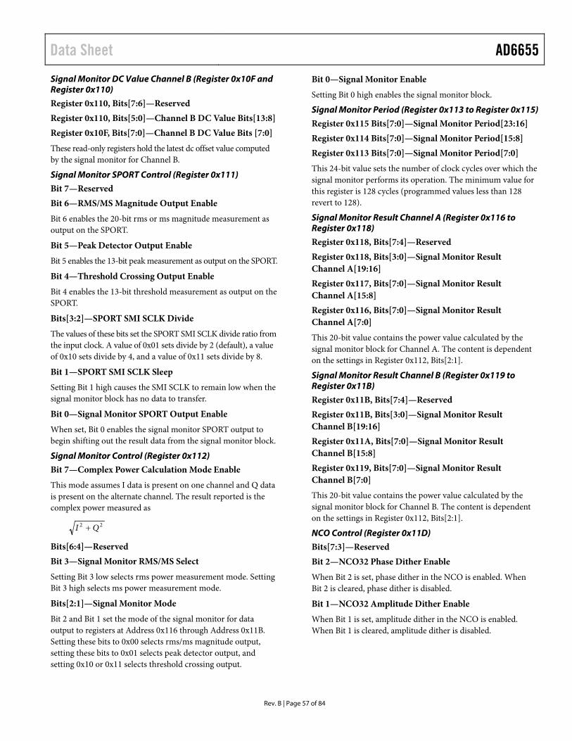
Data Sheet AD6655
Rev. B | Page 57 of 84
Signal Monitor DC Value Channel B (Register 0x10F and Register 0x110)
Register 0x110, Bits[7:6]—Reserved Register 0x110, Bits[5:0]—Channel B DC Value Bits[13:8] Register 0x10F, Bits[7:0]—Channel B DC Value Bits [7:0]
These read-only registers hold the latest dc offset value computed by the signal monitor for Channel B.
Signal Monitor SPORT Control (Register 0x111)
Bit 7—Reserved Bit 6—RMS/MS Magnitude Output Enable
Bit 6 enables the 20-bit rms or ms magnitude measurement as output on the SPORT.
Bit 5—Peak Detector Output Enable
Bit 5 enables the 13-bit peak measurement as output on the SPORT.
Bit 4—Threshold Crossing Output Enable
Bit 4 enables the 13-bit threshold measurement as output on the SPORT.
Bits[3:2]—SPORT SMI SCLK Divide
The values of these bits set the SPORT SMI SCLK divide ratio from the input clock. A value of 0x01 sets divide by 2 (default), a value of 0x10 sets divide by 4, and a value of 0x11 sets divide by 8.
Bit 1—SPORT SMI SCLK Sleep
Setting Bit 1 high causes the SMI SCLK to remain low when the signal monitor block has no data to transfer.
Bit 0—Signal Monitor SPORT Output Enable
When set, Bit 0 enables the signal monitor SPORT output to begin shifting out the result data from the signal monitor block.
Signal Monitor Control (Register 0x112)
Bit 7—Complex Power Calculation Mode Enable
This mode assumes I data is present on one channel and Q data is present on the alternate channel. The result reported is the complex power measured as
22 QI +
Bits[6:4]—Reserved Bit 3—Signal Monitor RMS/MS Select
Setting Bit 3 low selects rms power measurement mode. Setting Bit 3 high selects ms power measurement mode.
Bits[2:1]—Signal Monitor Mode
Bit 2 and Bit 1 set the mode of the signal monitor for data output to registers at Address 0x116 through Address 0x11B. Setting these bits to 0x00 selects rms/ms magnitude output, setting these bits to 0x01 selects peak detector output, and setting 0x10 or 0x11 selects threshold crossing output.
Bit 0—Signal Monitor Enable
Setting Bit 0 high enables the signal monitor block.
Signal Monitor Period (Register 0x113 to Register 0x115)
Register 0x115 Bits[7:0]—Signal Monitor Period[23:16] Register 0x114 Bits[7:0]—Signal Monitor Period[15:8] Register 0x113 Bits[7:0]—Signal Monitor Period[7:0]
This 24-bit value sets the number of clock cycles over which the signal monitor performs its operation. The minimum value for this register is 128 cycles (programmed values less than 128 revert to 128).
Signal Monitor Result Channel A (Register 0x116 to Register 0x118)
Register 0x118, Bits[7:4]—Reserved Register 0x118, Bits[3:0]—Signal Monitor Result Channel A[19:16] Register 0x117, Bits[7:0]—Signal Monitor Result Channel A[15:8] Register 0x116, Bits[7:0]—Signal Monitor Result Channel A[7:0]
This 20-bit value contains the power value calculated by the signal monitor block for Channel A. The content is dependent on the settings in Register 0x112, Bits[2:1].
Signal Monitor Result Channel B (Register 0x119 to Register 0x11B)
Register 0x11B, Bits[7:4]—Reserved Register 0x11B, Bits[3:0]—Signal Monitor Result Channel B[19:16] Register 0x11A, Bits[7:0]—Signal Monitor Result Channel B[15:8] Register 0x119, Bits[7:0]—Signal Monitor Result Channel B[7:0]
This 20-bit value contains the power value calculated by the signal monitor block for Channel B. The content is dependent on the settings in Register 0x112, Bits[2:1].
NCO Control (Register 0x11D)
Bits[7:3]—Reserved Bit 2—NCO32 Phase Dither Enable
When Bit 2 is set, phase dither in the NCO is enabled. When Bit 2 is cleared, phase dither is disabled.
Bit 1—NCO32 Amplitude Dither Enable
When Bit 1 is set, amplitude dither in the NCO is enabled. When Bit 1 is cleared, amplitude dither is disabled.
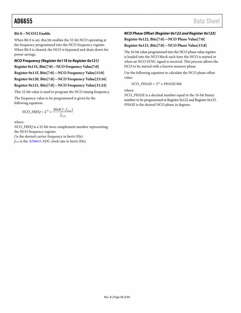
AD6655 Data Sheet
Rev. B | Page 58 of 84
Bit 0—NCO32 Enable
When Bit 0 is set, this bit enables the 32-bit NCO operating at the frequency programmed into the NCO frequency register. When Bit 0 is cleared, the NCO is bypassed and shuts down for power savings.
NCO Frequency (Register 0x11E to Register 0x121)
Register 0x11E, Bits[7:0]—NCO Frequency Value[7:0] Register 0x11F, Bits[7:0]—NCO Frequency Value[15:8] Register 0x120, Bits[7:0]—NCO Frequency Value[23:16] Register 0x121, Bits[7:0]—NCO Frequency Value[31:24]
This 32-bit value is used to program the NCO tuning frequency.
The frequency value to be programmed is given by the following equation:
CLK
CLK
fffMod
NCO_FREQ),(
232 ×=
where: NCO_FREQ is a 32-bit twos complement number representing the NCO frequency register. f is the desired carrier frequency in hertz (Hz). fCLK is the AD6655 ADC clock rate in hertz (Hz).
NCO Phase Offset (Register 0x122 and Register 0x123)
Register 0x122, Bits[7:0]—NCO Phase Value[7:0] Register 0x123, Bits[7:0]—NCO Phase Value[15:8]
The 16-bit value programmed into the NCO phase value register is loaded into the NCO block each time the NCO is started or when an NCO SYNC signal is received. This process allows the NCO to be started with a known nonzero phase.
Use the following equation to calculate the NCO phase offset value:
NCO_PHASE = 216 × PHASE/360
where: NCO_PHASE is a decimal number equal to the 16-bit binary number to be programmed at Register 0x122 and Register 0x123. PHASE is the desired NCO phase in degrees.
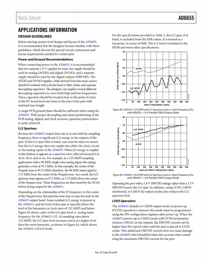
Data Sheet AD6655
Rev. B | Page 59 of 84
APPLICATIONS INFORMATION DESIGN GUIDELINES Before starting system-level design and layout of the AD6655, it is recommended that the designer become familiar with these guidelines, which discuss the special circuit connections and layout requirements needed for certain pins.
Power and Ground Recommendations
When connecting power to the AD6655, it is recommended that two separate 1.8 V supplies be used: one supply should be used for analog (AVDD) and digital (DVDD), and a separate supply should be used for the digital outputs (DRVDD). The AVDD and DVDD supplies, while derived from the same source, should be isolated with a ferrite bead or filter choke and separate decoupling capacitors. The designer can employ several different decoupling capacitors to cover both high and low frequencies. These capacitors should be located close to the point of entry at the PC board level and close to the pins of the part with minimal trace length.
A single PCB ground plane should be sufficient when using the AD6655. With proper decoupling and smart partitioning of the PCB analog, digital, and clock sections, optimum performance is easily achieved.
fS/2 Spurious
Because the AD6655 output data rate is at one-half the sampling frequency, there is significant fS/2 energy in the outputs of the part. If this fS/2 spur falls in band, care must be taken to ensure that this fS/2 energy does not couple into either the clock circuit or the analog inputs of the AD6655. When fS/2 energy is coupled in this fashion, it appears as a spurious tone reflected around fS/4, 3fS/4, 5fS/4, and so on. For example, in a 125 MSPS sampling application with a 90 MHz single-tone analog input, this energy generates a tone at 97.5 MHz. In this example, the center of the Nyquist zone is 93.75 MHz; therefore, the 90 MHz input signal is 3.75 MHz from the center of the Nyquist zone. As a result, the fS/2 spurious tone appears at 97.5 MHz, or 3.75 MHz above the center of the Nyquist zone. These frequencies are then tuned by the NCOs before being output by the AD6655.
Depending on the relationship of the IF frequency to the center of the Nyquist zone, this spurious tone may or may not exist in the AD6655 output band. Some residual fS/2 energy is present in the AD6655, and the level of this spur is typically below the level of the harmonics at clock rates of 125 MSPS and below. Figure 82 shows a plot of the fS/2 spur level vs. analog input frequency for the AD6655-125. At sampling rates above 125 MSPS, the fS/2 spur level increases and is at a higher level than the worst harmonic, as shown in Figure 83, which shows the AD6655-150 fS/2 levels.
For the specifications provided in Table 2, the fS/2 spur, if in band, is excluded from the SNR values. It is treated as a harmonic, in terms of SNR. The fS/2 level is included in the SFDR and worst other specifications.
–60
–70
–80
–90
–100
–110
–1200 50 100 150 200 250 350300 400 450 500
0670
9-08
3
INPUT FREQUENCY (MHz)
–SFDR
SFD
RA
ND
f S/2
SPU
R (d
BFS
)
fS/2 SPUR
Figure 82. AD6655-125 SFDR and fS/2 Spurious Level vs. Input Frequency (fIN)
with DRVDD = 1.8 V Parallel CMOS Output Mode
–60
–70
–80
–90
–100
–110
–1200 50 100 150 200 250 350300 400 450 500
0670
9-08
4
ANALOG INPUT FREQUENCY (MHz)
–SFDR
SFD
RA
ND
f S/2
SPU
R (d
BFS
)
fS/2 SPUR
Figure 83. AD6655-150 SFDR and fS/2 Spurious Level vs. Input Frequency (fIN)
with DRVDD = 1.8 V Parallel CMOS Output Mode
Operating the part with a 1.8 V DRVDD voltage rather than a 3.3 V DRVDD lowers the fS/2 spur. In addition, using LVDS, CMOS interleaved, or CMOS IQ output modes also reduces the fS/2 spurious level.
LVDS Operation
The AD6655 defaults to CMOS output mode on power-up. If LVDS operation is desired, this mode must be programmed using the SPI configuration registers after power-up. When the AD6655 powers up in CMOS mode with LVDS termination resistors (100 Ω) on the outputs, the DRVDD current can be higher than the typical value until the part is placed in LVDS mode. This additional DRVDD current does not cause damage to the AD6655, but it should be taken into account when consid-ering the maximum DRVDD current for the part.
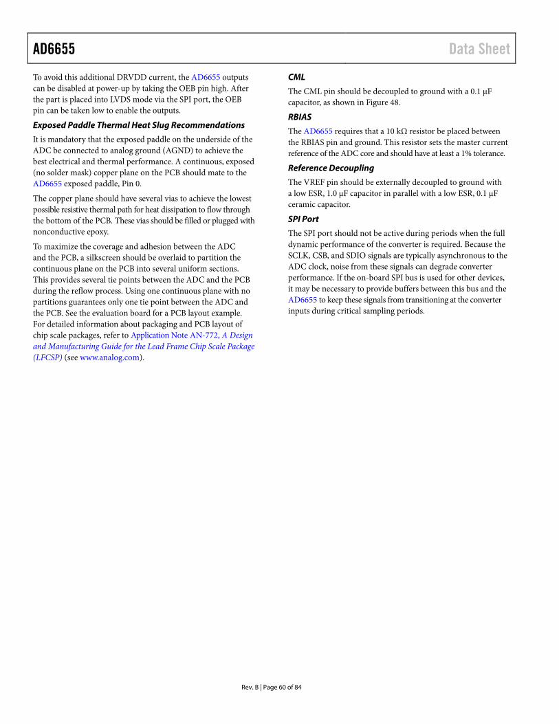
AD6655 Data Sheet
Rev. B | Page 60 of 84
To avoid this additional DRVDD current, the AD6655 outputs can be disabled at power-up by taking the OEB pin high. After the part is placed into LVDS mode via the SPI port, the OEB pin can be taken low to enable the outputs.
Exposed Paddle Thermal Heat Slug Recommendations
It is mandatory that the exposed paddle on the underside of the ADC be connected to analog ground (AGND) to achieve the best electrical and thermal performance. A continuous, exposed (no solder mask) copper plane on the PCB should mate to the AD6655 exposed paddle, Pin 0.
The copper plane should have several vias to achieve the lowest possible resistive thermal path for heat dissipation to flow through the bottom of the PCB. These vias should be filled or plugged with nonconductive epoxy.
To maximize the coverage and adhesion between the ADC and the PCB, a silkscreen should be overlaid to partition the continuous plane on the PCB into several uniform sections. This provides several tie points between the ADC and the PCB during the reflow process. Using one continuous plane with no partitions guarantees only one tie point between the ADC and the PCB. See the evaluation board for a PCB layout example. For detailed information about packaging and PCB layout of chip scale packages, refer to Application Note AN-772, A Design and Manufacturing Guide for the Lead Frame Chip Scale Package (LFCSP) (see www.analog.com).
CML
The CML pin should be decoupled to ground with a 0.1 μF capacitor, as shown in Figure 48.
RBIAS
The AD6655 requires that a 10 kΩ resistor be placed between the RBIAS pin and ground. This resistor sets the master current reference of the ADC core and should have at least a 1% tolerance.
Reference Decoupling
The VREF pin should be externally decoupled to ground with a low ESR, 1.0 μF capacitor in parallel with a low ESR, 0.1 μF ceramic capacitor.
SPI Port
The SPI port should not be active during periods when the full dynamic performance of the converter is required. Because the SCLK, CSB, and SDIO signals are typically asynchronous to the ADC clock, noise from these signals can degrade converter performance. If the on-board SPI bus is used for other devices, it may be necessary to provide buffers between this bus and the AD6655 to keep these signals from transitioning at the converter inputs during critical sampling periods.
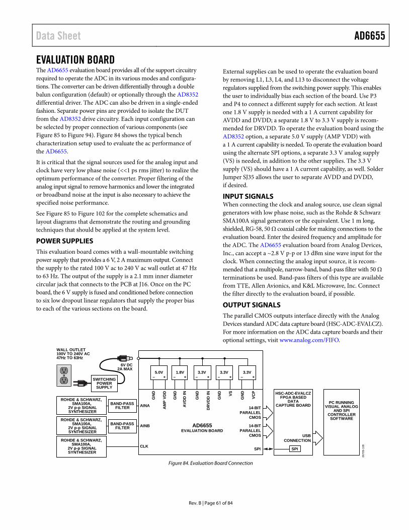
Data Sheet AD6655
Rev. B | Page 61 of 84
EVALUATION BOARD The AD6655 evaluation board provides all of the support circuitry required to operate the ADC in its various modes and configura-tions. The converter can be driven differentially through a double balun configuration (default) or optionally through the AD8352 differential driver. The ADC can also be driven in a single-ended fashion. Separate power pins are provided to isolate the DUT from the AD8352 drive circuitry. Each input configuration can be selected by proper connection of various components (see Figure 85 to Figure 94). Figure 84 shows the typical bench characterization setup used to evaluate the ac performance of the AD6655.
It is critical that the signal sources used for the analog input and clock have very low phase noise (<<1 ps rms jitter) to realize the optimum performance of the converter. Proper filtering of the analog input signal to remove harmonics and lower the integrated or broadband noise at the input is also necessary to achieve the specified noise performance.
See Figure 85 to Figure 102 for the complete schematics and layout diagrams that demonstrate the routing and grounding techniques that should be applied at the system level.
POWER SUPPLIES This evaluation board comes with a wall-mountable switching power supply that provides a 6 V, 2 A maximum output. Connect the supply to the rated 100 V ac to 240 V ac wall outlet at 47 Hz to 63 Hz. The output of the supply is a 2.1 mm inner diameter circular jack that connects to the PCB at J16. Once on the PC board, the 6 V supply is fused and conditioned before connection to six low dropout linear regulators that supply the proper bias to each of the various sections on the board.
External supplies can be used to operate the evaluation board by removing L1, L3, L4, and L13 to disconnect the voltage regulators supplied from the switching power supply. This enables the user to individually bias each section of the board. Use P3 and P4 to connect a different supply for each section. At least one 1.8 V supply is needed with a 1 A current capability for AVDD and DVDD; a separate 1.8 V to 3.3 V supply is recom-mended for DRVDD. To operate the evaluation board using the AD8352 option, a separate 5.0 V supply (AMP VDD) with a 1 A current capability is needed. To operate the evaluation board using the alternate SPI options, a separate 3.3 V analog supply (VS) is needed, in addition to the other supplies. The 3.3 V supply (VS) should have a 1 A current capability, as well. Solder Jumper SJ35 allows the user to separate AVDD and DVDD, if desired.
INPUT SIGNALS When connecting the clock and analog source, use clean signal generators with low phase noise, such as the Rohde & Schwarz SMA100A signal generators or the equivalent. Use 1 m long, shielded, RG-58, 50 Ω coaxial cable for making connections to the evaluation board. Enter the desired frequency and amplitude for the ADC. The AD6655 evaluation board from Analog Devices, Inc., can accept a ~2.8 V p-p or 13 dBm sine wave input for the clock. When connecting the analog input source, it is recom-mended that a multipole, narrow-band, band-pass filter with 50 Ω terminations be used. Band-pass filters of this type are available from TTE, Allen Avionics, and K&L Microwave, Inc. Connect the filter directly to the evaluation board, if possible.
OUTPUT SIGNALS The parallel CMOS outputs interface directly with the Analog Devices standard ADC data capture board (HSC-ADC-EVALCZ). For more information on the ADC data capture boards and their optional settings, visit www.analog.com/FIFO.
0670
9-10
8
USBCONNECTION
AD6655EVALUATION BOARD
14-BITPARALLEL
CMOS
14-BITPARALLEL
CMOS
HSC-ADC-EVALCZFPGA BASED
DATACAPTURE BOARD PC RUNNING
VISUAL ANALOGAND SPI
CONTROLLERSOFTWARE
1.8V– +– +
AVD
D IN VS
DR
VDD
IN
GN
D
GN
D
– +5.0V
GN
D
AM
P VD
D
3.3V
6V DC2A MAX
WALL OUTLET100V TO 240V AC47Hz TO 63Hz
SWITCHINGPOWERSUPPLY
– +
GN
D
3.3V
VCP
– +
GN
D
3.3V
SPI SPI
ROHDE & SCHWARZ,SMA100A,
2V p-p SIGNALSYNTHESIZER
CLK
ROHDE & SCHWARZ,SMA100A,
2V p-p SIGNALSYNTHESIZER
AINBBAND-PASSFILTER
ROHDE & SCHWARZ,SMA100A,
2V p-p SIGNALSYNTHESIZER
AINABAND-PASSFILTER
Figure 84. Evaluation Board Connection

AD6655 Data Sheet
Rev. B | Page 62 of 84
DEFAULT OPERATION AND JUMPER SELECTION SETTINGS The following is a list of the default and optional settings or modes allowed on the AD6655 evaluation board.
POWER
Connect the switching power supply that is provided in the evaluation kit between a rated 100 V ac to 240 V ac wall outlet at 47 Hz to 63 Hz and P500.
VIN
The evaluation board is set up for a double balun configuration analog input with optimum 50 Ω impedance matching from 70 MHz to 200 MHz. For more bandwidth response, the differ-ential capacitor across the analog inputs can be changed or removed (see Table 14). The common mode of the analog inputs is developed from the center tap of the transformer via the CML pin of the ADC (see the Analog Input Considerations section).
VREF
VREF is set to 1.0 V by tying the SENSE pin to ground by adding a jumper on Header J5 (Pin 1 to Pin 2). This causes the ADC to operate in 2.0 V p-p full-scale range. To place the ADC in 1.0 V p-p mode (VREF = 0.5 V), a jumper should be placed on Header J4. A separate external reference option is also included on the evalua-tion board. To use an external reference, connect J6 (Pin 1 to Pin 2) and provide an external reference at TP5. Proper use of the VREF options is detailed in the Voltage Reference section.
RBIAS RBIAS requires a 10 kΩ resistor (R503) to ground and is used to set the ADC core bias current.
CLOCK
The default clock input circuitry is derived from a simple balun-coupled circuit using a high bandwidth 1:1 impedance ratio balun (T5) that adds a very low amount of jitter to the clock path. The clock input is 50 Ω terminated and ac-coupled to handle single-ended sine wave inputs. The transformer converts the single-ended input to a differential signal that is clipped before entering the ADC clock inputs. When the AD6655 input clock divider is utilized, clock frequencies up to 625 MHz can be input into the evaluation board through Connector S5.
PDWN
To enable the power-down feature, connect J7, shorting the PDWN pin to AVDD.
CSB
The CSB pin is internally pulled up, setting the chip into external pin mode, to ignore the SDIO and SCLK information. To connect the control of the CSB pin to the SPI circuitry on the evaluation board, connect J21, Pin 1 to J21, Pin 2.
SCLK/DFS
If the SPI port is in external pin mode, the SCLK/DFS pin sets the data format of the outputs. If the pin is left floating, the pin is inter-nally pulled down, setting the default data format condition to offset binary. Connecting J2, Pin 1 to J2, Pin 2 sets the format to twos complement. If the SPI port is in serial pin mode, connecting J2, Pin 2 to J2, Pin 3 connects the SCLK pin to the on-board SPI circuitry (see the Serial Port Interface (SPI) section).
SDIO/DCS
If the SPI port is in external pin mode, the SDIO/DCS pin sets the duty cycle stabilizer. If the pin is left floating, the pin is internally pulled up, setting the default condition to DCS enabled. To disable the DCS, connect J1, Pin 1 to J1, Pin 2. If the SPI port is in serial pin mode, connecting J1, Pin 2 to J1, Pin 3 connects the SDIO pin to the on-board SPI circuitry (see the Serial Port Interface (SPI) section).
ALTERNATIVE CLOCK CONFIGURATIONS Two alternate clocking options are provided on the AD6655 evaluation board. The first option is to use an on-board crystal oscillator (Y1) to provide the clock input to the part. To enable this crystal, Resistor R8 (0 Ω) and Resistor R85 (10 kΩ) should be installed, and Resistor R82 and Resistor R30 should be removed.
A second clock option is to use a differential LVPECL clock to drive the ADC input using the AD9516 (U2). When using this drive option, the AD9516 charge pump filter components need to be populated (see Figure 89). Consult the AD9516 data sheet for more information.
To configure the clock input from S5 to drive the AD9516 reference input instead of directly driving the ADC, the following components need to be added, removed, and/or changed.
1. Remove R32, R33, R99, and R101 in the default clock path.
2. Populate C78 and C79 with 0.001 μF capacitors and R78 and R79 with 0 Ω resistors in the clock path.
In addition, unused AD9516 outputs (one LVDS and one LVPECL) are routed to optional Connector S8 through Connector S11 on the evaluation board.

Data Sheet AD6655
Rev. B | Page 63 of 84
ALTERNATIVE ANALOG INPUT DRIVE CONFIGURATION This section provides a brief description of the alternative analog input drive configuration using the AD8352. When using this particular drive option, some additional components need to be populated. For more details on the AD8352 differential driver, including how it works and its optional pin settings, consult the AD8352 data sheet.
To configure the analog input to drive the AD8352 instead of the default transformer option, the following components need to be added, removed, and/or changed for Channel A. For Channel B, the corresponding components should be changed.
1. Remove C1, C17, C18, and C117 in the default analog input path.
2. Populate C8 and C9 with 0.1 µF capacitors in the analog input path. To drive the AD8352 in the differential input mode, populate the T10 transformer; the R1, R37, R39, R126, and R127 resistors; and the C10, C11, and C125 capacitors.
3. Populate the optional amplifier output path with the desired components including an optional low-pass filter. Install 0 Ω resistors, R44 and R48. R43 and R47 should be increased (typically to 100 Ω) to increase to 200 Ω the output impedance seen by the AD8352.

AD6655 Data Sheet
Rev. B | Page 64 of 84
SCHEMATICS
06709-200
BA
IND
06031
2
123
654
IND
06031
2
912EN
B15 67
432
813
VCM
14
VIN
5
VIP16
VON
10
VOP
11
AD83
52
1
VCC
GND
GND
GND
VCC
RGN
RDN
RGP
RDP
1 2
54
123P
SF
54
123P
SF
1 1
5 4
1 2 3P
S F
IND
06031
2
1 2
IND
06031
2
DNP
DNP
DNP
OP
TIO
NA
LA
MP
LIFI
ER
INP
UT
PA
TH
DE
FAU
LTA
MP
LIFI
ER
INP
UT
PA
TH
Tran
sfor
mer
/am
pch
anne
lA
AIN
+
AIN
-
DNP
DNP
DNP
L16
180N
H
R31
0O
HM
C16
0.00
1U
R5
57.6OHM
R1
57.6OHM
R28
57.6OHM
R126
4.12K
R27
33O
HM
R26
33O
HM
R41
10KOHM
R40
10K
OH
M
S2
AMP+
A
L17
180N
H
VIN
-A
AVDD
R50
0O
HM
VIN
+A
AMP+
A
AMP-
A
INA+INA-
INA
-
INA+
ETC
1-1-
13
T10
C12
5.3
PF
R127
100OHM
R12
1
RES
0402 0
OH
M
R4
0OHM
R48
0O
HM
R49
0O
HM
R47
33OHM
R43
33OHM
R42
0O
HM
R44
0O
HM
R11
0
0O
HM
R2
0O
HM
R12
0
0O
HM
R39
0O
HM
R38
DN
P
R37
0O
HM
R36
DNP
R54
0O
HM
R35
24.9OHM
R29
24.9OHM
TP15
TP14
C27
10U
C23
0.1U
C22
0.1U
ETC
1-1-
13
T2
ETC
1-1-
13
T1
CML
CML
AVDD
AMP-
A
AMPV
DD
C9 0.1U
C4 18PF
C13
912
PF
C5 4.7P
F
C12
0.00
1U
C3 0.1U
C1 0.1U
C8 0.1U
C10
0.1U C
11
0.1U
C47
0.1U
C11
7
0.1U
C17
0.1U
C18
0.1U
C2 0.1U
S1
Z1
L14
120N
H
AD
T1_1
WT
T7
L15
120N
H
AMPV
DD
W1
AMPV
DD
Figure 85. Evaluation Board Schematic, Channel A Analog Inputs
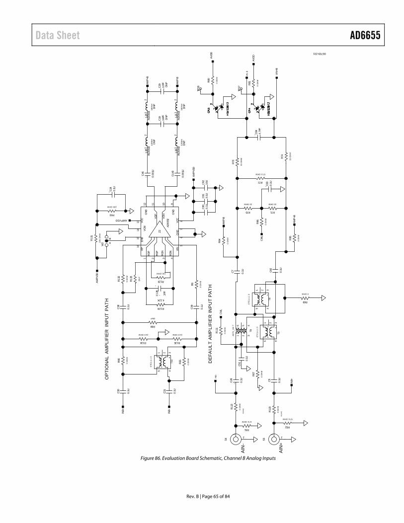
Data Sheet AD6655
Rev. B | Page 65 of 84
06709-201
BA
ENB
VCM
VIN
VIP
VON
VOP
AD83
52
VCC
GND
GND
GND
VCC
RGN
RDN
RGP
RDP
PS F
IND
0603
IND
0603
IND
0603
IND
0603
PS F
PS F
DNP
DNP
DNP
DNP
DNP
OP
TIO
NA
LA
MP
LIFI
ER
INP
UT
PA
TH
DE
FAU
LTA
MP
LIFI
ER
INP
UT
PA
TH
AIN
+
AIN
-
DNP
R13
3
DNP
R72
57.6OHM
R52
57.6OHM
R51
57.6OHM
R128
4.12K
R73
33O
HM R
74
33O
HM
R70
33OHM
R71
33OHM
R53
10KOHM
AMPV
DD
R13
1
10K
OH
M
R135
24.9OHM
R129
100OHM
R69
0OHM
R67
0O
HM
R12
3
RES
04020
OH
MR12
2
RES
04020
OH
M
R11
1
0O
HM
R94
0O
HM R95
0O
HM
R96
0O
HM
R81
0O
HMR80
0O
HM
R55
0O
HM
R6
0O
HM
R68
DNP
R134
24.9OHM
R13
2
0O
HM
R66
0O
HM
321
45
ETC
1-1-
13
T4
456
321ADT1
_1W
T
T8
321
45
ETC
1-1-
13
T3
C51
0.1U
C28
0.1U
INB
-
INB+
CM
LAM
P-B
AMP+
B
CM
L
VIN
-B
AVDDAV
DD
AMP-
B
AMP+
B
AMPVDD
INB-
INB+
C19
18PF
C29
12PF
C84
4.7P
F
C12
8
.3PF
C46
0.00
1U
C14
0
0.00
1U
C38
0.1U
C30
0.1U
C31
0.1U
C82
0.1U
C83
0.1U
C24
0.1U
C7 0.1U
C39
0.1U
C6 0.1U
21
S3
21
S4
1TP16
1TP17
12
L19
120N
H
12
L21
180N
H
12
L20
180N
H
12
L18
120N
H
321
45
ETC
1-1-
13
T11
912
67
15
41 32
813
51614
1011
Z2
W2
C62
10U
C61
0.1U
C60
0.1U
AMPV
DD
VIN
+B
Figure 86. Evaluation Board Schematic, Channel B Analog Inputs

AD6655 Data Sheet
Rev. B | Page 66 of 84
06709-202
PS F
ENC
ENC
\
VS
C14
5
0.1U
C20
0.1U
R85
10KOHM
R8
0OHM
21
TP2
R84
24.9
OHM
R79
0O
HM
R34
DNP
R10
1
0O
HM
R3
0O
HM
R7
57.6OHM
R90
0O
HM
R30
57.6OHM
R32
0O
HM
R33
0O
HM
R99
0O
HM
R78
0O
HM
R82
10KOHM
ALTC
LK-
C64
0.00
1U
C94
0.00
1U
321
45
ETC
1-1-
13T5
C79
0.00
1U
OPT
_CLK
-
CLK
-
CLK
+
OPT
_CLK
+
OPT
_CLK
+
C77
0.00
1U
C78
0.00
1U
C63
0.00
1U
C56
0.1U
C21
0.1U
21
SMA2
00U
PS6
21
SMA2
00U
PS5
4 5 6
3 2 1 AD
T1_1
WT
T9
OPT
_CLK
-
ALTC
LK+
R83
24.9OHM
Figure 87. Evaluation Board Schematic, DUT Clock Input

Data Sheet AD6655
Rev. B | Page 67 of 84
06709-203
TEST
TEST
TEST
BYPA
SS_L
D O
CL K
C P
CP_RSET
GN
D_E
SD
GN
D_O
UT8
9_D
I V
GND_REF
LD LF NC1
NC2
NC3
NC4
OUT0
OUT1
OU
T2
OU
T3
OUT4
OUT5
OU
T6
OU
T7
OU
T8
OU
T 9
REFIN
REF
MON
REF
_SEL
RSET_CLOCKSC
LK
SDIO
SDO
STAT
US
VCP
VS_C
LK_D
IST
VS_OUT01_DI V
VS_OUT01_DRV
VS_O
UT2
3_D
IV
VS_O
UT2
3_D
RV
VS_OUT45_DI V
VS_OUT45_DRV
VS_OUT67_1
VS_OUT67_2 VS_OUT89_1
VS_OUT89_2
VS_P
LL_1
VS_PLL_2
VS_PRESCALER
VS_REF
VS_V
CO
CLK
B
CSB
OUT0B
OUT1B
OU
T2B
OU
T3B
OUT4B
OUT5B
OU
T6B
OU
T7B
OU
T8B
OU
T9B
PDB
REFINB
RESETB
SYN
CBAD
9516
_64L
FCS P
PAD
2
AD95
16C
LKIN
LVD
SO
UTP
UT
LVPE
CL
OU
TPU
T
TOAD
CLV
PEC
L
1
S 7
VCXO
_CLK
-
R89
49.9OHM
R12
4.12K
R9
100OHM
R75
100OHM
1TP8
2
1
S11
OU
T6P
OU
T6N
10 1 35
62
44 37
59
3 9 15
18
19
20
56
53
43 40
25
28
48 46 3335
2 7
58
22
21
64 12
51
54
3841
30
27
49
50 31
32
61
60
57
11 14
17
55
52
42 39
26
29
47 45 3436
24
63
23
81 16
64
U2
200
R91
200
R86
R11
5.1K
200
R88
200
R92
R12
5
RES
040 20
OH
M
R12
4
RES
040 20
OH
M
R10
0O
HM
C10
40.
1U
C10
10.
1 UC
9 80.
1 UC
9 90.
1 UC
9 60.
1 UC
970.
1 U
C10
00.
1 U
SYNC
VCP
VS
_OU
T_D
R
VCXO
_CLK
+
1
TP1 8
L D1
TP1 9 C80
18P F
C14
1
0.00
1 U
C8 6
0.1U
C8 5
0.1 U
C8 7
0.1 U
C8 8
0.1U
C14
3
0.1 U
C14
2
0.1U
2
1
S10
2
1
S92
1
S8
1TP
20
OP
T_C
LK+
SCLKV S
SYN
C B
RESETB
OP
T_C
LK-
PDB
CSB_2
VS
VS
VS
VS
VS
VS_OUT_DR
VS_O
UT_
DR
VS
VS_O
UT_
D R
VCP
SDO
SDI
REF
_SEL LF
AGND
AGN DAG
NDCP
BYPA
SS_L
D O
STAT
U S
REF
MO N
ALTC
LK-
ALTC
LK+
Figure 88. Evaluation Board Schematic, Optional AD9516 Clock Circuit

AD6655 Data Sheet
Rev. B | Page 68 of 84
06709-204
A1 GND
A2
Y1
VCC Y2
OU
T2
OU
T1
VCC
GND
OU
T_D
ISAB
LE
FREQ
_CTR
L_V VS
-500
VAL
VAL
VAL
VAL
VAL
Cha
rge
Pum
pFi
lter
SYNC
VS
VS
C14
4SE
L
C92
SEL
C89
SEL
R93
R87
24.9OHM
R98
R13
6R
137
R97
R11
7
RES
04020
OH
M
R11
6
RES
04020
OH
M
R108
RES0402
10KOHM
R109
RES0402
10KOHM
R107
RES0402
10KOHM
R106
RES0402
10KOHM
R13
9
RES
04020
OH
M
R11
4
RES
04020
OH
M
R105
RES0402
10KOHM
R103
RES0402
10KOHM
R102
RES0402
10KOHM
R100
RES0402
10KOHM
SYNC
R10
4
RES
04020
OH
M
R46
RES
040233
OH
M
200
R76
R45
RES0603
57.6OHM
LD
RES
ETB
SYN
CB
PDB
REF
_SE
L
VSVS
VSVS VC
XO_C
LK-
VCXO
_CLK
+
VCP
VCP
LF
CP
456
321 U25
OSC
VEC
TRO
N_V
S500
C91
SEL
C90
SEL
C25
0.1U
C26
0.1U
21
SMA2
00U
PS1
2
1TP1
456
321
NL2
7WZ0
4
U3
BYPA
SS_L
DO
Figure 89. Evaluation Board Schematic, Optional AD9516 Loop Filter/VCO and SYNC Input

Data Sheet AD6655
Rev. B | Page 69 of 84
06709-205
J7-I
NS
TALL
FOR
PD
WN
J8-I
NS
TALL
FOR
OU
TPU
TDIS
AB
LE
J5- I
NS
TALL
FOR
IVV
RE
F/2V
INP
UTS
PAN
J4- I
NS
TALL
FOR
0.5V
VR
EF/
IVIN
PU
TS
PAN
J6-I
NS
TALL
FOR
EX
TER
NA
LRE
FER
EN
CE M
ODE
1234567891011121 314151 6
4 847464 5444342414039383 736353433
49
50
51
52
53
54
55
56
57
58
59
60
61
62
63
64
32
31
30
29
28
27
26
25
24
23
22
21
20
19
18
17
U1
AVDD
R112
RES0402
0OHM
R11
5 RES
0402
0O
H M
R11
3 RES
0402
0O
HM
1TP
6
R6 3
RES
0402
10K O
HM
C15
1U
9 10 11 12 13 1 4 15 16
8 7 6 5 4 3 2 1
22oh
m
RPA
K8
R60
9 10 11 1 2 1 3 1 4 15 16
8 7 6 5 4 3 2 1
22oh
mR
PAK8
R59
FD0 B
9 10 11 1 2 1 3 1 4 15 16
8 7 6 5 4 3 2 1
22oh
m
RPA
K 8
R5 7
FD1B
FD2 B
FD3B
D0 B
D1B
D2 B
D3B
D4B
D5B
D13
BD
12B
D11
BD
10B
D9B
D8B
D7 B
D6 B
DC
OBD
COA
D0 A
D1A
D2A
D3A
D4 A
D5A
D6A
D7A
D8A
D9A
D10
AD
11A
D12
AD
13A
DVD
D
AVD
D
PWR_SDFS
FD0A
PWR_SDOPWR_SCLK
FD3AFD2AFD1A
DR
VDD
C10
90.
1UC
121
0.1U
C12
20.
001 U
C12
60.
001U
C12
70.
001U
C34
0.1U
C33
0.00
1U
C35
0.00
1UC36
0.1 U
C3 2
0.1U
C14
0.1U
C4 0
0.1 U
C12
00.
1U5 6 7 8
4 3 2 1
22oh
mR
PAK4
R5 8
9 1 0 11 12 13 14 15 16
8 7 6 5 4 3 2 1
22oh
m
RPA
K8
R6 1
1TP
3
1 TP5
910111213141516
87654321
22ohmRPAK8
R62
DVDD DVDD
SYNC
SPI_CSB
CLK-
CLK+
AVDD
VIN
+A
VIN
- A
VIN
-B
VIN
+B
AVD
D
AVD
D
SPI_
SDIO
SPI_
SCLK
DR
VDD
CML
DR
VDD
C13
70.
001U
R64
RES
0402
0O
HM
AVD
D1
AVD
D2
CLK+
CLK-
CM
L
D0B_LSB_
D10A
D10
B
D11A
D11
B
D12A
D12
B
D13A_MSB_
D13
B_M
SB_
D1A
D1B
D2A
D2B
D3A
D3B
D4A
D4B
D5A
D5BD6A
D6B
D7A
D7B
D8A
D8B
D9A
D9B
DC
OA
DC
OB
DO
A_LS
B_
DRGND
DRGND1
DR
VDD
DRVDD1
DVDD1DVDD2
FD0AFD0B
FD1A
FD1B
FD2A
FD2B
FD3A
FD3B
AVD
D3
PWR
_SC
LK_P
DW
N
PWR
_SD
FS
PWR
_SD
O/O
EB
RBI
AS
SEN
SE
SPI_CSB
SPI_
SCLK
/DFS
SPI_
SDIO
/DC
S
SYNCVI
N+A
VIN
+B
VIN
-A
VIN
- B
VREF
AD66
5 5
Figure 90. Evaluation Board Schematic, DUT

AD6655 Data Sheet
Rev. B | Page 70 of 84
06709-206
TEST
TEST
TEST
TEST
VAL
CH
AN
NE
LA
CH
AN
NE
LB
DIG
ITAL
/HSC
-AD
C-E
VALC
ZIN
TER
FAC
E
484746454443424140393837363534333231302928272625
123456789101112131415161718192021222324
74VC
X162
244M
TD
U17
484746454443424140393837363534333231302928272625
123456789101112131415161718192021222324
74VC
X162
244M
TD
U16
484746454443424140393837363534333231302928272625
123456789101112131415161718192021222324
74VC
X162
244M
TD
U15
SDI
CSB
SCLK
R14
5
RES
04020
OHM
R14
2
RES
04020
OHM
SDO
R14
1
RES
04020
OHM
R11
9
RES
04020
OHM
CSB
_2
V_D
IG
VS R140
RES0402
10KOHM
R118
RES0402
10KOHM
R130 R77
100OHM
SYN
C
OU
T6N
OU
T6P
OU
T6P
OU
T6N
FD0B
FD1B
DG
10D
G9
DG
8D
G7
DG
6D
G5
DG
4D
G3
DG
2D
G1
A1A2A3A 4A5A6A7A8A9 A10
B1 B2B3B4B5B6B7B8B9 B10
C1
C2
C3
C4
C5
C6
C7
C8
C9
C10 D1
D2
D3
D4
D5
D6
D7
D8
D9
D10
BG10
BG9
BG8
BG7
BG6
BG5
BG4
BG3
BG2
BG1
TYCO
_HM
-ZD
J11
V_D
IG
V_D
IG
FD2B
FD3B
D0B
D1B
D2B
D3B
V_D
IGD
4BD
5B
D6B
D7B
V_D
IGV_D
IGV_
DIG
V_D
IG
D8B
D9B
D10
BD
11B
D12
BD
13B
DC
OBD
COA
D0A
D1A
D2A
D3A
D4A
D5A
D6A
D7A
D8A
D9A
D10
AD
11A
V_D
IGD
12A
D13
A
FD3A
FD2A
FD1A
FD0A
V_D
IG
PW
R_S
DO
PWR
_SD
FSSC
LK_O
UT
SDFS
_OU
T
SD
O_O
UT
PWR
_SC
LK
SD
O_O
UT
1TP
23SCLK
_OUT
SD
FS_O
UT
1
TP21
V_D
IG
C65
0.1U
VS
C71
0.1U
C70
0.1U
C69
0.1U
C68
0.1U
C66
0.1U
C67
0.1U
C72
0.1U
C73
0.1U
C76
0.1U
C74
0.1U
C75
0.1U
RES
ETB
DG
10D
G9
DG
8D
G7
DG
6D
G5
DG
4D
G3
DG
2D
G1
A1 A2 A3 A4 A5 A6 A7 A8 A9A10
B1B2 B3 B4 B5 B6 B7 B8 B9B10
C1
C2
C3
C4
C5
C6
C7
C8
C9
C10D
1
D2
D3
D4
D5
D6
D7
D8
D9
D10
BG10
BG9
BG8
BG7
BG6
BG5
BG4
BG3
BG2
BG1
TYC
O_H
M-Z
D
J12
DG
10D
G9
DG
8D
G7
DG
6D
G5
DG
4D
G3
DG
2D
G1
A1A2A3A4A5A6A7A8A9 A10
B1 B2B3B4B5B6B7B8B9 B10
C1
C2
C3
C4
C5
C6
C7
C8
C9
C10 D1
D2
D3
D4
D5
D6
D7
D8
D9
D10
BG10
BG9
BG8
BG7
BG6
BG5
BG4
BG3
BG2
BG1
TYCO
_HM
-ZD
J10
1
TP22
1TP
24
V_D
IG
R14
3
RES
04020
OHM
R14
4
RES
04020
OHM
Figure 91. Evaluation Board Schematic, Digital Output Interface

Data Sheet AD6655
Rev. B | Page 71 of 84
06709-207
Y1
VCC Y2
A1 GN
D
A2
Y1
VCC Y2
A1 GN
D
A2
J1-J
UM
PE
RP
INS
2TO
3FO
RS
PIO
PE
RA
TION
JUM
PE
RPI
NS
1TO
2FO
RD
CS
EN
AB
LEJ2
-JU
MP
ER
PIN
S2
TO3
FOR
SP
IOP
ER
ATI
ONJU
MP
ER
PIN
S1
TO2
FOR
TWOS
CO
MP
LIME
NTO
UTP
UT
J21
-IN
STA
LLJU
MP
ER
FOR
SP
IOP
ER
ATI
ON
13
J2
13
J1
CSB
_2
R23
RES
0603
100K
OHM
R22
RES
0603
100K
OHM
R17
RES
0603
100K
OHM
R65
RES0402
10KOHM
C81
0.1U
R24
RES
040210KO
HM
R21
RES
06031K
OHM
R19
RES
06031K
OHM
R18
RES
040210KO
HM
R20
RES
06031K
OHM
C13
0.1U
SDI
SDO
SCLK
CSB
V_D
IG
SDI
VS
SDO
V_D
IG
V_D
IG
V_D
IG
SPI_
SDIO SP
I_SC
LK
SPI_
CSB
V_D
IG
V_D
IG
V_D
IG
SCLK
CSB
321
456
NC
7WZ1
6P6X
U8
321
456
NC
7WZ0
7P6X
U7
Figure 92. Evaluation Board Schematic, SPI Circuitry

AD6655 Data Sheet
Rev. B | Page 72 of 84
06709-208
1P1
2P2
3P3
4P4
5P5
6P6
P1 P2 P3 P4
SMD
C11
0F
GND
INPA
D4
OUT
AD
P33
34
3FB
GND 5
8IN IN
27
1O
UTO
UT2
2
SD 6
BIAS
PSG
CB CG CG
CG
6V,
2AM
AX
POW
ERIN
PUT
BNX-
016
OPT
ION
ALPO
WER
SUPP
LYIN
PUT
S
DR
VDD
SETT
ING
DR
VDD
R1
3R
14
3.3
1.8
2.5
140
K
107
K
76.8
K
78.7
K
94.0
K
147
K
GN
DTE
STPO
INT
S
1 3
2 4 5 6
F1
VR1
21
S2A
_RE
CT
CR
12
21
S2A
_RE
CT
CR
112
1SHO
T_R
ECT
CR8
2 1
S2A_REC T
CR7
1
3AD
P333
9
VR3
VS
DR
VD
DI
N
C10
30.
1U
SJ35
AV
DD
IN
C10
210
U
C52
10U
VCP
F2P
WR
_IN
21
S2A
_RE
CT
CR
10
C42
1U
231
POW
ER_J
ACK
J16
C53
10U
C54
10U
C41
10U
C59
0.1U
C58
0.1U
C57
0.1U
1TP4
21
10u
hIN
D12
10
L3
1TP25
V_D
IG
DVD
D
DR
VD
D
AV
DD
DR
VD
DI
N
AV
DD
IN C45
1UC
441U
C43
1U
C93
0.00
1U
P4
12
L6IN
D12
10
10U
H
1TP13
1TP12
1TP10
1TP9
21
10u
h
IND
1210
L11
21
10u
h
IND
1210
L10
21
10u
h
IND
1210 L4
21
10U
HIN
D12
10
L9
P3
R16
RES0603
261OHM
R13
76.8KOHM
R14
147KOHM
Figure 93. Evaluation Board Schematic, Power Supply
Data Sheet AD6655
Rev. B | Page 73 of 84
06709-209
AD
P33
34
FBG
ND
IN IN2
OU
TO
UT2
SD
GND
INPA
D4
OU
T
GND
INPA
D4
OU
T
GND
INPA
D4
OU
T
Pow
erS
uppl
yB
y Pas
sC
apac
i tor s
1
3AD
P333
9
VR6
1
3AD
P333
9
VR5
1
3AD
P333
9
VR4
SJ36
SJ37
C12
410
UC
118
10U
C11
910
U
C10
80.
1UC
105
0.1U
C11
60.
1 UC
107
0.1 U
C11
30.
1 U
VS
C11
40.
1UC
115
0.1U
C11
10.
1UC
112
0.1 U
C11
00.
1U
21
10u h
IND
121 0
L12
AMPV
DD
C12
91U
VCP
VCP
VSVS_O
UT_
DR
3
5
8 71 2
6
VR
2
C13
51U
C13
61U
C13
21U
C13
11U
C13
41 U
C13
31U
C13
01U
C95
0.00
1U
21
10uh
IND
1210
L13
21
10UH
IND
1210 L1
21
10UH
IND
1210 L8
PW
R_I
N
PW
R_I
N
PW
R_I
N
PW
R_I
N
R15
78.7KOHM
R25
140KOHM
VCP
VS
_OU
T_DR
VS
Figure 94. Evaluation Board Schematic, Power Supply (Continued)

AD6655 Data Sheet
Rev. B | Page 74 of 84
EVALUATION BOARD LAYOUTS
0670
9-10
0
Figure 95. Evaluation Board Layout, Primary Side

Data Sheet AD6655
Rev. B | Page 75 of 84
0670
9-10
1
Figure 96. Evaluation Board Layout, Ground Plane
AD6655 Data Sheet
Rev. B | Page 76 of 84
0670
9-10
2
Figure 97. Evaluation Board Layout, Power Plane
Data Sheet AD6655
Rev. B | Page 77 of 84
0670
9-10
3
Figure 98. Evaluation Board Layout, Power Plane
AD6655 Data Sheet
Rev. B | Page 78 of 84
0670
9-10
4
Figure 99. Evaluation Board Layout, Ground Plane

Data Sheet AD6655
Rev. B | Page 79 of 84
0670
9-10
5
Figure 100. Evaluation Board Layout, Secondary Side (Mirrored Image)

AD6655 Data Sheet
Rev. B | Page 80 of 84
0670
9-10
6
Figure 101. Evaluation Board Layout, Silkscreen, Primary Side

Data Sheet AD6655
Rev. B | Page 81 of 84
0670
9-10
7
Figure 102. Evaluation Board Layout, Silkscreen, Secondary Side

AD6655 Data Sheet
Rev. B | Page 82 of 84
BILL OF MATERIALS
Table 30. Evaluation Board Bill of Materials (BOM)1, 2
Item Qty Reference Designator Description Package Manufacturer Mfg. Part Number
1 1 AD6655CE_REVB PCB PCB Analog Devices
2 55 C1 to C3, C6, C7, C13, C14, C17, C18, C20 to C26, C32, C57 to C61, C65 to C76, C81 to C83, C96 to C101, C103, C105, C107, C108, C110 to C116, C145
0.1 µF, 16 V ceramic capacitor, SMT 0402
C0402SM Murata GRM155R71C104KA88D
3 1 C80 18 pF, COG, 50 V, 5% ceramic capacitor, SMT 0402
C0402SM Murata GJM1555C1H180JB01J
4 2 C5, C84 4.7 pF, COG, 50 V, 5% ceramic capacitor, SMT 0402
C0402SM Murata GJM1555C1H4R7CB01J
5 10 C33, C35, C63, C93 to C95, C122, C126, C127, C137
0.001 µF, X7R, 25 V, 10% ceramic capacitor, SMT 0402
C0402SM Murata GRM155R71H102KA01D
6 13 C15, C42 to C45, C129 to C136
1 µF, X5R, 25 V, 10% ceramic capacitor, SMT 0805
C0805 Murata GR4M219R61A105KC01D
7 10 C27, C41, C52 to C54, C62, C102, C118, C119, C124
10 µF, X5R, 10 V, 10% ceramic capacitor, SMT 1206
C1206 Murata GRM31CR61C106KC31L
8 1 CR5 Schottky diode HSMS2822, SOT23 SOT23 Avago Technologies HSMS-2822-BLKG
9 2 CR6, CR9 LED RED, SMT, 0603, SS-type LED0603 Panasonic LNJ208R8ARA
10 4 CR7, CR10 to CR12 50 V, 2 A diode DO_214AA Micro Commercial Components S2A-TP
11 1 CR8 30 V, 3 A diode DO_214AB Micro Commercial Components SK33-TP
12 1 F1 EMI filter FLTHMURATABNX01 Murata BNX016-01
13 1 F2 6.0 V, 3.0 A, trip current resettable fuse
L1206 Tyco Raychem NANOSMDC150F-2
14 2 J1, J2 3-pin, male, single row, straight header
HDR3 Samtec TWS-1003-08-G-S
15 9 J4 to J9, J18, J19, J21
2-pin, male, straight header HDR2 Samtec TWS-102-08-G-S
16 3 J10 to J12 Interface connector TYCO_HM_ZD Tyco 6469169-1
17 1 J14 8-pin, male, double row, straight header
CNBERG2X4H350LD Samtec TSW-104-08-T-D
18 1 J16 DC power jack connector PWR_JACK1 Cui Stack PJ-002A
19 10 L1, L3, L4, L6, L8 to L13
10 µH, 2 A bead core, 1210 1210 Panasonic EXC-CL3225U1
20 1 P3 6-terminal connector PTMICRO6 Weiland Electric, Inc. Z5.531.3625.0
21 1 P4 4-terminal connector PTMICRO4 Weiland Electric, Inc. Z5.531.3425.0
22 3 R7, R30, R45 57.6 Ω, 0603, 1/10 W, 1% resistor
R0603 NIC Components NRC06F57R6TRF
23 27 R2, R3, R4, R32, R33, R42, R64, R67, R69, R90, R96, R99, R101, R104, R110 to F113, R115, R119, R121, R123, R141 to R145
0 Ω, 1/16 W, 5% resistor R0402SM NIC Components NRC04ZOTRF
24 1 R13 76.8 kΩ, 0603, 1/10 W, 1% resistor R0603 NIC Components NRC06F7682TRF
25 1 R25 140 kΩ, 0603, 1/10 W, 1% resistor R0603 NIC Components NRC06F1403TRF
26 1 R14 147 kΩ, 0603, 1/10 W, 1% resistor R0603 NIC Components NRC06F1473TRF
27 1 R15 78.7 kΩ, 0603, 1/10 W, 1% resistor R0603 NIC Components NRC06F7872TRF

Data Sheet AD6655
Rev. B | Page 83 of 84
Item Qty Reference Designator Description Package Manufacturer Mfg. Part Number
28 1 R16 261 Ω, 0603, 1/10 W, 1% resistor R0603 NIC Components NRC06F2610TRF
29 3 R17, R22, R23 100 kΩ, 0603, 1/10 W, 1% resistor R0603 NIC Components NRC06F1003TRF
30 7 R18, R24, R63, R65, R82, R118, R140
10 kΩ, 0402, 1/16 W, 1% resistor R0402SM NIC Components NRC04F1002TRF
31 3 R19, R21 1 kΩ, 0603, 1/10 W, 1% resistor R0603 NIC Components NRC06F1001TRF
32 9 R26, R27, R43, R46, R47, R70, R71, R73, R74
33 Ω, 0402, 1/16 W, 5% resistor R0402SM NIC Components NRC04J330TRF
33 5 R57, R59 to R62 22 Ω, 16-pin, 8-resistor, resistor array
R_742 CTS Corporation 742C163220JPTR
34 1 R58 22 Ω, 8-pin, 4-resistor, resistor array
RES_ARRY CTS Corporation 742C083220JPTR
35 1 R76 200 Ω, 0402, 1/16 W, 1% resistor R0402SM NIC Components NCR04F2000TRF
36 4 S2, S3, S5, S12 SMA, inline, male, coaxial connector
SMA_EDGE Emerson Network Power
142-0701-201
37 1 SJ35 0 Ω, 1/8 W, 1% resistor SLDR_PAD2MUYLAR NIC Components NRC10ZOTRF
38 5 T1 to T5 Balun TRAN6B M/A-COM MABA-007159-000000
39 1 U1 IC, AD6655 LFCSP64-9X9-9E Analog Devices AD6655BCPZ
40 1 U2 Clock distribution, PLL IC LFCSP64-9X9 Analog Devices AD9516-4BCPZ
41 1 U3 Dual inverter IC SC70_6 Fairchild Semiconductor NC7WZ04P6X_NL
42 1 U7 Dual buffer IC, open-drain circuits
SC70_6 Fairchild Semiconductor NC7WZ07P6X_NL
43 1 U8 UHS dual buffer IC SC70_6 Fairchild Semiconductor NC7WZ16P6X_NL
44 3 U15 to U17 16-bit CMOS buffer IC TSOP48_8_1MM Fairchild Semiconductor 74VCX16244MTDX_NL
45 2 VR1, VR2 Adjustable regulator LFCSP8-3X3 Analog Devices ADP3334ACPZ
46 1 VR3 1.8 V high accuracy regulator SOT223-HS Analog Devices ADP3339AKCZ-1.8
47 1 VR4 5.0 V high accuracy regulator SOT223-HS Analog Devices ADP3339AKCZ-5.0
48 2 VR5, VR6 3.3 V high accuracy regulator SOT223-HS Analog Devices ADP3339AKCZ-3.3
49 1 Y1 Oscillator clock, VFAC3 OSC-CTS-CB3 Valpey Fisher VFAC3-BHL
50 2 Z1, Z2 High speed IC, op amp LFCSP16-3X3-PAD Analog Devices AD8352ACPZ
1 This bill of materials is RoHS compliant. 2 The bill of materials lists only those items that are normally installed in the default condition. Items that are not installed are not included in the BOM.
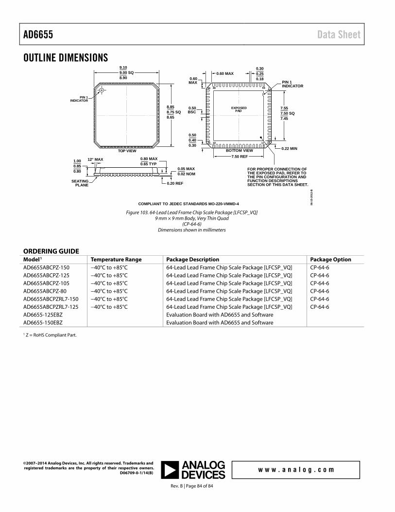
AD6655 Data Sheet
Rev. B | Page 84 of 84
OUTLINE DIMENSIONS
COMPLIANT TO JEDEC STANDARDS MO-220-VMMD-4
0.22 MIN
164
1617
4948
3233
0.500.400.30
0.50BSC
0.20 REF
12° MAX 0.80 MAX0.65 TYP
1.000.850.80
7.50 REF
0.05 MAX0.02 NOM
0.60 MAX0.60MAX
SEATINGPLANE
PIN 1INDICATOR
7.557.50 SQ7.45
PIN 1INDICATOR
0.300.250.18
FOR PROPER CONNECTION OFTHE EXPOSED PAD, REFER TOTHE PIN CONFIGURATION ANDFUNCTION DESCRIPTIONSSECTION OF THIS DATA SHEET.
TOP VIEW
EXPOSEDPAD
BOTTOM VIEW
9.109.00 SQ8.90
8.858.75 SQ8.65
06-1
5-20
12-B
Figure 103. 64-Lead Lead Frame Chip Scale Package [LFCSP_VQ]
9 mm × 9 mm Body, Very Thin Quad (CP-64-6)
Dimensions shown in millimeters
ORDERING GUIDE Model1 Temperature Range Package Description Package Option AD6655ABCPZ-150 −40°C to +85°C 64-Lead Lead Frame Chip Scale Package [LFCSP_VQ] CP-64-6 AD6655ABCPZ-125 −40°C to +85°C 64-Lead Lead Frame Chip Scale Package [LFCSP_VQ] CP-64-6 AD6655ABCPZ-105 −40°C to +85°C 64-Lead Lead Frame Chip Scale Package [LFCSP_VQ] CP-64-6 AD6655ABCPZ-80 −40°C to +85°C 64-Lead Lead Frame Chip Scale Package [LFCSP_VQ] CP-64-6 AD6655ABCPZRL7-150 −40°C to +85°C 64-Lead Lead Frame Chip Scale Package [LFCSP_VQ] CP-64-6 AD6655ABCPZRL7-125 −40°C to +85°C 64-Lead Lead Frame Chip Scale Package [LFCSP_VQ] CP-64-6 AD6655-125EBZ Evaluation Board with AD6655 and Software AD6655-150EBZ Evaluation Board with AD6655 and Software 1 Z = RoHS Compliant Part.
©2007–2014 Analog Devices, Inc. All rights reserved. Trademarks and registered trademarks are the property of their respective owners. D06709-0-1/14(B)