ieee xplore full-text pdf
TRANSCRIPT

IEEE JOURNAL OF SOLID-STATE CIRCUITS, VOL. 48, NO. 5, MAY 2013 1151
A 90-nm CMOS 5-GHz Ring-Oscillator PLLWith Delay-Discriminator-Based Active
Phase-Noise CancellationSeungkee Min, Member, IEEE, Tino Copani, Associate Member, IEEE, Sayfe Kiaei, Fellow, IEEE, and
Bertan Bakkaloglu, Senior Member, IEEE
Abstract—Ring oscillators (ROs) provide a low-cost digital VCOsolution in fully integrated PLLs. However, due to their supplynoise sensitivity and high noise floor, their applications have beenlimited to low-performance applications. The proposed archi-tecture introduces an analog feed-forward adaptive phase-noisecancellation architecture that extracts and suppresses phase noiseof ROs outside the PLL bandwidth. The proposed technique canimprove the phase noise at an arbitrary offset frequency andbandwidth, and, after initial calibration for gain, it is insensitiveto process, voltage, and temperature variations. An experimentalfractional PLL, with a loop bandwidth of 200 kHz, is utilized todemonstrate the active phase-noise cancellation approach. Thecancellation loop is designed to suppress the phase noise at 1-MHzoffset by 12.5 dB and reference spur by 13 dB with less than 17%increase in the overall power consumption at 5.1-GHz frequency.The measured phase noise at 1-MHz offset after cancellation is105 dBc/Hz. The proposed RO-PLL is fabricated in 90-nm
CMOS process. With noise cancellation loop enabled, the PLLconsumes 24.7 mA at 1.2-V supply.
Index Terms—Delay-discriminator, frequency synthesizer,phase-locked loop (PLL), ring-oscillator VCO.
I. INTRODUCTION
V OLTAGE-CONTROLLED oscillators (VCOs) are oneof the most critical blocks in phase-locked loops (PLLs).
LC-tank VCOs have a superior phase-noise performance.However, they require bulky passive resonators and calibra-tion to overcome their limited tuning range. Ring-oscillator(RO)-based VCOs are attractive for digital system applica-tions owing to their ease of integration, small die area, andscalability in deep submicron processes. However, due to theirsupply sensitivity and poor phase-noise performance, theyhave limited use in applications demanding low phase-noisefloor, such as wireless or optical transceivers. Particularly, theout-of-band phase noise of RO-based PLLs is dominated by
Manuscript received September 10, 2012; revised January 17, 2013; acceptedJanuary 18, 2013. Date of publication March 29, 2013; date of current versionApril 19, 2013. This paper was approved by Guest Editor Srenik Mehta.S. Min was with Arizona State University, Tempe, AZ 85287 USA. He is now
with the RF Division, Freescale Semiconductor, Tempe, AZ 85259 USA.T. Copani was with Arizona State University, Tempe, AZ 85287 USA. He is
nowwith theMixed Process Division, IBPGroup, STMicroelectronics, Catania,95121 Italy (e-mail: [email protected]).S. Kiaei and B. Bakkaloglu are with Arizona State University, Tempe, AZ
85287 USA.Color versions of one or more of the figures in this paper are available online
at http://ieeexplore.ieee.org.Digital Object Identifier 10.1109/JSSC.2013.2252515
the RO noise floor, which cannot be suppressed by the loopgain. Wide-loop-bandwidth PLLs can suppress RO phase noiseat higher frequencies; however, they suffer from increasedin-band noise due to contributions generated by reference,phase detectors, and charge-pumps. Most phase-noise cancella-tion schemes reported so far have been targeting deterministic
modulator quantization noise in fractional- synthesizers[3]. These approaches enable wider loop bandwidths andcancel close-in phase noise due to quantization error in thefractional controller. However, they cannot track and cancelrandom phase errors in a PLL. Recently, different approacheshave been proposed to minimize PLL phase noise outside loopbandwidth through cancellation [2]–[5]. A current-steeringDAC in parallel with the charge-pump is employed in [3] tocancel the modulator quantization noise in a fractional- PLL.In [4], a dedicated supply regulator is used to attenuate the ROsupply noise at the cost of reduced supply voltage headroomand power efficiency. An auxiliary circuit with inverse delaysensitivity to supply noise is used to compensate for the delayvariation of inverter cells in [5].In this paper, an online feed-forward phase-noise extraction
and cancellation technique based on a delayed-discriminatorphase detector is presented. The proposed circuit can attenuatethe RO phase noise in an arbitrary band of interest. This ap-proach can cancel both the ambient and inherent device noisewithout the need for online calibration. The cancellation pathgain and bandwidth tracks process, voltage, and temperaturevariations (PVT). Due to gain and bandwidth tracking, aone-time calibration is sufficient. The implemented noise-can-celling loop can enable RO-PLL-based frequency synthesizersto be utilized in high-sensitivity applications requiring lowphase noise, such as broadband tuners and RF transceivers.The remainder of this paper is organized as follows. Section II
introduces the proposed PLL architecture. Section III shows thetransistor-level implementations. Measurement results are pre-sented in Section IV. Finally, Section V draws the conclusions.
II. PROPOSED ARCHITECTURE
A. Time Domain Noise Cancellation Analysis
As shown in Fig. 1(a), in a free-running RO, each variabledelay cell exhibits random phase error due to device, supply andsubstrate noise. When the RO VCO is locked within a PLL, thephase error accumulation is filtered by the PLL dynamics. Asshown in Fig. 1(b), the dc and low-frequency components of theVCO control voltage determine the close-in phase noise. Within
0018-9200/$31.00 © 2013 IEEE

1152 IEEE JOURNAL OF SOLID-STATE CIRCUITS, VOL. 48, NO. 5, MAY 2013
Fig. 1. Phase noise and jitter accumulation in (a) a free-running RO, (b) a phase-locked RO, and (c) in the proposed delay-discriminator-based noise cancellationarchitecture.
the PLL loop bandwidth, deviations of the VCO frequency islocked to the reference clock and is attenuated by the PLL loopgain. The phase noise of the VCO outside the PLL bandwidthis dominated by the RO’s noise floor characteristic and our ap-proach tries to address noise performance in this region.There are several techniques to measure the phase noise and
jitter of integrated oscillators. In [1], a delay line and mixer (i.e.,delay-line discriminator) was used to convert the instantaneousphase deviations of an oscillator to voltage deviations, enablingan on-chip real-time phase noise measurement. This techniquedoes not require a spectrally clean reference clock and can ex-tract the phase noise for a wide range of frequency offsets fromthe carrier frequency. As shown in Fig. 2, the proposed PLLutilizes a similar delay-line discriminator to measure the RO’sinstantaneous phase noise in a selected bandwidth and to cancelthe phase noise with a voltage-controlled delay element outsidethe PLL. The delay element is matched with the VCO delaysand tracks the PVT variations of the VCO.As shown in Fig. 1(c), the existing delay elements inside the
RO can also be used for the delay-line discriminator delay line.The two inputs of the discriminator mixer shown in Fig. 1(c)are represented by and its delayed version . Thesignals and can be represented by
(1)
where is the RO signal swing with oscillation frequency. The spot phase noise can be represented by the peak sinu-
soidal jitter level at a frequency offset , and is the ROline delay. Assuming signal swing of the VCO for simplicityunity , the output of the mixer is representedas follows:
(2)
As shown in (2), the mixer output contains the sum and differ-ence of the delay chain signal phase terms. After filtering higherharmonics, the mixer output can be represented by
(3)
where is the discriminator gain in V/rad. Assuming aquadrature phase shift between the two mixer inputs, where

MIN et al.: 90-nm CMOS 5-GHZ RO PLL WITH DELAY-DISCRIMINATOR-BASED ACTIVE PHASE-NOISE CANCELLATION 1153
Fig. 2. Block diagram of the delay-discriminator-based feed-forward phase-noise cancellation PLL.
, and small phase-noise modulation index (0.2 rad), the bandpass filter (BPF) output is represented by
(4)
Assuming a small-signal deviation, the small-signal transferfunction for the discriminator becomes [1]
(5)
As shown in (5), the discriminator measures the RO phasenoise at a given frequency offset, amplified by the RO delayand discriminator gain . It is important to note that a smallquadrature error only impacts the gain of the discriminator path.Assuming an imperfect quadrature generation,, here represents the quadrature error, and the cancellationsignal becomes
(6)
Using small-signal approximation, the cancellation signalbecomes
(7)
Assuming a static quadrature phase error , the cancellationsignal only incurs a gain error, which can be calibrated at thefactory. As shown in Fig. 2, a BPF is required to suppress thecancellation path flicker noise. The high-pass filter before thecancellation delay element allows the PLL to control the dcand low-frequency VCO frequency shifts, which is important toset the steady state output frequency and reduce in-band phasenoise. Therefore, in the proposed approach, the PLL controls thesteady-state VCO frequency, while the cancellation path sup-presses the far-out phase noise. In order to achieve effectivephase-noise cancellation, the differential BPF output is invertedand applied to the auxiliary delay stage outside the PLL. In gen-eral, the VCO output phase without cancellation can be repre-sented in the time domain by
(8)
The output of the cancellation delay cell becomes
(9)
where is the auxiliary delay cell sensitivity in rad/V. Asdiscussed in Section IV, the gain of the delay discriminator pathis designed to match the delay characteristics of the main VCO.As shown in (9), the VCO output phase noise within the BPFbandwidth is cancelled by the delay cell outside the VCO.
B. Frequency-Domain Noise Cancellation Analysis
Fig. 3 shows a phase-domain linearized ac model of the activenoise cancellation VCO within a PLL. In this model the feed-forward path is represented by the mixer gain block , BPFtransfer function and the auxiliary delay element delay
. The input-referred noise of the VCO is represented by, and the PLL output phase noise after cancellation
can be represented by
(10)
1154 IEEE JOURNAL OF SOLID-STATE CIRCUITS, VOL. 48, NO. 5, MAY 2013
Fig. 3. PLL small-signal model for active noise cancellation.
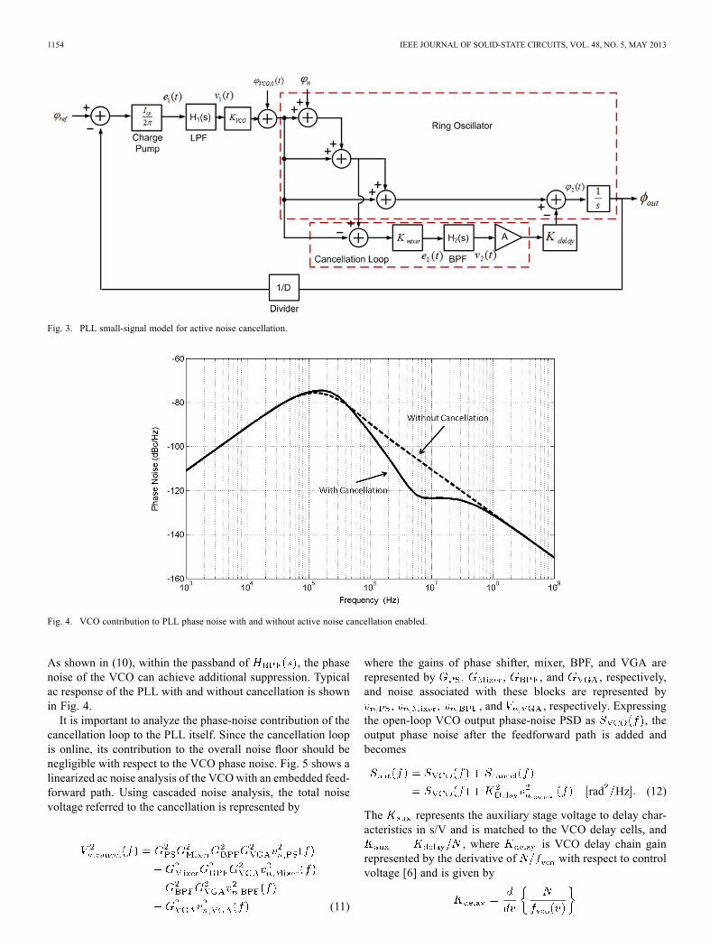
Fig. 4. VCO contribution to PLL phase noise with and without active noise cancellation enabled.
As shown in (10), within the passband of , the phasenoise of the VCO can achieve additional suppression. Typicalac response of the PLL with and without cancellation is shownin Fig. 4.It is important to analyze the phase-noise contribution of the
cancellation loop to the PLL itself. Since the cancellation loopis online, its contribution to the overall noise floor should benegligible with respect to the VCO phase noise. Fig. 5 shows alinearized ac noise analysis of the VCOwith an embedded feed-forward path. Using cascaded noise analysis, the total noisevoltage referred to the cancellation is represented by
(11)
where the gains of phase shifter, mixer, BPF, and VGA arerepresented by , and , respectively,and noise associated with these blocks are represented by
, and , respectively. Expressingthe open-loop VCO output phase-noise PSD as , theoutput phase noise after the feedforward path is added andbecomes
rad Hz (12)
The represents the auxiliary stage voltage to delay char-acteristics in s/V and is matched to the VCO delay cells, and
, where is VCO delay chain gainrepresented by the derivative of with respect to controlvoltage [6] and is given by

MIN et al.: 90-nm CMOS 5-GHZ RO PLL WITH DELAY-DISCRIMINATOR-BASED ACTIVE PHASE-NOISE CANCELLATION 1155
Fig. 5. Linearized ac noise model of cancellation loop.
Fig. 6. Noise contribution of the feed-forward path in comparison to an open-loop, uncancelled VCO and individual noise contributions of the cancellationloop.
when
(13)
It is important to note that, for an stage VCO, the VCO gainis given by
(14)
where is VCO frequency in PLL when it is locked, andrepresents the voltage to delay gain of the auxiliary delay
cell used in cancellation.As shown in (14), the VCO frequency gain is times
greater than the individual delay cell voltage characteristics,which reduces the noise contributions of the feed-forward pathby . As shown in Fig. 6, the noise contribution of thefeed-forward path to an open-loop, uncancelled VCO at 1-MHzoffset is around 20 dB lower than the VCO itself. The feed-for-ward noise contribution is 12 dB lower than the cancelled VCO,ensuring no significant noise impact on the overall VCO floornoise.
III. NOISE CANCELLATION CIRCUIT IMPLEMENTATION
Fig. 7 shows the block diagram of the proposed PLL withRO and adaptive feed-forward phase-noise-cancelling circuit.The noise-cancelling loop consists of an active polyphase filterfor quadrature generation, discriminator mixer, BPF, and a vari-able gain amplifier (VGA) for gain calibration. The cancella-
tion is independent of voltage and temperature variations, whichminimizes any further calibration. One-time calibration is per-formed to ensure that the feed-forward phase noise measure-ment chain gain to match the VCO gain. The gain is calibratedby sweeping VGA gain settings until a minimum phase noiseat 1-MHz offset is achieved. After the calibration, the feed-for-ward path gain and VCO gain track each other across PVT, asdescribed in Section III-B. It is important to note that the calibra-tion is performed only on the gain and cancellation bandwidth ofthe path, and these settings are performed only on the BPF andthe VGA driving the final correction gain stage. The schematicof the proposed RO and delay-discriminator-based noise-can-celling loop is shown in Fig. 8.
A. Active Inductor Ring Oscillator
The RO is implemented with five pseudo-differential variabledelay inverter cells shown in Fig. 8. The delay cell topology usesactive inductors to compensate for the parasitic capacitances [7]and increase the delay cell speed. Active inductors have severaladvantages over passive inductors, including substantial reduc-tion in die area and minimum substrate noise coupling in com-parison to passive inductors. However, they have significantlyhigher active device noise in comparison to passive inductors.The noise-cancelling architecture is a very good candidate forthis topology, since it suppresses the noise generated due to theactive inductor devices in the band of interest. The active induc-tors are realized by MOS active loads Mn -Mn and variableresistors Mg -Mg . The inductance value is determined by theequivalent resistance at Mn -Mn gate.By adjusting the triode resistance , the effective
impedance at the inverter is controlled as follows:
(15)
The stage delay time constant is represented byas
(16)
From (16), inductance of the active inductor is directlytuned by varying resistance . Furthermore, active in-ductor load of delay cell is significantly smaller than passiveinductor load. The measured tuning curve of the oscillator isshown in Fig. 14.
B. Feed-Forward Active Noise Cancellation Path
As shown in the discriminator analysis, quadrature phaseshift between the two mixer inputs, where ,achieves maximum phase discriminator sensitivity and lin-earity at the mixer output. An active -C polyphase filter isused in the discriminator input to maintain quadrature opera-tion at the mixer input. The implementation of the polyphasefilter with constant Gm biasing is shown in Fig. 10. Following

1156 IEEE JOURNAL OF SOLID-STATE CIRCUITS, VOL. 48, NO. 5, MAY 2013
Fig. 7. Schematics of RO delay cells with active inductors and feed-forward noise-cancelling loop.
Fig. 8. RO delay cell with active inductors.
Fig. 9. Schematic of constant Gm biasing for PPF, TIA, and VGA.
the polyphase filter, fully differential double-balanced pas-sive mixer with transimpedance amplifier (TIA) provides afirst-order low-pass filtering and frequency discrimination. Apassive mixer operating in triode mode is selected to achieve
Fig. 10. Active polyphase filter with constant Gm biasing.
high phase discrimination linearity and low flicker noise. TheRC pole in the TIA feedback path determines the cancellationbandwidth and helps with rejection of higher harmonics at themixer output. Fig. 11 shows the TIA used in the mixer. Thecombined gain of the active polyphase filter followed by thepassive mixer is represented by as follows:
(17)
where is the polyphase filter transconductance, andis the passive mixer transimpedance gain. As shown in Fig. 9,the filter is kept constant by the beta-multiplier basedbiasing circuit, and the degeneration resistance is matched with
. This ensures a process and temperature independent gain

MIN et al.: 90-nm CMOS 5-GHZ RO PLL WITH DELAY-DISCRIMINATOR-BASED ACTIVE PHASE-NOISE CANCELLATION 1157
Fig. 11. Schematic of TIA stage amplifier used in the BPF and mixer.
Fig. 12. Digitally controlled symmetric load VGA for phase-noise extractiongain calibration and its interface to cancellation delay cell.
Fig. 13. Die micrograph of the active noise-cancellation PLL.
for . The gain variation across 80 C is reduced from2 dB down to 0.4 dB. The low-frequency component of the dis-criminator output is proportional to the steady-state frequencyof the RO. Since the RO steady state frequency is determinedby the PLL, the low frequency components of the cancella-tion path need to be filtered before it is applied to the VCO.As shown in Fig. 7, a DC feedback path through andremoves DC components at the mixer output providing a highpass pole [8]. High-pass cut-off frequency of the proposed filter
Fig. 14. Frequency range with respect to control voltage across temperatureand process.
is controlled by the of the feedback OTA and low-passcut-off is controlled by 1/RC of the feed-forward TIA feedbacknetwork. To extend the bandwidth of the phase noise extrac-tion path, either the transresistance gain needs to be reduced,which increases noise and increases the TIA power, or the TIAfeedback capacitor should be reduced, which also increases thepower consumption of the TIA to achieve dominant pole sta-bility. The high-pass cut-off frequency of the BPF is controlledby changing transconductance and . In the proposedsystem, the HPF pole is placed around 20 kHz, and the low-passpole of the BPF is at 20 MHz. A fully differential VGA pro-vides a gain tuning for process variations in the variable-delaycell tuning characteristics.This gain adjustment is done once in a factory setting and
can be fixed for the regular operation. The gain matching ofthe feed-forward path is performed by sweeping VGA gain set-tings until a minimum phase noise at the BPF center frequencyis achieved. The digitally controlled VGA that is used for this
1158 IEEE JOURNAL OF SOLID-STATE CIRCUITS, VOL. 48, NO. 5, MAY 2013
Fig. 15. Feed-forward cancellation path gain variation with and without con-stant bias.
Fig. 16. Measured PLL output phase noise with and without phase-noise can-cellation at frequencies of (a) 4.9 GHz and (b) 5.2 GHz.
calibration and its interface to the delay cell is shown in Fig. 12.The VGA performs differential to single-ended conversion ofthe control signal, and adding the static offset bias from a replicabias of the RO. After initial gain calibration, the feed-forward
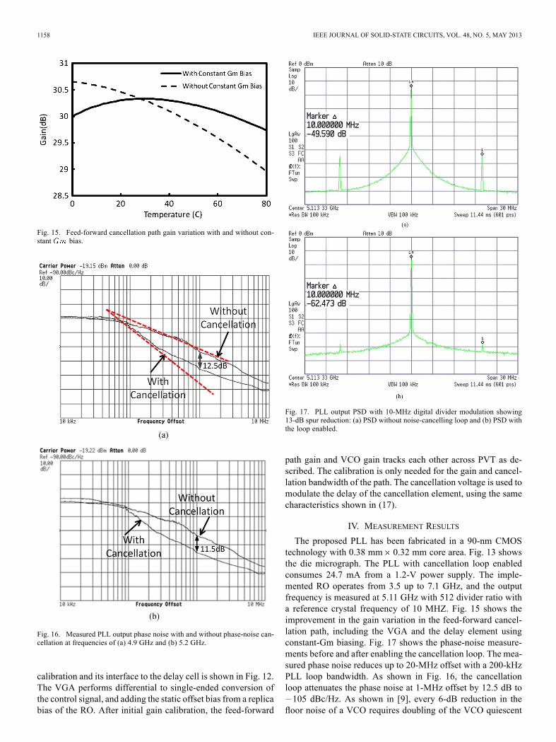
Fig. 17. PLL output PSD with 10-MHz digital divider modulation showing13-dB spur reduction: (a) PSD without noise-cancelling loop and (b) PSD withthe loop enabled.
path gain and VCO gain tracks each other across PVT as de-scribed. The calibration is only needed for the gain and cancel-lation bandwidth of the path. The cancellation voltage is used tomodulate the delay of the cancellation element, using the samecharacteristics shown in (17).
IV. MEASUREMENT RESULTS
The proposed PLL has been fabricated in a 90-nm CMOStechnology with 0.38 mm 0.32 mm core area. Fig. 13 showsthe die micrograph. The PLL with cancellation loop enabledconsumes 24.7 mA from a 1.2-V power supply. The imple-mented RO operates from 3.5 up to 7.1 GHz, and the outputfrequency is measured at 5.11 GHz with 512 divider ratio witha reference crystal frequency of 10 MHZ. Fig. 15 shows theimprovement in the gain variation in the feed-forward cancel-lation path, including the VGA and the delay element usingconstant-Gm biasing. Fig. 17 shows the phase-noise measure-ments before and after enabling the cancellation loop. The mea-sured phase noise reduces up to 20-MHz offset with a 200-kHzPLL loop bandwidth. As shown in Fig. 16, the cancellationloop attenuates the phase noise at 1-MHz offset by 12.5 dB to105 dBc/Hz. As shown in [9], every 6-dB reduction in the
floor noise of a VCO requires doubling of the VCO quiescent

MIN et al.: 90-nm CMOS 5-GHZ RO PLL WITH DELAY-DISCRIMINATOR-BASED ACTIVE PHASE-NOISE CANCELLATION 1159
Fig. 18. Performance comparison of state-of-the-art ring oscillators with re-spect to the proposed approach, with and without active noise cancellation.
TABLE IPLL PERFORMANCE SUMMARY
current. Following this model, a 12-dB reduction in the VCOphase noise would require increase in the VCO power. Theproposed approach achieves this reduction with only 35% in-crease in the VCO power and 17% increase in the overall PLLpower to achieve this reduction. On the other hand, the adopted90-nm CMOS node, the die area of the core VCO is increasedby 50% due to the cancellation path. The die area overhead ismainly due to the tunable BPF. Fig. 18 shows the performanceof the proposed approach with and without the feed-forwardpath enabled. The proposed approach can also be used in frac-tional- applications. Fig. 17 shows PLL output PSD beforeand after the cancellation when the feedback divider is modu-lated to achieve a fractional division. The cancellation
loop reduces the 10-MHz reference spur tone by 13 dB. This re-sult shows that the proposed architecture can also be used tomit-igate out-of-band quantization noise of fractional- frequencysynthesizers. The performance of the implemented PLL is sum-marized in the Table I.
V. CONCLUSION
An RO-based PLLwith active noise cancellation is integratedin 90-nm CMOS process. The active noise-cancellation circuitmeasures and cancels the phase noise in a selected bandwidthby using a similar delay element as used in the main VCO. Thefeed-forward cancellation circuit tracks the process and tem-perature variations of the VCO delay element, requiring onlya one-time gain adjustment. The proposed approach can sup-press several ambient noise sources also, such as supply andsubstrate noise. A 12-dB phase noise reduction is achieved withonly 35% increase in the VCO power and 17% increase in theoverall PLL power. The measured phase noise at 1 MHz offsetafter enabling the feed-forward path is 105 dBc/Hz. The cir-cuit performs over 12.5 dB of phase noise reduction at 10-MHzoffset and 13 dB of reference spur rejection.
REFERENCES
[1] W. Khalil, B. Bakkaloglu, and S. Kiaei, “A self-calibrated on-chipphase-noise-measurement circuit with 75 dBc single-tone sensitivityat 100 kHz offset,” in ISSCC Dig. Tech. Papers, 2007, pp. 546–547.
[2] A. Elshazly, R. Inti, W. Yin, B. Young, and P. K. Hanumolu, “0.4-to-3GHz digital PLL with supply-noise cancellation using deterministicbackground calibration,” in ISSCCDig. Tech. Papers, 2011, pp. 92–94.
[3] H. Hedayati, B. Bakkaloglu, and W. Khalil, “A 1 MHz bandwidthtype-i fractional-N synthesizer for WiMAX applications,” inISSCC Dig. Tech. Papers, 2009, pp. 390–391.
[4] E. Alon, J. Kim, S. Pamarti, K. Chang, andM.Horowitz, “Replica com-pensated linear regulators for supply-regulated phase-locked loops,”IEEE J. Solid-State Circuits, vol. 41, no. 2, pp. 413–424, Feb. 2006.
[5] M. Mansuri and C.-K. K. Yang, “A low-power low-jitter adaptive-bandwidth PLL and clock buffer,” in ISSCC Dig. Tech. Papers, 2003,pp. 430–440.
[6] S. Ye, L. Jansson, and I. Galton, “A multiple-crystal interface PLL withVCO realignment to reduce phase noise,” IEEE J. Solid-State Circuits,vol. 37, no. 12, pp. 1795–1803, Dec. 2002.
[7] S. Hara, T. Tokumitsu, T. Tanaka, and M. Aikawa, “Broadband mono-lithic microwave active inductor and its application to miniaturizedwideband amplifier,” IEEE Trans. Microw. Theory Tech., vol. 36, no.12, pp. 1920–1924, Dec. 1988.
[8] R. Harjani, J. Kim, and J. Harvey, “DC-coupled IF stage design for a900-MHz ISM receiver,” IEEE J. Solid-State Circuits, vol. 38, no. 1,pp. 126–134, Jan. 2003.
[9] T. C.Weigandt, “Low-phase-noise, low-timing-jitter design techniquesfor delay cell based VCOs and frequency synthesizers,” Ph.D. disserta-tion, Dept. Electr. Eng. Comput. Sci., Univ. California, Berkeley, CA,USA, 1998.
[10] K. H. Cheng, Y. C. Tsai, Y. L. Lo, and J. S. Huang, “0.5-V0.4–2.24-GHz inductorless phase-locked loop in a system-on-chip,”IEEE Trans. Circuits Syst. I, Reg. Papers, vol. 58, no. 5, pp. 849–859,May 2011.
[11] Z.-Z. Chen and T.-C. Lee, “The design and analysis of dual-delay-pathring oscillators,” IEEE Trans. Circuits Syst. I, Reg. Papers, vol. 58, no.3, pp. 470–478, Mar. 2011.
[12] L. H. Qi, G. W. Ling, S. Liter, L. W. Meng, and Z. Y. Ping, “A low-noise multi-GHz CMOS multi-loop ring oscillator with coarse and finefrequency tuning,” IEEE Trans. Very Large-Scale Integr. (VLSI) Syst.,vol. 17, no. 4, pp. 571–577, Apr. 2009.
[13] H. Q. Liu, W. L. Goh, and L. Siek, “A 0.18- m 10-GHz CMOS ringoscillator for optical transceivers,” in Proc. IEEE Int. Symp. CircuitsSyst., May 2005, vol. 2, pp. 1525–1528.

1160 IEEE JOURNAL OF SOLID-STATE CIRCUITS, VOL. 48, NO. 5, MAY 2013
SeungkeeMin (M’12) received the B.S. degree fromIllinois Institute of Technology, Chicago, IL, USA, in2004, and the M.S. degree from Pennsylvania StateUniversity, State College, PA, USA, in 2007, and thePh.D. degree from Arizona State University, Tempe,AZ in 2011, all in electrical engineering.He is currently an RF Design Engineer with
Freescale Semiconductor, Tempe, AZ, USA. Hiscurrent research interests including RF and analogintegrated circuits.
Tino Copani (A’08) was born in Catania, Italy, in1972. He received the Laurea degree in electronicsengineering and Ph.D. degree in electronics and au-tomation engineering from the University of Catania,Catania, Italy, in 1998 and 2004, respectively.From 2000 to 2004, he was with the Radio
Frequency Advanced Design Group, a joint re-search group between the University of Catania andSTMicroelectronics, where he was involved withthe design and development of RFICs for satellitecommunications. In 2005, as a Post-Doctoral Re-
search Associate, he joined Connection One Center, Arizona State University,Tempe, AZ, USA. Since December 2010, he has been with the Mixed ProcessDivision, STMicroelectronics, Catania, Italy, where he is involved in thedesign of BiCMOS RFICs for wireless infrastructures. His current researchinterest is the design of VCOs, frequency synthesizers, and building blocks forlow-power RFICs and MMICs.
Sayfe Kiaei (F’12) received the Ph.D. degree fromthe University of Washington, Seattle, WA, USA, in1987.He was a Senior Member of Technical Staff with
the Wireless Technology Center and BroadbandOperations at Motorola from 1993–2001 where hewas responsible for the development of WirelessTransceiver IC’s, and Digital Subscriber Lines(DSL) transceivers. Before joining Motorola, he wasan Associate Professor with Oregon State Universityfrom 1987 to 1993, where he taught courses and
performed research in digital communications, VLSI system design, advancedCMOS IC design, and wireless systems. He is currently a Professor and theDirector of the Connection One Center (NSF I/UCRC Center) at Arizona StateUniversity, Tempe, AZ, USA, where he is also currently the Associate Deanof Research.Dr. Kiaei is a member of the IEEE Circuits and Systems Society, the IEEE
Solid State Circuits Society, and the IEEE Communication Society. He hasbeen on the technical program committee and/or chair of many conferences, in-cluding: RFIC, MTT, ISCAS, and other international conferences. He has pub-lished over 100 journal and conference papers and holds several patents and hisresearch interests are in wireless transceiver design, RF and Mixed-Signal IC’sin CMOS and SiGe. He was the recipient of the Carter Best Teacher Award ofthe Oregon State College of Engineering, the IEEE Darlington Award, and theMotorola 10X Design Award.
Bertan Bakkaloglu (M’94–SM’08) received thePh.D. degree from Oregon State University, Cor-vallis, OR, USA, in 1995.He joined the Mixes Signal Wireless Design
Group, Texas Instruments, Inc., Dallas, TX, USA,where he was involved with analog, RF, andmixed-signal front-ends for wireless and wirelinecommunication ICs. He worked on system-on-chipdesigns with integrated battery management andanalog baseband functionality as a design leader. In2004 he joined the Electrical Engineering Depart-
ment, Arizona State University, Tempe, AZ, USA, as an Associate Professor.His research interests include RF and PA supply regulators, RF synthesizers,biomedical and instrumentation circuits and systems, high speed RF dataconverters and RF built-in-self-test circuits for communication ICs.Dr. Bakkaloglu is a technical program chair and steering committee member
for IEEE RFIC conference and an associate editor of the IEEE TRANSACTIONSON CIRCUITS AND SYSTEMS and the IEEE TRANSACTIONS ON MICROWAVETHEORY AND TECHNIQUES.