ieee transa~ions systems, no. iir/fir using … · switched-capacitor technique tsai-chung yu,...
TRANSCRIPT

IEEE T R A N S A ~ I O N S ON CIRCUITS AND SYSTEMS, VOL. 37, NO. 10, OCTOBER 1990 1231
Realizations of IIR/FIR and N-Path Filters Using a Novel
Switched-Capacitor Technique TSAI-CHUNG YU, CHUNG-YU WU, MEMBER, IEEE, AND SHIN-CHI CHANG
Abstract -Applying novel switched-capacitor (SC) differentiators and the synthetic division technique, discrete-time IIR and FIR transfer functions have been realized by sample-data SC analog circuits. The resultant filter structures are simple, compact, and stray insensitive. Moreover, they have a low component sensitivity, good low-frequency noise performance, and large enough dynamic range. Theoretical calcu- lation and SWITCAP simulation results on certain types of filters have shown good consistency with the experimental results, which suhstanti- ates both design methodology and circuit functions.
Multiplexing techniques can be directly applied to the SC differentia- tors without modification. Thus the multiplex differentiators can be used to design filter banks that may save chip area and dc power dissipation. Circuit examples are given and their functions are successfully verified through chip fabrication and measurement. The multiplexed SC differ- entiators are modified to form three types of N-path circuits, which can be used to design a narrow-hand band-pass filter. Because the N-path circuits are based upon SC differentiators rather than SC integrators, they have distinct performance superior to that of SC integrator-based N-path circuits.
I. INTRODUCTION ONOLITHIC switched-capacitor (SC) circuits in M MOS technology have been widely applied to ana-
log signal processing with a good accuracy and less chip area. Most SC circuits are based on the SC integrator, although it has certain limits in realizing analog functions. Recently, SC differentiators have been developed and various applications have been explored [11-[61. It is found that many circuits that are not realizable in conventional SC integrators can be implemented by SC differentiators. With both SC differentiators and integrators, therefore, the application field of SC circuits can be extended and their design versatility can be enhanced.
Recently, monolithic inverting and noninverting SC dif- ferentiators have been proposed and their noise perfor- mance has been analyzed and investigated [4]. It is shown that the SC differentiators have simple structures and are stray insensitive. In addition, they have a good noise
Manuscript received June 24, 1988; revised January 11, 1989. This work was supported in part by the National Science Council of the Republic of China under Grant NSC76-0404-E009-16. This paper was recommended by Associate Editor J. Mavor.
T.-C. Yu and C.-Y. Wu are with the Department of Electronics Engineering and Institute of Electronics, National Chiao Tung Univer- sity, Hsin-Chu, Taiwan 30039, Republic of China.
S.-C. Chang is with Proton Semiconductor Company, Taipei, Taiwan. IEEE Log Number 9037928.
performance and are compatible in both fabrication tech- nology and operation with conventional SC integrators [4]. It is expected that the proposed SC differentiator can be applied to design useful SC circuits and systems. The similar concept of the SC differentiators was also men- tioned briefly in [l].
There are two interesting applications of SC circuits. One is the realization of discrete-time transfer functions in both infinite impulse response (IIR) and finite impulse response (FIR) forms. The other is the realization of multiplexed filter banks [71 and N-path filters [81-[101. There are two methods [ll], [12] to implement an IIR transfer function by using SC integrators. In the first method [ll], the SC circuit is first realized from the s-domain transfer function. Then the z-domain transfer function of the circuit is generated and compared to the specified one. Finally, capacitor values of the SC circuit can be determined to satisfy the specified z-domain trans- fer function. It is difficult, however, to use the proposed SC structure to implement a high-order IIR filter ( n > 2) [Ill.
The second method proposed by Davis and Smith [12] relies on the synthetic division. By using this method, SC circuits can be constructed efficiently and directly from z-domain specifications. This method is a good design skill for SC circuits, because the design procedure is clear and easy. However, the proposed canonical structure has a high component sensitivity [12]. In addition, the dc instability phenomenon [6] may appear in some band-pass and high-pass SC integrator-based IIR filters.
In this paper, two canonical and two ladder structures are proposed for the realization of IIR transfer functions using SC differentiators and the synthetic division tech- nique. In the proposed realization method, the differen- tiator type of the element z-’ - 1 is used instead of the z - ’ element. The resultant SC IIR filters have shown the superiority over the conventional structures using z - ’ in component sensitivity. They can also retain the advan- tages of SC differentiators, such as simple structure, stray insensitive, low sensitivity to offset voltage and power supply variations, and good noise performance at low frequency. Moreover, the “return to zero” sampling of the SC differentiator completely eliminates the dc insta-
0098-4094/90/ 1000-123 l$Ol .OO 0 1990 IEEE
- 1

~
1232
10
0
m - U v - .t -10- - I
c 0 - W
- ._
IEEE TRANSACTIONS ON CIRCUITS AND SYSTEMS, VOL. 37, NO. 10, OCTOBER 1990
: 0 fc= lKHz , i 6 f s = 18.85KHz . . . . . : THEORETICAL VALUES
t f s
"; + : EXPERIMENTAL o : SWITCAP 4%
C1=1.8PF $ 1 .+o 15
7 +O C =0.6PF +o
.4'0 '0
'0
+. . o
+:
bility problem [6] that may occur in some IIR filters designed by using SC integrators.
Generally an FIR filter cannot be directly implemented by SC integrators. To realize the FIR functions in SC circuits, Enotnoto et al. [131 and Von Grunigen et al. [141 proposed a structure that uses three nonoverlapping clocks. Reddy et al. [151 also developed an SC structure based on the delta modulation. In that structure, digital storage elements and improved SC integrators are re- quired. Recently, Lee ef al . [16] proposed a multiple FIR filter on a single chip. It consists of 32 input signals that need 32 clock control phases. In our approach, SC differ- entiators are used directly to implement FIR filters [51. The resultan1 FIR filters have a concise and simple struc- ture with a low component and coefficient sensitivity. Noise analysis results have shown that the maximum number of %ages can be as large as 32 stages and the dynamic ran$e is still 60 dB. Direct use of SC differentia- tors also mdkes the SC FIR filters retain the advanta- geous features of SC differentiators.
The multjplexed filter banks [7] and N-path filters [8]-[10] ha* the common advantages of using less op amps an4 thus may save the chip area and dc power consumption in some voice-band applications. In addi- tion, the N-bath filters can solve the narrow-band prob- lem [81-[101. In this work, the proposed SC differentiators are applied 'to realize the multiplexed filter banks and N-path circdits. The resultant circuits are quite concise and can rethin their inherent advantageous features as well as those of SC differentiators.
In the follbwing sections, the design algorithms for IIR and FIR filtkrs, the multiplexing technique, and N-path circuits will be described. Design examples are also given to verify the algorithms. Part of the designed filters was fabricated id 3.5-pm p-well CMOS technology with poly- n+ capacitots. Experimental results are in good consis- tency with theoretical calculation and simulation results, which substantiates the design algorithms and circuit structures.
11. SC DIFFERENTIATORS Fig. 1 shows the structure of the proposed inverting SC
differentiatok [ 11, [4], where two nonoverlapping clocks 41 and 4 2 are required to operate the differentiator. It is shown that the structure is simple and stray insensitive. In addition, the sampling method in this circuit is of the "return-to-zero" type. Therefore, the offset voltage and the power sqpply voltage variation have less effect on the op amp performance. Moreover, the op amp always shows a maximum gain and symmetry when signals enter. Thus a maximum obtput swing and stable initial state for the transient re*onse can be obtained.
The transfer function H ( z ) of the SC differentiator can be written a$ [4]
+ T - - w 2
p J p J p i - l m m , e T - 4
(b)
differentiator. Fig. 1. (a) The circuit diagram. (b) The clock waveforms of an SC
Frequency f (Hz)
(a) d0V
-90 a = l
\ \ \ \ \
(2S)"Z \
-1 -lf 10 ' \
C = lOPF T .Imsec m = a 0.25 Wo=2n700KH~ e = 2 9 3 " ~ Ron1 =Ron? =3.5Kn Req = 1.55Mn - SC-DIF.
SC-INT. \ --- \
I I I I I , , , I I 1 I I , , , , I I I I I , , , L log f 1 E2 1 E3 1 E4 1 E5
SC-INT. \ --- \ \ & \ 2 f 5 -121 l;;
\ -130
log f 1 E2 1 E3 1 E4 1 E5
frequency-
(b) Fig. 2. (a) Frequency characteristics of the SC differentiator of Fig. 1
with C1= 1.8 pF and C = 0.6 pF. (b) Noise spectra of the SC differen- tiator and integrator.
YU et al.: REALIZATIONS OF IIR/FIR AND N-PATH FILTERS 1233
When sT ~ 1 , we can apply the backward-difference mapping s = (1/ TX1- z - ' ) to (1). The result is
H ( s ) = -(Cl/C)TS. (2)
As may be seen from (2), the time coflstant of the differ- entiator is equal to the capacitance ratio (Cl /C) times the clock period T , which can be precisely controlled in integrated-circuit technology. Note that the SC differen- tiator is inherently stable even in the dc case because its pole is located at z = 0, as may as seen from (1).
The measured frequency response of the fabricated SC differentiator is shown in Fig. 2(a) 141. It is seen that the gain is linearly proportional to the frequency f. If the signal frequency f increases toward the sampling fre- quency f', the signal is gradually suppressed by sampling and the deviations from (2) become larger. This is a phenomenon common to all sample-data circuits. Simi- larly, for the noise with a frequency close to or larger than f,, it is also suppressed by sampling. Thus the SC differ- entiator is free from high-frequency noise overriding. The calculated noise spectra of both the SC integrator and the SC differentiator are compared in Fig. 2(b) [4]. It is seen that the SC differentiator retains its inherent noise rejec- tion in the low-frequency range and suppresses the high- frequency noise through the sampling operation. In view of this rejection capability to high-frequency noises, the SC differentiator is quite different from its active-RC version.
To invert a signal, the SC inverter shown in Fig. 3 can be used. This circuit can be conveniently incorporated with SC differentiator circuits to perform signal inver- sions. The transfer function H ( z ) of this circuit can be expressed as [4]
H ( 2 ) = - (C2/C) . (3)
111. REALIZATION OF IIR/FIR FUNCTIONS USING SC DIFFERENTIATORS
Fig. 3. An SC inverter.
features can be obtained with the realized 2" network topologies.
As an illustrating example, two canonical and two lad- der structures are adopted to realize the transfer function in (9, and the resultant circuits are analyzed. In these sample-data structures, 2-l - 1 is the basic element. The design procedures in conventional digital structures with z-l as the basic delay element can be applied without modification. Thus the network function of ( 5 ) can be generated with summers, multipliers, and the differentia- tor-type elements, z - l - I.
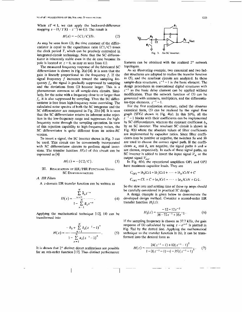
For the first realization structure, called the observer canonical form, ( 5 ) can be realized by the signal flow graph (SFG) shown in Fig. 4(a). In this SFG, all the z-' - 1 blocks with their coefficients can be implemented by SC differentiators, whereas the constant coefficient 6, by an SC inverter. The resultant SC circuit is shown in Fig. 4(b) where the absolute values of filter coefficients are implemented by capacitor ratios. Since filter coeffi- cients may be positive or negative, the switches Sa and Sb are used to choose the correct signal path. If the coeffi- cients an and bn are negative, the signal paths b and w are chosen, respectively. In each of these signal paths, an SC inverter is added to invert the input signal V,, or the output signal Vout.
In Fig. 4(b), the operational amplifiers OP1 and OP2 have maximum capacitor loads. They are
CO,, = Ib,lCcl+ Ib,lCcl+ * * + Ib,lCcN + c A. IIR Filters CO,, = CL + c + la,lCcl+ * * . + la,lCcN + Ccl.
A z-domain IIR transfer function can be written as So the slew rate and settling time of these op amps should be carefully considered in practical IC design.
A design example is given below to demonstrate the H ( z ) = n = o (4) developed design method. Consider a second-order IIR
N
5,z-n
N transfer function H,(z): 1-
n = l
Applying the mathematical technique [12], (4) can be - 12+ 122Y2
3 8 - 7 2 ~ ~ ' + 3 5 Y 2 H I ( 4 =
transformed into If the sampling frequency is chosen as 37.7 kHz, the gain response of (6) calculated by using z = eJwT is plotted in Fig. 5(a) by the dotted line. Applying the mathematical technique to the transfer function in (61, it can be trans- formed into the desired form as
N - b o + bn(z- ' - l ) "
( 5 ) n = l
H ( Z ) = N 1 - an( 2-1 - 1)"
n = l 24( 2 - l - 1) + 12( 2-' - 1)'
1 -2(z-' -1) - ( -35)(z- ' -1)2 *
It is shown that 2" distinct direct realizations are possible H ( Z ) = (7) for an nth-order function [171. Thus distinct performance

1234 IEEE TRANSACTIONS ON CIRCUITS AND SYSTEMS, VOL. 37, NO. 10, OCTOBER 1990
(b)
(SFG). (b) The SC circuit structure. Fig. 4. Observer canonical form of IIR filters with the SC differentiator as a basic element. (a) The signal flow graph
Matching t& coefficients of ( 5 ) to those of (7), we have
With thesle coefficients, the circuit is realized from that of Fig. 4(b) and shown in Fig. 5(b). The capacitance values are determined and listed in the same figure. SWITCAP 1181, [19] simulation results are plotted in Fig. 5(a), which bhow a good consistency with theoretical cal- culation resvlts.
To experwentally verify the operation of the realized IIR filter, a test chip was designed to implement the filter. This hip was designed in analog gate-array style and fabricaLd by 3.5-pm p-well CMOS technology with
photomicrograph of the fabricated 6, where the unit capacitors, trans-
mission gate arrays, and op amp arrays are indicated. The measured filter response is also shown in Fig. 5(a). Good agreement substantiates the design algorithm.
In the circuit structure of observer canonical form, all multiplications are performed simultaneously. As a conse- quence, the time taken to process one filter cycle can be as short as the time to perform one multiplication. In addition, the coefficients a , 2nd b, of (5 ) are composed of the coefficients ii,, and b, of (4). So this observer canonical structure with 2-l - 1 elements has lower coef- ficient sensitivities than the observer canonical structure with 2- l elements.
Alternatively, the transfer function of (5) can also be realized by using the observability canonical form [20] whose structure is shown in Fig. 7(a). The relations be- tween the coefficient d , in Fig. 7(a) and the coefficient b,

YU et al.: REALIZATIONS OF IIR/FIR AND N-PATH FILTERS
- - 1
- a1 - a2
1 - a , 1 0
1 . . . - a 1 1 - ...
an- , an-2 -
- a n - a n - , . . . - a 2 - a , 1 - -
1235
- 1
- a1 - a2
1 - a , 1 0
1 . . . - a 1 1 - ...
an- , an-2 -
- a n - a n - , . . . - a 2 - a , 1 -
...... + : EXPERIMENTAL 0 : SWITCAP
- 10 1 , . '0, 4 ' 6
10 1 E3 1 E4 1E5
Frequency f (Hz)
(a)
C1'9.6PF T '1 92
tbi Fi 5 (a) Theoretical, measured, and simulated frequency res onses.
fb) The SC circuit diagram of the fabricated second-order IIR &er.
On the other hand, the coefficient a, in Fig. 7(a) is the
1
J +OP AMPS
1 I -Capacitor I Array
,- Transmission Gates
-I
PADS
CircGts of Fig. 5 (a) and Fig. 12
Fig. 6. Photomicrograph of the test chip.
same as the coefficient a,, of (5). Because each coefficient d, is composed of the forward coefficients b,'s of (5), the transfer function of observability canonical form has a lower sensitivity to the variations of forward coefficients than the observer canonical form.
The other two realization methods to be considered here are of the ladder realization. They are the controller ladder and the observer ladder structures as shown in Fig. 7(b) and (c), respectively. The coefficients of these struc- tures can be directly calculated by using the similar method [21] with z-' - 1 elements in the modified trans- fer function of (5) rather than z-' elements in the trans- fer function of (4). Note that the two realized ladder structures still retain their well-known ultra-low compo- nent sensitivity, which is much smaller than the two canonical structures described above.
A design example is given below to demonstrate the filter realization using the observer ladder form. The transfer function of a third-order Butterworth low-pass filter is
1 H A S ) = (9)
(;l3+2( ;12+2( ;) + 1
where wo = 2 d l kHz). Applying the bilinear transforma- tion s = (2/ TX1- z - l / l + z-') to (9) yields the follow- ing z-domain transfer function:
H ( z ) =
8 12 6 2 1 - + - ( z - l - i ) + - ( z - l - i ) +-(z-1-1)3 8 8 8 8 - -
84 1463 8 8
l - - ( z - ' - l ) - ( -- 4 r ) ( z - 1 - 1 ) - -(z-1-1)3 *
( 10)
The SFG of this z-domain transfer function is given in Fig. 8(a), and the values of coefficients c, and d, are also given in the figure. The resultant SC ladder realization is shown in Fig. 8(b), where the capacitor values are also given and the sampling frequency is 37.7 kHz. Suitable

1236 IEEE TRANSACTIONS ON CIRCUITS AND SYSTEMS, VOL. 37, NO. 10, OCTOBER 1990
Fig4 7.
d E’- 1
Y
X
(C)
Three distinct signal flow graphs (SFG’s) of an IIR transfer function with the SC differentiator as a basic (a) The observability canonical form. (b) The controller ladder form. (c) The observer ladder form.
scaling has been applied to determine the values of those capacitors in Fig. 8(b) so that the filter coefficients a , and b,, of (10) dan be realized exactly and so the capacitor values have I an adequate spread. The SWITCAP simula- tion results bf this observer ladder type of IIR filters are given in Fib. 8(c). It can be seen from Fig. 8(c) that SWITCAP dimulation results are in good consistency with theoretical qalculation results.
It is known that there are many possible structures with different p rformance features for a given IIR filter transfer fu ction. Based upon the developed design methodolo and the differentiator-type elements 2- l - 1, other netw rk topologies besides the demonstrated four structures, ch as cascade, parallel, direct, direct canonic, ladder, wav 1 , or combinations of them can also be used to realize the transfer function of (5).
element.
Just like the LCR ladder filters designed by using SC integrators, the realized IIR filters using SC integrators with l / (z - ’ - 1) basic blocks have a dc instability prob- lem [6] in some cases such as some bandpass and high-pass IIR filters. Thus dc feedback path checking and circuit structure modification [6] are required before a stable SC-integrator-based IIR filter could be obtained. In real- izing those IIR filters using the proposed SC differentia- tor-based circuits, however, the “ return-to-zero” sampling type completely eliminates this dc instability problem. This is a significant advantage of the proposed IIR filters over the conventional SC-integrator-based structures. The other advantage is that the SC-differentiator-based IIR filters have a lower component sensitivity than the SC- integrator-based structures. This will be proved in the following subsection. In addition, these SC-differ-

YU et al.: REALIZATIONS OF IIR/FIR AND N-PATH FILTERS 1237
d3 = 2 6 0 I 1 1
Gain(dB) 0 ,
lo= lKHa f S I
-40-
SWITCAP slrnulaled results of
-80- lheorelocal colculotmons of Eq (IO)
-120 0.1K 1K 10K 1CQK
(C) Fig. 8. A third-order observer ladder form of a low-pass IIR filter with the SC differentiator as a basic element. (a) The
signal flow graph. (b) The resultant SC circuit structure. (c) The SWITCAP simulated frequency responses with the theoretical calculations.
1238 IEEE TRANSACTIONS ON CIRCUITS AND SYSTEMS, VOL. 37, NO. 10, OCTOBER 1990
(b) Fig. 9 . (a) The signal flow graph. (b) The resultant SC circuit diagram of an FIR filter.
entiator-based IIR filters retain the inherent advanta- can be characterized bv
( 13) geous performance of the SC differentiator that has been H ( Z ) = f(Y' - l , b , , b,, * * . ) described in Section 11.
where b,, b,, . . are the multiplier constants. The sensi- B. FIR Filters tivities of this network topology are given by [22]
An FIR filter can be characterized by the z-domain
N -
aH(z ) D E ( z ) = -
transfer function ab, = (multiplier input)original( multiplier input),djOint
(11) = (2-1 - I ) , . ( 14) H ( z ) = bnz-". n = O
If the z-domain transfer function of (11) is directly implemented by a similar structure with the delay ele- ments z - l , the sensitivity of this circuit to the variations of multiplier constants can be obtained as
Applying t h above-developed mathematical technique, this polynomial form can be transformed into the form
N
H ( z ) = b,(z-' -1)". (12) n = O
2) DC( 2 ) = v ab, = ( 2 - q
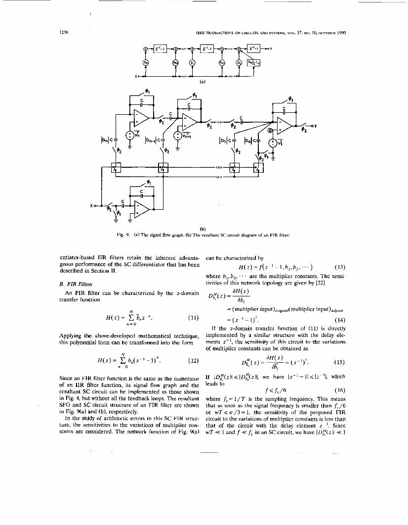
Since an FIR filter function is the same as the numerator of an IIR filter function, its signal flow graph and the resultant SC circuit can be implemented as those shown in Fig. 4, but without all the feedback loops. The resultant SFG and SG circuit structure of an FIR filter are shown in Fig. 9(a) and (b), respectively.
In the study of arithmetic errors in this SC FIR struc- ture, the sensitivities to the variations of multiplier con- stants are considered. The network function of Fig. 9(a)
If lD:(z)l G ID[(z)l, we have 1z-l - 11 G Iz-lI, which leads to
where fs = 1/ T is the sampling frequency. This means that as soon as the signal frequency is smaller than f,/6 or w T g a / 3 = 1 , the sensitivity of the proposed FIR circuit to the variations of multiplier constants is less than that of the circuit with the delay element z-I . Since wT -=z 1 and f << f, in an SC circuit, we have lD[(z)I e 1
f G fs/6 ( 16)

YU et al.: REALIZATIONS OF IIR/FIR AND N-PATH FILTERS 1239
and IDb’f(z)l a lD{(z)l. Under the same consideration, one can obtain the conclusion that the normalized sensi- tivity functions Sb’f = $Db’f has a much smaller magnitude than Sf. In view of the sensitivities of this circuit to the variations of multiplier constants, the proposed SC FIR circuit is superior to other circuits implemented by the delay element 2- l .
The above sensitivity analysis can be also applied to the IIR filters. It is shown that the realized IIR filters with SC differentiators have much lower component sensitivi- ties than the SC-integrator-based IIR filters. This is be- cause the values of 1z-l- ll in SC-differentiator-based structures is much lower than those of Il/(z-’ - 1)1 in SC integrator-based structures. Although conventional SC in- tegrators can be used to realize IIR filters, they cannot be applied to realize FIR filters directly using the above described design technique.
As in other analog filters, the noise leads to a funda- mental limitation on the dynamic range. Because the dominant noise source of an SC differentiator is the equivalent thermal noise [41, only the equivalent input thermal noise of op amps is considered in analyzing the noise effect of the FIR structure. Assume the mean square value of an equivalent noise source at the input of the ith op amp is as shown in Fig. 9(b). Since all the noise sources are uncorrelated, the total equivalent noise appearing at the input node B of the last op amp in this SC FIR filter can be determined as
i = l - - -
where Ai = 1z-l- 11’-l. Assuming - V,’= V,’-l= = v:, the equivalent noise source V , can be rewritten as
- - v;= v;[ ( 1 2 - 1 - 112” - 1)/( 12-1 - 112 -
Note that the value 1z-l- 11 has a maximum value 6 when the spectra frequency of the equivalent thermal noise is equal to fs/2. Thus (18) has a maximum value of
- - v;(max) = V,”( 2” - 1). (19)
The equivalent input thermal noise of an op amp is usually in the range of 4 to 60 nV/& [231, so the maximum value of the equivalent noise is only 4 mV/\/Hz when the stage number n of the SC FIR filter is as large as 32. If the maximum output swing is +5, a dynamic range over 60 dB can be obtained in the last op amp.
In usual applications, the signal frequency is much lower than the sampling frequency f,. Thus this maximum equivalent noise source of the FIR filter at f,/2 can be easily removed by using an adequate post filter. More- over, through an adequate design procedure and/or good process technique, a low noise op amp can be designed to increase the maximum number of stages and/or the dy- namic range of this SC FIR filter.
A linear-phase low-pass FIR filter is designed in the following example by using the proposed FIR structure.
The transfer function in the jw-domain is
otherwise
where ws is the sampling angular frequency, aT is the group delay, and w, is the center frequency. The corre- sponding impulse response is
- sinw,(n - a) b; = n # a.
Clearly, 5,: has an infinite duration. To create a finite duration linear-phase FIR filter of the length N = 10, we choose the Hanning window w(n) = 1/2[1- cos(2.rrn / N - 111. Then, 5, can be obtained as
$,=b;*w(n), O < n < N - 1 = 9
sinw,(n-a) [ ( 2 m ) ]
. rr(n-a) ’
1-cos - - - 2 4 n - a) N - 1 ’
= ( N - 1)/2 = 4.5.
The numerical values of $A, b,, b,, and the truncated numbers of 5, and b,, are listed in Table I. The gain and phase responses are calculated and shown in Fig. 10(a) and (b), respectively. As shown in Fig. lMa), the passband width of this filter is defined as the center frequency f , plus the mainlobe transition width of the gain response, which is approximately (1/20) + (2/10)f, = (1/4)fs. SWITCAP simulation results with both exact b,, and truncated b, coefficients are also shown in Fig. 10(a) and (b), respectively, where the consistency with theoretical calculation results is quite good, especially in the pass- band.
From both theoretical calculations and SWITCAP sim- ulations, it is seen that this circuit is a good linear-phase filter. The group delay from SWITCAP simulation results is 4.5T (T = 100 ps) consistent with the theory. The dc gain of the filter can be adjusted through the feedback capacitor C of the last op amp in Fig. 9(b).
Since the realized FIR filters make use of SC differen- tiators directly, they all have the advantageous features of SC differentiators as mentioned in Section 11. As com- pared with other FIR filters [13]-[16], the proposed struc- ture is simpler and more concise whereas the design method is easy. This makes the structure quite attractive in many VLSI applications.
(17)
IV. MULTIPLEXING TECHNIQUE AND
N-PATH CIRCUITS A. Multiplexing Technique
For the proposed SC differentiator, the multiplexing technique can be developed to allow some op amps servic- ing many filter channels at a time.
Fig. l l(a) shows the basic multiplexing structure for the proposed SC differentiator circuit. Their control clocks are plotted in Fig. ll(b). As may be seen from Fig. 11, the period of all internal clock signals - bN is NT and each clock is successively shifted by T. On the other hand,

1240 IEEE TRANSACTIONS ON CIRCUITS AND SYSTEMS, VOL. 37, NO. 10, OCTOBER 1990
4 0.099589213524 0.09658628948 3.62883759458 0.097
TABLE I NUMERIC VALUES OF &;,&,, b,, TRUNCATED E,, AND TRUNCATED b,
0.43103821256 0.430
3.914
3.587
I I I I I 3 0.096339776200 0.07225483215 4.70234973824 0.072 4.669
5 0.099589273524 0.09658628948 1.84212087273 0.097 1.810
0.583
0.109
0 f 009
the clock C$ has a period of T and is nonoverlapping to other clocks. It can be easily shown that the output transfer fundtions in the z-domain are
where
z = exp (sNT).
Thus N SC differentiators can be implemented by using only one op amp.
The above multiplexing technique can be applied to the design of filter banks. As a demonstrating example, two second-order IIR filters are designed using the developed method. One of the filter transfer functions is given in (6). The other isigiven below:
- 12+ 12t -2 H2(Z) = 37-72z-l +35z-2 * (21)
Using the design algorithm in Section 111-A, H 2 ( z ) can be similarly realized. Then the two filters are merged by using the abwe developed multiplexing method. The real- ized filter is shown in Fig. 12(a). The control clocks 4l and C$2 have a frequency of 37.7 kHz and their timing diagrams ar$ plotted in Fig. 12(b). The filter bank was fabricated by using the 3.5 p m analog CMOS process. The measusd response of one of the fabricated IIR filters (H,(z) ) is shown in Fig. 5(b), whereas that of the
other IIR filter (H2(z)) is shown in Fig. 13. Good agree- ment among theoretical calculations, SWITCAP simula- tions, and measured results confirms the correctness of the proposed multiplexing method.
Unlike the case in the multiplexed SCF banks using SC integrators [7], the proposed multiplexing technique using SC differentiators does not require any modification of the original differentiator structure. Thus the resultant multichannel filter bank retains all the advantageous fea- tures of the original SC differentiator-based filters as mentioned in Sections I1 and 111.
In a filter bank consisting of N filter channels, only one-Nth of op amps is required as compared to the conventional filter structures. But the control clock fre- quency of each op amp is N times higher than that in the conventional structure. For voice-band CMOS op amps, N times of increase in clock operation frequency still can be achieved without N times of increase in power dissipa- tion. In this case, the filter bank can save the dc power consumption. As to the chip area, however, it should be noted that like all other multiplexed SCF banks, the saved op amp area might be outweighed by additional clock buses, clock drivers, and interconnection lines.
B. N-Path Filters The multiplexed SC differentiator shown in Fig. l l(a)
can be modified to form a basic-type N-path circuit. This is done by choosing C2 = C 3 = . . . = C N = C 1 in Fig. ll(a) and merging all the output terminals to form a single output and all the input terminals to form a single input. The resultant circuit structure is shown in Fig. 14(a) where the internal clock signals are the same as those in Fig. l l(b) and repeated in Fig. 14(b). It is evident that the function of the circuit of Fig. 14(a) is similar to that of Fig. l(a), except that each input capacitor C1 is

YU et al.: REALIZATIONS OF IIR/FIR AND N-PATH FILTERS 1241
Gam(d0) 0 I 1 I I
SWITCAP with b
-80-
frequency (a)
Phase (degree)
7-
frequency - (b)
Fig. 10. An example FIR filter. (a) The gain. (b) The phase responses.
(a)
L N T _I
operated by an NT-period clock, rather than a T-period clock.
If all signal paths are identical, they have the same transfer functions as
where
z = exp ( s N T ) . Since every signal path is activated within a single period T and left open for the other ( N - 1 ) T periods, the transfer functions in (22) can be reexpressed as
where
where
z , = exp ( s T ) = ~ ' 1 " .
The z-plane pole/zero pattern of Fig. 15(a) can be trans- formed into the 2,-plane pattern shown in Fig. 15(b) for N = 3. In the following example, a narrow-band bandpass filter is designed by using this basic-type N-path struc- ture.
Applying the bilinear transformation s = 2(1- z - ' ) / T(1+ z - ' ) to the analog transfer function in (9) yields the following z-domain transfer function:
H ( 2 )
(b)
form diagram. Fig. 11. (a) Multiplexed SC differentiator circuit. (b) Its clock wave- where = exp(sT)' the center frequency fo is 6o Hz' and
the sampling period T is 1/1508 s. Using the design

~
1242
2o
.-. $ 10- v
- - 5 .
IEEE T R A N S A ~ I O N S ON CIRCUITS AND SYSTEMS, VOL. 37, NO. 10, OCTOBER 1990
fc = 1 KHz t
.e d '
6 'P
37.7KHz
0:SWlTCAP
: THEORETICAL
6 + : EXPERIMENTAL
6 6
6
d
(b) Fig. 12. (a) Circuit diagrams and (b) clock waveforms of two multiplexed SC-differentiator-based IIR filters.
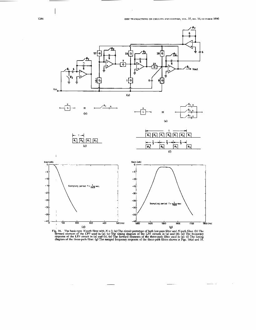
algorithm in Section 111-A, (25) can be realized. The resultant SC low-pass filter (LPF) prototype is shown in Fig. 16(a) and its component spread can be minimized through an adequate weight. The forward element G and the clock wpveforms are shown in Fig. 16(b) and (c). The SWITCAP simulation results are shown in Fig. 16(d).
Now, changing the forward element G and the clock waveforms to those shown in Fig. 16(e) and (f), respec- tively, the resultant transfer function of this basic-type N-path circuit ( N = 3) becomes
H ( 2)
where
z,=exp s- =z1I3. ( T i In this three-path bandpass filter, the center frequency of the bandpass filter becomes 1508 Hz, and the passband is in the range of 1508 f 60 Hz as shown in Fig. 16(g). Note that the center frequency of the bandpass filter response is just the sampling frequency of each LPF and the bandwidth af this N-path circuit is 120 Hz. The loss at the passband e$e is due to the sample-and-hold effect, which is about - 1.68 dB.
If the basic-type N-path SC differentiator circuits are used to build an N-path circuit like that of Fig. 14(a), the inevitable mismatches among the forward capacitors
I d
I I I .P,l,,, I I , , , , , , I , , , 1 , I , , , I , , , , ,,, 10 100 1E3 1 E4 11
Frequency f (Hz) Fig. 13. The frequency responses of the IIR filter shown in Fig. 12
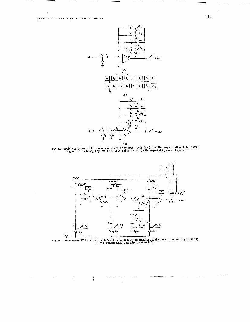
(Cl's) and the multiplexing switches are sufficient to introduce a noise at the center of passband [9]. To solve this problem, the uniformity among signal paths must be enforced. This can be done by using a single forward capacitor C1 for all the signal paths. Meanwhile the signal charges are stored on the added extra capacitors when they are not processed in the circuit. Thus a RAM- type [91 N-path differentiator circuit can be formed as shown in Fig. 17(a) where C is the common feedback capacitor shared by all paths, and Csi is the storage capacitor used for the path i. The timing diagram is

YU et al.: REALIZATIONS OF I I R / F I R AND N-PATH FILTERS 1243
NT - 'n*(N-l)T h.(N-l)T+NT
(b)
basic-type SC-differentiator-based N-path circuit. Fig. 14. (a) The circuit diagram and (b) its clock waveforms of a
shown in Fig. 17(b). The operations of this RAM-type N-path circuit are described below.
During the period of the clock 44 (and the clock 42), the charge Cll/,,(tn-T) on the capacitor C1 is transferred into C,, and the charge on the feedback capacitor C is discharged to zero. The charge on C,, remains unchanged until the clock 43 (and the clock 4,) is activated after a full cycle. Then the charge CIVin(tn-T) of C,, is trans- ferred back into C. Since C1 is connected to Vi, at the same time, the charge ClK,(t,) on C l also appears on C through induction. Thus the net change of charge on C is - Cl[Vin(t,>- Vin(tn-T)l at the end of the clock 43 (and the clock 4,). The same operation is performed during the other clock periods (45,46) and (&,&I. Thus the overall transfer function is given by
where
z,=exp s- = z ' / ~ . i Ti A delay element can be implemented by using this
RAM-type N-path circuit. The circuit is shown in Fig. 17(c) and the timing diagram is the same as that in Fig. 17(a). The overall transfer function of this delay element can be expressed as
where
z,=exp s- =P3. i :I
I Z - Plane
(b) Fig. 15. (a) Pole and zero locations of the SC differentiator in Fig.
l(a). (b) Pole and zero locations of the multiplexed SC differentiator in Fig. 14(a) with N = 3.
As an illustrating example, (26) is implemented by using the RAM-type N-path circuit. First the transfer function in (26) is rewritten as
H ( ZU)
2 1
2 399
1 3 z i 3 + -( 2 z i 3 - 1) + - ( z i 3 4 - 1) + - ( z i 3 8
- 99
- - - 13
I--( 2 za - 3 4 ) - - 4 ( 2u -"i) --(z;3-1)3 8
Z a - Plane Z a r exp(ST)
where
z ,=exp(sT).
In (30), the block of z i 3 - 1 can be implemented by the circuit of Fig. 17(a) and the block of 2 i 3 by the delay element of Fig. 17(c). The resultant RAM-type N-path circuit is shown in Fig. 18, where the clocks are all indicated beside the switches without the parentheses. The feedback branch I; and the timing diagram can be found from Fig. 17(a) and (b), respectively. Note that this RAM-type N-path circuit uses fewer op amps than the basic N-path structure of Fig. 16(a). Moreover, as men- tioned earlier, this N-path circuit is less susceptible to noise at the center frequency as compared to the N-path circuit of Fig. 16(a). The simulation results are shown in Fig. 16(g) also. It can be seen that the response is very consistent with the basic-type N-path circuit of Fig. 16(a).
1244
-401 ! * 0 , 100 200 300
-10-
-15-
-20 -
-25 -
-30 -
-35 -
-4d
IEEE TRANSACTIONS ON CIRCUITS AND SYSTEMS, VOL. 37, NO. 10, OCTOBER 1990
Vin A I I
(a)
Gain (d8) 0 ,
1245 YU et al.: REALIZATIONS OF IIR/FIR AND N-PATH FILTERS
vout
f f
(a)
(C)
Fig. 17. RAM-type N-path differentiator circuit and delay circuit with N = 3. (a) The N-path differentiator circuit diagram. (b) The timing diagrams of both circuits in (a) and (c). (c) The N-path delay circuit dlagram.
Fig. 18.
Vin 1 1. 1 J
An improved SC N-path filter with N = 3 where the feedback branches and the timing diagrams are given 0
17 or 19 and the realized transfer function of (30). in Fig.

1246 IEEE TRANSACTIONS ON CIRCUITS AND SYSTEMS, VOL. 37, NO. 10, OCTOBER 1990
- . - (C)
Fig. 19. Circ latin delay N path differentiator circuit and dela cir cuit with N E 3. ($The N-path differentiator circuit diagram. (bYThe timing diaghms of both circuits in (a) and (c). (c) The N-path delay circuit diagrbm.
Based on the similar principle in circulating-delay N - path SC integrators [9], a circulating-delay N-path SC differentiatbr can also be constructed as shown in Fig. 19(a) for N = 3. Its timing diagram is shown in Fig. 19(b). The operation is described in the following. When the clock is on, the stored charge CIK, , ( fn -T) of C,, is transferred into the feedback capacitor C. Meanwhile the charge ClV#,) on C1 appears on C through induction. Thus the net charge on C is - Cl[V,,(t,)- V,n(t ,-T)] at the end of the clock 41. When the clock 42 is on, the charge on C,, is transferred to C,, and the voltage on the feedback clpacitor C is discharged to zero. During the period 43 1, the charge on C,, is transferred to Cs2. During the period 44 = 1, the charge ClV,,(t,) on C1 is transferred to CS3. When 41 = 1 again, the above cycle is then repeaqed. Clearly, it requires N ( N + 1) = 12 clock phases to pqrform a full cycle of operation.
From the above description, it is evident that the circuit of Fig. 19(a)l has the same transfer function as that of Fig. 17(a), and qach stored charged packet is in the memory for a T peripd. Hence the overall transfer function of the SC differentiator of Fig. 19(a) is the same as (28). A delay element of ' the circulating-delay N-path circuit is also shown in Fib. 19(c), and the transfer function is given by
(29). Using the circuiting-delay N-path circuit to imple- ment (301, the resultant circuit structure is the same as that of Fig. 18 except that the clocks are those shown in the parentheses beside the switches and the feedback branches F , and the timing diagrams are shown in Fig. 19(a) and (b), respectively. The simulation results are shown in Fig. 16(g), where the responses are exactly consistent with those of the basic-type and the RAM-type N-path circuits.
It should be noted that various designs of low-pass SC prototype filters can also be applied in the synthesis of basic-type, RAM-type, or circulating-delay-type N-path filters. Gengfally, the RAM-type or the circulating-delay- type N-path filter has less noise effects at the center frequency of passband than the basic-type N-path filter. The voltage gain of the op amps in the RAM-type circuit can be lowered by a factor of four [91 over that in the circulating-type circuit. But the RAM-type circuit needs eight clock signals, twice as many as the circulating-delay type circuit.
Both SC differentiator- and SC integrator-based N-path filters have several common problems, such as the clock feedthrough effect, the open-loop mode of the op amps, and the noises generated from switches and op amps. These problems must be considered in practical design and are worth a deeper analysis. Because all N-path filters generate mirror frequency noise [9] by reflecting the low-frequency noise to the sampling frequency and the basic SC-differentiator-based low-pass prototype filter has a low noise in the low-frequency range, the resultant N-path circuit is expected to have a low mirror frequency noise. From this point of view, they are superior to the conventional SC-integrator-based N-path circuits.
V. CONCLUSION A novel design methodology has been successfully de-
veloped for the realization of IIR filters, FIR filters, multiplexed filter banks, and N-path filters using SC differentiators. All the realized circuits have been verified through SWITCAP simulations. Part of them were fabri- cated in analog CMOS process and the measured results have shown a good consistency with the simulation re- sults.
The IIR and FIR filters as well as the multiplexed filter banks use the SC differentiators directly without modifi- cations. As compared to the conventional SC-integrator- based design, the proposed IIR filters have a lower com- ponent sensitivity and are free from the dc instability problems whereas the proposed N-path filters have a better noise performance. For the analog FIR filters that cannot be realized directly by using SC integrators, they have a simpler and more compact structure with a better performance as compared to other analog FIR filters. Except for these distinct features, all the proposed filter circuits retain other advantageous performance of SC differentiators as well, such as stray insensitive structures, low sensitivity to offset voltage and power supply varia- tions, maximum output swing, and low noise in the low-
-

1247 YU et al.: REALIZATIONS OF IIR/FIR AND N-PATH FILTERS
frequency range. In conclusion, the inherent good perfor- mance and the compact structure of the realized filter circuits using SC differentiators make their applications in signal processing quite promising and feasible.
REFERENCES B. J. Hosticka and G. S. Moschytz, “Practical design of switched- capacitor networks for integrated-circuit implementation,” IEE J. Electron. Circuits Syst., vol. 3, pp. 76-88, Mar. 1979. F. Montecch;,, ,“Bilinear design of high-pass switched-capacitor ladder filters, in Proc. IEEE Int. Symp. Circuits and Systems, pp.
Y. Horio and S. Mori, “SC modified lossless discrete differentia- tors and resulting SC highpass ladder filters,” Electron. Lett., vol. 22, pp. 97-99, Jan. 1986. C.-Y. Wu, T.-C. Yu, and S. S. Chang, “New monolithic switched- capacitor differentiators with good noise rejection,” IEEE 1. Solid-State Circuits, vol. 24, Feb. 1989. -, “Realization of FIR and IIR filter using SC differentiators,” in Proc. Symp. on W S I Circuits, Japan, pp. 99-100, 1988. C.-Y. Wu and T.-C. Yu, “The design of biqdads, high-pass, and band-pass ladder filters using switched-capacitor differentiators,” submitted to IEEE J. Solid-state Circuits. P. W. Bosshart “A multiplexed switched capacitor filter bank,” IEEE J. Solid-&ate Circuits, vol. SC-15, pp. 939-945, Dec. 1980. L. E. Franks and I. W. Sandberg, “An alternative ap roach to the realization of network transfer functions: The N-pat! filter,” Bell Syst. Tech. J . , pp. 1321-1350, Sept. 1960. M. B. Ghaderi, J. A. Nossek, and C. C. Temes, “Narrow-band switched-capacitor bandpass filters,” IEEE Trans. Circuits Syst.,
S. K. Mitra. M.-A. Kofi, and K. Hirano, “Theov and applications
547-550, 1985.
vol. CAS-29, pp. 557-572, Aug. 1982.
of all-digital N-path filters,” IEEE Trans. Circ& Syst.,. vol. CAS- 34, pp. 1045-1052, Sept. 1987. R. Gregorian, K. W. Martin, and G. C. Temes, “Switched-capaci- tor circuit design,” Proc. IEEE, vol. 71, pp. 941-965, Aug. 1983. A. M. Davis and R. R. Smith. “Desien of state-variable SC filters
D. Von Grunigen, U. W. Brugger, and G. S. Moschytz, “Switched-capacitor frequency-sampling N-path filtef.,” in Proc. IEEE Int. Symp. Circuits and Systems, pp. 209-212,,bfay 1982. N. S. Reddy and M. N. S. Swamy, “Switched-capacitor realization of FIR filters,” IEEE Trans. Circuits Syst., vol. CAS-31, pp. 417-423 Apr. 1984. Y.-S. Lek and K. W. Martin, “A switched-ca acitor realization of multble FIR filters on a single chip,” IEEE l! Solid-Stare Circuits, vol. 23, pp. 536-542, Apr. 1988.
[17] A. Antoniou, Digital Filters Analysis and Design. New York: Mc- Craw-Hill, 1979.
[18] S. C. Fang, Y. P. Tsividis, and 0. Wing, “SWITCAP: A switched- capacitor network analysis program-Part I,” IEEE Trans. Circuits Syst., vol. CAS-30, pp. 4-10, Sept. 1983.
[19] -, “SWITCAP: A switched-capacitor network analysis pro- gram-Part 11,” IEEE Trans. Circuits Syst., vol. CAS-30, pp. 41-46, Dec. 1983.
[20] T. Kailath, Linear System. Englewood Cliffs, NJ: Prentice-Hall, 1980.
[21] S. K. Mitra and R. J. Sherwood, “Digital ladder networks,” IEEE Trans. Audio Electroacoust., vol. AU-21, pp. 30-36, Feb. 1973.
[22] R. E. Soviora and M. Sablatash, “A Tellegem’s theorem for digital filters,” IEEE Trans. Circuit Theory, vol. CT-18, pp. 201-203, Jan. 1971.
[23] Y. Tsividis and P. Antognetti, Design of MOS VLSI Circuits for Telecommunications. Englewood Cliffs, NJ: Prentice-Hall, 1985.
rEc Tsai-Chung Yu, photograph and biography not available at time of publication.
rEc Chung-Yu Wu (S’76-M’88), photograph and biography not available at time of publication.
by means of polynomial transform&on,” IEEE Trans. Circuits Syst., vol. CAS-33, pp. 1248-1251, Dec. 1986. T. Enomoto, T. Ishihara, and M.-A. Yasumoto, “Integrated tapped MOS analogue delay line using switched capacitor Electron. Lett., vol. 18, pp. 193-194. Mar. 1982.
Shin-Chi C h a w photograph and biography not available at time of publication.