ieee transactions on power electronics, …pgembeddedsystems.com/securelogin/upload/project/... ·...
TRANSCRIPT
IEEE TRANSACTIONS ON POWER ELECTRONICS, VOL. 27, NO. 3, MARCH 2012 1383
High Step-Up DC-DC Converters UsingZero-Voltage Switching Boost Integration Technique
and Light-Load Frequency Modulation ControlHyun-Wook Seong, Student Member, IEEE, Hyoung-Suk Kim, Student Member, IEEE, Ki-Bum Park, Member, IEEE,
Gun-Woo Moon, Member, IEEE, and Myung-Joong Youn, Senior Member, IEEE
Abstract—This paper describes nonisolated high step-upDC-DC converters using zero voltage switching (ZVS) boost inte-gration technique (BIT) and their light-load frequency modulation(LLFM) control. The proposed ZVS BIT integrates a bidirectionalboost converter with a series output module as a parallel-input andseries-output (PISO) configuration. It provides many advantagessuch as high device utilization, high step-up capability, power andthermal stress distribution, switch voltage stress clamping, andsoft switching capability. As an example of ZVS BIT, a flybackconverter with a voltage-doubler rectifier (VDR) as a series out-put module is presented and analyzed in detail. In addition, toovercome the efficiency degradation at a light load due to the load-dependent soft switching capability of the proposed ZVS BIT, acontrol method using a frequency modulation (FM) proportionalto the load current is proposed. By means of ZVS BIT and LLFMcontrol, the overall conversion efficiency is significantly improved.The experimental results are presented to clarify the proposedschemes.
Index Terms—Boost integration technique (BIT), frequencymodulation (FM), step-up ratio, zero-voltage switching (ZVS).
I. INTRODUCTION
NONISOLATED DC-DC conversion applications such aselectric vehicles (EV), photovoltaic (PV) grid-connected
power systems, fuel cells, uninterruptible power supplies (UPS),and high-intensity-discharge (HID) lamps for automobile head-lamps call for high-performance step-up techniques [1], [5],[13]. The general approach to these applications is a classi-cal boost converter having simple structure, continuous inputcurrent, and clamped switch voltage stress to the output volt-age. However, the limited step-up capability due to the parasiticresistances, the reverse recovery problem caused by a high volt-age rating diode, and the large switching losses due to the hard
Manuscript received April 18, 2011; revised June 17, 2011; accepted July 13,2011. Date of current version February 7, 2012. Recommended for publicationby Associate Editor J. A. Pomilio.
The authors are with the Department of Electrical Engineering, KAIST,373-1, Guseong-dong, Yuseong-gu, Deajeon, Korea, 305-701 (e-mail: [email protected]).
This paper includes previously presented literatures titled as1. “Zero-Voltage Switching Flyback-Boost Converter with Voltage-Doubler
Rectifier for High Step-up Applications,” in ECCE 2010, Atlanta, USA.2. “Zero-voltage Switching Dual Inductor-fed DC-DC Converter for High
Power Step-up Applications,” in ECCE 2009, San Jose, USA.Digital Object Identifier 10.1109/TPEL.2011.2162966
switching are major obstacles not allowing the high step-up ratioand efficiency.
To handle these concerns, several converter topologies adopt-ing the voltage conversion ability, i.e., a voltage-multiplier, acoupled-inductor, a transformer, and a stacked output capacitor,have been proposed [1]–[23].
In [2]–[6], it has been demonstrated that a voltage-multiplierusing additional diodes and capacitors on the output stage in aclassical boost converter contributes to extending a step-up ratiowithout the penalty of an extreme duty ratio. However, as theoutput voltage is increased, the number of stages is increased,demanding more capacitors and diodes. Moreover, the snubbercircuits across the switches and diodes increase the cost, losses,and design complexity. Also, no soft switching capability stillconfines the efficiency to be low.
A coupled-inductor employed in a boost converter is also afavorable step-up technique for its simple structure [1], [7]–[12].Although it can achieve a high efficiency and protect the switchfrom the high peak voltage, an auxiliary circuit is required tosuppress the switch voltage stress. The active-clamp cell in thecoupled-inductor scheme can alleviate this problem [10]–[12].Also, it can achieve the soft switching performance. How-ever, the active-clamp cell in [10] and [11] is quite complex,requiring a pair of switches and diodes. Although the cellpresented in [12] can reduce the number of active devices, theadditional resonant inductor to guarantee the ZVS should beadopted. Besides, as the auxiliary turns of a coupled-inductorare increased to raise a step-up ratio further, an input cur-rent ripple becomes larger in return. Thus, more input filter isneeded.
Another easy approach for a high step-up ratio is the current-fed type converters using a transformer [14]–[21]. A transformerleakage inductance causes a voltage spike across the switchesso that a snubber circuit is required, resulting in an additionalloss. The active-clamp approach similar to that applied on thecoupled-inductor scheme releases these problems and reducesswitching losses by using its soft switching capability [17]–[21].
Unfortunately, in view of the clamp capacitors in [10]–[12]and [17]–[21], they are connected to the input side so that it hasno function of extending a step-up ratio.
Focused on the step-up ratio extension with the concept ofthe stacked output capacitors, the high step-up boost-flybackconverter is proposed in [22] and improved with a secondaryvoltage-doubler rectifier in [23]. Despite their high step-up ca-pability, the switch suffers from the hard switching losses.
0885-8993/$26.00 © 2011 IEEE

1384 IEEE TRANSACTIONS ON POWER ELECTRONICS, VOL. 27, NO. 3, MARCH 2012
Fig. 1. Conceptual diagram of ZVS BIT.
As a desirable solution to the abovementioned drawbacks,this paper proposes nonisolated high step-up DC-DC convertersusing a zero-voltage switching (ZVS) boost integration tech-nique (BIT). It integrates a bidirectional boost converter intoseveral isolated current-fed type converters as a parallel-inputand series-output (PISO) configuration. This connection makesthe bidirectional boost converter an active-clamp circuit whichis not connected to the input side but the output side. Therefore,it can use a high step-up capability of the stacked output ca-pacitors while maintaining the soft switching capability of theactive-clamp circuit. Furthermore, several advantages such ashigh device utilization, power and thermal stress distribution,and switch voltage stress clamping can be achieved. Since aleakage inductor alleviates di/dt of the secondary rectifier cur-rent, reverse recovery problems too can be reduced.
However, the proposed ZVS BIT has the load-dependent ZVScondition, which is an inherent characteristic of the active-clampcircuit. It causes a hard switching at a light load and degradesthe conversion efficiency. To recover the ZVS at a light load,a control method using a frequency modulation (FM) is alsoproposed, which can be applied to other active-clamp schemesto improve light-load efficiency.
The general concept and features of the proposed ZVS BITare introduced first. Then, a flyback converter with a voltage-doubler rectifier (VDR) as a series output module is proposedand analyzed in detail as an example of ZVS BIT. Next, the light-load frequency modulation (LLFM) control is presented. Also,other converters derived from the ZVS BIT are proposed andsummarized. The experimental results are presented to verifythe proposed schemes.
II. ZERO-VOLTAGE SWITCHING BOOST
INTEGRATION TECHNIQUE
Fig. 1 shows the conceptual diagram of ZVS BIT. A seriesoutput module is connected to a bidirectional boost converteras a PISO configuration. This series output module can be anyisolated current-fed type converter. Also, it can adopt any kindof secondary rectifiers such as the full-bridge, center-tapped,voltage-doubler, and so on. For an easy understanding of theproposed ZVS BIT, an example using a flyback converter as aseries output module is introduced as shown in Fig. 2.
Fig. 2. Derived ZVS flyback-boost converter: (a) Flyback converter as a seriesoutput module. (b) Key waveforms.
A. High Device Utilization
To increase the device utilization and simplify the circuit, thecommon parts integration between a series output module and abidirectional boost converter is recommended. Fig. 2 shows anexample of the common parts integration. As shown in Fig. 2(a),a bidirectional boost converter and a flyback converter can beintegrated easily since the boost inductor LA and switch Q1 inFig. 1 become the flyback converter counterparts.
B. High Step-up Capability
Due to the stacked output capacitors, each output capacitorvoltage is added and the overall output voltage can be extendedas
VO = VC O1 + VC O2 . (1)
That is, the output voltage of the converters employing the pro-posed ZVS BIT is a sum of the output voltages of the boostconverter and the series output module, which is suitable forhigh step-up applications.
C. Power and Thermal Stress Distribution
By imposing the node equations on the output capacitor CO 2 ,the steady-state output current equation can be derived as
IO = 〈IA (t)〉 = 〈IB (t)〉 (2)
where 〈•〉 denotes the average value of •. Equation (2) impliesthe power distribution between the bidirectional boost converterand the series output module is proportional to each outputvoltage. Therefore, the thermal stress can be decentralized.

SEONG et al.: HIGH STEP-UP DC-DC CONVERTERS USING ZERO-VOLTAGE SWITCHING BOOST 1385
Since the same average current flows through each outputcapacitor, the current distribution at the primary side is alsopredictable and can be expressed as follows:
n〈IIN A (t)〉 = 〈IIN B (t)〉. (3)
That is, the current distribution ratio at the powering phase onlydepends on the transformer turns ratio n, which decides the slopeof the primary current Ipri(t) while Q1 is turned off. It is notedfrom Fig. 2(b) that the powering current distribution depictedby the diagonal-lined and vertical-lined areas satisfies (2) and(3).
D. Switch Voltage Stress Clamping
The switch voltage stresses VQ 1 and VQ 2 can be clampedto the partial output voltage VC O 1 . Thus, additional protectioncircuit for the high voltage spike caused by a leakage inductorLlkg is not required.
E. Soft Switching Capability
The proposed ZVS BIT seems to be an active-clamp network,which is not connected to the input side but the output side.The previous works regarding the active-clamp circuit concen-trate on the soft switching capability and switch voltage stressclamping [10]–[12], [17]–[21]. However, the proposed ZVS BITprovides these abilities as well as the step-up ratio extension be-cause of the series output connection of the clamp capacitorCO 1 .
The soft switching characteristics are similar to the active-clamp circuit. A main switch Q1 has a load-dependent ZVScondition relying on the value of the leakage inductor Llkg ,whereas an auxiliary switch Q2 has a wide ZVS load rangeresulting from a large boost inductor Lm . Thus, all switches canbe turned on under ZVS condition if the energy stored in Llkg issufficient.
However, since ZVS condition of Q1 is load-dependent andlost at a light load due to the insufficient leakage energy, theefficiency degradation caused by switching loss is inevitable.To improve the efficiency even at a light load, the magnetizingcurrent ripple, ΔILm in Fig. 2(b), extension by the frequencymodulation control can recover the ZVS of Q1 . The detailedprinciple of this control method will be presented in Section IV.
III. FLYBACK CONVERTER WITH VDR AS A SERIES
OUTPUT MODULE
To analyze the converter adopting the ZVS BIT in detail,a ZVS flyback-boost converter with voltage-doubler rectifier(VDR) is proposed and introduced, as shown in Fig. 3.
Based on the circuit shown in Fig. 2, a VDR is adopted at thesecondary side to clamp the output rectifier voltage stress. Also,this VDR contributes the increase in a step-up ratio further. Thus,the proposed converter has the high step-up capability by thehelp of both ZVS BIT and VDR. With the features of ZVS BIT,the proposed converter can ensure the high operating frequency,high step-up ratio, low voltage stresses across the switches andoutput rectifiers, soft switching of all switches, and so on.
Fig. 3. Circuit diagram of ZVS flyback-boost converter with VDR.
Fig. 4. Steady-state waveforms of ZVS flyback-boost converter with VDR.
A. Circuit Operation
Figs. 4 and 5 illustrate the steady-state waveforms and topo-logical states of the proposed converter, respectively. Due tothe VDR, the circuit acts as a conventional forward converterwhen the main switch Q1 is turned ON and a flyback-boostconverter when Q1 is turned OFF. At the boosting phase, whenQ1 is turned ON, the transferred current through a transformercharges a link capacitor Cb . At the powering phase, when Q1 isturned OFF, Cb is discharged. It is noted that the vertical-linedand diagonal-lined areas, which represent each average value oftwo powering currents, should agree with (2) as follows:
IO = 〈−IQ2(t)〉 = 〈IDO2(t)〉. (4)
After considering (4) and the transformer turns ratio n, thecurrent distribution ratio at the primary side follows (3), sinceIIN A (t) = −IQ 2(t) and IIN B (t) = nIDO 2(t) at the poweringphase.

1386 IEEE TRANSACTIONS ON POWER ELECTRONICS, VOL. 27, NO. 3, MARCH 2012
Fig. 5. Topological states of ZVS flyback-boost converter with VDR: (a) Mode 1 (t0 –t1 ), (b) Mode 2 (t1 –t2 ), (c) Mode 3 (t2 –t3 ), (d) Mode 4 (t3 –t4 ),(e) Mode 5 (t4 –t5 ), (f) Mode 6 (t5 –t6 ), (g) Mode 7 (t6 –t7 ), (h) Mode 8 (t7 –t8 ), (i) Mode 9 (t8 –t9 ), (j) Mode 10 (t9 –t10 ), and (k) Mode 11 (t10 –t0 ).
To present the operation of each mode sequentially, it is as-sumed that the voltage transition between the secondary recti-fiers DO 1 and DO 2 has been finished at t = t0 .
Mode 1 (t0–t1): At t = t0 , the transferred current via thetransformer flows through the output rectifier DO 1 to chargethe link capacitor Cb , which is similar to the operation of theconventional forward converter. Because the applied voltageacross Lm is VC b /n, the current Ilkg (t) is linearly increased asfollows:
Ilkg (t) =VI − VC b/n
Llkg(t − t0) + Ilkg (t0). (5)
Mode 2 (t1–t2): At t = t1 , the switch Q1 is turned OFF. Thecurrent Ilkg (t) charges the junction capacitor of Q1 to VC O 1 anddischarges that of Q2 to 0 V in a short time.
Mode 3 (t2–t3): After the junction capacitor of Q1 is chargedto VC O 1 at t = t2 , the antiparallel diode of Q2 is conducted.Thus, no protection circuit is required, and the primary conduc-tion loss can be reduced by using lower voltage-rated power
switches. The conducting antiparallel diode provides the zerovoltage across Q2 until the next mode. The current Ilkg (t) islinearly decreased as follows:
Ilkg (t) =VI − VC O1 − VC b/n
Llkg(t − t2) + Ilkg (t2). (6)
This decreasing current during t1–t4 is also reflected toIDO 1(t). Thereby, Llkg alleviates di/dt of IDO 1(t) and this currentsnubbing effect can reduce the reverse recovery problem.
Mode 4 (t3–t4): At t = t3 , the switch Q2 is turned on underZVS conditions. The current Ilkg (t) continuously decreases untilit reaches the magnetizing current ILm (t) at t4 .
Mode 5 (t4–t5): At t = t4 , the diode DO 1 is reverse-biased.The transferred current via the transformer charges the junctioncapacitor of DO 1 to VC O 2 and discharges that of DO 2 to 0 Vfor a short time, respectively. During this period, the abruptbuild-up current occurs both at the primary and secondary sidesdue to the resonance between Llkg and the junction capacitorsof secondary rectifiers, which is well presented in [24]. This

SEONG et al.: HIGH STEP-UP DC-DC CONVERTERS USING ZERO-VOLTAGE SWITCHING BOOST 1387
resonant current can be expressed as
Ilkg (t) = −n(VC O1 − VI ) + VC b√Llkg/(Cj1 + Cj2)
sin(ωr (t − t4)) + Ilkg (t4)
(7)where
ωr =1
n√
Llkg (Cj1 + Cj2). (8)
Cj 1 and Cj 2 denote the junction capacitor of DO 1 and DO 2 ,respectively.
Mode 6 (t5–t6): After completing the voltage transition fromDO 2 to DO 1 at t5 , DO 2 is conducted and Cb is discharged.The current Ilkg (t) is linearly decreased until it reaches zero asfollows:
Ilkg (t) =VI − VC O1 + (VC O2 − VC b)/n
Llkg(t − t5) + Ilkg (t5).
(9)Mode 7 (t6–t7): At t = t6 , the current Ilkg (t) changes its
direction from positive to negative and keeps the negative slopeas (9) until the switch Q2 is turned OFF at t7 . The current Ilkg (t)flows back to the input source.
Mode 8 (t7–t8): At t = t7 , the switch Q2 is turned OFF. Theprimary leakage current Ilkg (t) charges the junction capacitor ofQ2 to VC O 1 and discharges that of Q1 to 0 V, respectively.
Mode 9 (t8–t9): After the junction capacitor of Q2 is chargedto VC O 1 at t = t8 , the anti-parallel diode of Q1 is conducted.The current Ilkg (t) is linearly increased as follows:
Ilkg (t) =VI + (VC O2 − VC b)/n
Llkg(t − t8) + Ilkg (t8). (10)
This increasing current also provides the current snubbing effectof IDO 2(t).
Mode 10 (t9–t10): At t = t9 , the switch Q1 is turned ON underZVS conditions. The current Ilkg (t) increases until it reaches themagnetizing current ILm (t) at t = t10 .
Mode 11 (t10–t0): At t = t10 , the transferred current via thetransformer charges the junction capacitor of DO 2 to VC O 2 anddischarges that of DO 1 to 0 V for a short time, respectively.Similar to Mode 5, the resonant current is built up for a quarterof a resonant period ωr noted in (8), and is expressed as follows:
Ilkg (t) =nVI + VC O2 − VC b√
Llkg/(Cj1 + Cj2)sin(ωr (t − t10)) + Ilkg (t10).
(11)
B. Step-up Ratio
As a matter of convenience to derive the step-up ratio, the rel-atively narrow intervals, t1–t5 and t7–t0 , are assumed to be zeroand the ripple-free current ILm (t) is assumed. The values on thecurrent waveform in Fig. 4 are derived under these assumptions.By applying the volt-second balance rules on Llkg and Lm andthe current-second balance rule on Cb while considering (1) and(4), the step-up ratio of the proposed converter can be found as
M =VO
VI=
n + 11 − D + (2n2/D2)Q
(12)
M1 =VC O1
VI=
11 − D
(13)
where the dimensionless parameter Q is defined as (LlkgfS )/RO
and fS denotes the switching frequency. Provided that Q is smallenough, the step-up ratio of overall system can be approximatedto
M =VO
VI≈ n + 1
1 − D(14)
M2 =VC O2
VI≈ n
1 − D(15)
VC b
VI≈ n. (16)
Equations (13)–(15) show that the integrated boost convertercontributes the overall step-up ratio M by adding its step-upratio M1 . The step-up ratio of the proposed converter is higherthan those of the flyback, nD/(1-D), and ZVS flyback-boostconverter, (nD+1)/(1-D), as shown in Fig. 6(a). Fig. 6(b) showsthe step-up ratio M according to the variation of Q, which mainlydepends on Llkg . As shown in this figure, since the overall step-up ratio M falls as Q increases, the turns ratio n and the nominalduty ratio D should be selected by considering the dampingeffect of Q. Since Q depends on the load resistance RO andLlkg while fS is constant, the value of the leakage inductor isa dominant factor affecting Q at the worst case, i.e., a full loadcondition. Thus, a smaller leakage inductor is preferable to ahigher step-up ratio.
C. Output Capacitors CO1 and CO2
By calculating the quantity of electric charge or discharge onCO 1 and CO 2 , the voltage ripple of each output capacitor canbe derived as follows:
ΔVC O1
VO=
n
4DRO CO1fS(17)
ΔVC O2
VO=
(1 + D)2
4RO CO2fS. (18)
D. Link Capacitor Cb
In a similar way, the necessary value of the link capacitor canbe determined from the voltage ripple equation as follows:
Cb =VO
RO fS ΔVC b. (19)
E. ZVS Conditions
To achieve the ZVS of the switch Q1 , the energy stored in theleakage inductor at t7 must be large enough to fully charge anddischarge the junction capacitors of Q2 and Q1 , respectively,before the switch Q1 is turned ON. The ZVS conditions of theswitch Q1 by neglecting the transformer parasitic capacitor canbe expressed as
0.5LlkgI2lkg(t7) ≥ 0.5(COSS1 + COSS2)V 2
C O1 (20)

1388 IEEE TRANSACTIONS ON POWER ELECTRONICS, VOL. 27, NO. 3, MARCH 2012
Fig. 6. Step-up ratio when n = 3.5: (a) Comparison of step-up ratios VO /VI when Q = 0, (b) VC O 1 /VI , VC O 2 /VI , and VO /VI according to leakage inductorvariations (fs = 70 kHz).
Ilkg (t7) =(
M − 2n
1 − D
)VO
RO. (21)
COSS 1 and COSS 2 denote the junction capacitors of Q1 andQ2 , respectively. Similarly, the ZVS conditions of the auxiliaryswitch Q2 can be found as
0.5Lm I2Lm (t1) + 0.5LlkgI
2lkg(t1)≥ 0.5(COSS1 + COSS2)V 2
C O1
(22)
ILm (t1) = MVO
RO(23)
Ilkg (t1) =(
M +2n
D
)VO
RO. (24)
Regardless of the leakage inductor, Q2 can easily achieve ZVSthrough the energy stored in the magnetizing inductor Lm .
In summary, the main switch Q1 has a load-dependent ZVScondition relying on Llkg , whereas the auxiliary switch Q2 hasa wide ZVS load range due to a large magnetizing inductor Lm .Thus, to assure the ZVS of all switches, (20) should be satisfied.From (20), the desired leakage inductor, which decides a ZVSload range, can be selected as shown in Fig. 7. A boundarybetween ZVS and non-ZVS range in Fig. 7, IO min ZVS Lkg , canbe derived from (20) and (21) as follows:
IOmin ZVS Lkg =
√COSS1 + COSS2
Llkg· VC O1
(2n/(1 − D) − M).
(25)The curve and point on Fig. 7 are originated from the parametersused in the experiment. In this case, the ZVS load boundaryIO min ZVS Lkg is 0.155 A. That is, the ZVS of all switches canbe guaranteed from a 25% load to a full load. On the other hand,the ZVS of Q1 is lost below a 25% load condition due to theinsufficient energy stored in Llkg . Thus, a large leakage inductor,i.e., small IO min ZVS Lkg , is preferable to a wide ZVS range.
Increasing an external leakage inductor is an easy approachto extend a ZVS range. A large leakage inductor can lower theZVS load boundary IO min ZVS Lkg as noted in (25) and Fig. 7.However, as a leakage inductor increases, an increasing rate of
Fig. 7. ZVS load boundary according to leakage inductor.
Fig. 8. Effect of increasing leakage inductor at heavy load condition (gray-line, in case of small leakage inductor; black-line, in case of large leakageinductor).
the ZVS range decreases because IO min ZVS Lkg is inverselyproportional to the square root of a leakage inductor. For exam-ple, with Fig. 7, the increase from 2 μH to 10 μH contributesto the ZVS range extension from 53% to 25% load condition.On the other hand, the increase from 12 μH to 20 μH extends

SEONG et al.: HIGH STEP-UP DC-DC CONVERTERS USING ZERO-VOLTAGE SWITCHING BOOST 1389
Fig. 9. Key Waveforms of ZVS flyback-boost converter with VDR according to load condition: (a) at heavy load (ZVS load range), and (b) at light load (non-ZVSload range).
the ZVS range at most from 22% to 17% load condition. Thatis, increasing a leakage inductor cannot facilitate the ZVS rangeextension effectively at a light load.
Furthermore, if a large leakage inductor is used to maintainthe ZVS even at a light load despite the poor effectiveness,the efficiency degradation occurs at a heavy load condition ad-versely. As the leakage inductor increases, the voltage step-upcapability decays as noted in Fig. 6(b) so that the duty ratio Dshould be increased for the compensation. It causes the increasein the peak and RMS values of the primary leakage current.Accordingly, extra conduction losses can be generated by therest of the currents satisfying the ZVS. Fig. 8 summarizes thiseffect. In addition, the conduction loss from the additional leak-age inductor windings can also deteriorate the efficiency at aheavy load.
Consequently, increasing Llkg excessively to extend a ZVSrange is not effective at a light load. Also, it can cause extra con-duction losses at a heavy load. Therefore, the leakage inductorshould be limited to the reasonable value.
IV. LIGHT-LOAD FREQUENCY MODULATION CONTROL
In order to extend a ZVS load range without increasing theleakage inductor, a light-load frequency modulation (LLFM)control is proposed.
A. Circuit Operation at Light Load
Fig. 9 illustrates the key waveforms of ZVS flyback-boostconverter with VDR according to the load condition. Comparedwith Fig. 9(a), it is noted in Fig. 9(b) that ZVS of a mainswitch Q1 is lost since the decreased load current is lower thanIO min ZVS Lkg .
As the load current decreases, the primary leakage currentIlkg (t) is distorted as shown in Fig. 9(b). This results from theeffect of both the magnetizing current ripple ΔILm and the
Fig. 10. Effect of decreasing frequency at light load.
abrupt current build-up of Ilkg (t) during Δt0 , i.e., ΔIlkg0 . Sincethese two quantities are constant values at any load condition,the magnitudes of ΔILm and ΔIlkg0 in both Fig. 9(a) and (b) arethe same. Thus, these two quantities affect the shape of Ilkg (t)dominantly as the load current decreases, as shown in Fig. 9(b).
Since the imposed voltage on Lm is VC b /n for DTS , the mag-nitude of ΔILm is easily calculated and approximated by using(16) as follows:
ΔILm =VC b
nLmDTS ≈ VI
LmDTS . (26)
The abrupt current build-up of Ilkg (t) during Δt0 is caused by theresonance between a leakage inductor and junction capacitors ofsecondary rectifiers during the secondary rectifier voltage transi-tion interval, which was presented as Mode 11 in Section III-A.Since this resonant current derived in (11) flows for a quarter of
1390 IEEE TRANSACTIONS ON POWER ELECTRONICS, VOL. 27, NO. 3, MARCH 2012
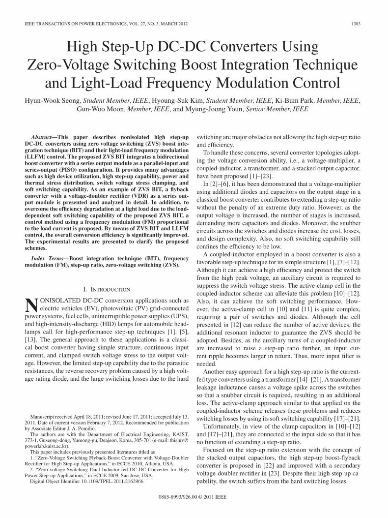
Fig. 11. Minimum FM ratio and maximum modulated frequency for ZVS of Q1 at light load: (a) Minimum FM ratio k. (b) Maximum modulated frequencyf ′S .
a resonant period ωr , the time interval Δt0 can be derived as
Δt0 =π
2n√
Llkg (Cj1 + Cj2). (27)
Thus, the magnitude of ΔIlkg0 can be expressed by using (11)and (27) as follows:
ΔIlkg0 =nVI + VC O2 − VC b√
Llkg/(Cj1 + Cj2). (28)
It is pointed out that the load current information is nowhere in(26)–(28). That is, each value is constant regardless of the loadlevel. Therefore, the current waveforms are distorted due to thereduced powering current compared with these constant valuesat a light load.
B. Effect of Decreasing Switching Frequency at Light Load
By decreasing a switching frequency for the load range belowIO min ZVS Lkg , Q1 can recover ZVS by the energy stored in amagnetizing inductor Lm .
Fig. 10 shows the effect of decreasing a switching frequencyat a light load. Compared with the waveforms before the fre-quency modulation (FM) shown in Fig. 9(b), ΔIlkg0 and Δt0are not changed and the switching period and the magnetiz-ing current ripple are extended to T ′
S and ΔI ′Lm , respectively,until the minimum value of I ′Lm , I ′Lm min , becomes nega-tive. This negative magnetizing current can provide ZVS ofQ1 even at a light load. Meanwhile, since the increased valueof the maximum magnetizing current I ′Lm max still providesZVS of Q2 , ZVS of all switches is obtained by decreasing aswitching frequency. It is also noted that the shaded areas inboth Figs. 9(b) and 10 are the same and this value is identicalto nIO .
To obtain a general condition satisfying ZVS of Q1 below theload condition of IO min ZVS Lkg , a FM ratio k can be defined as
k =fS
f ′S
=T ′
S
TS=
ΔI ′Lm
ΔILm> 1 (29)
where the prime mark implies the parameters after FM. Sincethe negative value of I ′Lm min discharges a junction capacitor ofQ1 and charges that of Q2 in a short time during Δt0 , the ZVS
conditions of Q1 by FM can be obtained as follows:
I ′Lm min = Iin − 12ΔI ′Lm = MIO − 1
2ΔI ′Lm < 0 (30)
12Lm I
′2Lm min ≥ 1
2(COSS1 + COSS2)V 2
C O1 . (31)
By substituting (30) into (31), a minimum FM ratio accordingto the load current can be derived as
k ≥ 2M
ΔILmIO + 2
√COSS1 + COSS2
Lm· VC O1
ΔILm. (32)
Equation (32) can also be expressed in terms of the frequencyrelation as
f ′S ≤
fS
(2M/ΔILm )IO + 2√
(CO S S 1 + CO S S 2 )/Lm · (VC O 1/ΔILm ).
(33)
Fig. 11 depicts a minimum FM ratio and a maximum modulatedfrequency for achieving ZVS of Q1 according to the load con-dition. A solid-line in Fig. 11(a) shows the critical value of k toachieve the soft switching of Q1 assuming that Lm is designedto satisfy the boundary conduction mode (BCM) at a 10% load.Under this assumption, to achieve ZVS below a 20% load con-dition, k should be higher than k = 4.3. In addition, since thevalue of Lm influences both the magnitude of ΔILm and thevalue of the load current satisfying BCM, the FM ratio can beadjusted by Lm as depicted by dotted lines in Fig. 11(a). Thesephenomena also appear with respect to the frequency relationas shown in Fig. 11(b) when fS is 70 kHz. It is noted that a fre-quency less than 70/4.3 ≈ 16.3 kHz can guarantee ZVS belowa 20% load condition when Lm is designed to satisfy BCM at a10% load.
C. Control Strategy
Prior to confirming a frequency modulation ratio k accord-ing to the load condition, ZVS load boundary IO min ZVS Lkgshould be selected first by using (25). At the load range aboveIO min ZVS Lkg , since all switches can be turned on under ZVS

SEONG et al.: HIGH STEP-UP DC-DC CONVERTERS USING ZERO-VOLTAGE SWITCHING BOOST 1391
Fig. 12. FM control strategies according to load condition whenfS = 70 kHz.
conditions due to the sufficient energy stored in the leakage in-ductor, the FM control is unnecessary. Nevertheless, if the FMcontrol is applied to the system, larger conduction losses causedby the increased ΔILm occur. Thus, a fixed high-frequencycontrol is recommended in this load range.
At the load range below IO min ZVS Lkg , the FM control canbe effective to improve the conversion efficiency through therecovered ZVS. From Fig. 11(b), since the region at below thecurves allows ZVS of Q1 , a constant modulated-frequencyf ′
S iseligible below the desired load current. This desired load currentis defined as a ZVS load boundary by FM, IO max ZVS FM . Itcan be derived from (32) as follows:
IO m ax ZVS FM =1M
(ΔILm
2· k −
√CO S S 1 + CO S S 2
Lm
· VC O 1
)
.
(34)If IO max ZVS FM is located at a 20% load, a constant frequencyless than 16.3 kHz can ensure ZVS of all switches at the loadrange below IO max ZVS FM from Fig. 11(b).
In summary, Fig. 12 shows control strategies according tothe load condition when fS = 70 kHz. It is assumed that theZVS load boundary by Llkg , IO min ZVS Lkg , is set at a 40% loadand the ZVS load boundary by FM, IO max ZVS FM , is set ata 20% load, respectively. Between these two boundaries, thereis a frequency modulating region to avoid the abrupt frequencytransition fromfS to f ′
S .For an easy implementation, the slope of this region is
assumed to be linear. If an FM ratio is increased untilIO max ZVS FM reaches IO min ZVS Lkg , i.e., IO max ZVS FM =IO min ZVS Lkg , the abrupt frequency transition as well as highconduction losses caused by the excessive FM ratio nearIO max ZVS FM can occur even though it provides the ZVS at anentire load range. Thus, a comparison between reduced switch-ing losses and increased conduction losses due to FM should beconsidered when selecting IO max ZVS FM .
D. Comparison With Other Methods Extending ZVS Range
To improve the efficiency, focused on reducing the switchinglosses, several methods are proposed [31]–[39]. These tech-niques can be classified into two categories: the quasiresonanttechnique [31], [32] and the active-clamp technique [33]–[39].
In the quasiresonant technique, the constant off-time con-trol method at boundary conduction mode (BCM) can reducethe switching losses by using a resonant valley [31]. Theoreti-cally, since the switching frequency approaches infinity as theload current approaches zero, this converter suffers from an ex-tremely wide frequency range and excessive switching lossesat a light load. To handle this problem, adaptive off-time con-trol has been proposed, which increases the off-time adaptivelywhile maintaining the soft switching at a light load [32]. How-ever, the quasiresonant technique usually operates the converterin BCM and discontinuous conduction mode (DCM) at an en-tire load range. It causes high conduction losses at a heavy load.This is the main limitation of the quasiresonant technique.
The active-clamp technique can not only reduce the conduc-tion losses by operating in continuous conduction mode (CCM)but also achieve the soft switching for both switches by uti-lizing the energy stored in a leakage inductor. Based on theactive-clamp circuit presented in [33], several modified circuitshave been proposed [34]–[38]. Although they have good perfor-mance in efficiency at heavy load condition, the load-dependentZVS condition of the main switch and constant frequencycontrol result in poor efficiency at light load condition due tothe high switching losses.
To achieve the ZVS of the main switch at any load condi-tions, a variable frequency control by adjusting the off-timewith noncomplementary gate signals has been proposed [39].Since an auxiliary switch is turned ON for a short time beforethe main switch is turned ON, the recycled leakage energy canbe used to achieve the ZVS of the main switch, which reducesthe circulating energy effectively compared to the conventionalcomplementary switching techniques. However, the ZVS of anauxiliary switch is lost at an entire load range due to the noncom-plementary gate signals. Furthermore, there is a narrow currentpulse in the secondary side when the auxiliary switch turns ON,which can degrade the EMI performance.
The proposed LLFM technique uses a variable frequency con-trol with complementary gate signals. The main difference fromthe previously introduced scheme is that there are two constantfrequency ranges according to the load level. Also, there is a fre-quency transition range between two constant frequency rangesas noted in Fig. 12. Especially, the lower constant frequencycan determine the ZVS recovering load range. Therefore, com-pared with [33]–[38], the proposed method can achieve ZVSeven at a light load while maintaining the same soft switchingperformance and the same device stresses at heavy load condi-tion. Compared with [39], the auxiliary switch can also achieveZVS without any narrow current pulse in the secondary side.However, the circulating current is higher.
Table I summarizes the comparison of the several techniquesto extend the ZVS load range. Q1 and Q2 in Table I indicate amain switch and an auxiliary switch, respectively.
1392 IEEE TRANSACTIONS ON POWER ELECTRONICS, VOL. 27, NO. 3, MARCH 2012
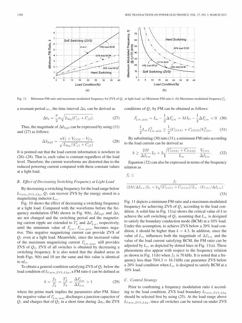
TABLE ICOMPARISON OF SEVERAL ZVS RANGE EXTENSION TECHNIQUES
Fig. 13. Topology variations: (a) Isolated sepic converter as a series outputmodule. (b) Current-fed half-bridge (CFHB) converter as a series output module.
V. TOPOLOGY VARIATIONS
With the proposed ZVS BIT, other types of current-fed con-verter as a series output module are presented briefly. The pro-posed ZVS BIT concept can be applied to any current-fed typeconverters. However, to increase the device utilization and mini-mize the number of active and passive components, the commonparts integration presented in Section II-A should be considered.Under this rule, an isolated sepic converter and a current-fed
Fig. 14. Estimated loss comparison at 20% load condition.
half-bridge (CFHB) converter as a series output module are pro-posed, as shown in Fig. 13. These converters are also suitablecandidates for the high step-up applications.
The pulsating input current of the ZVS flyback-boost con-verter with VDR is relatively high, which can cause a high con-duction loss on the switches. It is one of the main limitations,which results from the inherent characteristics of both a flybackconverter and a VDR. Therefore, the use in low-to-mediumpower applications is recommended. If the high pulsating in-put current is troublesome, the isolated sepic converter shownin Fig. 13(a) can be an alternative because a boost inductor Lb
relieves it. The reduced current stresses on the switches can alsoreduce the conduction losses.
To diminish the pulsating input current further, the CFHBconverter shown in Fig. 13(b) is more attractive. Its interleavinggate signals with two boost inductors, L1 and L2 , provide theripple cancellation between two phases. Also, the half-reducedinductor currents can reduce the conduction losses in the boost

SEONG et al.: HIGH STEP-UP DC-DC CONVERTERS USING ZERO-VOLTAGE SWITCHING BOOST 1393
TABLE IICHARACTERISTICS OF THE PROPOSED CONVERTERS

1394 IEEE TRANSACTIONS ON POWER ELECTRONICS, VOL. 27, NO. 3, MARCH 2012
TABLE IIIDESIGN SPECIFICATIONS AND CIRCUIT PARAMETERS
inductor windings. Therefore, it can be adapted to high powerapplications.
A series output module can be properly selected for the de-sired applications by considering the input current ripple, ratedpower level, device stresses, number of components, step-up ra-tio, and so on. To increase a step-up ratio further, secondaryrectifiers can be modified to a voltage-doubler rectifier asadopted in the ZVS flyback-boost converter with a VDR.
All of these converters have the common features of ZVSBIT. The output voltage is stacked as (1). Each average value oftwo powering currents satisfies (2) and (3). The switch voltagestresses are clamped to VC O 1 . The leakage inductor alleviatesthe reverse recovery problem of the secondary rectifiers. A mainswitch has a load-dependent ZVS condition, whereas an auxil-iary switch has a wide ZVS load range. Thus, the LLFM controlmethod can be also applied to these converters.
Despite the many advantages, the integrated boost converterlimits the use of the proposed converters only to applicationswhere no isolation is required.
Table II summarizes the characteristics of these proposedconverters.
VI. EXPERIMENTAL VERIFICATION
A. Design Example
To verify the validity of the proposed converters employingthe ZVS BIT and LLFM control, a prototype of 250 W ZVSflyback-boost converter with VDR is implemented. The designspecifications and circuit parameters are given in Table III.
From the input and output voltage specifications, M can becalculated as M = 9.52. By using (14), a nominal duty ratio Dand a transformer turns ratio n can be selected by considering
the conversion efficiency, i.e., D is about 0.6 and n = 3.5. Then,select Lm that satisfies the boundary conduction mode (BCM)at a desired load condition and measure the leakage inductor,i.e., Lm = 280 μH for a 10% load BCM and the intrinsic Llkg =1.5 μH. To extend a ZVS load range by a leakage inductor,an external inductor is added by using (20) and Fig. 7, i.e.,total Llkg = 10 μH to ensure ZVS above a 25% load condition.Since the increased Llkg decreases the step-up ratio due to thedamping effect of Q in (12), the nominal duty ratio D shouldbe confirmed by using (12) and Fig. 6(b), i.e., D = 0.63. Withthe selected n and D, VC O 1 and VC O 2 are designed to be about110 V and 290 V, respectively. Thus, the switches and diodescan be selected by considering the voltage and current stressesshown in Table III. The capacitors Cb , CO 1 , and CO 2 , whichsatisfy the desired voltage ripple conditions, can also be selectedby using (17)–(19).
To apply the LLFM control to this converter, the ZVS loadboundary by a leakage inductor, IO min ZVS Lkg , should be de-fined. With the value of Llkg , IO min ZVS Lkg is located arounda 25% load condition derived from (25) and Fig. 7. However,since (25) does not consider the effect of parasitic capacitors ofa transformer, the actual ZVS load boundary by Llkg is higherthan the theoretical value. Therefore, IO min ZVS Lkg is set ata 40% load condition, which can be confirmed clearly by theexperiments. Next, to define the ZVS load boundary by FM,IO max ZVS FM , a loss comparison between without and withthe LLFM is preceded. Fig. 14 shows the results at a 20% loadcondition. Although the proposed LLFM control has higherconduction losses due to increased currents, much less switch-ing losses due to ZVS turn-on can contribute the efficiencyimprovement. Thus, IO max ZVS FM is set at a 22% load con-dition, resulting in k = 4.67 and f ′
S = 15 kHz from (34) and

SEONG et al.: HIGH STEP-UP DC-DC CONVERTERS USING ZERO-VOLTAGE SWITCHING BOOST 1395
Fig. 15. Digital implementation of LLFM control: (a) Schematic. (b) Controlalgorism.
Fig. 11. To accommodate an easy implementation, the linearfrequency modulating region exists between 22% and 40% loadconditions.
In summary, IO min ZVS Lkg = 0.4IO max , IO max ZVS FM =0.22IO max , k = 4.67, and f ′
S = 15 kHz. Thus, all switchesemployed in the converter can achieve ZVS both above 40% loadcondition by a leakage inductor and below 22% load conditionthrough the LLFM control. This design example mainly focuseson the verification of the ZVS recovering capability through theLLFM control. The ZVS of an entire load range can be realizedby increasing either a leakage inductor or a FM ratio slightly.
B. Digital Implementation of LLFM Control
The overall system has been implemented fully in soft-ware using a microcontroller unit (MCU), Texas InstrumentTMS320F28027, as shown in Fig. 15(a). The voltage and cur-rent sensing signals, VO [k] and IO [k], have been measured with
Fig. 16. Key experimental waveforms at a full load: (a) Primary leakagecurrent and secondary link capacitor current. (b) Current and voltage waveformsof the switches. (c) Current and voltage waveforms of the output rectifiers.
the 12-bit A/D converter. The switching frequency can be mod-ulated with a counter unit in the MCU so that the updated fre-quency fS [k] is generated from the current sensing signal IO [k].This control algorism for FM is shown in Fig. 15(b). When IO [k]is higher than IO min ZVS Lkg , the switching frequencyfS [k]becomes fS . On the other hand, when IO [k] is lower thanIO max ZVS FM , the switching frequencyfS [k] becomes f ′
S . Be-tween these two load boundaries, the frequency modulation isperformed linearly according to IO [k] as
fS [k] =fS − f ′
S
IO max ZVS lkg − IO min ZVS FMIO [k] + f ′
S . (35)
After finishing the FM control, the voltage-mode controller uti-lizing a PI-control law executes the output voltage to regulate

1396 IEEE TRANSACTIONS ON POWER ELECTRONICS, VOL. 27, NO. 3, MARCH 2012
Fig. 17. ZVS waveforms of switches: (a) Q1 at full load. (b) Q2 at full load. (c) Q1 at half load. (d) Q2 at half load.
Fig. 18. Key experimental waveforms without LLFM control at a 15% load:(a) Primary leakage current and secondary link capacitor current. (b) Currentand voltage waveforms of the switches.
cycle by cycle, since the sampling frequency is synchronizedwith the updated frequency.
C. Experimental Results
Fig. 16 indicates the key experimental waveforms of theprototype converter at the full load condition, which are wellcoincided with aforementioned theoretical analysis. Fig. 16(a)
Fig. 19. Key experimental waveforms with LLFM control at a 15% load:(a) Primary leakage current and secondary link capacitor current. (b) Currentand voltage waveforms of the switches.
shows the primary leakage current and secondary link capaci-tor current. Fig. 16(b) shows current and voltage waveforms ofthe switches. The negative currents of the switches by the aid ofZVS BIT offer ZVS of all switches. Fig. 16(c) shows the currentand voltage waveforms of the output rectifiers. The alleviateddi/dt of IDO 1(t) and IDO 2(t) offers the current snubbing effectand reduces the reverse recovery problem. From Fig. 16(b) and(c), the voltages across the switches and output rectifiers arewell clamped to VC O 1 and VC O 2 , respectively.

SEONG et al.: HIGH STEP-UP DC-DC CONVERTERS USING ZERO-VOLTAGE SWITCHING BOOST 1397
Fig. 20. ZVS waveforms of main switch Q1 according to load conditions: (a) without LLFM control and (b) with LLFM control.
Fig. 17 shows that the switches Q1 and Q2 are turned onafter VQ 1 and VQ 2 drop to 0 V, i.e., ZVS of all switches isachieved. Theoretically, with the values of the leakage inductorand junction capacitors of the switches used in the experiment,ZVS of all switches should be guaranteed approximately from25% to 100% load conditions as noted in Fig. 7. However, inreal systems, parasitic capacitors of a transformer make the ZVSrange narrow so that it is guaranteed approximately from 40%to 100% load conditions.
Fig. 18 shows the key experimental waveforms of the pro-posed converter without LLFM control at a 15% load condition.It agrees well with Fig. 9(b) except for the distortion of thecurrent waveforms due to the hard switching noise. It is notedthat the magnitude of the abrupt build-up current ΔIlkg0 is about1.2 A, which is well matched with the estimated value, i.e., 1.3 A,from (28). This build-up current affects the shape of Ilkg (t) dom-
inantly at light load condition. Furthermore, the main switch Q1suffers from the hard switching so that the considerable high-frequency switching noises are observed when it turns ON. Onthe contrary, the auxiliary switch Q2 still maintains ZVS due tothe sufficient energy stored in Lm .
In case of applying the LLFM control, the current waveformsare changed, as shown in Fig. 19, which are well coincidedwith Fig. 10. Since the modulated frequency below a 22% loadcondition is 15 kHz, the magnetizing current ripple ΔILm isextended accordingly. It is worth noticing that the negative valueof Ilkg (t) due to the extended ΔILm offers ZVS of the mainswitch Q1 . Therefore, no switching noise occurs unlike Fig. 18.Furthermore, the auxiliary switch Q2 also achieves ZVS.
Fig. 20 shows the ZVS waveforms at light load conditionswith and without the LLFM control. Without LLFM control,ZVS of Q1 is lost from a 40% load condition due to the
1398 IEEE TRANSACTIONS ON POWER ELECTRONICS, VOL. 27, NO. 3, MARCH 2012
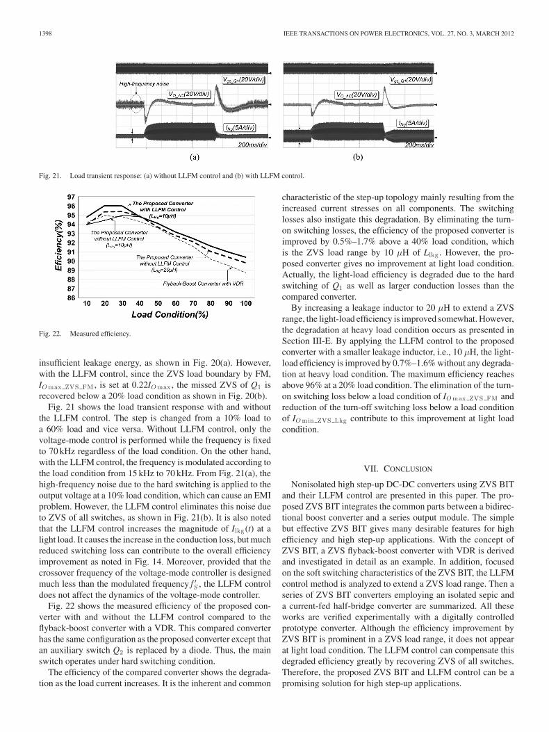
Fig. 21. Load transient response: (a) without LLFM control and (b) with LLFM control.
Fig. 22. Measured efficiency.
insufficient leakage energy, as shown in Fig. 20(a). However,with the LLFM control, since the ZVS load boundary by FM,IO max ZVS FM , is set at 0.22IO max , the missed ZVS of Q1 isrecovered below a 20% load condition as shown in Fig. 20(b).
Fig. 21 shows the load transient response with and withoutthe LLFM control. The step is changed from a 10% load toa 60% load and vice versa. Without LLFM control, only thevoltage-mode control is performed while the frequency is fixedto 70 kHz regardless of the load condition. On the other hand,with the LLFM control, the frequency is modulated according tothe load condition from 15 kHz to 70 kHz. From Fig. 21(a), thehigh-frequency noise due to the hard switching is applied to theoutput voltage at a 10% load condition, which can cause an EMIproblem. However, the LLFM control eliminates this noise dueto ZVS of all switches, as shown in Fig. 21(b). It is also notedthat the LLFM control increases the magnitude of Ilkg (t) at alight load. It causes the increase in the conduction loss, but muchreduced switching loss can contribute to the overall efficiencyimprovement as noted in Fig. 14. Moreover, provided that thecrossover frequency of the voltage-mode controller is designedmuch less than the modulated frequencyf ′
S , the LLFM controldoes not affect the dynamics of the voltage-mode controller.
Fig. 22 shows the measured efficiency of the proposed con-verter with and without the LLFM control compared to theflyback-boost converter with a VDR. This compared converterhas the same configuration as the proposed converter except thatan auxiliary switch Q2 is replaced by a diode. Thus, the mainswitch operates under hard switching condition.
The efficiency of the compared converter shows the degrada-tion as the load current increases. It is the inherent and common
characteristic of the step-up topology mainly resulting from theincreased current stresses on all components. The switchinglosses also instigate this degradation. By eliminating the turn-on switching losses, the efficiency of the proposed converter isimproved by 0.5%–1.7% above a 40% load condition, whichis the ZVS load range by 10 μH of Llkg . However, the pro-posed converter gives no improvement at light load condition.Actually, the light-load efficiency is degraded due to the hardswitching of Q1 as well as larger conduction losses than thecompared converter.
By increasing a leakage inductor to 20 μH to extend a ZVSrange, the light-load efficiency is improved somewhat. However,the degradation at heavy load condition occurs as presented inSection III-E. By applying the LLFM control to the proposedconverter with a smaller leakage inductor, i.e., 10 μH, the light-load efficiency is improved by 0.7%–1.6% without any degrada-tion at heavy load condition. The maximum efficiency reachesabove 96% at a 20% load condition. The elimination of the turn-on switching loss below a load condition of IO max ZVS FM andreduction of the turn-off switching loss below a load conditionof IO min ZVS Lkg contribute to this improvement at light loadcondition.
VII. CONCLUSION
Nonisolated high step-up DC-DC converters using ZVS BITand their LLFM control are presented in this paper. The pro-posed ZVS BIT integrates the common parts between a bidirec-tional boost converter and a series output module. The simplebut effective ZVS BIT gives many desirable features for highefficiency and high step-up applications. With the concept ofZVS BIT, a ZVS flyback-boost converter with VDR is derivedand investigated in detail as an example. In addition, focusedon the soft switching characteristics of the ZVS BIT, the LLFMcontrol method is analyzed to extend a ZVS load range. Then aseries of ZVS BIT converters employing an isolated sepic anda current-fed half-bridge converter are summarized. All theseworks are verified experimentally with a digitally controlledprototype converter. Although the efficiency improvement byZVS BIT is prominent in a ZVS load range, it does not appearat light load condition. The LLFM control can compensate thisdegraded efficiency greatly by recovering ZVS of all switches.Therefore, the proposed ZVS BIT and LLFM control can be apromising solution for high step-up applications.

SEONG et al.: HIGH STEP-UP DC-DC CONVERTERS USING ZERO-VOLTAGE SWITCHING BOOST 1399
In summary, this paper summarizes the general law and struc-ture of the ZVS BIT. Also, the LLFM control method is expectedto be well suited for ZVS BIT as well as various active-clampcircuit employed converters.
REFERENCES
[1] Q. Zhao and F. C. Lee, “High-efficiency, high step-up DC-DC converters,”IEEE Trans. Power Electron., vol. 18, no. 1, pp. 65–73, Jan. 2003.
[2] M. Prudente, L. L. Pfitscher, G. Emmendoerfer, E. F. Romaneli, andR. Gules, “Voltage multiplier cells applied to non-isolated DC-DC con-verters,” IEEE Trans. Power Electron., vol. 23, no. 2, pp. 871–887, Mar.2008.
[3] J. A. Starzyk, Y.-W. Jan, and F. Qiu, “A DC-DC charge pump designbased on voltage doubler,” IEEE Trans. Circuit Syst. I, vol. 48, no. 3,pp. 350–359, Mar. 2001.
[4] H. Ye and F. L. Luo, “Positive output super-lift converters,” IEEE Trans.Power Electron., vol. 18, no. 1, pp. 105–113, Jan. 2003.
[5] E. H. Ismail, M. A. Al-Saffar, A. J. Sabzali, and A. A. Fardoun, “A familyof single-switch PWM converters with high step-up conversion ratio,”IEEE Trans. Circuit Syst. I, vol. 55, no. 4, pp. 1159–1171, May 2008.
[6] R. D. Middlebrook, “Transformerless DC-to-DC converters with largeconversion ratios,” IEEE Trans. Power Electron., vol. 3, no. 4, pp. 484–488, Oct. 1988.
[7] D. A. Grant, Y. Darroman, and J. Suter, “Synthesis of tapped-inductorswitched-mode converters,” IEEE Trans. Power Electron., vol. 22, no. 6,pp. 1271–1279, Nov. 2005.
[8] R. J. Wai and R. Y. Duan, “High step-up converter with coupled inductor,”IEEE Trans. Power Electron., vol. 20, no. 5, pp. 1025–1035, Sep. 2005.
[9] E. J. Copple and A. Heights, “High efficiency DC step-up voltage con-verter,” US Patent 5929614, Jul. 1999.
[10] R. J. Wai, C. Y. Lin, and C. C. Chu, “High step-Up DC-DC converter forfuel cell generation system,” in Proc. IEEE IECON, Nov. 2004, pp. 57–62.
[11] R. J. Wai and C. Y. Lin, “High-efficiency, high step-up DC-DC converterfor fuel cell generation system,” in Proc. Inst. Elect. Eng.—Elect. PowerAppl., Sep. 2005, vol. 152, no. 5, pp. 1371–1378.
[12] T.-F. Wu, Y.-S. Lai, J.-C. Hung, and Y.-M. Chen, “Boost converter withcoupled inductors and buck-boost type of active clamp,” IEEE Trans. Ind.Electron., vol. 55, no. 1, pp. 154–162, Jan. 2008.
[13] W. Li and X. He, “Review of nonisolated high-step-up DC/DC convertersin photovoltaic grid-connected applications,” IEEE Trans. Ind. Electron.,vol. 58, no. 4, pp. 1239–1250, Apr. 2011.
[14] P. J. Wolfs, “A current sources DC-DC converter derived via the dualityprinciple from half-bridge converter,” IEEE Trans. Ind. Electron., vol. 40,no. 1, pp. 139–144, Feb. 1993.
[15] R. Redl and N. O. Sokal, “Push-pull current-fed multiple-output DC/DCpower converter with only one inductor and with 0 to 100% switch dutyratio,” in Proc. IEEE PESC, 1980, pp. 341–345.
[16] De Aragao Filho, W. C. P., and I. Barbi, “A comparison between twocurrent-fed push-pull DC-DC converters—Analysis, design and experi-mentation,” in Proc. INTELEC, 1996, pp. 313–320.
[17] S.-K. Han, H.-K. Yoon, G.-W. Moon, M.-J. Youn, Y.-H. Kim, andK.-H. Lee, “A new active clamping zero-voltage switching PWM current-fed half-bridge converter,” IEEE Trans. Power Electron., vol. 20, no. 6,pp. 1271–1279, Nov. 2005.
[18] H. Xiao and S. Xie, “A ZVS bidirectional DC-DC converter with phase-shift plus PWM control scheme,” IEEE Trans. Power Electron., vol. 23,no. 2, pp. 813–823, Mar. 2008.
[19] E. Adib and H. Farzanehfard, “Zero-voltage transition current-fed full-bridge PWM converter,” IEEE Trans. Power Electron., vol. 24, no. 4,pp. 1041–1047, Apr. 2009.
[20] J.-M. Kwon and B.-H. Kwon, “High step-up active-clamp converter withinput-current doubler and output-voltage doubler for fuel cell power sys-tems,” IEEE Trans. Power Electron., vol. 24, no. 1, pp. 108–115, Jan.2009.
[21] R. Watson and F. C. Lee, “A soft-switched full-bridge boost converteremploying an active clamp circuit,” in Proc. IEEE PESC, 1996, pp. 1948–1954.
[22] T. J. Liang and K. C. Tseng, “Analysis of integrated boost-flyback step-up converter,” in Proc. Inst. Elect. Eng.—Elect. Power Appl., Mar. 2005,vol. 152, no. 2, pp. 217–225.
[23] J. W. Baek, M. H. Ryoo, T. J. Kim, D. W. Yoo, and J. S. Kim, “High boostconverter using voltage multiplier,” in Proc. IEEE IECON, Nov. 2005,pp. 567–572.
[24] H.-S. Park, C.-E. Kim, G.-W. Moon, and J.-C. Lim, “Novel current-stressreduction technique for boost integrated half-bridge DC/DC converterwith voltage doubler type rectifier,” in Proc. IEEE PESC, Jun. 2006,pp. 1–6.
[25] T. J. Liang and K. C. Tseng, “Analysis of integrated boost-flyback step-upconverter,” in IEE Proc. Electric Power Appl., Mar. 2005, vol. 152, no. 2,pp. 217–225.
[26] T. Dumrongkittigule, V. Tarateeraseth, and W. Khan-ngern, “A new in-tegrated inductor with balanced switching technique for common modeEMI reduction in high step-up DC/DC converter,” in Proc. 17th Int. ZurichSymp. Electromagn. Compat., Feb. 2006, pp. 541–544.
[27] W. Li, Y. Zhao, Y. Deng, and X. He, “Interleaved converter with voltagemultiplier cell for high step-up and high efficiency conversion,” IEEETrans. Power Electron., vol. 25, no. 9, pp. 2397–2408, Sep. 2010.
[28] K.-B. Park, G.-W. Moon, and M.-J. Youn, “Nonisolated high step-up boostconverter integrated with sepic converter,” IEEE Trans. Power Electron.,vol. 25, no. 9, pp. 2266–2275, Sep. 2010.
[29] S.-K. Han, H.-K. Yoon, G.-W. Moon, M.-J. Youn, Y.-H. Kim, andK.-H. Lee, “A new active clamping zero-voltage switching PWM current-fed half-bridge converter,” IEEE Trans. Power Electron., vol. 20, no. 6,pp. 1271–1279, Nov. 2005.
[30] W. Li and X. He, “A family of interleaved DC-DC converters deducedfrom a basic cell with winding-cross-coupled inductors (WCCIs) for highstep-up or step-down conversions,” IEEE Trans. Power Electron., vol. 23,no. 4, pp. 1791–1801, Jul. 2008.
[31] J. B. Lio, M. S. Lin, D. Y. Chen, and W. S. Feng, “Single -switch,soft-switching flyback converter,” IEE Electron. Lett., vol. 32, no. 16,pp. 1429–1430, Jun. 1996.
[32] Y. Panov and M. M. Jovanovic, “Adaptive off-time control for variable-frequency, soft-switched flyback converter at light loads,” IEEE Trans.Power Electron., vol. 17, no. 4, pp. 596–603, Jul. 2002.
[33] R. Watson, F. C. Lee, and G. C. Hua, “Utilization of an active-clampcircuit to achieve soft switching in flyback converters,” IEEE Trans.Power Electron., vol. 11, no. 1, pp. 162–169, Jan. 1996.
[34] Y.-K. Lo and J.-Y. Lin, “Active-clamping ZVS flyback converter em-ploying two transformers,” IEEE Trans. Power Electron., vol. 22, no. 6,pp. 2416–2423, Nov. 2007.
[35] Y.-K. Lo, T.-S. Kao, and J.-Y. Lin, “Analysis and design of an interleavedactive-clamping forward converter,” IEEE Trans. Ind. Electron., vol. 54,no. 4, pp. 2323–2332, Aug. 2007.
[36] L. Huber and M. M. Jovanovic, “Forward-flyback converter with currentdoubler rectifier: Analysis, design, and evaluation results,” IEEE Trans.Power Electron., vol. 14, no. 1, pp. 184–192, Jan. 1999.
[37] C. T. Choi, C. K. Li, and S. K. Kok, “Control of an active clamp discontin-uous conduction mode flyback converter,” in Proc. IEEE Power Electron.Drive Syst. Conf., 1999, vol. 2, pp. 1120–1123.
[38] G.-B. Koo and M. J. Youn, “A new zero-voltage switching active clampflyback converter,” in Proc. IEEE Power Electron. Spec. Conf., Jun. 2004,pp. 508–510.
[39] J. Zhang, X. Huang, X. Wu, and Z. Qian, “A high efficiency flybackconverter with new active clamp technique,” IEEE Trans. Power Electron.,vol. 25, no. 7, pp. 1775–1785, Jul. 2010.
Hyun-Wook Seong (S’08) was born in Korea, in1981. He received the B.S. degree in electronics en-gineering from Ajou University, Suwon, in 2006, andthe M.S. degree in Graduate School of AutomotiveTechnology at the Korea Advanced Institute of Sci-ence and Technology (KAIST), Daejeon, in 2008. Heis currently working toward the Ph.D degree in elec-trical engineering at KAIST.
His current research interests include power con-verters, digital power control, converter modeling,and server power system.

1400 IEEE TRANSACTIONS ON POWER ELECTRONICS, VOL. 27, NO. 3, MARCH 2012
Hyoung-Suk Kim (S’09) was born in Korea, in 1981.He received the B.S. degree in electronics engineer-ing from Pusan National University, Pusan, in 2007.He is currently working toward the Ph.D degree inelectrical engineering at the Korea Advanced Insti-tute of Science and Technology (KAIST), Daejeon.
His current research interests include DC-DCpower converters, digital controller design, LEDcolor control, and battery equalizers.
Ki-Bum Park (S’07–M’10) was born in Korea, in1981. He received the B.S., M.S., and Ph.D. degreesin electrical engineering from the Korea AdvancedInstitute of Science and Technology (KAIST), Dae-jeon, in 2003, 2005, and 2010, respectively.
He is currently a Scientist at ABB CorporateResearch Center, Baden-Dattwil, Switzerland. Hisresearch interests include power converters, serverpower system, high power density adapter, batterymanagement system, and display driver circuit.
Dr. Park received the 2nd Prize Paper award fromthe International Telecommunications Energy Conference (INTELEC), in 2009.
Gun-Woo Moon (S’92–M’00) received the M.S.and Ph.D. degrees in electrical engineering from theKorea Advanced Institute of Science and Technology(KAIST), Daejeon, in 1992 and 1996, respectively.
He is currently a Professor in the Department ofElectrical Engineering, KAIST. His research inter-ests include modeling, design and control of powerconverters, soft-switching power converters, resonantinverters, distributed power systems, power-factorcorrection, electric drive systems, driver circuits ofplasma display panels, and flexible AC transmission
systems.Dr. Moon is a member of the Korean Institute of Power Electronics (KIPE),
Korean Institute of Electrical Engineers (KIEE), Korea Institute of Telematicsand Electronics (KITE), Korea Institute of Illumination Electronics and Indus-trial Equipment (KIIEIE), and Society for Information Display (SID).
Myung-Joong Youn (S’74–M’78–SM’98) was bornin Seoul, Korea, in 1946. He received the B.S. degreein electrical engineering from Seoul National Univer-sity, Seoul, in 1970, and the M.S. and Ph.D. degreesin electrical engineering from the University of Mis-souri, Columbia, in 1974 and 1978, respectively.
In 1978, he joined the Air-Craft Equipment Divi-sion, General Electric Company, Erie, PA, where hewas an Individual Contributor on Aerospace Electri-cal System Engineering. Since 1983, he has been aProfessor at the Korea Advanced Institute of Science
and Technology (KAIST), Daejeon. His research activities are in the areas ofpower electronics and control, which include the drive systems, rotating elec-trical machine design, and high-performance switching regulators.
Dr. Youn is a member of the Institution of Electrical Engineers, U.K., theKorean Institute of Power Electronics (KIPE), the Korean Institute of Electri-cal Engineers (KIEE), and the Korea Institute of Telematics and Electronics(KITE).