ieee transactions on aerospace and electronic systems …rabie-ben-atitallah.com/paper/taes.pdf ·...
TRANSCRIPT

0018-9251 (c) 2017 IEEE. Personal use is permitted, but republication/redistribution requires IEEE permission. See http://www.ieee.org/publications_standards/publications/rights/index.html for more information.
This article has been accepted for publication in a future issue of this journal, but has not been fully edited. Content may change prior to final publication. Citation information: DOI 10.1109/TAES.2017.2733858, IEEETransactions on Aerospace and Electronic Systems
IEEE TRANSACTIONS ON AEROSPACE AND ELECTRONIC SYSTEMS 1
FPGA-Centric Design Process for AvionicSimulation and Test
Rabie Ben Atitallah, Venkatasubramanian Viswanathan, Nicolas Belanger, Jean-Luc Dekeyser
F
Abstract—Real-time computing systems are increasingly used inaerospace and avionic industries. In the face of power challenge,performance requirements and demands for higher flexibility, hardwaredesigners are directed towards reconfigurable computing using FPGAs(Field Programmable Gate Arrays) that offer high computation rates perwatt and adaptability to the application constraints. However, consider-ing reconfigurable computing in the avionic design process leads to sev-eral challenges for system developers. Indeed, such technology shouldbe validated along the Verification & Validation (V&V) cycle starting withsimulation tools, passing through the test benches and finishing withthe integration phase. For each step the FPGA can play an essentialrole to achieve better performances, more adaptive systems and cost-effective solutions. In this paper, we present a seamless FPGA-centricdesign process for avionic equipments. Along this process, we redefinethe role of the FPGA circuits to cover the simulation, the test and theintegration steps. First, reconfigurable logics are used in the frame ofheterogeneous CPU/FPGA computing in order to obtain high speed-up for real-time avionic simulation. The proposed environment supportsdynamic execution model enabling reconfiguration during runtime toavoid the timing constraint violation. Second, the FPGA is used as a keysolution to offer versatile test benches and to converge toward unifiedtest and simulation tools. We have designed several commercial InputOutput (I/O) Intellectual Property (IP) systems with dynamic runtime re-configuration capabilities, in order to mitigate component obsolescenceand to provide increased flexibility and decreased design time. Third atthe integration phase, we use the conventional tools to make profit fromreconfigurable technology in embedded avionic applications in order todeliver high computation rates and to adapt their functioning mode toprovide reliability, fault tolerance, deterministic timing guarantees, andenergy efficiency.
Index Terms—Avionic systems, Verification & Validation, Design pro-cess, FPGA, Reconfigurable computing, Simulation, Test, I/O IP, Dy-namic reconfiguration.
1 INTRODUCTION
Continuously growing aerospace industry competitive-ness pushes avionic actors to revisit and strengthen theirmethodology and tools of the Verification & Validation(V&V) design cycle. In this perspective, the technicalareas of simulation, test and integration systems arecurrently in an unavoidable convergence path. For a longtime, these different fields (simulation, test and integra-tion) were relying on different teams and tools, whichis time consuming and error prone while switchingbetween the design steps of the V&V process. Today, itis mandatory to converge towards common frameworkssupported by cutting-edge hardware architectures.
As examples of target avionic systems, we quote con-trol, collision avoidance, pilot assistance, target tracking,navigation and communications, amongst other func-tions. According to the characteristics of these func-tionalities, high computation rates should be achievedwhile performing intensive signal processing. Further-more, these embedded systems often operate in uncer-tain environments. They should adapt their functioningmode to provide reliability, fault tolerance, deterministictiming guarantees, and energy efficiency. Undoubtedly,the essential feature of systems to reconfigure themselves(at the hardware or the software level) at run-timecomes with additional complexity in the different designcycle steps. In the present industrial practices, differentsimulation tools and test benches are used for the verifi-cation of embedded avionic equipments (automatic pilot,guidance, etc.) dedicated to various helicopter ranges.This methodology calls for separate teams with differentdomain experts in order to achieve the simulation, thetest and the integration of each part [1]. Today, this pro-cess is very complex and expensive to perform. Actually,there is an essential need of a seamless process that couldhelp designers during the V&V cycle starting from a fullsoftware simulation to the integration phase.
In parallel, FPGA (Field Programmable Gate Arrays)reconfigurable circuits have emerged as a privilegedtarget platform to implement intensive signal process-ing applications. FPGAs offer inexpensive and fast pro-grammable hardware on some of the most advancedfabrication processes. FPGA technology can embed par-allel hardware components or several IPs (IntellectualProperty) due to the large number of programmablelogic fabrics available on the chip. Such architecturescan be customized at runtime using the Dynamic PartialReconfiguration (DPR) feature, a reconfiguration thatcan be done for all or for a subset of the IPs. TheInternational Technology Roadmap for Semiconductors(ITRS) and High-Performance and Embedded Archi-tecture and Compilation (HiPEAC) roadmaps promotethe idea that adaptive architectures will dominate next-generation embedded systems, including those basedon FPGAs. We are in line with this vision, indeed thisnew hardware paradigm opens many opportunities forresearch in aerospace and avionic industries since thereare no standard process to take into consideration the
0018-9251 (c) 2017 IEEE. Personal use is permitted, but republication/redistribution requires IEEE permission. See http://www.ieee.org/publications_standards/publications/rights/index.html for more information.
This article has been accepted for publication in a future issue of this journal, but has not been fully edited. Content may change prior to final publication. Citation information: DOI 10.1109/TAES.2017.2733858, IEEETransactions on Aerospace and Electronic Systems
IEEE TRANSACTIONS ON AEROSPACE AND ELECTRONIC SYSTEMS 2
FPGA as an essential part of the design process startingfrom a full simulation to the integration phase.
In this perspective, it is necessary to consolidate theusual design cycle with a solid system approach allow-ing to early check/validate the adequacy and the consis-tency of the reconfigurable technology to be embeddedin the aircraft. Such a system approach can be conceivedonly if the means of V&V are present upstream. Inanother meaning there is a seamless process to simulateas soon as possible the solution relying on reconfigurabletechnology and after that testing on benches beforeembedding in the real-world.
We extend and improve upon our previous worksin order to overcome the above-mentioned challenges,and provide a complete framework for a reconfigurableavionic system. In [2] we propose a generic test envi-ronment that can adapt easily to the helicopter rangeand the Unit-Under-Test (UUT). In [3] we present aprototyping environment for heterogeneous CPU/FPGAsystems. In [4] we present a runtime reconfigurable andmodular architecture using I/O IP cores, used in avionicapplications. In this journal paper we propose a com-plete FPGA-centric design process dedicated to avionicsystems that calls for the convergence between simu-lation and test domains and gives a possible solutionto unify the development environment with a reducedcost and time-to-market. This objective is reached byrelying on reconfigurable technology in order to performfaster real time simulation, to reduce the time whileswitching between simulation and test, and to make theused hardware architecture more flexible. The proposeddesign process considers the following steps:
• First, for the simulation phase, we propose the usageof the reconfigurable technology in the frame ofgeneric and heterogeneous CPU/FPGA architecturethat could implement intimately-coupled hardwareand software tasks. Relying on this architecture, areal-time simulation environment is developed. Itsupports a dynamic execution model to avoid thetiming constraint violation during the simulation. Inaddition, this environment allows a context switchfrom a software node to a hardware node andvice-versa at runtime and without a full simulationrestart which reduces the verification time.
• Second, for the test phase, the FPGA can host theavionic functionality as far as the communicationprotocol (ARINC429, MIL-STD-1553, etc.) whichavoid the usage of specific I/O boards. We proposea modular, runtime reconfigurable, and IP-basedapproach for the avionic communication support.This support allows to manage dynamically differ-ent avionic communication protocols in order toconsider UUTs (automatic pilot, guidance, etc.) inthe test loop. Our hardware support leads to theconvergence of simulation and test tools. Indeed, wecan switch dynamically between a simulation andtest phases in the same environment with just re-placing the virtual model with the appropriate I/O
protocol to communicate with the UUT using theDPR feature of the FPGA. This is another advantagethat allows us to reduce the development time.
• Third, for the integration phase, we discuss themain technological issues and industrial solutionsfor embedding FPGA based-avionic systems in theaircraft after the V&V from the previous phasestaking into consideration different metrics such asreliability, timing constraints, power consumption,etc. The consideration of the reconfigurable partvery early in the V&V design process of a newavionic equipment allows the easy integration onthe final system relying on certified technologies.
This paper is organized as follows. After Section 2which presents the related works, Section 3 introducesthe essential of simulation and test avionic domainsand details the proposed FPGA-centric avionic designprocess. In Section 4, our solution of reconfigurable com-puting for simulation is illustrated. Section 5 presentsan FPGA-centric solution for test systems. Technologicalissues and solutions for embedding avionic applicationsbased on reconfigurable technology are enumerated inSection 6. To evaluate our approach, experimental resultsare presented in Section 7 through several case-studies.Section 8 analyses the experimental results and offers adeep scientific discussion about the benefits of the theproposed avionic design process.
2 LITERATURE REVIEW
In recent years, the feasibility of using reconfigurablehardware is being explored in the field of avionic,aerospace and defence applications [5–10]. However,using FPGAs in such applications has its own challengessince time, space, power consumption, reliability anddata integrity are highly crucial factors. Some of thesechallenges are being addressed at the technology level,and some of them at the architectural level. One ofthe main challenges of using reconfigurable hardwarespecifically in space missions is that, it has to be ra-diation and fault tolerant. Single Event Upsets (SEUs)are induced by radiation. The environment where theavionic systems operate has unfavourable effects in thesedevices. Therefore, it is important to provide a fault-tolerant computing platform for such applications whichare prone to radiation effects. The works done by [8]and [11] address and mitigate the effects of SEUs onFPGAs and provide a reliable computing platform. Thebook [12] introduces the concepts of soft errors in FP-GAs, as well as the motivation for using commercial, off-the-shelf (COTS) FPGAs in mission-critical applications,such as aerospace. The authors describe a large setof soft-error mitigation techniques that can be appliedin these circuits and propose methods for qualifyingthese circuits under radiation. Extensive work has beendone in developing hardware/software co-design foran avionic communication system based on ARINC429communication protocol [13]. Another related work also
0018-9251 (c) 2017 IEEE. Personal use is permitted, but republication/redistribution requires IEEE permission. See http://www.ieee.org/publications_standards/publications/rights/index.html for more information.
This article has been accepted for publication in a future issue of this journal, but has not been fully edited. Content may change prior to final publication. Citation information: DOI 10.1109/TAES.2017.2733858, IEEETransactions on Aerospace and Electronic Systems
IEEE TRANSACTIONS ON AEROSPACE AND ELECTRONIC SYSTEMS 3
proposes the configuration and deployment of infras-tructure and related procedures of a distributed avioniccommunication system in FPGA [11]. Designing testsystems based on modular I/O and FPGA technologyprovides increased flexibility and decreased cost, andhelps mitigate component obsolescence [14]. Such worksserves as the foundation for the usage of FPGAs inavionic applications. However, there is no a coherentdesign process that explicitly details the V&V of thereconfigurable hardware through the different phases:simulation, test and integration.
Historically, tools used for avionic simulation and testhave often been decoupled. This matter of fact couldbe explained by technical choices: Real-Time OperatingSystem (RTOS) competitiveness, hardware access, andmodels management capabilities. Due to the hard time-to-market requirement, practices have started to changeduring the last years. With the new technologies in thefields of hardware architecture and the emergence ofvirtualization solutions, aerospace actors are reconsid-ering their methodologies to verify and validate criticalembedded systems. The result of this wide technologicalmotion is the vital need to converge toward unifiedsimulation and test tools.
For the past twenty years, the avionic test systemswere based on real-time specific hardware architecturessuch as the well-spread Versa Module Europa (VME)CPU boards [15]. The VME bus is particularly efficientto allow Input/Output (I/O) event management, multi-processing synchronization, and a transparent access tothe different hardware resources. As a most of aeronauticfirms, Airbus Helicopters has integrated the VME bus asa standard backbone for the test benches of embeddedhelicopter systems. The proprietary test system namedARTIST is based on VME technology and the real timeOperating System (OS) VxWorks. These technologieshave been used for all helicopter benches in order tovalidate the avionic equipments.
Due to the present performance requirement, an in-crease in the computation rates is needed, but it cannotbe delivered by the VME CPU boards any-more. Fur-thermore, this solution is considered as an expensivemaintainable technology. To overcome these drawbacks,Airbus Helicopters recently decided to move to a ”halfgeneration” test system based on high performancePC or workstation solution. Upcoming architectures arebased on multi-core computer plugged with I/O boardsto communicate with the equipments under test. Air-bus Helicopters has selected the PEV1100 VME Bridgesolution [16, 17] from the Swiss company IOxOS. ThePEV1100 allows a local host to interface with a VME64xbus using a Peripheral Component Interconnect Express(PCIe) external cable which offers transparent access toI/O boards. To achieve higher communication perfor-mances, IOxOS Technology had developed a dedicatedinterface between the PCIe and the VME64x bus. Thisinterface is built with the latest FPGA technology inorder to implement PCIe end-point hardware cores.
The usage of multicore hosts allows an immediateincrease in the capacity of computation. An importantoutcome of this transition is the refusal of the obsoleteCPU boards. However, this solution cannot guaranteethe real-time criteria while the execution of concurrenttasks due to the lack of an appropriate OS environment.Furthermore, this solution brings new communicationlatencies between the CPUs and I/O boards plugged inthe VME backplane.
Among existing avionic test systems provided bycutting-edge firms, we quote Aidass family [18] used inparticular for Eurofighter EADS Military Air Systems, U-Test [17] developed by EADS Test&Services, and ADS2from Techsat GmbH1. The proposed solutions are fullybased on CPUs resources (PC or VME boards) andare close to Airbus Helicopters’s solutions. These testsystems can both deal with I/O management and simu-lation environments. Today, the management of increas-ing computing power relies on additional CPUs. Forsimulation dedicated tools, Airbus Helicopters’s internalsolution RISE (Real Time Simulation Environment) de-scribed in [1] does not support reconfigurable resourcesfor virtual models management. Our perspective in thisproject is to consider the FPGA as an essential sub-partof simulation, test, and embedded system architectures.
In [19], authors emphasize the usage of The Xil-inx Zynq UltraScale+ MultiProcessor System on Chip(MPSoC) as a promising hardware solution for avionicapplications. The MPSoC provides a high performanceheterogeneous multicore processing system and FPGAin a single device with enhanced safety and security fea-tures. Combining this hardware solution with a safe andsecure software supervisor satisfies the next generationof airborne computing requirements while respectingcertification objectives. In addition, it has been proventhat runtime reconfigurable hardware utilizes hardwareresources much more efficiently. In [5], the authors pro-pose a methodology for applications to be fault tolerantand sustain much longer using runtime reconfigurationcapabilities. Using FPGAs for accelerating applicationshas shown significant performance improvements inaerospace applications [7, 8]. A general survey aboutdynamic adaptation in avionics systems is given in [20].It aims at demonstrating that processing capabilitiesfrom reconfigurable computer architectures (RCAs) canoffer high-integrity avionics systems with outstandingefficiency and effectiveness, as it is the case in otherindustrial domains. This study is performed consideringmanned and unmanned aircraft and spacecraft vehi-cles. In this work, we use runtime reconfiguration inthe frame of avionic design process to achieve real-time simulation with better performances, to convergebetween simulation and test domains and to conceivemore adaptive and reliable avionic systems.
The achievement of the proposed FPGA-based designprocess was performed through several development
1http://www.techsat.com
0018-9251 (c) 2017 IEEE. Personal use is permitted, but republication/redistribution requires IEEE permission. See http://www.ieee.org/publications_standards/publications/rights/index.html for more information.
This article has been accepted for publication in a future issue of this journal, but has not been fully edited. Content may change prior to final publication. Citation information: DOI 10.1109/TAES.2017.2733858, IEEETransactions on Aerospace and Electronic Systems
IEEE TRANSACTIONS ON AEROSPACE AND ELECTRONIC SYSTEMS 4
steps before reaching an acceptable maturity level. Inour previous work [2], we emphasised the usage ofreconfigurable technology to obtain a generic test envi-ronment that can adapt easily to the helicopter rangeand the Unit-Under-Test (UUT). In this paper, we willdetail our new modular, runtime reconfigurable, andIP-based communication architecture for avionic testdomain as will be detailed in Section 5. This architecturewas the objective of an international patent [21] reg-istered in collaboration with the avionic leader AirbusGroup. Our preliminary results about the advantagesof heterogeneous CPU/FPGA architecture to implementavionic models are presented in [3]. In this paper, we gofurther into details to build an appropriate simulationenvironment for avionic systems based on this heteroge-neous architecture that covers the execution model, thecommunication support, and the design methodology.In [4], we present a runtime reconfigurable and modulararchitecture using I/O IP cores, used in avionic appli-cations. In this journal paper we make profit from thisfunctionality to support the convergence between thesimulation and the test domains. Indeed, we can switchdynamically between a simulation and test phases withjust replacing the virtual model with the appropriate I/Oprotocol to communicate with the UUT using the DPRfeature of the FPGA.
3 RECONFIGURABLE-CENTRIC AVIONIC DE-SIGN PROCESS
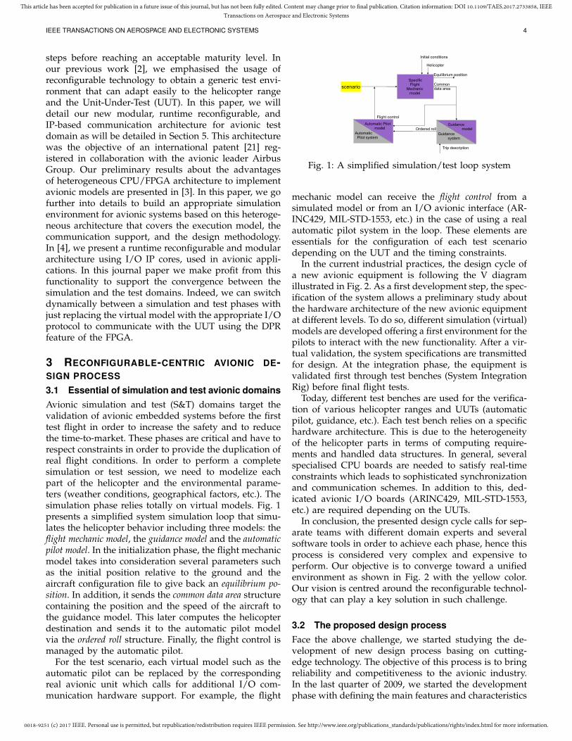
3.1 Essential of simulation and test avionic domainsAvionic simulation and test (S&T) domains target thevalidation of avionic embedded systems before the firsttest flight in order to increase the safety and to reducethe time-to-market. These phases are critical and have torespect constraints in order to provide the duplication ofreal flight conditions. In order to perform a completesimulation or test session, we need to modelize eachpart of the helicopter and the environmental parame-ters (weather conditions, geographical factors, etc.). Thesimulation phase relies totally on virtual models. Fig. 1presents a simplified system simulation loop that simu-lates the helicopter behavior including three models: theflight mechanic model, the guidance model and the automaticpilot model. In the initialization phase, the flight mechanicmodel takes into consideration several parameters suchas the initial position relative to the ground and theaircraft configuration file to give back an equilibrium po-sition. In addition, it sends the common data area structurecontaining the position and the speed of the aircraft tothe guidance model. This later computes the helicopterdestination and sends it to the automatic pilot modelvia the ordered roll structure. Finally, the flight control ismanaged by the automatic pilot.
For the test scenario, each virtual model such as theautomatic pilot can be replaced by the correspondingreal avionic unit which calls for additional I/O com-munication hardware support. For example, the flight
SpecificFlight
Mechanic model
Helicopter
Initial conditions
Equilibrium position
Common data area
Trip description
Ordered roll
Flight control
scenario
Flight control
Automatic Pilot model
Automatic Pilot system
Flight control
Guidance model
Guidance system
Fig. 1: A simplified simulation/test loop system
mechanic model can receive the flight control from asimulated model or from an I/O avionic interface (AR-INC429, MIL-STD-1553, etc.) in the case of using a realautomatic pilot system in the loop. These elements areessentials for the configuration of each test scenariodepending on the UUT and the timing constraints.
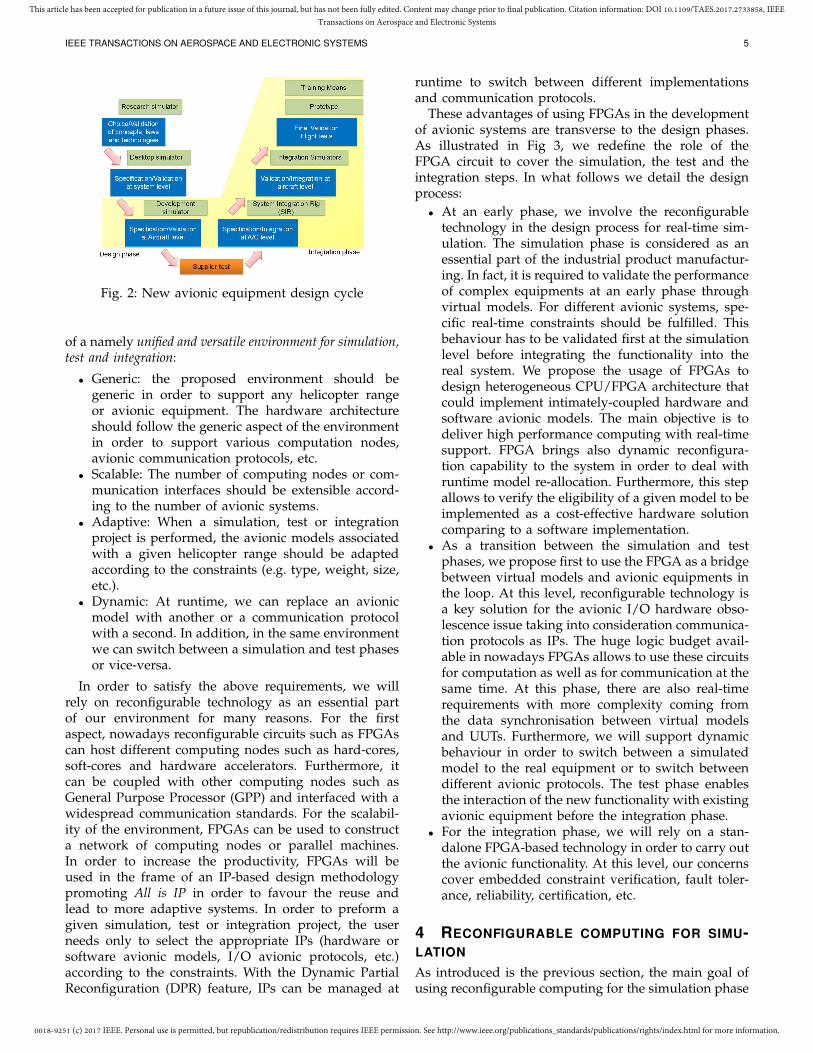
In the current industrial practices, the design cycle ofa new avionic equipment is following the V diagramillustrated in Fig. 2. As a first development step, the spec-ification of the system allows a preliminary study aboutthe hardware architecture of the new avionic equipmentat different levels. To do so, different simulation (virtual)models are developed offering a first environment for thepilots to interact with the new functionality. After a vir-tual validation, the system specifications are transmittedfor design. At the integration phase, the equipment isvalidated first through test benches (System IntegrationRig) before final flight tests.
Today, different test benches are used for the verifica-tion of various helicopter ranges and UUTs (automaticpilot, guidance, etc.). Each test bench relies on a specifichardware architecture. This is due to the heterogeneityof the helicopter parts in terms of computing require-ments and handled data structures. In general, severalspecialised CPU boards are needed to satisfy real-timeconstraints which leads to sophisticated synchronizationand communication schemes. In addition to this, ded-icated avionic I/O boards (ARINC429, MIL-STD-1553,etc.) are required depending on the UUTs.
In conclusion, the presented design cycle calls for sep-arate teams with different domain experts and severalsoftware tools in order to achieve each phase, hence thisprocess is considered very complex and expensive toperform. Our objective is to converge toward a unifiedenvironment as shown in Fig. 2 with the yellow color.Our vision is centred around the reconfigurable technol-ogy that can play a key solution in such challenge.
3.2 The proposed design processFace the above challenge, we started studying the de-velopment of new design process basing on cutting-edge technology. The objective of this process is to bringreliability and competitiveness to the avionic industry.In the last quarter of 2009, we started the developmentphase with defining the main features and characteristics
0018-9251 (c) 2017 IEEE. Personal use is permitted, but republication/redistribution requires IEEE permission. See http://www.ieee.org/publications_standards/publications/rights/index.html for more information.
This article has been accepted for publication in a future issue of this journal, but has not been fully edited. Content may change prior to final publication. Citation information: DOI 10.1109/TAES.2017.2733858, IEEETransactions on Aerospace and Electronic Systems
IEEE TRANSACTIONS ON AEROSPACE AND ELECTRONIC SYSTEMS 5
3. UN MODÈLE D’EXÉCUTION DYNAMIQUE POUR LESARCHITECTURES HÉTÉROGÈNES DÉDIÉ AU TEST ET À LASIMULATION
effectuées devront donc tenir compte des propriétés et des capacités du support matérielproposé.
3.3 Vers une nouvelle génération de systèmes de test et
de simulation
Dans cette nouvelle section, nous allons présenter notre réflexion concernant les capa-cités des futurs systèmes de test et de simulation.
3.3.1 Vers une mutualisation des moyens de test et de simulation
Figure 3.1 – Influence sur le cycle de développement d’un nouvel équipement
Dans le but d’accélérer le cycle de développement des nouveaux équipements ainsi quedes hélicoptères, nous avons proposé dans le cadre de cette thèse de mutualiser les moyensde test et de simulation. Dans un premier temps, cette mutualisation a un fort impactfinancier. En effet, le coût d’une heure de test en vol est le même que celui de quarante
34
Fig. 2: New avionic equipment design cycle
of a namely unified and versatile environment for simulation,test and integration:
• Generic: the proposed environment should begeneric in order to support any helicopter rangeor avionic equipment. The hardware architectureshould follow the generic aspect of the environmentin order to support various computation nodes,avionic communication protocols, etc.
• Scalable: The number of computing nodes or com-munication interfaces should be extensible accord-ing to the number of avionic systems.
• Adaptive: When a simulation, test or integrationproject is performed, the avionic models associatedwith a given helicopter range should be adaptedaccording to the constraints (e.g. type, weight, size,etc.).
• Dynamic: At runtime, we can replace an avionicmodel with another or a communication protocolwith a second. In addition, in the same environmentwe can switch between a simulation and test phasesor vice-versa.
In order to satisfy the above requirements, we willrely on reconfigurable technology as an essential partof our environment for many reasons. For the firstaspect, nowadays reconfigurable circuits such as FPGAscan host different computing nodes such as hard-cores,soft-cores and hardware accelerators. Furthermore, itcan be coupled with other computing nodes such asGeneral Purpose Processor (GPP) and interfaced with awidespread communication standards. For the scalabil-ity of the environment, FPGAs can be used to constructa network of computing nodes or parallel machines.In order to increase the productivity, FPGAs will beused in the frame of an IP-based design methodologypromoting All is IP in order to favour the reuse andlead to more adaptive systems. In order to preform agiven simulation, test or integration project, the userneeds only to select the appropriate IPs (hardware orsoftware avionic models, I/O avionic protocols, etc.)according to the constraints. With the Dynamic PartialReconfiguration (DPR) feature, IPs can be managed at
runtime to switch between different implementationsand communication protocols.
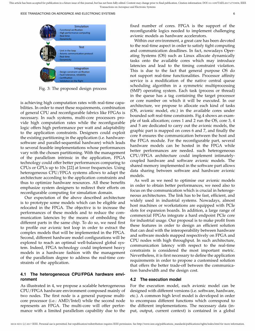
These advantages of using FPGAs in the developmentof avionic systems are transverse to the design phases.As illustrated in Fig 3, we redefine the role of theFPGA circuit to cover the simulation, the test and theintegration steps. In what follows we detail the designprocess:
• At an early phase, we involve the reconfigurabletechnology in the design process for real-time sim-ulation. The simulation phase is considered as anessential part of the industrial product manufactur-ing. In fact, it is required to validate the performanceof complex equipments at an early phase throughvirtual models. For different avionic systems, spe-cific real-time constraints should be fulfilled. Thisbehaviour has to be validated first at the simulationlevel before integrating the functionality into thereal system. We propose the usage of FPGAs todesign heterogeneous CPU/FPGA architecture thatcould implement intimately-coupled hardware andsoftware avionic models. The main objective is todeliver high performance computing with real-timesupport. FPGA brings also dynamic reconfigura-tion capability to the system in order to deal withruntime model re-allocation. Furthermore, this stepallows to verify the eligibility of a given model to beimplemented as a cost-effective hardware solutioncomparing to a software implementation.
• As a transition between the simulation and testphases, we propose first to use the FPGA as a bridgebetween virtual models and avionic equipments inthe loop. At this level, reconfigurable technology isa key solution for the avionic I/O hardware obso-lescence issue taking into consideration communica-tion protocols as IPs. The huge logic budget avail-able in nowadays FPGAs allows to use these circuitsfor computation as well as for communication at thesame time. At this phase, there are also real-timerequirements with more complexity coming fromthe data synchronisation between virtual modelsand UUTs. Furthermore, we will support dynamicbehaviour in order to switch between a simulatedmodel to the real equipment or to switch betweendifferent avionic protocols. The test phase enablesthe interaction of the new functionality with existingavionic equipment before the integration phase.
• For the integration phase, we will rely on a stan-dalone FPGA-based technology in order to carry outthe avionic functionality. At this level, our concernscover embedded constraint verification, fault toler-ance, reliability, certification, etc.
4 RECONFIGURABLE COMPUTING FOR SIMU-LATION
As introduced is the previous section, the main goal ofusing reconfigurable computing for the simulation phase
0018-9251 (c) 2017 IEEE. Personal use is permitted, but republication/redistribution requires IEEE permission. See http://www.ieee.org/publications_standards/publications/rights/index.html for more information.
This article has been accepted for publication in a future issue of this journal, but has not been fully edited. Content may change prior to final publication. Citation information: DOI 10.1109/TAES.2017.2733858, IEEETransactions on Aerospace and Electronic Systems
IEEE TRANSACTIONS ON AEROSPACE AND ELECTRONIC SYSTEMS 6
!
!"#$%&'()*+*,$)-'()&%*./0"1-&'()**+*2"34*5/06(0#&)-/*-(#5$')3*+*7/&%+'#/*+*89)&#"-":9**
;/<:*+*=)":*")*:4/*%((5**+*>."()"-*-(##$)"-&'()*50(:(-(%*+*7/&%+'#/*+*89)&#"-":9**
?):/30&'()*+ *8/<"3)*-()<:0&"):*./0"1-&'()*+ *,&$%:*:(%/0&)-/@*0/%"&A"%":9*+*B/0'1-&'()*+ *C&%"D&'()*()*:4/*E"34:*
Fig. 3: The proposed design process
is achieving high computation rates with real-time capa-bilities. In order to meet these requirements, combinationof general CPU and reconfigurable fabrics like FPGAs isnecessary. In such systems, multi-core processors pro-vide high computation rates while the reconfigurablelogic offers high performance per watt and adaptabilityto the application constraints. Designers could exploitthe existing partitioning in the application (i.e. hardware-software and parallel-sequential hardware) which leadsto several feasible implementations whose performancesvary with the chosen partitioning. With the managementof the parallelism intrinsic in the application, FPGAtechnology could offer better performances comparing toCPUs or GPUs up to 10x [22] at lower frequencies. Usingheterogeneous CPU/FPGA systems allows to adapt thearchitecture according to the application constraints andthus to optimize hardware resources. All these benefitsemphasize system designers to redirect their efforts onreconfigurable computing for simulation domain.
Our expectation of the above described architectureis to prototype some models which can be eligible andrelocated in the FPGA. The objective is to increase theperformances of these models and to reduce the com-munication latencies by the means of embedding thedifferent parts in the same chip. To do so, we need firstto profile our avionic test loop in order to extract thecomplex models that will be implemented in the FPGA.Second, different hardware model configurations will beexplored to reach an optimal well-balanced global sys-tem. Indeed, FPGA technology could implement heavymodels in a hardware fashion with the managementof the parallelism degree to address the real-time con-straints of the application.
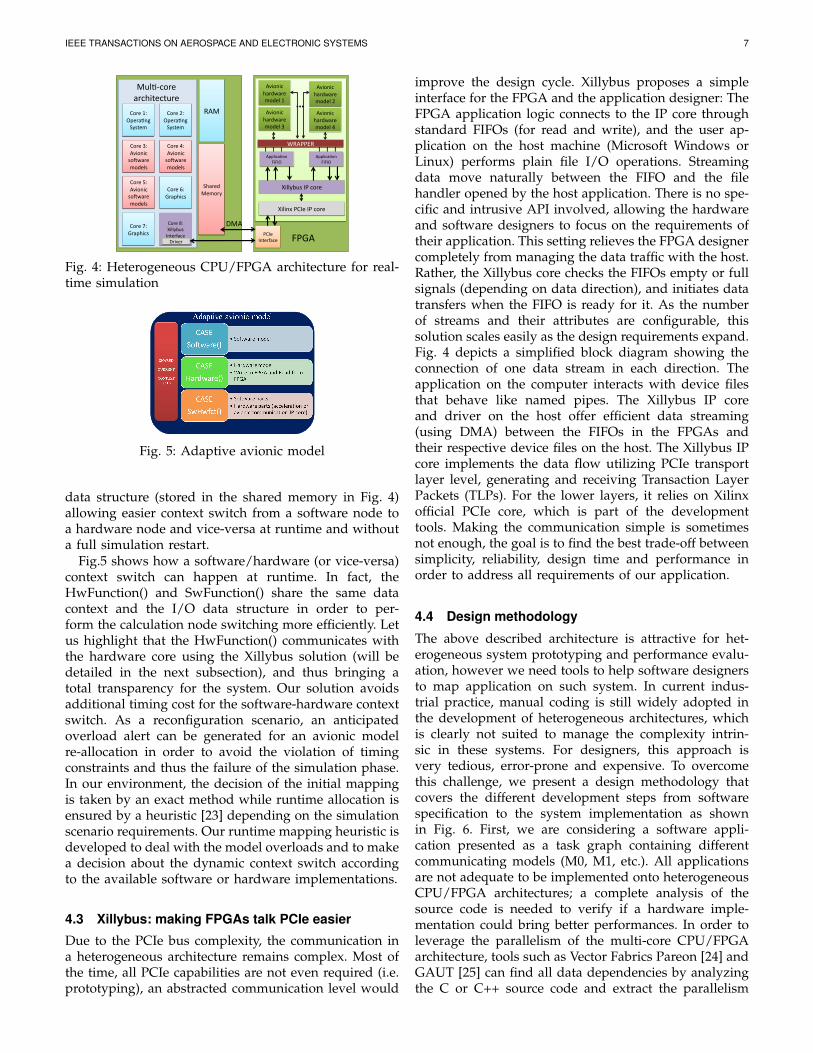
4.1 The heterogeneous CPU/FPGA hardware envi-ronmentAs illustrated in 4, we propose a scalable heterogeneousCPU/FPGA hardware environment composed mainly oftwo nodes. The first node is a general purpose multi-core processor (i.e.: AMD/Intel) while the second noderepresents an FPGA. The multi-core will offer perfor-mance with a limited parallelism capability due to the
fixed number of cores. FPGA is the support of thereconfigurable logics needed to implement challengingavionic models as hardware accelerators.
Within our environment, a great care has been devotedto the real-time aspect in order to satisfy tight computingand communication deadlines. In fact, nowadays Oper-ating Systems (OS) such as Linux allocate dynamicallytasks onto the available cores which may introducelatencies and lead to the timing constraint violation.This is due to the fact that general purpose OS donot support real-time functionalities. Processor affinityservice is a modification of the native central queuescheduling algorithm in a symmetric multiprocessing(SMP) operating system. Each task (process or thread)in the queue has a tag containing the target processoror core number on which it will be executed. In ourarchitecture, we propose to allocate each kind of tasks(OS, avionic model, etc.) in the available cores underbounded soft real-time constraints. Fig.4 shows an exam-ple of task allocation; cores 1 and 2 run the OS, core 3, 4and 5 are dedicated to carry out the avionic models, thegraphic part is mapped on cores 6 and 7, and finally thecore 8 ensures the communication between the host andthe FPGA module. For the reconfigurable part, severalhardware models can be hosted in the FPGA whilebetter performances are needed. such heterogeneousCPU/FPGA architecture could implement intimately-coupled hardware and software avionic models. Theshared memory implemented in the software part allowsdata sharing between software and hardware avionicmodels.
As well as we need to optimise our avionic modelsin order to obtain better performances, we need also tofocus on the communication which is crucial in heteroge-neous architectures. The link has to be fast, efficient, andwidely used in industrial systems. Nowadays, almosthost machines or workstations are equipped with PCIeslots for expansion boards. In addition, a large range ofcommercial FPGAs integrate a hard endpoint PCIe corefor industrial usage. Our proposal is to make profit fromthese features in order to design an efficient solutionthat can deal with the interoperability between hardwareand software models mapped respectively on FPGA andCPU nodes with high throughput. In such architecture,communication latency with respect to the real-timeconstraints is considered the most important metric.Nevertheless, it is first necessary to define the applicationrequirements in order to propose a customised solutionthat offers the better trade-off between the communica-tion bandwidth and the design cost.
4.2 The execution modelFor the execution model, each avionic model can bedesigned with different versions (i.e. software, hardware,etc.). A common high level model is developed in orderto encompass different functions which correspond tothe different implementations. The necessary data (in-put, output, current context) is contained in a global
IEEE TRANSACTIONS ON AEROSPACE AND ELECTRONIC SYSTEMS 7
!"#$%&'%()$#*+,-%./01$2%
!"#$%3'%456",67%0"89*#$%2":$;0%
!"#$%<'%456",67%0"89*#$%2":$;0%
!"#$%='%>#*)?670%
!"#$%@'%()$#*+,-%./01$2%
!"#$%A'%456",67%0"89*#$%2":$;0%
!"#$%B'%>#*)?670%
!"#$%C'%D6;;/EF0%G,1$#H*7$%
I4J%
.?*#$:%J$2"#/%
%%%%%%%%%%%%%%%%%%%%%%%%%%%%%%%%%%%%%%%%%%%%%K!G$%
G,1$#H*7$%
456",67%?*#:9*#$%2":$;%&%
456",67%?*#:9*#$%2":$;%3%
D6;6,L%K!G$%GK%7"#$%
JF;+M7"#$%*#7?61$71F#$%
NJ4%
OK>4%
!"
N#65$#%
456",67%?*#:9*#$%2":$;%@%
456",67%?*#:9*#$%2":$;%A%
D6;;/EF0%GK%7"#$%
4));67*+",%OGOG(%
4));67*+",%OGOG(%
PI4KKQI%
Fig. 4: Heterogeneous CPU/FPGA architecture for real-time simulation
Fig. 5: Adaptive avionic model
data structure (stored in the shared memory in Fig. 4)allowing easier context switch from a software node toa hardware node and vice-versa at runtime and withouta full simulation restart.
Fig.5 shows how a software/hardware (or vice-versa)context switch can happen at runtime. In fact, theHwFunction() and SwFunction() share the same datacontext and the I/O data structure in order to per-form the calculation node switching more efficiently. Letus highlight that the HwFunction() communicates withthe hardware core using the Xillybus solution (will bedetailed in the next subsection), and thus bringing atotal transparency for the system. Our solution avoidsadditional timing cost for the software-hardware contextswitch. As a reconfiguration scenario, an anticipatedoverload alert can be generated for an avionic modelre-allocation in order to avoid the violation of timingconstraints and thus the failure of the simulation phase.In our environment, the decision of the initial mappingis taken by an exact method while runtime allocation isensured by a heuristic [23] depending on the simulationscenario requirements. Our runtime mapping heuristic isdeveloped to deal with the model overloads and to makea decision about the dynamic context switch accordingto the available software or hardware implementations.
4.3 Xillybus: making FPGAs talk PCIe easier
Due to the PCIe bus complexity, the communication ina heterogeneous architecture remains complex. Most ofthe time, all PCIe capabilities are not even required (i.e.prototyping), an abstracted communication level would
improve the design cycle. Xillybus proposes a simpleinterface for the FPGA and the application designer: TheFPGA application logic connects to the IP core throughstandard FIFOs (for read and write), and the user ap-plication on the host machine (Microsoft Windows orLinux) performs plain file I/O operations. Streamingdata move naturally between the FIFO and the filehandler opened by the host application. There is no spe-cific and intrusive API involved, allowing the hardwareand software designers to focus on the requirements oftheir application. This setting relieves the FPGA designercompletely from managing the data traffic with the host.Rather, the Xillybus core checks the FIFOs empty or fullsignals (depending on data direction), and initiates datatransfers when the FIFO is ready for it. As the numberof streams and their attributes are configurable, thissolution scales easily as the design requirements expand.Fig. 4 depicts a simplified block diagram showing theconnection of one data stream in each direction. Theapplication on the computer interacts with device filesthat behave like named pipes. The Xillybus IP coreand driver on the host offer efficient data streaming(using DMA) between the FIFOs in the FPGAs andtheir respective device files on the host. The Xillybus IPcore implements the data flow utilizing PCIe transportlayer level, generating and receiving Transaction LayerPackets (TLPs). For the lower layers, it relies on Xilinxofficial PCIe core, which is part of the developmenttools. Making the communication simple is sometimesnot enough, the goal is to find the best trade-off betweensimplicity, reliability, design time and performance inorder to address all requirements of our application.
4.4 Design methodology
The above described architecture is attractive for het-erogeneous system prototyping and performance evalu-ation, however we need tools to help software designersto map application on such system. In current indus-trial practice, manual coding is still widely adopted inthe development of heterogeneous architectures, whichis clearly not suited to manage the complexity intrin-sic in these systems. For designers, this approach isvery tedious, error-prone and expensive. To overcomethis challenge, we present a design methodology thatcovers the different development steps from softwarespecification to the system implementation as shownin Fig. 6. First, we are considering a software appli-cation presented as a task graph containing differentcommunicating models (M0, M1, etc.). All applicationsare not adequate to be implemented onto heterogeneousCPU/FPGA architectures; a complete analysis of thesource code is needed to verify if a hardware imple-mentation could bring better performances. In order toleverage the parallelism of the multi-core CPU/FPGAarchitecture, tools such as Vector Fabrics Pareon [24] andGAUT [25] can find all data dependencies by analyzingthe C or C++ source code and extract the parallelism

0018-9251 (c) 2017 IEEE. Personal use is permitted, but republication/redistribution requires IEEE permission. See http://www.ieee.org/publications_standards/publications/rights/index.html for more information.
This article has been accepted for publication in a future issue of this journal, but has not been fully edited. Content may change prior to final publication. Citation information: DOI 10.1109/TAES.2017.2733858, IEEETransactions on Aerospace and Electronic Systems
IEEE TRANSACTIONS ON AEROSPACE AND ELECTRONIC SYSTEMS 8le profilage d’un modèle jusqu’à l’implémentation sur sa cible d’exécution matérielle. Eneffet, pour surmonter les difficultés liées à ce type de conception, nous avons proposé uneméthodologie [6] décrite dans la figure 4.8.
Figure 4.8 – Méthodologie de développement
Tout d’abord, il est nécessaire de spécifier un projet de simulation présenté commeun graphe de tâches contenant différents modèles communicants (M0, M1, etc.). Tous lesprojets n’étant pas adaptés à une exécution performante sur architecture CPU-FPGA,il est nécessaire d’effectuer une analyse complète du code source afin de déterminer sonpotentiel de parallélisation.Pour ce faire, des outils d’analyse tels que Pareon [67] proposé par la société Vector Fabrics,Intel Parallel Studio [33] ainsi que GAUT [19] sont aujourd’hui disponibles. Ces outilseffectuent généralement une compilation de ce code source pour une analyse bas niveaude ce dernier. Ainsi, il devient possible de situer les dépendances de données et ainsid’extraire le degré de parallélisation comme nous pouvons le constater sur la figure 4.9. Surcette figure, nous pouvons observer le résultat d’une analyse d’un code par l’outil Pareonprésentant plusieurs boucles. Deux de ces boucles présentent une faible dépendance dedonnées entre les différentes itérations, dès lors en répartissant leur exécution sur plusieursthreads, il est possible de réduire leur temps d’exécution. Dans l’exemple présent sur cette
65
Fig. 6: Application design methodology for heteroge-neous CPU/FPGA system
intrinsic in the application. Pareon analyses partitionsand maps applications on specific platforms as hetero-geneous ones. It can also estimate the performance of theparallelized software before implementing it. Moreover,it can trim any overhead in your hardware to reduce costand ensure that all critical behaviours in your programare exercised. After this analysis, the developer willhave key information for source code optimization. Toperform the application mapping, system resources andapplication constraints are needed. This step requiresa specific heuristic method to resolve a multi-objectiveexploration problem. After the mapping step, we needto develop some user hardware applications from theexisting models (M1, M2, etc.). To make this step moreefficient, tools such as Riverside Optimizing Compilerfor Configurable Computing (ROCCC) [26] can focus onFPGA-based code acceleration from a subset of the Clanguage. ROCCC does not focus on the generation ofarbitrary hardware circuits. Its objectives are to max-imize parallelism within the constraints of the targetdevice, optimize clock cycle time by efficient pipelining,and minimize the area utilized. It uses extensive andunique loop analysis techniques to increase the reuseof data fetched from off-chip memory. The communi-cation synthesis step consists of generating the requiredCPU-to-CPU or CPU-to-FPGA communication interfacesdepending on the selected mapping. Having all sourcecode for a CPU/FPGA implementation, the compilationstep, using GCC and ISE from Xilinx can be easilyperformed in order to map all the application onto thesystem.
5 RECONFIGURABLE COMPUTING FOR TEST
As stated in Section 3.1, the test avionic domain calls foran additional hardware in order to communicate withavionic equipments. In current industrial practices, oneof the biggest challenges of relying on different PCBs(Printed Circuit Boards) for different requirements, is thehardware obsolescence issue. Ever-changing applicationrequirements demand the customization of the I/O businterfaces. Changing the hardware meant redesigning
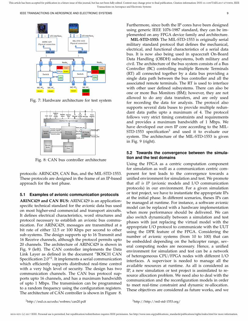
the entire board, with a lot of Non-Recurring Engineer-ing (NRE) cost and significant time-to-market. The VITA(VMEbus International Trade Association group) FMC(FPGA Mezzanine Card) standard solves the I/O obso-lescence issue partially, with a single 400-pin connectorwith a potential overall bandwidth of 40 Gb/s. Thisessentially means that the I/O bus interface of a PCB isdesigned separately as a module and interfaced with theboard using the FMC connector. Thus, every time an I/Obus interface needs a change, just the module changes,thereby avoiding a complete redesign. For the test phase,the FPGAs can be used for more than just computationalpurpose in order to improve the system performance.The introduction of FMC I/O standard has given a newpurpose for FPGAs to be used as a communicationplatform. Taking into account the features offered byFPGAs and FMCs, such as flexibility and modularity,we have redefined the role of these devices to be usedas a generic communication and computation-centricplatform. Thus, in addition to the avionic models, FPGAswill implement I/O IPs such as ARINC429 in order toperform the communication with the UUT.
A new modular, runtime reconfigurable, IntellectualProperty (IP)-based communication-centric hardware isproposed for avionic test application domain as illus-trated in Fig. 7. The hardware architecture is composedof standard machines running virtual avionic modelscoupled with FPGA boards equipped with FMC connec-tors. These connectors ensure through the I/O interfacejust the physical connection with the avionic equipment.The communication protocol is implemented as an IPhosted on the FPGA and data are transmitted via theFMC. Thus, the test phase for a given equipment requiresthe instantiation of the appropriate I/O IP protocolwhile the other avionic models remain virtual. Somemodels can be also hosted on the FPGA as the samelevel of the I/O IPs which can reduce significantly thecommunication delays. We can rely on several FPGAboards in order to consider several avionic UUT on theloop.
With such architecture, avionic IP cores can be ex-plored by system designers in different scenarios de-pending on the application requirement. Therefore, de-pending on the test scenario, the user can choose a com-munication IP core to be configured dynamically. Thisremoves the need to have multiple/redundant systems,each for a different protocol. Moreover, when the IPcore is reconfigured, the communication channels withthe FMC is also reconfigured dynamically along withthe protocol. In case the FMC module does not providea corresponding interface for the communication corebeing reconfigured (which can be detected using the I2CEEPROM in the FMC module), it can be swapped withanother appropriate FMC module. Thus eliminating theneed to redesign the entire board based on a new I/Ointerface requirement.
In the next sub-sections, we will detail the implemen-tation of three widely used avionic I/O communication
0018-9251 (c) 2017 IEEE. Personal use is permitted, but republication/redistribution requires IEEE permission. See http://www.ieee.org/publications_standards/publications/rights/index.html for more information.
This article has been accepted for publication in a future issue of this journal, but has not been fully edited. Content may change prior to final publication. Citation information: DOI 10.1109/TAES.2017.2733858, IEEETransactions on Aerospace and Electronic Systems
IEEE TRANSACTIONS ON AEROSPACE AND ELECTRONIC SYSTEMS 9
!"#$%&'()*$
+",-$
!"#$"%& !"#$"'&
()*+'&
!"#$%&'()*$
+",-$
!"#$"%&
()*+,&
-&
!"#$"'&
-& -&
.$&/,0& .$&'112&
!)*+3'&
.45&678+9:;<+'&
!)*+32&
!)*+3,&
!)*+3=&
!)*+3>&
!)*+31&
?6@+9& ?6@+9&
!)*+3/&
-&
!)*+3A&
.45&678+9:;<+,&
-./0!$123$"*45')67$)899:)('89$$
;/<=%>?$@AAB$"*45')67$)899:)('89$$
+;!$578($ +;!$578($
Fig. 7: Hardware architecture for test system
!"#$%&'($)*'"'+$,$"#)-.+/()
0%'"1,/#)234$%)
5$($/6$)234$%)
2/#)7#%$',)8%.($11/"+)
9(($:#'"($);/<#$%)
2/#)0/,/"+))-.+/()
!"#$%&'()&*%%#+*,!"#$%&'()"*-.*%(,
!"#$%&'()%(#(.%,
/#"0)%1$2)*$,
3.%)0"'4*,
3.%&5$,
6#&78*)75'$(,
28529, "*%*(,
:*+'%(*",;"'(*,,<$#=8*,
:*+'%(*",6*8*2(,
!>,,?*%%#+*,
:>,,:*#0,<$#=8*,
:*+'%(*",@#(#,
:>,,?*%%#+*,
6(#(.%,:*+'%(*",
!"#$%&'()0#(#,
:*2*'4*)0#(#,
Fig. 8: CAN bus controller architecture
protocols: ARINC429, CAN Bus, and the MIL-STD-1553.These protocols are designed in the frame of an IP-basedapproach for the test phase.
5.1 Examples of avionic communication protocolsARINC429 and CAN BUS: ARINC429 is an application-specific technical standard for the avionic data bus usedon most higher-end commercial and transport aircrafts.It defines electrical characteristics, word structures andprotocol necessary to establish an avionic bus commu-nication. For ARINC429, messages are transmitted at abit rate of either 12.5 or 100 Kbps per second to othersub-systems. The design supports up to 16 Transmit and16 Receive channels, although the protocol permits upto20 channels. The architecture of ARINC429 is shown inFig. 9 (left). The CAN controller implements the DataLink Layer as defined in the document ”BOSCH CANSpecification 2.0”2. It implements a serial communicationwhich efficiently supports distributed real-time controlwith a very high level of security. The design has twocommunication channels. The CAN bus protocol sup-ports upto 16 channels, and has a maximum bandwidthof upto 1 Mbps. The transmission can be programmedto a random frequency using the configuration registers.The architecture of CAN controller is shown in Figure 8.
2http://esd.cs.ucr.edu/webres/can20.pdf
Furthermore, since both the IP cores have been designedusing generic IEEE 1076-1987 standard, they can be im-plemented on any FPGA device family and architecture.
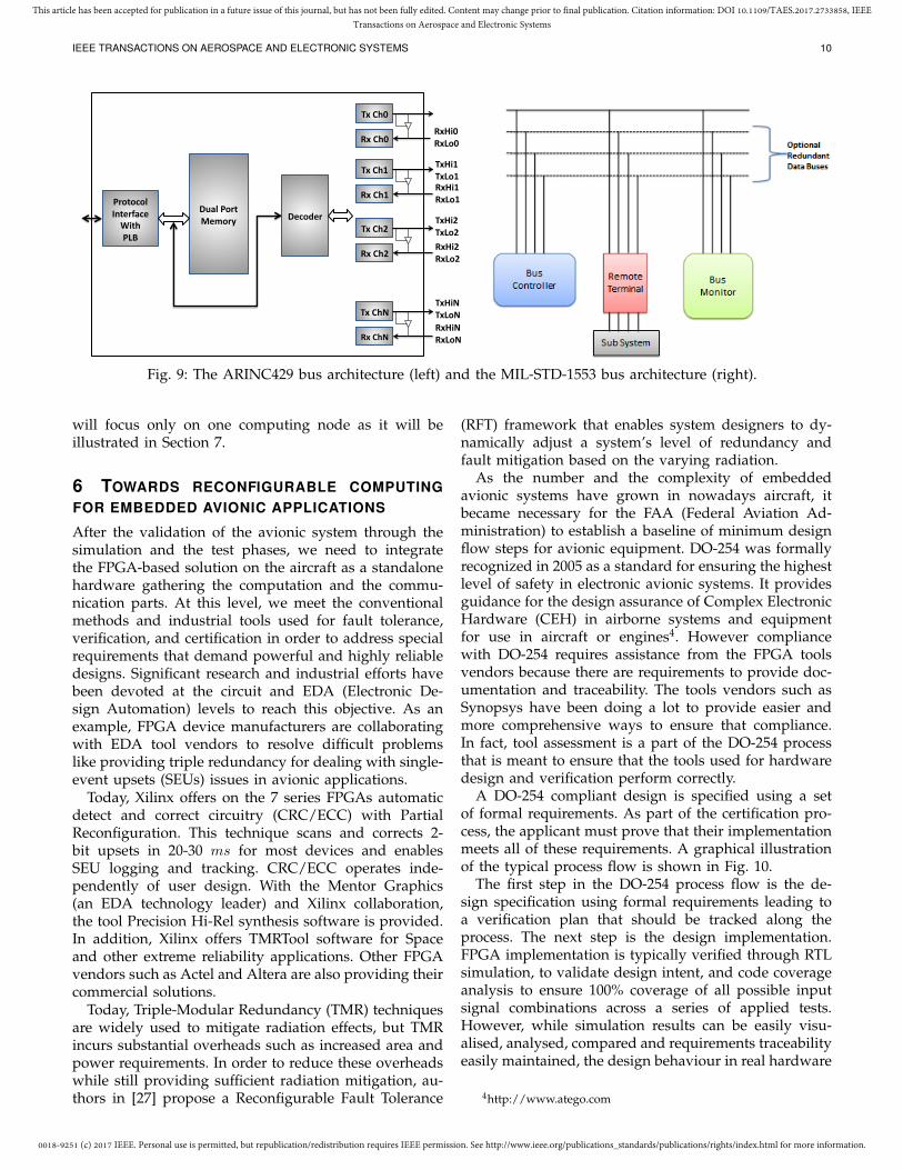
MIL-STD-1553: The MIL-STD-1553 is originally serialmilitary standard protocol that defines the mechanical,electrical, and functional characteristics of a serial databus. It is now also being used in spacecraft On-BoardData Handling (OBDH) subsystems, both military andcivil. The architecture of the bus system consists of a BusController (BC) controlling multiple Remote Terminals(RT) all connected together by a data bus providing asingle data path between the bus controller and all theassociated remote terminals. The RT is used to interfacewith other user defined subsystems. There can also beone or more Bus Monitors (BM); however, they are notallowed to do any data transfers, and are only usedfor recording the data for analysis. The protocol alsosupports several data buses to provide multiple redun-dant data paths upto a maximum of 4. The protocolfollows very strict timing constraints and requirementsand provides a maximum bandwidth of 1 Mbps. Wehave developed our own IP core according to the MIL-STD-1553 specification3 and used it to evaluate oursystem. The architecture of the MIL-STD-1553 is givenin Fig. 9 (right).
5.2 Towards the convergence between the simula-tion and the test domainsUsing the FPGA as a centric computation componentfor simulation as well as a communication centric com-ponent for test leads to the convergence towards aunified environment for simulation and test. We promotethat all is IP (avionic models and I/O communicationprotocols) in our environment. For a given simulationor test project, we have to instantiate the appropriate IPsat the initial phase. In different scenarios, theses IPs canbe managed at runtime. For instance, a software avionicmodel can be replaced with a hardware implementationwhen more performance should be delivered. We canalso switch dynamically between a simulation and testphases with just replacing the virtual model with theappropriate I/O protocol to communicate with the UUTusing the DPR feature of the FPGA. Considering thenumber of avionic systems (from 10 to 100) that canbe embedded depending on the helicopter range, sev-eral computing nodes are necessary. Hence, a unifiedenvironment for simulation and test can be a networkof heterogeneous CPU/FPGA nodes with different I/Ointerfaces. A supervisor is needed to manage all theavailable resources at runtime. As all is considered asIP, a new simulation or test project is assimilated to re-source allocation problem. We need also to deal with thecommunication and the reconfiguration models in orderto meet real-time constraint and dynamic re-allocation.These objectives are considered as future works, and we
3http://http://mil-std-1553.org/
0018-9251 (c) 2017 IEEE. Personal use is permitted, but republication/redistribution requires IEEE permission. See http://www.ieee.org/publications_standards/publications/rights/index.html for more information.
This article has been accepted for publication in a future issue of this journal, but has not been fully edited. Content may change prior to final publication. Citation information: DOI 10.1109/TAES.2017.2733858, IEEETransactions on Aerospace and Electronic Systems
IEEE TRANSACTIONS ON AEROSPACE AND ELECTRONIC SYSTEMS 10
!"#$%&'()%*+,'(-%
&(')'.'$%%/0)+(1#.+%%23)4%%&56%
!+.'7+(%
89%:4;%
<9%:4;%
89%:4=%
<9%:4=%
89%:4>%
<9%:4>%
89%:4?%
<9%:4?%
89@3=%895'=%
89@3>%895'>%
89@3?%895'?%
<9@3;%<95';%
<9@3=%<95'=%
<9@3>%<95'>%
<9@3?%<95'?%
!Fig. 9: The ARINC429 bus architecture (left) and the MIL-STD-1553 bus architecture (right).
will focus only on one computing node as it will beillustrated in Section 7.
6 TOWARDS RECONFIGURABLE COMPUTINGFOR EMBEDDED AVIONIC APPLICATIONS
After the validation of the avionic system through thesimulation and the test phases, we need to integratethe FPGA-based solution on the aircraft as a standalonehardware gathering the computation and the commu-nication parts. At this level, we meet the conventionalmethods and industrial tools used for fault tolerance,verification, and certification in order to address specialrequirements that demand powerful and highly reliabledesigns. Significant research and industrial efforts havebeen devoted at the circuit and EDA (Electronic De-sign Automation) levels to reach this objective. As anexample, FPGA device manufacturers are collaboratingwith EDA tool vendors to resolve difficult problemslike providing triple redundancy for dealing with single-event upsets (SEUs) issues in avionic applications.
Today, Xilinx offers on the 7 series FPGAs automaticdetect and correct circuitry (CRC/ECC) with PartialReconfiguration. This technique scans and corrects 2-bit upsets in 20-30 ms for most devices and enablesSEU logging and tracking. CRC/ECC operates inde-pendently of user design. With the Mentor Graphics(an EDA technology leader) and Xilinx collaboration,the tool Precision Hi-Rel synthesis software is provided.In addition, Xilinx offers TMRTool software for Spaceand other extreme reliability applications. Other FPGAvendors such as Actel and Altera are also providing theircommercial solutions.
Today, Triple-Modular Redundancy (TMR) techniquesare widely used to mitigate radiation effects, but TMRincurs substantial overheads such as increased area andpower requirements. In order to reduce these overheadswhile still providing sufficient radiation mitigation, au-thors in [27] propose a Reconfigurable Fault Tolerance
(RFT) framework that enables system designers to dy-namically adjust a system’s level of redundancy andfault mitigation based on the varying radiation.
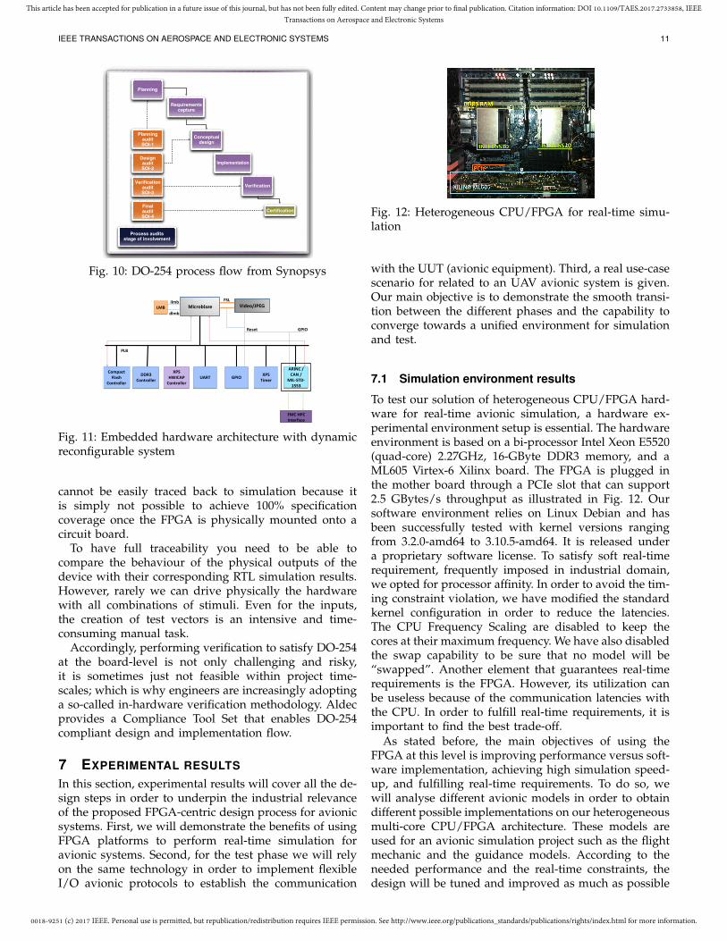
As the number and the complexity of embeddedavionic systems have grown in nowadays aircraft, itbecame necessary for the FAA (Federal Aviation Ad-ministration) to establish a baseline of minimum designflow steps for avionic equipment. DO-254 was formallyrecognized in 2005 as a standard for ensuring the highestlevel of safety in electronic avionic systems. It providesguidance for the design assurance of Complex ElectronicHardware (CEH) in airborne systems and equipmentfor use in aircraft or engines4. However compliancewith DO-254 requires assistance from the FPGA toolsvendors because there are requirements to provide doc-umentation and traceability. The tools vendors such asSynopsys have been doing a lot to provide easier andmore comprehensive ways to ensure that compliance.In fact, tool assessment is a part of the DO-254 processthat is meant to ensure that the tools used for hardwaredesign and verification perform correctly.
A DO-254 compliant design is specified using a setof formal requirements. As part of the certification pro-cess, the applicant must prove that their implementationmeets all of these requirements. A graphical illustrationof the typical process flow is shown in Fig. 10.
The first step in the DO-254 process flow is the de-sign specification using formal requirements leading toa verification plan that should be tracked along theprocess. The next step is the design implementation.FPGA implementation is typically verified through RTLsimulation, to validate design intent, and code coverageanalysis to ensure 100% coverage of all possible inputsignal combinations across a series of applied tests.However, while simulation results can be easily visu-alised, analysed, compared and requirements traceabilityeasily maintained, the design behaviour in real hardware
4http://www.atego.com
0018-9251 (c) 2017 IEEE. Personal use is permitted, but republication/redistribution requires IEEE permission. See http://www.ieee.org/publications_standards/publications/rights/index.html for more information.
This article has been accepted for publication in a future issue of this journal, but has not been fully edited. Content may change prior to final publication. Citation information: DOI 10.1109/TAES.2017.2733858, IEEETransactions on Aerospace and Electronic Systems
IEEE TRANSACTIONS ON AEROSPACE AND ELECTRONIC SYSTEMS 11
Understanding DO-254 Compliance for the Verification of Airborne Digital Hardware 2
Compliance to this standard involves a process that is more rigorous than the standard ASIC/FPGA design
and verification flow. While the tools used to design and verify the hardware are the same as in non-DO-254
applications, the process involves additional steps, particularly in the area of functional verification.
Parts of a compliant flowDO-254 applies to complex airborne hardware, such as ASICs, FPGAs, and PLDs. According to the
specification, a hardware item is considered “complex” if a comprehensive combination of deterministic tests
and analyses cannot ensure correct functional performance under all foreseeable operating conditions. For
complex devices, a rigorous, structured design and verification process takes the place of exhaustive testing.
Demonstrating that the development and verification of complex hardware complies with this process is the
objective of DO-254.
A DO-254 compliant design is specified using a set of formal requirements. As part of the certification
process, the applicant must prove that their implementation meets all of these requirements. A graphical
illustration of the typical process flow is shown in Figure 2.
Figure 2: DO-254 process flow
Note that the process described in this document is a template. Depending on the nature of the project,
different stages and/or tools may be required. A key principle, however, remains constant for successful
DO-254 compliant flows: verification results (simulation waveforms, regression status, coverage figures) must
be traceable and linked to the formal requirements. The process of traceability may be either automated or
manual; the output capabilities of the tools utilized in the flow will determine both the ease and degree of
automation.
Important points to note about DO-254DO-254 is, first and foremost, a process specification; it does not specify the detailed implementation of that
process. In particular, a very common misconception exists that there are “DO-254 Certified” tools available
– this is not the case as it is the overall process itself that receives certification, and not individual elements
Planning
Requirementscapture
Conceptualdesign
Verification
PlanningauditSOI-1
DesignauditSOI-2
VerificationauditSOI-3
FinalauditSOI-4
Process auditsstage of involvement
Implementation
Certification
Fig. 10: DO-254 process flow from Synopsys
!"#$%&'()*+
,%-.(#/+0'(12+
,%3/$%''*$+
4456+,%3/$%''*$+
789+:;<,=8+,%3/$%''*$+
>=5?+ @8<A+ 789+?"-*$+
=5<B,+C+,=B+C+
!<DE9?4EFGG6+
H"I*%CJ8K@+09D+
8DL+
5*1*/+
"'-&+
I'-&+D!L+
@8<A+
+++++0!,+:8,+++++++++++<3/*$M(#*+
Fig. 11: Embedded hardware architecture with dynamicreconfigurable system
cannot be easily traced back to simulation because itis simply not possible to achieve 100% specificationcoverage once the FPGA is physically mounted onto acircuit board.
To have full traceability you need to be able tocompare the behaviour of the physical outputs of thedevice with their corresponding RTL simulation results.However, rarely we can drive physically the hardwarewith all combinations of stimuli. Even for the inputs,the creation of test vectors is an intensive and time-consuming manual task.
Accordingly, performing verification to satisfy DO-254at the board-level is not only challenging and risky,it is sometimes just not feasible within project time-scales; which is why engineers are increasingly adoptinga so-called in-hardware verification methodology. Aldecprovides a Compliance Tool Set that enables DO-254compliant design and implementation flow.
7 EXPERIMENTAL RESULTS
In this section, experimental results will cover all the de-sign steps in order to underpin the industrial relevanceof the proposed FPGA-centric design process for avionicsystems. First, we will demonstrate the benefits of usingFPGA platforms to perform real-time simulation foravionic systems. Second, for the test phase we will relyon the same technology in order to implement flexibleI/O avionic protocols to establish the communication
6. ÉTUDE DE CAS ET VALIDATION EXPÉRIMENTALE
Figure 6.1 – Configuration matérielle
104
Fig. 12: Heterogeneous CPU/FPGA for real-time simu-lation
with the UUT (avionic equipment). Third, a real use-casescenario for related to an UAV avionic system is given.Our main objective is to demonstrate the smooth transi-tion between the different phases and the capability toconverge towards a unified environment for simulationand test.
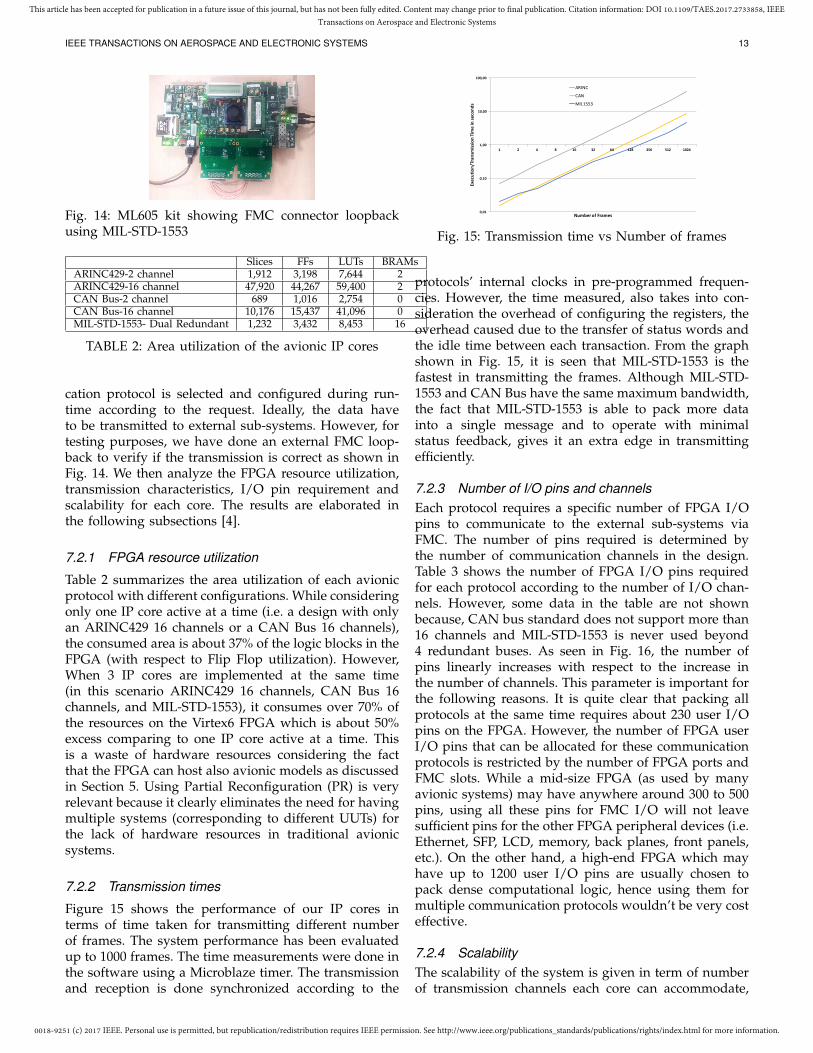
7.1 Simulation environment results
To test our solution of heterogeneous CPU/FPGA hard-ware for real-time avionic simulation, a hardware ex-perimental environment setup is essential. The hardwareenvironment is based on a bi-processor Intel Xeon E5520(quad-core) 2.27GHz, 16-GByte DDR3 memory, and aML605 Virtex-6 Xilinx board. The FPGA is plugged inthe mother board through a PCIe slot that can support2.5 GBytes/s throughput as illustrated in Fig. 12. Oursoftware environment relies on Linux Debian and hasbeen successfully tested with kernel versions rangingfrom 3.2.0-amd64 to 3.10.5-amd64. It is released undera proprietary software license. To satisfy soft real-timerequirement, frequently imposed in industrial domain,we opted for processor affinity. In order to avoid the tim-ing constraint violation, we have modified the standardkernel configuration in order to reduce the latencies.The CPU Frequency Scaling are disabled to keep thecores at their maximum frequency. We have also disabledthe swap capability to be sure that no model will be“swapped”. Another element that guarantees real-timerequirements is the FPGA. However, its utilization canbe useless because of the communication latencies withthe CPU. In order to fulfill real-time requirements, it isimportant to find the best trade-off.
As stated before, the main objectives of using theFPGA at this level is improving performance versus soft-ware implementation, achieving high simulation speed-up, and fulfilling real-time requirements. To do so, wewill analyse different avionic models in order to obtaindifferent possible implementations on our heterogeneousmulti-core CPU/FPGA architecture. These models areused for an avionic simulation project such as the flightmechanic and the guidance models. According to theneeded performance and the real-time constraints, thedesign will be tuned and improved as much as possible

0018-9251 (c) 2017 IEEE. Personal use is permitted, but republication/redistribution requires IEEE permission. See http://www.ieee.org/publications_standards/publications/rights/index.html for more information.
This article has been accepted for publication in a future issue of this journal, but has not been fully edited. Content may change prior to final publication. Citation information: DOI 10.1109/TAES.2017.2733858, IEEETransactions on Aerospace and Electronic Systems
IEEE TRANSACTIONS ON AEROSPACE AND ELECTRONIC SYSTEMS 12
Results Speed-up Maximumnumber ofuseful threads
Synchronizationoverhead
Model A 1.2 2 1%Model B 0 1 0%Model C 2.4 3 0%Model D 3.5 6 39%Model E 3 4 29%
TABLE 1: Avionic models analysis
in order to be executed more efficiently on our archi-tecture considering also switching at runtime betweensoftware and hardware configurations or vice-versa.
Table 1 summarizes the experimental results obtainedby analysing the software models with Pareon tool.First, we measure the speed-up obtained after opti-mization. Second, threads must be created for parallelimplementation strategy. This might be implementedthrough the use of POSIX calls creating the threads. Themaximum useful number of threads is directly linkedwith the parallelism degree of the application. Indeed,as shown by many parallelism laws, there is alwaysa limit number of useful calculation nodes, it is thesame for the maximum of useful threads. But multiplethreads means more data synchronisation. That meansa less time delay while waiting for data and thereforeless latency. Synchronization brings overhead, there isa trade-off between the latency introduced by doingfewer synchronizations with more data and the overheadintroduced by doing more synchronizations with lessdata. Pareon helps the user to get the best trade-off.
Pareon shows a 1.2 speed-up for the model A with lowsynchronization overhead with only two threads. ModelB cannot make profit from a parallelization strategy. Forthese two models better performances can be achievedjust with hardware implementation. Model C, D and Eoffer higher parallelism degree with low synchronisationoverhead for model C. These models are suitable formulti-core architecture or hybrid multi-core CPU/FPGAimplementation by splitting the models into differentfunctions due to the low synchronization overhead.
Using our previous results, we decide to implementmodel A which is the Flight Mechanic model in orderto observe the behaviour of such model in a VHDLhardware implementation. With the software version, weobtained a 20µs of execution time with our host.
For the hardware implementation, we target theVirtex-6 Xilinx board (ML605) as execution support. AVHDL implementation of the Flight Mechanic model offersa 2µs of execution time with 8% space occupation, thisis due mainly to the usage of floating point calculationin this model. This result offers the opportunity to movemodel A from a processor to the FPGA in the case oftiming constraint violation or an anticipated overload.
In the next experiment, we will consider the simu-lation loop presented in Fig. 1, the real-time period isset to 10 milliseconds. The Flight Mechanic model modelis implemented in hardware and hosted on the FPGA
�����
�����
����
����
�����
�����
�����
����
����
�����
����
�����
�����
����
�
��
�
��
��
��
��
��
��
��
��
� ������
��� ��
���
����
� � ����
Fig. 13: Time repartition of a multi-model soft/hardsimulation project
while the other models are executed on processor. Ourobjective is to verify the stability of the simulator accord-ing to the global system load. While the load increasesand upto certain limit, many runtime reconfigurationsoccur without any interruption of the simulation causedby a real-time period overflow. We highlight that theexecution time of a software model increases accordingto the processor load which is not the case of a hardwaremodel hosted on the FPGA.
Figure 13 describes simulation model time repartition.The execution time of the model is proportional to theprocessor’s load and inversely proportional to the “wait”duration. “Complete” corresponds to the percentage ofsuccessful simulation. Figure 13 shows that the I/Otime and the reconfiguration time are negligible. Assoon as the load exceeds the migration threshold (87%),migrations occur. Then, as the load continues to increasethe “too many consecutive migrations alert” occurs andstops the simulation which is due mainly to the soft-ware part. This result demonstrates that a heterogeneousCPU/FPGA architecture can be an efficient executionsupport for real-time simulation in avionic domain with-out referring to a dedicated and expensive solutions asdiscussed in Section 2. As a conclusion, we highlight thatthe FPGA can bring performance in such domain plyingmainly the role of a computing hardware accelerator.
7.2 Test environment resultsFor the test environment, we will rely on the sametechnology in order to establish the communication withthe UUT (avionic equipment) according to the genericarchitecture presented in Fig. 7. In fact, the ML605 boardthat we are using provides two FMC slots; one with aHigh Pin Count (HPC) and the other with a Low PinCount (LPC). Hence, these slots can be used to hostsimultaneously two different FMC cards presenting I/Oavionic interfaces as shown in Fig. 14. Different commu-nication avionic protocols (ARINC249/CAN/MIL-STD-1553) are implemented and tested in real scenarios. To doso, a Microblaze processor is used in order to configurethe registers and initiate data transfers. A number offrames is transmitted to an avionic sub-system using anappropriate communication protocol (ARINC429/CANBus/MIL-STD-1553) via a FMC interface. The communi-
0018-9251 (c) 2017 IEEE. Personal use is permitted, but republication/redistribution requires IEEE permission. See http://www.ieee.org/publications_standards/publications/rights/index.html for more information.
This article has been accepted for publication in a future issue of this journal, but has not been fully edited. Content may change prior to final publication. Citation information: DOI 10.1109/TAES.2017.2733858, IEEETransactions on Aerospace and Electronic Systems
IEEE TRANSACTIONS ON AEROSPACE AND ELECTRONIC SYSTEMS 13
!
Fig. 14: ML605 kit showing FMC connector loopbackusing MIL-STD-1553
Slices FFs LUTs BRAMsARINC429-2 channel 1,912 3,198 7,644 2ARINC429-16 channel 47,920 44,267 59,400 2CAN Bus-2 channel 689 1,016 2,754 0CAN Bus-16 channel 10,176 15,437 41,096 0MIL-STD-1553- Dual Redundant 1,232 3,432 8,453 16
TABLE 2: Area utilization of the avionic IP cores
cation protocol is selected and configured during run-time according to the request. Ideally, the data haveto be transmitted to external sub-systems. However, fortesting purposes, we have done an external FMC loop-back to verify if the transmission is correct as shown inFig. 14. We then analyze the FPGA resource utilization,transmission characteristics, I/O pin requirement andscalability for each core. The results are elaborated inthe following subsections [4].
7.2.1 FPGA resource utilization
Table 2 summarizes the area utilization of each avionicprotocol with different configurations. While consideringonly one IP core active at a time (i.e. a design with onlyan ARINC429 16 channels or a CAN Bus 16 channels),the consumed area is about 37% of the logic blocks in theFPGA (with respect to Flip Flop utilization). However,When 3 IP cores are implemented at the same time(in this scenario ARINC429 16 channels, CAN Bus 16channels, and MIL-STD-1553), it consumes over 70% ofthe resources on the Virtex6 FPGA which is about 50%excess comparing to one IP core active at a time. Thisis a waste of hardware resources considering the factthat the FPGA can host also avionic models as discussedin Section 5. Using Partial Reconfiguration (PR) is veryrelevant because it clearly eliminates the need for havingmultiple systems (corresponding to different UUTs) forthe lack of hardware resources in traditional avionicsystems.
7.2.2 Transmission times
Figure 15 shows the performance of our IP cores interms of time taken for transmitting different numberof frames. The system performance has been evaluatedup to 1000 frames. The time measurements were done inthe software using a Microblaze timer. The transmissionand reception is done synchronized according to the
0,01
0,10
1,00
10,00
100,00
1 2 4 8 16 32 64 128 256 512 1024
Execution/Tran
smissionTimeinse
cond
s
NumberofFrames
ARINCCANMIL1553
Fig. 15: Transmission time vs Number of frames
protocols’ internal clocks in pre-programmed frequen-cies. However, the time measured, also takes into con-sideration the overhead of configuring the registers, theoverhead caused due to the transfer of status words andthe idle time between each transaction. From the graphshown in Fig. 15, it is seen that MIL-STD-1553 is thefastest in transmitting the frames. Although MIL-STD-1553 and CAN Bus have the same maximum bandwidth,the fact that MIL-STD-1553 is able to pack more datainto a single message and to operate with minimalstatus feedback, gives it an extra edge in transmittingefficiently.
7.2.3 Number of I/O pins and channelsEach protocol requires a specific number of FPGA I/Opins to communicate to the external sub-systems viaFMC. The number of pins required is determined bythe number of communication channels in the design.Table 3 shows the number of FPGA I/O pins requiredfor each protocol according to the number of I/O chan-nels. However, some data in the table are not shownbecause, CAN bus standard does not support more than16 channels and MIL-STD-1553 is never used beyond4 redundant buses. As seen in Fig. 16, the number ofpins linearly increases with respect to the increase inthe number of channels. This parameter is important forthe following reasons. It is quite clear that packing allprotocols at the same time requires about 230 user I/Opins on the FPGA. However, the number of FPGA userI/O pins that can be allocated for these communicationprotocols is restricted by the number of FPGA ports andFMC slots. While a mid-size FPGA (as used by manyavionic systems) may have anywhere around 300 to 500pins, using all these pins for FMC I/O will not leavesufficient pins for the other FPGA peripheral devices (i.e.Ethernet, SFP, LCD, memory, back planes, front panels,etc.). On the other hand, a high-end FPGA which mayhave up to 1200 user I/O pins are usually chosen topack dense computational logic, hence using them formultiple communication protocols wouldn’t be very costeffective.
7.2.4 ScalabilityThe scalability of the system is given in term of numberof transmission channels each core can accommodate,

IEEE TRANSACTIONS ON AEROSPACE AND ELECTRONIC SYSTEMS 14
Channel count ARINC429 CAN Bus MIL-STD-1553Pins for 1 channel 8 3 6Pins for 2 channels 16 6 12Pins for 4 channels 32 12 24Pins for 8 channels 64 24 -Pins for 16 channels 128 48 -Pins for 20 channels 160 - -
TABLE 3: FPGA I/O pins requirement for each protocol
1
10
100
1000
1 2 4 8 16 32
Numbe
rofP
ins
Number ofChannels
MIL-1553CANARINC
Fig. 16: Number of pins versus number of I/O channels
which is derived from the protocol specification. AR-INC429 is capable of scaling up to a maximum of 20channels and CAN up to a maximum of 16 channels.However, MIL-STD-1553 is only dual redundant. It isquite important to note that, scalability of a protocoldoes not increase the bandwidth of the system. Thebandwidth of the bus is dictated by the standard itself.However, the number of channels only enables to thesystem to simply communicate with more number ofsub-systems at the same time which is the case whendifferent UUTs are using the same avionic protocol.
According to these results, we demonstrated that theFPGA can host the avionic functionality as far as thecommunication protocol where designers can choose theappropriate I/O protocol according to the applicationrequirement. Different parameters can be consideredsuch as the area overhead for different configurations,pin utilization, I/O transmission time, etc. When a newprotocol is required, it is enough to design the relevantI/O IP without any PCB replacement, and hence re-solving the problem of hardware obsolescence. As anexample of protocol that can be used in the future isthe Avionics Full Duplex Switched Ethernet (AFDX)which is an avionics data network based on commercial10/100Mbit switched Ethernet. AFDX is an avionicscommunication bus mandated by both Boeing and AIR-BUS for civilian avionic communication systems. It isdesigned as a replacement for ARINC429. The point-to-point wiring and the limit on the maximum number of20 end-systems in ARINC429, makes it highly unsuitablefor avionic systems requiring scalable communicationinfrastructures. Ethernet standard is well proven com-munication standard in the industry however it is notreal time and it often loses packets.
In avionics, packet losses are unacceptable in manycases. For this reason, AFDX is derived from the com-
mercial Ethernet standard with added features to achievethe required deterministic behaviour for avionics ap-plications. AFDX uses a special protocol on packets toprovide deterministic timing and redundancy manage-ment, providing secure and reliable communications ofcritical and non-critical data. AFDX Switches incorporatefunctions for filtering and policing, switching (basedon configuration tables), and network monitoring thusmaking it highly scalable compared to the ARINC429standard.
7.3 Embedded avionic application resultsThe use-case scenario for our architecture is a part ofan UAV avionic system. The task of the system is totravel between different terrains; to take pictures, toencode sand either store them internally, or to transmitthem a remote system. Depending on the scenario, anappropriate communication protocol (ARINC429/CANBus/MIL-STD-1553) has to be selected and configuredduring runtime. For instance, when a secure transmis-sion is needed, the MIL-STD-1553 is chosen. Our avionicsystem is implemented respecting the architecture ofFig. 11. The Xilinx EDK and ISE tools were used togenerate the bitstream. Initially the partial bitstreams arestored in the Compact Flash memory and are read whenrequested by the application. The operational frequencyof the processor, buses and the peripherals is 100 MHz.A C program is used to initialize and to interact withMicroblaze and thus the underlying hardware in order toconfigure the registers and initiate data transfers. A com-munication protocol (ARINC249/CAN/MIL-STD-1553)runs in parallel with a JPEG encoder. The captured imageis encoded, and is transmitted to an avionic sub-systemusing an appropriate communication protocol selectedduring runtime via a FMC interface.
The area utilization of each hardware component isshown in Table 4. The Microblaze core occupies 573slices and 101 Block RAMs (BRAM). This is mostlydue to the large embedded memory used to store thesoftware executable (application and operating systemkernel). The JEPG encoder needs over 2400 slices, 79BRAM blocks and DSP blocks, since it buffers the inputimage frames and performs DSP algorithms to encodethe image. About 4900 FPGA slices and 3 BRAMs areoccupied by the peripheral devices and the PLB businterface. These results show the hardware extra-costof using a softcore processor (the Microblaze) for datatransfer and dynamic reconfiguration management.
7.3.1 Reconfiguration latency and application profileWe measure the time taken to dynamically reconfigurethe system with our communication protocols. All thetiming measurements shown are measured from thesoftware. Partial bitstreams are stored in the CompactFlash and read when requested. Figure 17 shows thereconfiguration latency versus the bitstream size. Fromthe graph, it is quite obvious that the bigger the size of

0018-9251 (c) 2017 IEEE. Personal use is permitted, but republication/redistribution requires IEEE permission. See http://www.ieee.org/publications_standards/publications/rights/index.html for more information.
This article has been accepted for publication in a future issue of this journal, but has not been fully edited. Content may change prior to final publication. Citation information: DOI 10.1109/TAES.2017.2733858, IEEETransactions on Aerospace and Electronic Systems
IEEE TRANSACTIONS ON AEROSPACE AND ELECTRONIC SYSTEMS 15
Slices FFs LUTs BRAMs DSP ICAPMicroblaze 573 1,737 1,474 101 3 0JPEG Encoder 2,482 4,112 6,375 79 10 0Microblaze peripherals 4,937 4,543 4,051 3 0 1Design with 3 IPs + JPEG 79,047 (27%) 68,569 (68%) 127,558 (77%) 150 (36%) 13 (2%) 1 (50%)
TABLE 4: Area utilization of the FPGA design blocks
!"!#
$"!#
%"!#
&"!#
'"!#
("!#
)"!#
$*'# %*+# &$%# )'(# ,(!# $%%!# $*('# %&)!#
!"#$%&
'()*+$%
,-*."%
#/,01"#12,
3$%&'()*+$%,45.1.)"*6,758",095:$4/."12,
Fig. 17: Reconfiguration latency versus configurationbitstream size
0%
10%
20%
30%
40%
50%
60%
70%
80%
90%
100%
1 2 4 8 16 32 64 128 256 512 1024
ExecutionTimeProfile
NumberofFrames
ReconfigTime
CAN
ARINC
JPEG
MIL1553
Fig. 18: Application profile
the bitstream the longer the reconfiguration latency. Bit-streams of size less than 500 KBps require less than a sec-ond to be reconfigured. Configuration stream of size 645KBps which is the size of our bitstream (the IP cores with2 channels), requires roughly about 1.3 seconds whilebitstreams larger than a 2 MBps (corresponds to theIP core with 16 channels) have reconfiguration latencyof few seconds. The read queue in the XPS HWICAPcontroller buffers the configuration data before it is fedto the ICAP. However, we see that the throughput ofthe ICAP controller is less than the theoretical maximumbecause of the disk access overhead caused by the Com-pact Flash. It is interesting to note that, the entire avionicprotocol is swapped within seconds with uninterruptedsystem operation.
The reconfiguration latency can be completely hiddenin many scenarios as shown in the profile of the applica-tion in Fig. 18. From this illustration, it is quite obviousthat transmission time is quite negligible compared toexecution time of the application (JPEG). It is also seenthat the reconfiguration time become also negligible withsignificant processed data. As Partial Reconfigurationmeans the ability to dynamically modify blocks of logicby downloading partial bit files while the remaininglogic continues to operate without interruption,the re-configuration phase can be anticipated during the appli-cation processing.
!"
!#$"
%"
%#$"
&"
&#$"
'()*"+*),-."
/0,.12&3"
4/5"'6)"
789:;<+:%$$="
>?@A"
/BB"="8?;"
/BB"="8?;"C">?@A"
!"#$%&'"(
)*+$,
&-(&.
/0)&
1$)-2(&345$&
&"4D(..*B"
%E"4D(..*B"
'()*"+*),-."
Fig. 19: Total power consumption of each design
7.3.2 Power estimationThe total power consumption of the design depends onseveral attributes of the overall design. But it is safe toassume that bigger the design more the power consump-tion is, unless special power saving mechanisms suchas clock gating is applied, among other factors. FromFig. 19, the bigger the design, the greater the overallpower consumed. We are comparing the overall powerconsumption of each design with respect to the designwith ARINC429 16 channels, CAN Bus 16 channels, MIL-STD-1553 and JPEG application at the same time. Themaximum power savings are about 400 mW when onlyone IP is present at a time. Although this difference maynot be huge, as mentioned earlier, multi-gigabit avionicprotocols are far more complex and power-hungry withseveral Gigabit transceivers operating at the same time.
We highlight that the power consumption of a givenhardware implemented on the FPGA depends on sev-eral parameters such as the target device, resourcesutilization, the operating frequency, etc [28]. In general,the designer has the possibility to tune the hardwaresolution in order to reach the appropriate implementa-tion that meets the application requirements in terms ofperformance, power consumption, etc. To do so, HighLevel Synthesis (HLS) tools are used to explore thedifferent hardware solutions and to produce efficientimplementation at a reduced time-to-market.
8 EXPERIMENTAL RESULTS ANALYSIS ANDSCIENTIFIC DISCUSSION
The main focus of our research is to demonstrate thebenefits of FPGAs in avionic simulation and test sys-tems, as flexible and runtime reconfigurable hardware,by characterizing their performances. Several cutting-edge features of FPGAs such as hardware acceleration
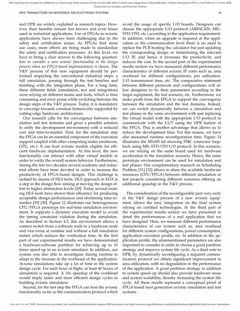
0018-9251 (c) 2017 IEEE. Personal use is permitted, but republication/redistribution requires IEEE permission. See http://www.ieee.org/publications_standards/publications/rights/index.html for more information.
This article has been accepted for publication in a future issue of this journal, but has not been fully edited. Content may change prior to final publication. Citation information: DOI 10.1109/TAES.2017.2733858, IEEETransactions on Aerospace and Electronic Systems
IEEE TRANSACTIONS ON AEROSPACE AND ELECTRONIC SYSTEMS 16
and DPR are widely exploited as research topics. How-ever, their benefits remain less known and even lesserused in industrial applications. Use of FPGAs in avionicapplications have always been challenging due to thesafety and certification issues. As FPGAs find moreuse cases, more efforts are being made to standardizethe safety and certification processes. At this level, wehave to bring a clear answer to the following question:how to consider a new avionic functionality in the designprocess when an FPGA-based implementation is chosen. TheV&V process of this new equipment should be per-formed respecting the conventional industrial steps: afull simulation, passing through the test benches andfinishing with the integration phase. For a long time,these different fields (simulation, test and integration)were relying on different teams and tools, which is timeconsuming and error prone while switching between thedesign steps of the V&V process. Today, it is mandatoryto converge towards common frameworks supported bycutting-edge hardware architectures.
Our research calls for the convergence between sim-ulation and test domains and gives a possible solutionto unify the development environment with a reducedcost and time-to-market. First, for the simulation stepthe FPGA can be an essential component of the executionsupport coupled with other computing nodes (multicore,GPU, etc.). It can host avionic models eligible for effi-cient hardware implementation. At this level, the newfunctionality can interact with other virtual models inorder to verify the overall system behavior. Furthermore,during the last two decades several academic and indus-trial efforts have been devoted in order to increase theproductivity of FPGA-based designs. This challenge istackled by means of HLS tools. HLS approach in EDA isa step in the design flow aiming at moving the design ef-fort to higher abstraction levels [29]. Today several exist-ing HLS tools have shown their efficiency for producingacceptable design performances and shortening time-to-market [29] [30]. Figure 12 illustrates our heterogeneousCPU/FPGA prototype for real-time simulation environ-ment. It supports a dynamic execution model to avoidthe timing constraint violation during the simulation.As described in Section 4.2, this environment allows acontext switch from a software node to a hardware nodeand vice-versa at runtime and without a full simulationrestart which reduces the verification time. In the firstpart of our experimental results we have demonstrateda hardware-software partition for achieving up to 10times speed up in an avionic simulator. In addition, oursystem was also able to reconfigure during runtime toadapt to the increase in the workload of the application.Avionic simulations take up a lot of time in the systemdesign cycle. For each hour of flight, at least 40 hours ofsimulation is required. A 10x speedup of the workloadwould imply faster and more efficient design cycles inbuilding avionic simulation.
Second, for the test step the FPGA can host the avionicfunctionality as far as the communication protocol which
avoid the usage of specific I/O boards. Designers canchoose the appropriate I/O protocol (ARINC429, MIL-STD-1553, etc.) according to the application requirement.In addition, when an upgrade is required at the appli-cation or the communication level there is no need toreplace the PCB hosting the calculator but just updatingthe corresponding design or instantiating the relevantI/O IP, and hence it increases the productivity andreduces the cost. In the second part of the experimentalresults section we have measured different performancecharacteristics of different avionic IP cores such as, areaoverhead for different configurations, pin utilization,I/O transmission time, etc. The comparative statementbetween different protocols and configurations will al-low designers to fix their parameters according to thetarget equipment, the test scenario, etc. Furthermore, wemake profit from the FPGA to support the convergencebetween the simulation and the test domains. Indeed,we can switch dynamically between a simulation andtest phases in the same environment with just replacingthe virtual model with the appropriate I/O protocol tocommunicate with the UUT using the DPR feature ofthe FPGA. This is another advantage that allows us toreduce the development time. For this reason, we havealso measured runtime reconfiguration time. Figure 14illustrates the ML605 kit showing FMC connector loop-back using MIL-STD-1553 I/O protocol. In this scenario,we are relying on the same board used for hardwareacceleration in the simulation scenario. Hence, the sameprototype environment can be used for simulation andtest phases. Our complementary research on SchedulingProblem [31] [32] allows to share the available hardwareresources (CPU/FPGA) between different simulation ortest projects considering different scenarios offering anadditional speedup in the V&V process.
The consideration of the reconfigurable part very earlyin the V&V design process of a new avionic equip-ment allows the easy integration on the final systemrelying on certified technologies. In the third part ofthe experimental results section we have presented indetail the performances of a real application that wehave designed. Here, we measure different performancecharacteristics of our system such as, area overheadfor different system configurations, power consumption,application execution profile, etc. In addition to the ap-plication profile, the aforementioned parameters are alsoimportant to consider in order to choose a good partitionstrategy and improve system life cycle. As a final note toDPR, by dynamically reconfiguring a required commu-nication protocol we obtain significant improvement inarea utilization, with no degradation in the performanceof the application. A good partition strategy in additionto system speed-up should also provide hardware reuseand system scalability, thereby increasing the system lifecycle. All these results represent a conceptual proof ofFPGA-based next generation avionic simulation and testsystems.

0018-9251 (c) 2017 IEEE. Personal use is permitted, but republication/redistribution requires IEEE permission. See http://www.ieee.org/publications_standards/publications/rights/index.html for more information.
This article has been accepted for publication in a future issue of this journal, but has not been fully edited. Content may change prior to final publication. Citation information: DOI 10.1109/TAES.2017.2733858, IEEETransactions on Aerospace and Electronic Systems
IEEE TRANSACTIONS ON AEROSPACE AND ELECTRONIC SYSTEMS 17
9 CONCLUSION
In this paper, we have presented an FPGA-centric designprocess for avionic systems. We have redefined the roleof the FPGA in the different design steps namely thesimulation, the test, and the integration phases. In theproposed process, a particular attention has been givento the smooth transition between the different steps re-lying on the same technology which yields to a reduceddesign cost and time-to-market. The main criteria of re-configurable circuits in terms of performance, flexibilityand dynamicity have been exploited to define versatileavionic systems respecting several design constraints(real-time, area utilization, etc.). This research workaddressed also the challenge of convergence betweenthe simulation and test domains by proposing an FMCstandard-based communication system. The pertinenceof experimental results presents a concept proof of theproposed design process. Future works will deal firstwith the scalability of the system in term of numberof computation nodes in order to cover very complexavionic systems or system-of-systems. Second, we willfocus on the certification of the proposed concepts thatshould be used in the next generation of avionic systems.
ACKNOWLEDGMENT
The authors would like to thank the ANRT (French Na-tional Association of Research and Technology). Indeed,this work was partially funded by the ANRT in the frameof two CIFRE doctoral research grants. The first doctoralgrant was attributed to George Afonso in collaborationwith Airbus Group and the second grant was relatedto the PhD of Venkatasubramanian Viswanathan in col-laboration with Nolam Embedded Systems. In addition,authors would like to thank industrial partners for theirfruitful collaboration in particular Benjamin Nakacheand Maurice Nakache.
REFERENCES
[1] G. Afonso, N. Damiani, N. Belanger, R. B. Atitallah,and M. Rubio, “Hybrid and multicore optimizedarchitectures for test and simulation systems,” inProceedings of the 6th International ICST Conference onSimulation Tools and Techniques, ser. SimuTools ’13,Cannes, French Riviera, 2013.
[2] G. Afonso, R. Ben Atitallah, N. Belanger, M. Rubio,S. Stilkerich, and J. Dekeyser, “Toward generic andadaptive avionic test systems,” in Adaptive Hardwareand Systems (AHS), 2011 NASA/ESA Conference on,June 2011, pp. 287–294.
[3] G. Afonso, R. Ben Atitallah, A. Loyer, J. Dekeyser,N. Belanger, and M. Rubio, “A prototyping en-vironment for high performance reconfigurablecomputing,” in Reconfigurable Communication-centricSystems-on-Chip (ReCoSoC), 2011 6th InternationalWorkshop on, June 2011, pp. 1–8.
[4] V. Viswanathan, R. Ben Atitallah, J.-L. Dekeyser,B. Nakache, and M. Nakache, “Dynamic reconfigu-ration of modular i/o ip cores for avionic applica-tions,” in Reconfigurable Computing and FPGAs (Re-ConFig), 2012 International Conference on, Dec 2012,pp. 1–6.
[5] W. H. Zheng, N. Marzwell, and S. Chau, “In-systempartial run-time reconfiguration for fault recoveryapplications on spacecrafts,” in Systems, Man andCybernetics, 2005 IEEE International Conference on,vol. 4, 2005, pp. 3952–3957 Vol. 4.
[6] B. Osterloh, H. Michalik, S. Habinc, and B. Fiethe,“Dynamic partial reconfiguration in space applica-tions,” in Adaptive Hardware and Systems, 2009. AHS2009. NASA/ESA Conference on, 2009.
[7] L. A. Cardona, J. Agrawal, Y. Guo, J. Oliver, andC. Ferrer, “Performance-area improvement by par-tial reconfiguration for an aerospace remote sensingapplication,” in Reconfigurable Computing and FPGAs(ReConFig), 2011 International Conference on, 2011.
[8] L. Sterpone, F. Margaglia, M. Koester, J. Hagemeyer,and M. Porrmann, “Analysis of seu effects in par-tially reconfigurable sopcs,” in Adaptive Hardwareand Systems (AHS), 2011 NASA/ESA Conference on,2011.
[9] S. J. Lu, P. Siqueira, V. Vijayendra, H. Chan-drikakutty, and R. Tessier, “Real-time differentialsignal phase estimation for space-based systemsusing fpgas,” IEEE Transactions on Aerospace andElectronic Systems, vol. 49, no. 2, pp. 1192–1209,APRIL 2013.
[10] P. M. Nair and S. Ray, “Wireless data acquisitionsystem with signal processing and control moduleswithin field programmable gate array (fpga),” inElectrical, Electronics, Signals, Communication and Op-timization (EESCO), 2015 International Conference on,Jan 2015, pp. 1–6.
[11] M. Lanuzza, P. Zicari, F. Frustaci, S. Perri, andP. Corsonello, “Exploiting self-reconfiguration ca-pability to improve sram-based fpga robustness inspace and avionics applications,” ACM Trans. Re-configurable Technol. Syst., vol. 4, no. 1, dec 2010.
[12] L. A. Tambara, J. Tarrillo, F. L. Kastensmidt, andL. Sterpone, FPGAs and Parallel Architectures forAerospace Applications: Soft Errors and Fault-TolerantDesign. Cham: Springer International Publishing,2016, ch. Fault-Tolerant Manager Core for DynamicPartial Reconfiguration in FPGAs, pp. 121–133.
[13] F. Cloute, J.-N. Contensou, D. Esteve, P. Pampagnin,P. Pons, and Y. Favard, “Hardware/software co-design of an avionics communication protocol in-terface system: an industrial case study,” in Hard-ware/Software Codesign, 1999. (CODES ’99) Proceed-ings of the Seventh International Workshop on, 1999.
[14] R. Bauer, “Embedded synthetic instruments for o-level test: Modular io and fpga technology provideincreased flexibility and decreased cost of test,” inIEEE AUTOTESTCON, 2015, Nov 2015, pp. 284–287.

0018-9251 (c) 2017 IEEE. Personal use is permitted, but republication/redistribution requires IEEE permission. See http://www.ieee.org/publications_standards/publications/rights/index.html for more information.
This article has been accepted for publication in a future issue of this journal, but has not been fully edited. Content may change prior to final publication. Citation information: DOI 10.1109/TAES.2017.2733858, IEEETransactions on Aerospace and Electronic Systems
IEEE TRANSACTIONS ON AEROSPACE AND ELECTRONIC SYSTEMS 18
[15] N. Belanger and J.-P. Lebailly, “Promoting avionictest systems as productivity enablers,” in The fifthInternational Conference on Systems, Les menuires,France, 2010.
[16] N. Belanger, J. Bovier, J.-F. Gilot, J.-P. Lebailly, andM. Rubio, “Multi-Core computers and PCI ExpressThe future of data acquisition and control systems,”in ETTC International Conference, Toulouse, France,2009.
[17] N. Belanger, N. Favarcq, and Y. Fusero, “An openreal time test system approach,” in IEEE Interna-tional Confererence on Advances in System Testing andValidation Lifecycle, Porto, Portugal, Sep. 2009.
[18] H. Plankl, “Embedded solutions for developmenttests, component tests and system integration in thetest centre,” in Aerospace Testing, Munich, Germany,2009.
[19] S. H. VanderLeest and D. White, “Mpsoc hyper-visor: The safe and secure future of avionics,” inDigital Avionics Systems Conference (DASC), 2015IEEE/AIAA 34th, Sept 2015, pp. 6B5–1–6B5–14.
[20] C. Insaurralde, “Reconfigurable computer archi-tectures for dynamically adaptable avionics sys-tems,” IEEE Aerospace and Electronic Systems Mag-azine, vol. 30, no. 9, pp. 46–53, Sept 2015.
[21] G. Afonso, W. Godard, R. Ben Atitallah, and J.-L.Dekeyser, “Test and simulation system,” World In-tellectual Property Organization, Patent, no. Number:WO 2015/097105 A1, July 2015.
[22] S. Asano, T. Maruyama, and Y. Yamaguchi, “Per-formance Comparison of FPGA, GPU AND CPU inImage Processing,” in 19th IEEE International Con-ference on Field Programmable Logic and Applications,FPL, Prague, Czech Republic, Aug. 2009.
[23] O. Souissi, R. Ben Atitallah, A. Artiba, and S. E.Elmaghraby, “Optimization of run-time mappingon heterogeneous cpu/fpga architectures,” in 9thInternational Conference of Modeling, Optimization andSimulation - MOSIM12, Bordeaux, France, 2012.
[24] VectorFabrics: Pareon, “Analyze your sequential Ccode to create an optimized parallel implementa-tion,” 2013, http://www.vectorfabrics.com/.
[25] P. Coussy, C. Chavet, P. Bomel, D. Heller, E. Senn,and E. Martin, GAUT: A High-Level Synthesis Tool forDSP Applications, P. Coussy and A. Morawiec, Eds.Springer Netherlands, 2008. [Online]. Available:http://dx.doi.org/10.1007/978-1-4020-8588-8 9
[26] J. R. Villarreal, A. Park, W. A. Najjar, and R. Hal-stead, “Designing modular hardware accelerators inc with roccc 2.0,” in 18th IEEE Annual InternationalSymposium on Field-Programmable Custom Comput-ing Machines, FCCM 2010, Charlotte, North Carolina,USA, 2-4 May 2010, 2010, pp. 127–134.
[27] A. Jacobs, G. Cieslewski, A. D. George, A. Gordon-Ross, and H. Lam, “Reconfigurable fault tolerance:A comprehensive framework for reliable and adap-tive fpga-based space computing,” ACM Trans. Re-configurable Technol. Syst., vol. 5, no. 4, pp. 21:1–
21:30, Dec. 2012.[28] R. B. Atitallah, E. Senn, D. Chillet, M. Lanoe,
and D. Blouin, “An efficient framework forpower-aware design of heterogeneous mpsoc,”IEEE Trans. Industrial Informatics, vol. 9,no. 1, pp. 487–501, 2013. [Online]. Available:http://dx.doi.org/10.1109/TII.2012.2198657
[29] R. Nane, V. M. Sima, C. Pilato, J. Choi, B. Fort,A. Canis, Y. T. Chen, H. Hsiao, S. Brown, F. Ferrandi,J. Anderson, and K. Bertels, “A Survey and Evalu-ation of FPGA High-Level Synthesis Tools,” IEEETransactions on Computer-Aided Design of IntegratedCircuits and Systems, vol. PP, no. 99, pp. 1–1, 2016.
[30] W. Meeus, K. Van Beeck, T. Goedeme,J. Meel, and D. Stroobandt, “An Overviewof Today’s High-Level Synthesis Tools,” DesignAutomation for Embedded Systems, vol. 16,no. 3, pp. 31–51, 2012. [Online]. Available:http://dx.doi.org/10.1007/s10617-012-9096-8
[31] A. Ait El Cadi, R. Ben Atitallah, S. Hanafi,N. Mladenovic, and A. Artiba, “New mipmodel for multiprocessor scheduling prob-lem with communication delays,” OptimizationLetters, pp. 1–17, 2014. [Online]. Available:http://dx.doi.org/10.1007/s11590-014-0802-2
[32] A. Ait El Cadi, O. Souissi, R. Ben Atitallah, N. Be-langer, and A. Artiba, “Mathematical programmingmodels for scheduling in a cpu/fpga architecturewith heterogeneous communication delays,” Journalof Intelligent Manufacturing, pp. 1–12, 2015. [Online].Available: http://dx.doi.org/10.1007/s10845-015-1075-z
Rabie Ben Atitallah received his PhD degreein Computer Science from the University of Lille1 in March 2008. In September 2009, RabieBen Atitallah obtained a full-time position as anAssociate Professor in Computer Science at theUVHC and a member of LAMIH laboratory (UMRCNRS/UVHC 8201) within the DIM (Decision,Interaction, and Mobility) team. In December2014, he received the Habilitation degree inComputer Science from the UVHC. In addition,he had the status of Associated Researcher at
INRIA Lille Nord Europe within the DaRT and DreamPal team-projectsuntil the end of 2016. Currently, Rabie Ben Atitallah is the scientificanimator of the theme OPTIMOB (stands for Optimization and Mobility).Rabie Ben Atitallah was the task manager of INRIA Lille in the frame ofthe ANR OpenPeople (2009 - 2013). Also, he was managing severalindustrial collaborations (more then 10 projects) with Airbus GroupInnovation, Airbus Helicopters, Navya, Nolam Embedded Systems, etc.He co-authored more than 80 publications (patents, journals, and in-ternational conferences). Due to his significant scientific contributions,he holds the scientific award of excellence and he is nominated asa member of the National University Committee (CNU) in computerscience. His research domain covers embedded system design forintelligent transportation, reconfigurable computing, low power-awaredesign, high level synthesis tools and design space exploration.
0018-9251 (c) 2017 IEEE. Personal use is permitted, but republication/redistribution requires IEEE permission. See http://www.ieee.org/publications_standards/publications/rights/index.html for more information.
This article has been accepted for publication in a future issue of this journal, but has not been fully edited. Content may change prior to final publication. Citation information: DOI 10.1109/TAES.2017.2733858, IEEETransactions on Aerospace and Electronic Systems
IEEE TRANSACTIONS ON AEROSPACE AND ELECTRONIC SYSTEMS 19
Venkatasubramanian Viswanathan Venkata-subramanian VISWANATHAN received his MScin Computer Engineering specializing in GeneralPurpose and High Performance Systems fromTU Delft, Netherlands in October 2011. He thenjoined the INRIA Lille Lab as a Research En-gineer in the Hommmade project. He then pur-sued his (CIFRE/Industrial) PhD under the su-pervision of Jean-Luc Dekeyser and Rabie BenAtitallah in collaboration with Nolam EmbeddedSystems. During this time, he has co-authored
5 international publications. He received his PhD in October 2015. Heis currently working as a consultant with the NOKIA X-HAUL R&DFPGA labs designing complex System on Chips (SoC) on FPGAs for5G point-to-point radio communications. His research interests includeembedded system design, reconfigurable systems design, high-speeddigital design, ASIC/SoC design, runtime reconfigurable systems andelectronic design automation (EDA)
Nicolas Belanger Discovering particular physi-cal aptitude in his early years, Nicolas Belangerbecame a high level athlete totally attracted by acareer in sport. After two years playing basket-ball in semi-professional teams, he turned backto university studies and passed his PhD degreein Artificial Intelligence at the University of Mar-seille under the direction of Eugene Chouraqui.Integrating the General Motors group by its sub-sidiary EDS, he then spent 9 years in the de-manding ICT services world as Project Director
or as Head of HiTech Consulting Agency. Jumping into the industrialworld in 2007, Nicolas integrated Airbus Helicopters where he is beingin charge of the ICT Embedded Systems at the Innovation Department.Defining himself as a fresh minded person, Nicolas is a science andtechnology bulimic. Nicolas has developed an expertise in the field ofIntelligent Algorithms to solve in flight complex situations. This specialtyrequires in-depth knowledge in 3D Motion Planning, optimization un-der constraints, knowledge engineering, numerical analysis, differentialgeometry, HW/SW co-designed embedded architectures and intelligentsensors. On top of that Nicolas has a personal passion for mathematicalapproximation theory and he recently discovered a method to solvethe Runge phenomenon with high degree polynomials relying on eq-uispaced nodes which he will present in next mathematics conferences.
Jean-Luc Dekeyser Jean-Luc Dekeyser re-ceived his PhD degree in computer science fromthe university of Lille in 1986, he was a fellowshipat CERN Geneva. After a few years at the Su-percomputing Computation Research Institutein Florida State University, where he workedon high performance computing for Mont-Carlomethods in High Energy Physics, he joined in1988 the University of Lille in France as an assis-tant professor. There he worked on data parallelparadigm and vector processing. He created a
research group working on High Performance Computing in the CNRSlab in Lille. He is currently Professor in computer science at Universityof Lille. He was heading the DaRT Inria project between 2004 and 2012.His research interests include embedded systems, System on Chip co-design, synthesis and simulation, performance evaluation, high perfor-mance computing, model driven engineering, dynamic reconfiguration,and 3D Chip.