ieee photonics technology letters, vol. 27, no. 6, … kuchta_71g_ptl2015.pdf · ieee photonics...
TRANSCRIPT

IEEE PHOTONICS TECHNOLOGY LETTERS, VOL. 27, NO. 6, MARCH 15, 2015 577
A 71-Gb/s NRZ Modulated 850-nmVCSEL-Based Optical Link
Daniel M. Kuchta, Senior Member, IEEE, Alexander V. Rylyakov, Fuad E. Doany,Clint L. Schow, Senior Member, IEEE, Jonathan E. Proesel, Member, IEEE,
Christian W. Baks, Petter Westbergh, Johan S. Gustavsson,and Anders Larsson, Fellow, IEEE
Abstract— We report error free (BER < 10−12) operation ofa directly non-return-to-zero modulated 850-nm vertical cavitysurface-emitting laser (VCSEL) link operating to 71 Gb/s. Thisis the highest error free modulation rate for a directly modu-lated laser of any type. The optical link consists of a 130-nmBiCMOS driver IC with two-tap feed-forward equalization,a wide bandwidth 850-nm VCSEL, a surface illuminated GaAsPIN photodiode, and a 130-nm BiCMOS receiver IC.
Index Terms— High-speed modulation, optical interconnects,semiconductor lasers, vertical cavity surface-emitting laser.
I. INTRODUCTION
SERIAL data rates continue to increase for the major datacommunications standards: Ethernet, Infiniband, Fibre
Channel and PCI Express. While still under discussion, theInfiniband HDR serial rate could be 51.5625 Gb/s. Today,direct Non-Return-to-Zero (NRZ) modulation of 850 nmVCSELs and multimode fiber make up the vast majority of thevolume of data communication links in the field. It is worth-while exploring the limits of this technology. For directly mod-ulated edge emitting DFB lasers, the highest reported data rateis 56.1 Gb/s [1], and for directly NRZ modulated VCSELs it is64 Gb/s [2]. In this letter we report error free (BER < 10−12),direct NRZ modulation of an 850 nm VCSEL-based linkup to 71 Gb/s. This is the highest reported error free directmodulation rate for any laser to date.
II. OPTICAL LINK COMPONENTS
The optical link consists of a transmitter subassembly(driver IC and VCSEL) connected to a receiver subassem-bly (receiver IC and photodiode) through 7 m of standardOM3 50/125 μm multimode fiber. The following subsectionsdescribe each of the sub-components in detail.
Manuscript received November 5, 2014; revised December 9, 2014;accepted December 18, 2014. Date of publication January 6, 2015; date ofcurrent version February 19, 2015. This work was supported in part by theSwedish Foundation for Strategic Research.
D. M. Kuchta, A. V. Rylyakov, F. E. Doany, C. L. Schow, J. E. Proesel,and C. W. Baks are with the IBM Thomas J. Watson Research Center,Yorktown Heights, NY 10598 USA (e-mail: [email protected]; [email protected]; [email protected]; [email protected]; [email protected]; [email protected]).
P. Westbergh, J. S. Gustavsson, and A. Larsson are with the PhotonicsLaboratory, Department of Microtechnology and Nanoscience, ChalmersUniversity of Technology, Gothenburg 412 58, Sweden (e-mail:[email protected]; [email protected]; [email protected]).
Color versions of one or more of the figures in this letter are availableonline at http://ieeexplore.ieee.org.
Digital Object Identifier 10.1109/LPT.2014.2385671
Fig. 1. Photograph of transmitter showing driver IC, VCSELs, decouplingcapacitors and printed circuit board traces.
A. Transmitter Subassembly
Fig. 1 shows a picture of the center of the transmittersubassembly on a printed circuit board (PCB). In the centeris the driver IC which is surrounded on two sides by powersupply decoupling capacitors. The decoupling capacitors usedare 560 pF (0202 size) although high speed operation is notparticularly sensitive to this value. The other two sides are forthe high speed signal input and the connection to the VCSELs.The 1 mm2 driver IC is implemented in 130 nm BiCMOS andincorporates 2-tap linear Feed Forward Equalization (FFE) inthe differential output stage. It is similar to the one describedin [4] but with a shorter delay in the FFE path. All connectionsto the driver chip are through short (∼300–500 μm) wire-bonds. The high speed connections to PCB are through surfacemounted vertical SMP connectors located 4.7 mm away fromthe driver chip through single-ended 50 � transmission lineson the top surface. The impedance of the driver IC differentialinput is 100 �. Careful design went into the PCB footprint forthe SMP connectors to minimize the discontinuity. Betweenthe SMP connectors and the driver IC are 100 nF (0201 size)dc blocking capacitors. The VCSELs are mounted as close aspossible to the driver IC in a common anode configuration.This configuration allows for separate optimization of theVCSEL and circuit supplies and lowers the power dissipation.Because the VCSEL is cathode driven, it is very importantto make the anode power supply as close to an ideal acground as possible. To this extent, two capacitors are triplewirebonded in parallel to the PCB, a 1200 pF (0202 size) anda 10 nF (0202 size). Only single wirebonds are used for
1041-1135 © 2015 IEEE. Personal use is permitted, but republication/redistribution requires IEEE permission.See http://www.ieee.org/publications_standards/publications/rights/index.html for more information.

578 IEEE PHOTONICS TECHNOLOGY LETTERS, VOL. 27, NO. 6, MARCH 15, 2015
Fig. 2. Simulation of driver IC output current at 71 Gb/s showing the feedforward equalization characteristics.
connections to the VCSEL due to the small pad sizes. Alsoimportant for cathode driving is to minimize the VCSELparasitic capacitance to ground which goes contrary to cus-tomary anode driving. To reduce this parasitic capacitance, theVCSELs are mounted on an AlN submount which has half itsthickness removed beneath the VCSELs to create an air gapbetween the VCSELs and the PCB.
For this very high speed operation, most of the driver chipsupply voltages were set for 4 V. The total power consumptionof the transmitter was 950 mW (13.4pJ/bit) including theVCSEL which is biased at 8.2 mA. Fig. 2 shows a simulationof the output current of the driver IC at 71 Gb/s. Substantialover- and under-shoot can be seen in the driving waveformwhich originates from the FFE characteristics.
B. VCSEL
The VCSEL used in the experiments is the same as wasused for the 64 Gb/s measurements in [2]. In the VCSELstructure (provided by IQE Europe), five strained InGaAsquantum wells are contained within a short 0.5-λ cavity forhigh differential gain at 850 nm. Lateral optical and currentconfinement is provided by two 5 μm diameter primaryoxide apertures, while four larger diameter secondary oxideapertures are used to reduce the parasitic capacitance. Thethickness of the topmost GaAs layer was tuned to optimizethe photon lifetime for a large modulation bandwidth anda flat modulation response. At 8.2 mA, the output poweris 5.0 mW and the 3 dB modulation bandwidth is ∼26 GHz.The D- and K -factors [3] for the VCSEL are 11.5 GHz/mA1/2
and 0.14 ns respectively. Fig. 3 shows the L-I-V curves andan optical spectrum for this VCSEL.
C. Receiver Subassembly and Photodiode
Fig. 4 shows a photograph of the receiver subassemblywith the receiver IC located in the center. The PCB layoutis the same as for the transmitter. The receiver IC design,described in [4], is similar to the transmitter but contains atransimpedance amplifier with a 480 � feedback resistor atthe input stage. A GaAs PIN photodiode (PD) is placed asclose as possible to the receiver IC to shorten the wirebondlength. The photodiode is mounted on an Alumina submountto reduce its capacitance to ground and to elevate it slightly
Fig. 3. Room temperature L-I-V characteristics of the VCSEL. Dot showsbias point for 71 Gb/s operation Inset: optical spectrum at 8.5 mA.
Fig. 4. Photograph of receiver showing receiver IC, photodiode, decouplingcapacitors and printed circuit board traces.
above the IC for wirebonding purposes. The photodiode is dcbiased through the IC using a pair of 2 k� resistors, one ateach terminal. The high speed signal is ac coupled on chip tothe the TIA input. This receiver is identical to the one used forthe 64 Gb/s measurements in [2] but with two importantchanges: the photodiode diameter was reduced from 21 μmto 12 μm and the photodiode intrinsic layer thickness wasreduced from 1.6 μm to 1.0 μm. Accompanying these changeswas a drop in bias voltage from 7.0 to 5.7 V. The propertiesof the two photodiodes have been reported in detail in [5].The change to a smaller area, thinner photodiode lowered thecapacitance slightly from 73 to 61 fF, reduced the responsivityslightly from 0.55 to 0.48 A/W and increased the bandwidthfrom 22 to >30 GHz. The increase in bandwidth was theenabling factor to move from 64 to 71 Gb/s. Most of thereceiver supply voltages are 4 V and the power consumptionis 860 mW with a single ended output amplitude of 200 mV.In experiments with the 21 μm photodiode, a lensed 50 μmfiber probe can be used with very high coupling efficiency.For coupling to the 12 μm photodiode, an aspheric lens withan 11 mm focal length (Thorlabs F220FC-B) was used tocollimate the light and another aspheric lens with a 2.8 mm
KUCHTA et al.: 71-Gb/s NRZ MODULATED 850-nm VCSEL-BASED OPTICAL LINK 579
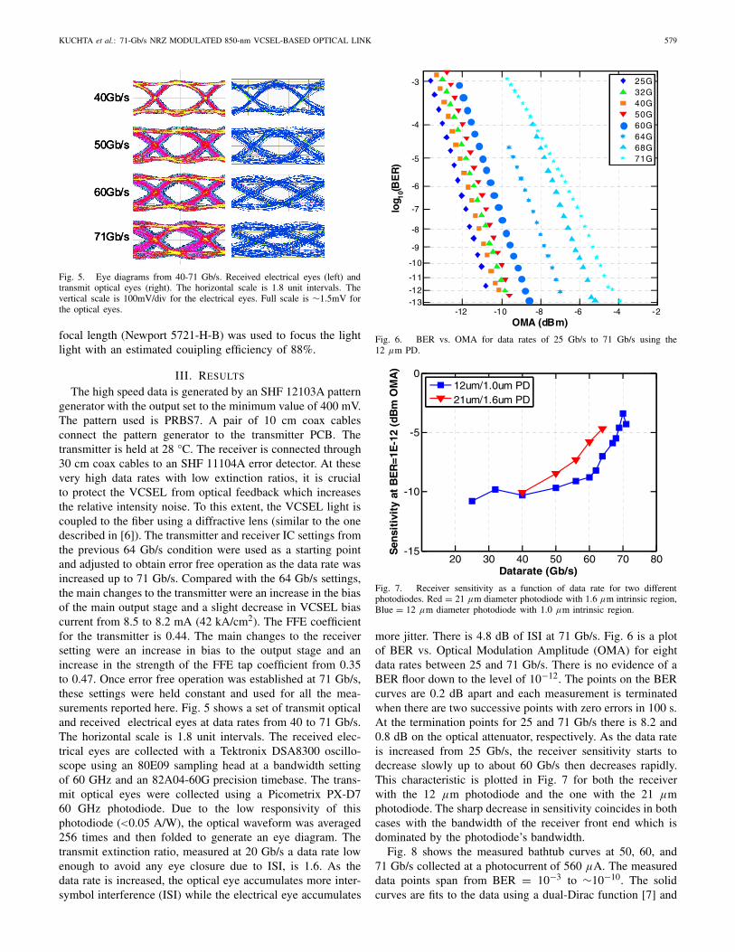
Fig. 5. Eye diagrams from 40-71 Gb/s. Received electrical eyes (left) andtransmit optical eyes (right). The horizontal scale is 1.8 unit intervals. Thevertical scale is 100mV/div for the electrical eyes. Full scale is ∼1.5mV forthe optical eyes.
focal length (Newport 5721-H-B) was used to focus the lightlight with an estimated couipling efficiency of 88%.
III. RESULTS
The high speed data is generated by an SHF 12103A patterngenerator with the output set to the minimum value of 400 mV.The pattern used is PRBS7. A pair of 10 cm coax cablesconnect the pattern generator to the transmitter PCB. Thetransmitter is held at 28 °C. The receiver is connected through30 cm coax cables to an SHF 11104A error detector. At thesevery high data rates with low extinction ratios, it is crucialto protect the VCSEL from optical feedback which increasesthe relative intensity noise. To this extent, the VCSEL light iscoupled to the fiber using a diffractive lens (similar to the onedescribed in [6]). The transmitter and receiver IC settings fromthe previous 64 Gb/s condition were used as a starting pointand adjusted to obtain error free operation as the data rate wasincreased up to 71 Gb/s. Compared with the 64 Gb/s settings,the main changes to the transmitter were an increase in the biasof the main output stage and a slight decrease in VCSEL biascurrent from 8.5 to 8.2 mA (42 kA/cm2). The FFE coefficientfor the transmitter is 0.44. The main changes to the receiversetting were an increase in bias to the output stage and anincrease in the strength of the FFE tap coefficient from 0.35to 0.47. Once error free operation was established at 71 Gb/s,these settings were held constant and used for all the mea-surements reported here. Fig. 5 shows a set of transmit opticaland received electrical eyes at data rates from 40 to 71 Gb/s.The horizontal scale is 1.8 unit intervals. The received elec-trical eyes are collected with a Tektronix DSA8300 oscillo-scope using an 80E09 sampling head at a bandwidth settingof 60 GHz and an 82A04-60G precision timebase. The trans-mit optical eyes were collected using a Picometrix PX-D760 GHz photodiode. Due to the low responsivity of thisphotodiode (<0.05 A/W), the optical waveform was averaged256 times and then folded to generate an eye diagram. Thetransmit extinction ratio, measured at 20 Gb/s a data rate lowenough to avoid any eye closure due to ISI, is 1.6. As thedata rate is increased, the optical eye accumulates more inter-symbol interference (ISI) while the electrical eye accumulates
Fig. 6. BER vs. OMA for data rates of 25 Gb/s to 71 Gb/s using the12 μm PD.
Fig. 7. Receiver sensitivity as a function of data rate for two differentphotodiodes. Red = 21 μm diameter photodiode with 1.6 μm intrinsic region,Blue = 12 μm diameter photodiode with 1.0 μm intrinsic region.
more jitter. There is 4.8 dB of ISI at 71 Gb/s. Fig. 6 is a plotof BER vs. Optical Modulation Amplitude (OMA) for eightdata rates between 25 and 71 Gb/s. There is no evidence of aBER floor down to the level of 10−12. The points on the BERcurves are 0.2 dB apart and each measurement is terminatedwhen there are two successive points with zero errors in 100 s.At the termination points for 25 and 71 Gb/s there is 8.2 and0.8 dB on the optical attenuator, respectively. As the data rateis increased from 25 Gb/s, the receiver sensitivity starts todecrease slowly up to about 60 Gb/s then decreases rapidly.This characteristic is plotted in Fig. 7 for both the receiverwith the 12 μm photodiode and the one with the 21 μmphotodiode. The sharp decrease in sensitivity coincides in bothcases with the bandwidth of the receiver front end which isdominated by the photodiode’s bandwidth.
Fig. 8 shows the measured bathtub curves at 50, 60, and71 Gb/s collected at a photocurrent of 560 μA. The measureddata points span from BER = 10−3 to ∼10−10. The solidcurves are fits to the data using a dual-Dirac function [7] and

580 IEEE PHOTONICS TECHNOLOGY LETTERS, VOL. 27, NO. 6, MARCH 15, 2015
Fig. 8. Bathtub curves for 50, 60 and 71 Gb/s (outer to inner).
Fig. 9. Eye opening at BER = 10−12 as a function of data rate from25 to 71 Gb/s.
the points at BER = 10−12 are from the fit. At 50 Gb/s the eyeopening (EO) at BER = 10−12 is 0.49 UI, the deterministicjitter (DJ) is 4.7 ps and the random jitter (RJ) is 5.4 ps.At 71 Gb/s there is almost no timing margin withEO = 0.08 UI, DJ = 4.2 ps and RJ = 8.7 ps. The extractedDJ at 71 Gb/s is lower than that at 50 Gb/s and lower thanthe 6.9 ps observed in the optical eye. This can be partiallyexplained by the dual-Dirac fit to the data but mostly due tothe settings of the receiver FFE which were tuned to givethe best eye opening at 71 Gb/s. The large increase in RJ ispartially attributed to the error detector as the optical eyes donot exhibit this much increase in jitter.
The evolution of the EO with data rate is plotted in Fig. 9for 25 to 71 Gb/s and exhibits an almost parabolic shape.At 25 Gb/s, the EO is as large as 0.68 UI. Continuingthe trend downward, the EO appears to go to zero around73 Gb/s, a data rate beyond where the error detector currentlyoperates.
IV. DISCUSSION AND CONCLUSION
We have reported on the details and characteristics of amultimode fiber link that is able to operate error free up
to 71 Gb/s using an 850 nm VCSEL as the light source anda surface illuminated GaAs PIN photodiode as the detector.This is the highest reported error free modulation speed for adirectly modulated NRZ optical link to date. As serial speedscontinue to increase it is worthwhile to see if 100 Gb/s NRZmodulation could be attainable. From a circuits point of view,100 Gb/s NRZ signaling has already been demonstrated inmultiple technologies for more than 10 years now [8]. Progressin high speed VCSELs has been rather rapid with at least threeseparate institutions reaching the 50 Gb/s level in just the pasttwo years [9]–[11]. Part of this progress can be attributed tohigh speed test equipment that is now available commerciallywhile another part can be traced to commercial interest inhigh speed lasers. To reach 100 Gb/s, both the VCSEL andphotodiode would need about a 30-40% increase in bandwidthto the ∼40 GHz level. Photodiodes have been shown toachieve these bandwidth albeit with a reduction in responsivity.The VCSEL in this experiment has a K -factor of 0.14 nswhich implies an intrinsic damping-limited laser bandwidthof more than 60 GHz but the real limitation is the parasiticbandwidth and thermal saturation. There is also a trade-offbetween modulation bandwidth and the laser damping whichhas to be taken into account [12]. Given the rapid progressand the prospects for reducing parasitics, providing better heatsinking, and the use of equalization techniques, a 100 Gb/sNRZ modulated link seems viable.
REFERENCES
[1] K. Nakahara et al., “56-Gb/s direct modulation in InGaAlAs BH-DFBlasers at 55 °C,” in Proc. Opt. Fiber Commun. Conf. Exhibit. (OFC),Mar. 2014, pp. 1–3.
[2] D. Kuchta et al., “64 Gb/s transmission over 57 m MMF using anNRZ modulated 850 nm VCSEL,” in Proc. Opt. Fiber Commun. Conf.Exhibit. (OFC), Mar. 2014, pp. 1–3.
[3] D. Tauber, G. Wang, R. S. Geels, J. E. Bowers, and L. A. Coldren,“Large and small signal dynamics of vertical cavity surface emittinglasers,” Appl. Phys. Lett., vol. 62, no. 4, pp. 325–327, 1993.
[4] A. V. Rylyakov et al., “A 40-Gb/s, 850-nm, VCSEL-based full opticallink,” in Proc. Nat. Fiber Opt. Eng. Conf. Opt. Fiber Commun. Conf.Expo. (OFC/NFOEC), Mar. 2012, pp. 1–3.
[5] N. Dupuis et al., “Exploring the limits of high-speed receivers formultimode VCSEL-based optical links,” in Proc. Opt. Fiber Commun.Conf. Exhibit. (OFC), Mar. 2014, pp. 1–3.
[6] C. Coleman, Y. C. Chen, X. Wang, H. Welch, and B. TeKolste,“Diffractive optics in a parallel fiber transmitter module,” in DiffractiveOptics and Micro-Optics (OSA Trends in Optics and Photonics), vol. 75,R. Magnusson, Ed. Washington, DC, USA: Optical Society of America,2002, paper DThB4.
[7] B. Ham, “Fibre channel—Methodologies for jitter and signal qual-ity specification—MJSQ,” in Proc. Int. Committee Inf. Technol.Standards (INCITS), pp. 29–38, 2004.
[8] T. Swahn, Y. Baeyens, and M. Meghelli, “ICs for 100-Gb/s serialoperation,” IEEE Microw. Mag., vol. 10, no. 2, pp. 58–67,Apr. 2009.
[9] P. Moser, J. A. Lott, P. Wolf, G. Larisch, H. Li, and D. Bimberg, “Error-free 46 Gbit/s operation of oxide-confined 980 nm VCSELs at 85 °C,”Electron. Lett., vol. 50, no. 19, pp. 1369–1371, Sep. 2014.
[10] P. Westbergh, E. P. Haglund, E. Haglund, R. Safaisini, J. S. Gustavsson,and A. Larsson, “High-speed 850 nm VCSELs operating error freeup to 57 Gbit/s,” Electron. Lett., vol. 49, no. 16, pp. 1021–1023,Aug. 2013.
[11] D. M. Kuchta et al., “A 56.1 Gb/s NRZ modulated 850 nmVCSEL-based optical link,” in Proc. Opt. Fiber Commun. Conf.Expo. Nat. Fiber Opt. Eng. Conf. (OFC/NFOEC), Mar. 2013,pp. 1–3.
[12] E. P. Haglund, P. Westbergh, J. S. Gustavsson, and A. Larsson, “Impactof damping on high-speed large signal VCSEL dynamics,” J. Lightw.Technol., to be published.