ieee journal of solid-state circuits, vol. 45, …ims.unipv.it/firb2006/pub/fanori10a.pdf · 4 ieee...
TRANSCRIPT

This article has been accepted for inclusion in a future issue of this journal. Content is final as presented, with the exception of pagination.
IEEE JOURNAL OF SOLID-STATE CIRCUITS, VOL. 45, NO. 12, DECEMBER 2010 1
Capacitive Degeneration in LC-Tank Oscillator forDCO Fine-Frequency Tuning
Luca Fanori, Student Member, IEEE, Antonio Liscidini, Member, IEEE, and Rinaldo Castello, Fellow, IEEE
Abstract—A digitally controlled oscillator (DCO) that achievesa minimum frequency quantization step of 150 Hz without anydithering is presented. The fine digital tuning is obtained througha capacitive degeneration of a portion of the transistor switchingpair used in a classical LC-tank oscillator. The new tuning cir-cuitry does not appreciably affect the intrinsic oscillator phasenoise and allows to trim the frequency with a programmableresolution for calibration and multi-standard operation. A pro-totype integrated in 65 nm CMOS technology exhibits a phasenoise of 127.5 dBc Hz @ 1 MHz drawing 16 mA from a supplyof 1.8 V, resulting in a FoM of 183 dBc/Hz. The active area is700 m 450 m.
Index Terms—ADPLL, capacitance shrinking, DCO, digitallycontrolled oscillator, fine tuning, GSM, LC-tank oscillator.
I. INTRODUCTION
T HE migration of phase-locked loops (PLL) towards all-digital architectures with a comparable and even better
performance will be made possible by further technology evolu-tion that will allow to achieve an adequate quantization of timeand frequency [1]. In particular, a fine resolution of the time-to-digital converter (TDC) is required to minimize the quantizationnoise introduced in the PLL band, while a tiny frequency dis-cretization of the DCO allows to reduce the noise added far fromthe carrier. Although the technology evolves by itself in the di-rection of these goals, with shorter delay stages and smaller par-asitic capacitances, the target resolutions for wireless applica-tions are still quite challenging to make possible a simple trans-position of analog solutions into digital ones [1]. For example, inthe design of a DCO for GSM applications, the target frequencyresolution of few kHz with respect to a tuning range of severalhundred MHz around the carrier (e.g., 400 MHz in GSM [2])results in unitary capacitive elements of the order of atto-Faradthat cannot be easily integrated [3]. A possible solution is theuse of capacitive divider networks to obtain a reduction of theminimum effective capacitance that can be switched in parallelto the tank [4]. This approach can improve the DCO frequencyresolution but the sensitivity to mismatches and parasites limitsthe robustness of the final design. A more reliable technique pro-posed by Staszewski et al. [2] consists in the dithering of theless significant bits of the DCO frequency control word (like
Manuscript received April 15, 2010; revised August 08, 2010; acceptedAugust 08, 2010. This paper was approved by Guest Editor Kari Halonen.This work was supported by the Italian National Program FIRB, ContractRBIP063L4L.
The authors are with the Dipartimento di Elettronica, Laboratorio di Mi-croelettronica, Università degli Studi di Pavia, 27100 Pavia, Italy, (e-mail: [email protected]; [email protected]; [email protected]).
Digital Object Identifier 10.1109/JSSC.2010.2077190
Fig. 1. Proposed fine-tuning DCO scheme.
in a sigma-delta DAC). This solution reduces considerably theequivalent DCO frequency resolution (from 12 kHz to 30 Hz in[2]) but, as it occurs in any sigma-delta data converter, the quan-tization noise is moved to higher frequencies where the phasenoise specs may be even more challenging. Due to this problem,the frequency of dithering must be very high (e.g., 225 MHz) tosatisfy the emission mask requirements far away from the car-rier [2].
All the solutions presented in literature try to improve theDCO resolution working at the level of the oscillator tank, ei-ther making a custom design of the capacitive element or ex-ploiting some kind of shrinking effect of the elements of theLC resonator [2]–[7]. The idea of this work is to move part ofthe tuning bank from the tank to the sources of the switchingpair of the LC oscillator exploiting an intrinsic shrinking effectpresent in the structure (Fig. 1). The portion of the capacitivearray still in parallel to the tank (named coarse tuning bank) isused to compensate process and temperature variation, while theportion at the source of M1 and M2 (named fine tuning bank)is used for the DCO modulation inside the PLL. As it will beshown, this approach allows an easier design of both coarse andfine tuning banks, avoiding the use of dithering and without in-troducing any degradation in the DCO phase-noise.
The paper is organized as follows: in Section II the fine tuningscheme is introduced, focusing on the main mechanism that pro-duces an equivalent scaled down replica of the fine tuning bankin parallel to the tank (Fig. 1). The impact on phase-noise per-formance is analyzed at the end of Section II and in more detailin the Appendixes. In Section III, the fine-tuning range and itscalibration are discussed while in Section IV the design of a pro-totype in 65 nm CMOS technology tailored to GSM application
0018-9200/$26.00 © 2010 IEEE

This article has been accepted for inclusion in a future issue of this journal. Content is final as presented, with the exception of pagination.
2 IEEE JOURNAL OF SOLID-STATE CIRCUITS, VOL. 45, NO. 12, DECEMBER 2010
is presented. A complete set of experimental measurements car-ried out on the prototype are reported in Section V, together witha comparison with the state of the art.
II. BASIC IDEA
In general, the role of the transistor switching pair in a classicLC tank oscillator is to sustain the oscillations restoring the en-ergy losses that occur in the tank [8]. This operation is com-monly represented as a negative resistance in shunt with the res-onant load that, to a first approximation, does not affect the os-cillator frequency ( ). This frequency is adjusted acting onthe total capacitance present in the tank ( ) so that
(1)
where is the variation in the oscillation frequency causedby a change in the total capacitance of the tank . Afrequency resolution of less than a few ppm (e.g., 1kHz over 3.6 GHz) would require almost the same tank capaci-tance resolution . This corresponds to an exceed-ingly small unitary element in the capacitor tuning bank whenthe total capacitance in the tank is in the order of pico-Farad. Inthis section it will be shown that this problem can be overcomeusing the capacitive degeneration introduced in Fig. 1 that addsa reactive component to the classical negative resistance pro-viding an additional tuning mechanism.
A. DCO Equivalent Circuit
Since the circuit operates in a large signal regime, the struc-ture has been studied using a small signal time variant analysis[9], where the MOS transconductance was averaged over atime interval equal to one period of the oscillation frequency
(high order harmonics were neglected for simplicity).Under these assumptions, the oscillator reported in Fig. 1 can bemodeled by the scheme reported in Fig. 2. In fact, the signal cur-rent that flows into transistor M1-M2 is the same as that flowsinto capacitance and is related to the voltage across the tankwith an inversion of sign due the gate-drain cross-connections.
The effect of on the DCO frequency tuning characteristiccan be estimated evaluating the admittance (indicated inFig. 2 as ) using a series to parallel conversion in thecircuit of Fig. 2. The admittance can be expressed as follows:
(2)
where is the oscillation frequency of the DCO. For(2) can be rewritten as
(3)
where becomes the classical negative conductance whichcompensates tank losses [8], while is equal to the capac-itor shrunk by a factor . As shown in (3)this factor is equal to , where is the quality factor1 of the
1The quality factor is defined only as �����������
Fig. 2. DCO equivalent scheme.
Fig. 3. Real and Imaginary par of admittance � ( �� � , � ��� �, � ��� GHz).
impedance which models the degenerated switching pair givenby
(4)
If the quality factor is reduced, the equivalent capacitanceat the tank diminishes. It will be shown that, although hasto be lower than one to provide a shrinking effect, this doesnot have any adverse effect on phase noise or amplitude of theLO since the impedance in parallel to the tank is negative andrestores DCO losses.
Starting from (2), and have been plotted in Fig. 3versus (assuming and GHz).
shows a monotonic behavior that asymptotically tends towhile is not monotonic and starts to decrease for
. Since the absolute value of the (negative)real part of has to be larger than to sustain the os-cillation, the useful portion of the plot of Fig. 3 corresponds to
greater than (i.e., the minimum value of for which). From the plot of Fig. 3 it can be seen that, for
the set of parameters used, a capacitor pF is reflected inparallel to the tank into an equivalent capacitance fFwith a shrinking factor of about 200. This means that switchingon a capacitor of 5 fF at the sources of M1-M2 produces thesame effect as switching on a capacitor of 25 aF in parallel tothe oscillator tank.

This article has been accepted for inclusion in a future issue of this journal. Content is final as presented, with the exception of pagination.
FANORI et al.: CAPACITIVE DEGENERATION IN LC-TANK OSCILLATOR FOR DCO FINE-FREQUENCY TUNING 3
Fig. 4. DCO fine frequency tuning (� � �� ��).
B. DCO Fine-Frequency Tuning Characteristic
The tuning characteristic of the oscillator as a function of thecapacitance (i.e., ) can be found evaluatingthe resonance frequency of the circuit of Fig. 2 and is given bythe following expression:
(5)
where represents the resonant frequencyof the classical LC oscillator and is given by (4) with
. was computed as a function of with (5) and is shownin Fig. 4. The curve has the same behavior as that of the capaci-tance showing a reduction of the slope for high values of .In this zone the sensitivity of the output frequency to the capac-itance is small and consequently a very fine frequency tuningcan be obtained. If the previous equation canbe simplified as
(6)
From (6) it follows also that
(7)
This expression has the same form as (1) which applies tothe case in which the tuning is performed acting directly onthe tank capacitance. The key difference is that in this case thefrequency shift is magnified by a factor that is generallymuch smaller than one (e.g., 1/200). This means that the amountof capacitance necessary to obtain the same frequency shift is
larger than .
C. Phase Noise
The analysis presented has demonstrated that the shrinkingeffect exploited to perform the fine tuning produces a nega-tive capacitance in parallel to the tank with a quality factormuch lower than one. The presence of a capacitance with a poorquality factor would suggest a degradation in the phase noise of
Fig. 5. Phase noise versus degenerating capacitance �.
the oscillator. However it can be proven that, if the capacitanceis sufficiently large, the oscillator operates as a traditional one
without any penalty on the total output noise. This result hasbeen verified simulating the phase noise at a fixed frequencyoffset for different values of . From the plot of Fig. 5, it can beseen that when is much greater than 2 pF (corresponding to thecondition ), the phase noise obtained is almostequal to the one without capacitive degeneration. Actually, forlower values of , the phase noise shows a slight improvementcompared with the standard oscillator. However, no attempt wasmade to take advantage of this mechanism since it correspondsto a region that does not provide an adequate shrinking factor.In Appendix I, a quantitative analysis that makes use of the im-pulse sensitivity functions (ISF) [12] is also reported, providinga comparison with the results obtained by Andreani et al. for theclassic LC tank topology [13].
The negligible effect of the shrinking capacitance techniqueon the total output noise could be erroneously justified by thefact that the added capacitance is small and thus, although it hasa poor quality factor, does not significantly affect the tank losses.According to this reasoning, adding in parallel to the tank a ca-pacitance in series with a positive conductance (insteadof negative one as in Fig. 2) could appear another good wayto exploit the shrinking principle. However, as demonstrated inAppendix II, this last approach would produce a phase noisedegradation of about 3 dB.
III. FINE TUNING RANGE AND CALIBRATION
Since it is very difficult to guarantee a continuity betweenthe fine and coarse tuning characteristics, the fine tuning circuitmust have a range able to maintain the PLL locked without usingthe coarse-tuning bank. In the case of a GSM transmitter, con-sidering modulation and thermal drifts, the above condition issatisfied with a fine-tuning range of a few MHz, (800 kHz wereassumed in [2]).
A. Fine Tuning Range
The range of frequency-tuning achievable when the tuningis performed directly at the tank is limited by the parasitic

This article has been accepted for inclusion in a future issue of this journal. Content is final as presented, with the exception of pagination.
4 IEEE JOURNAL OF SOLID-STATE CIRCUITS, VOL. 45, NO. 12, DECEMBER 2010
capacitance and the quality factor used for the resonator [8].On the other hand, in this case the tuning is limited by therange of the capacitance that can be synthesized in parallelto . From (2) it can be verified that the magnitude ofthe capacitance cannot exceed(when ). For this reason, independently tothe size of the capacitance used, the maximum tuning range
is limited and given by
(8)
For a given tank and the only possibility to enlarge thefine tuning range is to increase and consequently the powerconsumption. However, according to (4), this strategy would re-duce the shrinking factor. The only way to avoid that is to en-large also with a consequent increment of the design area.
Assuming pF and , the maximumtuning range is slightly greater than 50 MHz, according to theplot in Fig. 4. However, the curve in Fig. 4 shows also that forvalues of close to , the characteristic becomesquite non-linear. Therefore, to keep the DCO characteristic suf-ficiently linear, the usable tuning range cannot exceed more thanabout 20% of (e.g., in this case 10 MHz).
B. Calibration Scheme
In the scheme of Fig. 1, the transconductance of M1 and M2has to be large enough to sustain the oscillations but sufficientlysmall to give the required shrinking factor. This trade off doesnot allow an easy optimization of the structure since for a given
(as required to compensate the tank losses) and shrinkingfactor, is univocally defined from (4), giving no degree offreedom. For example, when the resonator quality factor be-comes low, must become large leading to excessively largevalues for .
These problems can be solved adopting the solution of Fig. 6where a second cross-coupled transistors pair is added in par-allel to M1-M2. The role of M3-M4 is to add an extra degreeof freedom in the structure that allows to choose the most suit-able values for the of M1-M2 and , without the constraint
present in the scheme of Fig. 1. In this imple-mentation, while controls the transconductance for M1-M2(defining and the DCO frequency resolution), controls thetotal negative resistance (defining the oscillation amplitude andthe phase noise). In addition, the modified structure not only al-lows a better design optimization of the DCO, but at the sametime offers an easy way to calibrate the fine tuning characteristiccompensating process and temperature variations.
C. Class-C Operation
The transistors of the cross-coupled pairs can be biased towork always in the saturation region (Fig. 6), operating inClass-C as proposed by Mazzanti et al. [9]. Although thischoice is not mandatory, it reduces the phase noise and atthe same time increases the average transconductance of thedifferential pair, lowering the current necessary for a givenshrinking factor. To operate in class-C, the bias voltagesand (Fig. 6) have to be lowered with respect to the supplyvoltage. There is a lower bound for the value of and
Fig. 6. Partial capacitive degeneration.
Fig. 7. Phase noise and tuning range versus � (with M3–M4 in class-C).
related to the voltage drop reserved to the current generatorsand . The plots in Fig. 7 confirm that for a given (1 mA),when is low (M1-M2 in saturation region), the phase noisereaches the minimum while is maximized.
IV. DCO PROTOTYPE
To validate the presented theory, a DCO based on the schemein Fig. 6 was realized with an 8 bits coarse array and a 13 bits finearray. The DCO was tailored to GSM application, with a centerfrequency of 3.6 GHz in order to provide quadrature signals at1.8 GHz through a frequency divider.

This article has been accepted for inclusion in a future issue of this journal. Content is final as presented, with the exception of pagination.
FANORI et al.: CAPACITIVE DEGENERATION IN LC-TANK OSCILLATOR FOR DCO FINE-FREQUENCY TUNING 5
Fig. 8. Fine-tuning bank.
The tank was realized using a differential inductor of 490pH with a simulated quality factor of 18. For the coarse tuningbank a Metal-Oxide-Metal (MoM) capacitor matrix was imple-mented. The 3 LSBs of this bank were substituted by a varactorto be able to close the DCO in an analog PLL during sometesting phases. This was necessary since the prototype was notinserted in any ADPLL. However the capacitive load requiredby the fully-digital implementation was preserved.
As described in Section III, the two cross-coupled pairs wereboth biased to operate in class-C. The voltage reference con-nected to the gates was filtered to avoid any additional noiseinjected by the bias.
The fine tuning bank was realized as reported in Fig. 8. The8 most significant bits (MSB) were used to control a matrix of16 16 varactors. All elements except one are connected eitherto the voltage supply ( ) or to ground generating a thermo-metric filling of the matrix (gray and white units). The remainingvaractor (black element in Fig. 8) is connected to the output ofa 5-bits digital-to-analog converter (DAC) which provides 32additional voltage levels between and ground. Since onlyone varactor is biased in the point of its characteristic with ahigh voltage-to-frequency gain, the sensitivity of the oscillatorto noise and spurious signals coupled at the DAC output is min-imized. Although the quantization of the varactor characteristicis not strictly required to reach the target fine frequency reso-lution this approach was adopted to simplify the routing of thematrix.
V. MEASUREMENT RESULTS
The DCO prototype was fabricated in a 65 nm CMOS processusing only the standard devices provided by the technology.The die was bonded on a dedicated RF board, with gold platedmicro-strips on an FR4 substrate, where appropriately dimen-sioned 50 strip lines carry the input signal from the SMA in-terconnectors to the die itself.
The prototype photograph is shown in Fig. 9, where it is alsopossible to identify the different building blocks. The DCO oc-cupies an area of 0.32 mm , dominated by the inductor and thetwo capacitors banks. The presence of a shrinking factor can beappreciated noting that the coarse and fine tuning banks haveapproximately the same size although they realize a differenttuning range (780 MHz for the coarse bank and below 10 MHz
Fig. 9. Chip photograph.
Fig. 10. Measurement setup.
for the fine bank). The unitary elements used for the fine tuningbank are nMOS varactors with a capacitance that varies from aminimum of 4 fF to a maximum of 12 fF. The DCO has a voltagesupply of 1.8 V with a total current consumption of 16 mA, nec-essary to have a phase-noise of dBc Hz @ 1 MHz offset(in line with the state of the art for GSM applications [2]). The16 mA are divided between the two cross coupled pairs and theratio between the two depends upon the desired shrinking factor.
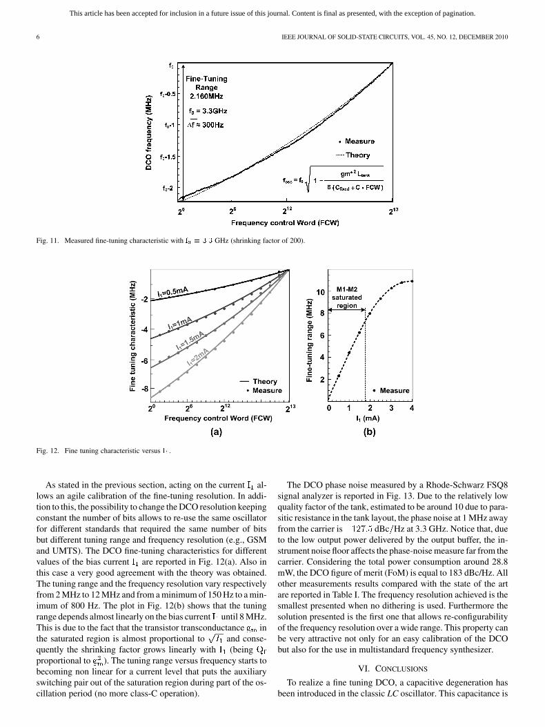
The complete scheme of the measurement setup is reportedin Fig. 10. The prototype includes a open-drain buffer that is di-rectly connected to the 50 input of a Rhode-Schwarz FSQ8signal analyzer. The delivered power to the signal analyzer wasaround . The measurement setup is automatically con-trolled by Labview® driving the prototype through a real-timecontroller NI cRio-9014. In Fig. 11 the measured fine-tuningcharacteristic is reported, showing a very good agreement withthe theory. The shrinking factor is around 200 with a fine-tuningrange of 2.160 MHz and an averaged resolution of 300 Hz (min-imum 150 Hz). In this case the current drawn by the fine-tuningbranch ( ) is around 500 A.
This article has been accepted for inclusion in a future issue of this journal. Content is final as presented, with the exception of pagination.
6 IEEE JOURNAL OF SOLID-STATE CIRCUITS, VOL. 45, NO. 12, DECEMBER 2010
Fig. 11. Measured fine-tuning characteristic with � � ��� GHz (shrinking factor of 200).
Fig. 12. Fine tuning characteristic versus � .
As stated in the previous section, acting on the current al-lows an agile calibration of the fine-tuning resolution. In addi-tion to this, the possibility to change the DCO resolution keepingconstant the number of bits allows to re-use the same oscillatorfor different standards that required the same number of bitsbut different tuning range and frequency resolution (e.g., GSMand UMTS). The DCO fine-tuning characteristics for differentvalues of the bias current are reported in Fig. 12(a). Also inthis case a very good agreement with the theory was obtained.The tuning range and the frequency resolution vary respectivelyfrom 2 MHz to 12 MHz and from a minimum of 150 Hz to a min-imum of 800 Hz. The plot in Fig. 12(b) shows that the tuningrange depends almost linearly on the bias current until 8 MHz.This is due to the fact that the transistor transconductance inthe saturated region is almost proportional to and conse-quently the shrinking factor grows linearly with (beingproportional to ). The tuning range versus frequency starts tobecoming non linear for a current level that puts the auxiliaryswitching pair out of the saturation region during part of the os-cillation period (no more class-C operation).
The DCO phase noise measured by a Rhode-Schwarz FSQ8signal analyzer is reported in Fig. 13. Due to the relatively lowquality factor of the tank, estimated to be around 10 due to para-sitic resistance in the tank layout, the phase noise at 1 MHz awayfrom the carrier is dBc Hz at 3.3 GHz. Notice that, dueto the low output power delivered by the output buffer, the in-strument noise floor affects the phase-noise measure far from thecarrier. Considering the total power consumption around 28.8mW, the DCO figure of merit (FoM) is equal to 183 dBc/Hz. Allother measurements results compared with the state of the artare reported in Table I. The frequency resolution achieved is thesmallest presented when no dithering is used. Furthermore thesolution presented is the first one that allows re-configurabilityof the frequency resolution over a wide range. This property canbe very attractive not only for an easy calibration of the DCObut also for the use in multistandard frequency synthesizer.
VI. CONCLUSIONS
To realize a fine tuning DCO, a capacitive degeneration hasbeen introduced in the classic LC oscillator. This capacitance is

This article has been accepted for inclusion in a future issue of this journal. Content is final as presented, with the exception of pagination.
FANORI et al.: CAPACITIVE DEGENERATION IN LC-TANK OSCILLATOR FOR DCO FINE-FREQUENCY TUNING 7
TABLE ISUMMARY RESULTS AND COMPARISON WITH THE STATE OF THE ART
Fig. 13. Output phase-noise measure.
reflected in parallel to the tank shrunk by a factor proportional tothe transconductance used in the cross-coupled pair. This allowsto perform a fine frequency tuning with a resolution that is notlimited by the unitary element present in the capacitor banks.
The theory presented has demonstrated the potentialities andthe limits of the structure while the measurements on prototypefor GSM application have proved its robustness.
APPENDIX I
As described by Hajimiri and Lee [12], the phase noise inthe region caused by a white noise source, at the offsetfrequency , depends on the ISF and it is given by
(9)
where is the maximum amount of dynamic charge loadedinto the tank capacitance, is the white power spectral den-sity of the noise current and is the square of the impulsesensitivity function (ISF) .
Starting from the scheme in Fig. 14, the effect of thefine tuning capacitance on the output phase noise is de-rived evaluating the ISF of the cross-coupled transistor (i.e.,
with ) and of the biascurrent generators (i.e., and with
). The phase noise associated withthe finite quality factor of the tank is not considered becauseit does not change with the capacitive degeneration of theswitching pair.
Referring to transistor M1 in Fig. 14, to find , theanalysis distinguishes three different cases related to the oper-ation mode of the differential pair, each of which is associatedwith a different ISF, i.e., both transistors work in saturation orone of them is turned off. However, the phase noise contributionof M1 differs from the classical oscillator scheme only whenboth transistors are carrying current, because in the other casesthe impulse sensitivity function is zero in both oscillator archi-tectures [13].

This article has been accepted for inclusion in a future issue of this journal. Content is final as presented, with the exception of pagination.
8 IEEE JOURNAL OF SOLID-STATE CIRCUITS, VOL. 45, NO. 12, DECEMBER 2010
Fig. 14. ISF derivation in degenerate LC oscillator.
When the two transistors work in saturation region, the noisecharge impulse present between the drain and source ofM1 produces a voltage difference between the DCO outputs thatcorresponds to the following function
(10)
where is the parasitic capacitance at the source of M1–M2.This result is very similar to the one obtained by Andreani et al.for a the classical oscillator is given by
(11)
Equation (10) differs from (11) for the presence in the denom-inator of the term which reduces the effect of theswitching transistors on the phase noise. However, as explainedin Section II, to sustain the oscillation and to achieve the desiredresolution, should be much greater than making the dif-ference between (10) and (11) negligible.
An analogous approach can be used to find the ISF of the biascurrent generators ( ). Once again itcan be proved that the new ISFs differ from the classical one( ) only when both transistor are on, being
(12)
and from [13]
(13)
Equation (12) contains once again the factor thatis not present in (13), in this case both at the numerator andat the denominator. As explained before, their contribution isirrelevant for the large used.
When only one transistor of the cross-coupled pair is on, thelarge capacitance ( ) produces a short between
and making the ISF equal to one like for the clas-sical case [13].
APPENDIX II
The contribution to the DCO phase noise due to the use of apositive conductance can be evaluated starting from theexpression of the phase noise of a traditional LC oscillator [13].In particular, this conductance is reflected in parallel to the tankobtaining
(14)
where is the phase noise of the classic LC tankoscillator and represents the tank losses. Contrary to the solu-tion proposed (that does not have any effect on the phase-noiseperformance), in this case a degradation proportional to the con-ductance occurs. Since the value of sets a constrainton the maximum fine-tuning range available ((8)) it is better torewrite (14) as follows
(15)
where is given by (8) and is the quality factor of theoriginal resonator (i.e., ). From (15) it is clear thatno penalty on the total outputs phase noise can be obtainedonly in the limit of a fine tuning range that approaches zero. Incomparison with the solution proposed, assuming for the tank
, GHz and MHz (which cor-respond to a usable tuning range of 10 MHz) the degradation ofthe phase noise is around 3 dB. This penalty is even worse if the
and/or the tuning range are increased.
ACKNOWLEDGMENT
The authors want to thank Marvell for technology access andS. Shia (TSMC) for design kit support.
REFERENCES
[1] R. B. Staszewski and P. T. Balsara, All-Digital Frequency Synthesizerin Deep-Submicron CMOS. New York: Wiley Interscience, 2006.
[2] Staszewski et al., “A digitally controlled oscillator in a 90 nm digitalCMOS process for mobile phones,” IEEE J. Solid-State Circuits, vol.40, no. 11, pp. 2203–2211, Nov. 2005.
[3] Hung et al., “A digitally controlled oscillator system for SAW-lesstransmitters in cellular handsets,” IEEE J. Solid-State Circuits, vol. 41,no. 5, pp. 1160–1170, May 2006.
[4] A. Chen et al., “9 GHz dual-mode digitally controlled oscillator forGSM/UMTS transceivers in 65 nm CMOS,” in Proc. IEEE Asian Solid-State Circuits Conf. (ASSCC’07), 2007, pp. 432–435.
[5] J. H. Han and S. H. Cho, “Digitally controlled oscillator with high fre-quency resolution using novel varactor bank,” Electronics Lett., vol. 44,no. 25, pp. 1450–1452, 2007.
[6] J. Zhuang et al., “A 3.3 GHz LC-based digitally controlled oscillatorwith 5 kHz frequency resolution,” in Proc. IEEE Asian Solid-State Cir-cuits Conf. (ASSCC’07), 2007, pp. 428–431.
[7] Pletcher and Rabaey, “A 100 �W, 1.9 GHz oscillator with fully digitalfrequency tuning,” in IEEE Int. Solid-State Circuits Conf. Dig. Tech.Papers, 2005, pp. 387–390.
[8] T. H. Lee, The Design of CMOS Radio Frequency Integrated Cir-cuits. Cambridge, U.K.: Cambridge University Press, 1998.
[9] Mazzanti and Andreani, “Class-C harmonic CMOS VCOs, with a gen-eral result on phase noise,” IEEE J. Solid-State Circuits, vol. 43, no. 12,pp. 2716–2729, Dec. 2008.

This article has been accepted for inclusion in a future issue of this journal. Content is final as presented, with the exception of pagination.
FANORI et al.: CAPACITIVE DEGENERATION IN LC-TANK OSCILLATOR FOR DCO FINE-FREQUENCY TUNING 9
[10] F. O’Mahony et al., “A 27 Gb/s forwarded-clock I/O receiver using aninjection-locked LC-DCO in 45 nm CMOS,” in IEEE Int. Solid-StateCircuits Conf. Dig., 2008, pp. 452, 627.
[11] Pittorino et al., “A UMTS-compliant fully digitally controlled oscil-lator with 100 MHz fine-tuning range in 0.13�m CMOS,” in IEEE Int.Solid-State Circuits Conf. Dig., 2006, pp. 770–779.
[12] A. Hajimiri and T. H. Lee, “A general theory of phase noise in electricaloscillators,” IEEE J. Solid-State Circuits, vol. 33, no. 2, pp. 179–194,Feb. 1998.
[13] P. Andreani et al., “A study of phase noise in colpitts and LC-tankCMOS oscillators,” IEEE J. Solid-State Circuits, vol. 40, no. 5, pp.1107–1118, May 2005.
Luca Fanori (S’10) was born in Pavia, Italy, in 1984.He received the M.Sc. degree (summa cum laude) inelectronic engineering from the University of Pavia,Italy, in 2008. Currently he is a Ph.D. candidate at theUniversity of Pavia in the Microelectronics Lab.
His research activities are focused on the imple-mentations of frequency synthesizers, in particular onDCO and all-digital PLL.
Antonio Liscidini (S’99–M’06) was born in Tirano,Italy, in 1977. He received the Laurea degree (summacum laude) and the Ph.D. in electrical engineeringfrom the University of Pavia, Pavia, Italy, in 2002 and2006, respectively.
He was a summer intern at National Semiconduc-tors, Santa Clara, CA, in 2003, studying poly-phasefilters and CMOS LNA. Currently, he is an AssistantProfessor at the University of Pavia. His researchinterests are in the implementations of analog RFfront-end in CMOS and BiCMOS technology, with
particular focus on the analysis and design of LNAs for multi-standard applica-tions, ultra-low-power receivers and digital PLLs. In addition to his academicactivities, he has been acting as a consultant for Marvell Semiconductors in thearea of integrated circuit design.
Dr. Liscidini received the Best Student Paper Award at IEEE 2005 Sympo-sium on VLSI Circuits. Since December 2007, he has served as an AssociateEditor of the IEEE TRANSACTIONS ON CIRCUITS AND SYSTEMS II: EXPRESS
BRIEFS, and since 2010 he has been a member of the TPC of the European SolidState Circuits Conference (ESSCIRC).
Rinaldo Castello (S’78–M’78–SM’92–F’99) grad-uated from the University of Genova (summa cumlaude) in 1977 and received the M.S. and Ph.D. de-grees from the University of California, Berkeley, in1981 and 1984, respectively.
From 1983 to 1985 he was Visiting AssistantProfessor at the University of California, Berkeley.In 1987 he joined the University of Pavia, Italy,where he is now a Full Professor. He consulted forST-Microelectronics, Milan, Italy, up to 2005 andfrom 1998 to 2005 was the Scientific Director of a
joint research center between the University of Pavia and ST. He promoted theestablishing of several design centre from multinational IC companies in thePavia area, among them Marvell, for which he has been consulting from 2005.
Dr. Castello has been a member of the TPC of the European Solid StateCircuits Conference (ESSCIRC) since 1987 and of the IEEE InternationalSolid State Circuits Conference (ISSCC) from 1992 to 2004. He was TechnicalChairman of ESSCIRC’91 and General Chairman of ESSCIRC’02, AssociateEditor for Europe of the IEEE JOURNAL OF SOLID-STATE CIRCUITS from 1994to 1996 and Guest Editor of the July 1992 special issue. From 2000 to 2007he has been Distinguished Lecturer of the IEEE Solid State Circuit Society.He was named one of the outstanding contributors for the first 50 years ofthe ISSCC and a co-recipient of the Best Student Paper Award at the 2005Symposium on VLSI.