ie1204 answers exam af 2021-05-17 copy 0
TRANSCRIPT

IE1204 Digital Design Answer Form 2021-05-17
Program
NN
# Answer with Points
1 Decimal number1
2 8 bit two's complement binary number 0 1 1 1 1 0 1 1 1
3 8 bit two's complement binary number 1 1 0 0 0 0 0 1 1
4 Boolean expression, Y =1
51
61
MUX connections
CD = 00
CD = 01
CD = 10
CD = 11
8
1
9
1
Yes No
Yes No
11 Boolean expression (Hazard fix only)1
16 bit two's complement binary number, MSB 1 1 1 1 1 1 1 0
LSB 0 1 1 1 1 0 0 0
13 8 bit two's complement binary number 1 1 1 0 1 1 1 1 1
14 Number interval1
15 1 0 0 0 0 1
16 0 0 0 1 1
16
1
‐8 to 7.9375
5 result bits (S4 S3 S2 S1 S0)
4 flag bits (V C N Z)
(A+BD)C
1
Boolean expression, Y =
Boolean expression, Y =
OR
TOTAL POINTS Examiner sign
CMZ
Timing diagram
Timing diagram
10 Setup condition
Hold condition
12
C D
7 0
1A B
A + B
A
‐113
Full Name Personal Number
Exam Answers 2021‐05‐17 00000000 = 0
Answer
𝑌 𝐴 𝐵 𝐶 𝐴 𝐵 𝐶 𝐴 𝐵 𝐶 𝐵 𝐶 𝐴 𝐵
𝑌 𝐴 · 𝐶 𝐶 · 𝐷 𝐵 · 𝐶𝑌 𝐶 𝐷 𝐴 𝐵 𝐶
0 ms 5 ms 10 ms 15 ms 20 ms 25 ms 30 ms 35 ms 40 ms 45 ms
CLK
Q
0 ms 5 ms 10 ms 15 ms 20 ms 25 ms 30 ms 35 ms 40 ms 45 ms
CLK
Q

2021-05-17 0 IE1204
IE1204 Digital Design Exam 2021-05-17 K-maps
4 CMOS
Swedish: Bestäm den logiska funktionen Y = f(A, B, C, D) för CMOS-grindnätet. Förenkla så långt som möjligt. English: Determine the logic function Y = f(A, B, C, D) for the CMOS-circuit. Simplify as much as possible.

2021-05-17 0 IE1204
5 SoP / PoS
Swedish: Ta fram booleskt uttryck på PoS form för sanningstabellen nedan. English: Derive the Boolean expression in PoS form for the truth table below.
A B C Y
0 0 0 1
0 0 1 1
0 1 0 0
0 1 1 1
1 0 0 1
1 0 1 1
1 1 0 0
1 1 1 0
2021-05-17 0 IE1204
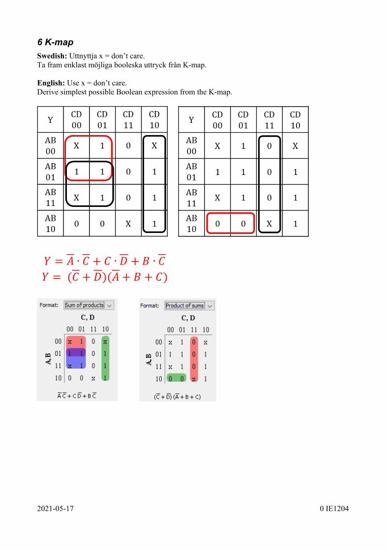
6 K-map
Swedish: Uttnyttja x = don’t care. Ta fram enklast möjliga booleska uttryck från K-map. English: Use x = don’t care. Derive simplest possible Boolean expression from the K-map.
𝑌 𝐴 ∙ 𝐶 𝐶 ∙ 𝐷 𝐵 ∙ 𝐶
𝑌 𝐶 𝐷 𝐴 𝐵 𝐶
1
IE1204 Digital Design Exam 2021-05-17 Solutions
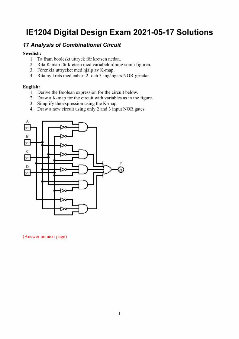
17 Analysis of Combinational Circuit
Swedish: 1. Ta fram booleskt uttryck för kretsen nedan. 2. Rita K-map för kretsen med variabelordning som i figuren. 3. Förenkla uttrycket med hjälp av K-map. 4. Rita ny krets med enbart 2- och 3-ingångars NOR-grindar.
English:
1. Derive the Boolean expression for the circuit below. 2. Draw a K-map for the circuit with variables as in the figure. 3. Simplify the expression using the K-map. 4. Draw a new circuit using only 2 and 3 input NOR gates.
(Answer on next page)

2
Use POS for NOR only (inverters are ok if you note that they can be made with a NOR) No deductions if not simplest possible.
For POS, draw 𝑌 𝐵 𝐷 𝐵 𝐷 𝐵 𝐷 𝐵 𝐷
For SOP, draw 𝑌 𝐵 ∙ 𝐷 𝐵 ∙ 𝐷 𝐵 𝐷 𝐵 𝐷 (Note the double inversion bars, an extra inverter/NOR is needed)
CD =
00 01 11 10
AB = 00 0 1 1 0
01 1 0 0 1
11 1 0 0 1
10 0 1 1 0

3
18 Design of Combinational Circuit
Swedish: Designa en kombinatorisk krets för Y=f(Q3, Q2, Q1, Q0), Q3 = MSB där
Y = 1 för 3, 4, 10, 13 Y = x (don’t care) för 1, 2, 5, 9, 11, 12 Y = 0 för alla övriga tal
1. Rita sanningstabellen. 2. Rita K-map för sanningstabellen med variabelordning som i figuren. 3. Uttnyttja x = don’t care. Ta fram enklast möjliga booleska uttryck från K-map. 4. Rita en krets för uttrycket med enbart NAND-grindar.
English: Design a combinational circuit for Y=f(Q3, Q2, Q1, Q0), Q3 = MSB where
Y = 1 for 3, 4, 10, and 13 Y = x (don’t care) for 1, 2, 5, 9, 11, and 12 Y = 0 for all other numbers
1. Draw the truth table. 2. Draw a K-map for the truth table with variables as in the figure.. 3. Use x = don’t care. Derive simplest possible Boolean expression from the K-map. 4. Draw a circuit for the expression using only NAND-gates.
(Answer on next page)
Q1Q0 =
00 01 11 10
Q3Q2 =
00
01
11
10
Rita om K-map i dina inlämnade svar. Redraw the K-map in your answer sheets.

4
18 Design of Combinational Circuit
Use SOP for NAND only (inverters are ok if you note that they can be made with a NAND) No deductions if not simplest possible.
For SOP draw 𝑌 𝑄2 ∙ 𝑄1 𝑄2 ∙ 𝑄1 𝑄2 ∙ 𝑄1 ∙ 𝑄2 ∙ 𝑄1
For POS draw 𝑌 𝑄2 𝑄1 ∙ 𝑄2 𝑄1 𝑄2 ∙ 𝑄1 ∙ 𝑄2 ∙ 𝑄1
(Note the double inversion bars, an extra inverter/NAND is needed)

5
19 Analysis of FSM
Swedish: Analysera vad nedanstående tillståndsmaskin (FSM) utför. 1. Ta fram Boolska uttryck för nästa tillstånd. 2. Rita tillståndstabell. 3. Rita tillståndsdiagram.
Använd ordningen Q2:0 English: Analyze the state machine (FSM) below.
1. Derive Boolean expressions for next state. 2. Draw a state table. 3. Draw a state diagram.
Use the order Q2:0
𝑄2 𝐴 ∙ 𝑄1 ∙ 𝑄0 𝐴 ∙ 𝑄2 𝑄2 ∙ 𝑄0 𝑄2 ∙ 𝑄1 𝑄1 𝐴 ∙ 𝑄1 ∙ 𝑄0 𝐴 ∙ 𝑄1 ∙ 𝑄0 𝐴 ∙ 𝑄2 ∙ 𝑄1 𝐴 ∙ 𝑄1 ∙ 𝑄0 𝐴 ∙ 𝑄2 ∙ 𝑄1 ∙ 𝑄0 𝑄0 𝐴 ∙ 𝑄0 𝑄1 ∙ 𝑄0 𝑄2 ∙ 𝑄0 𝐴 ∙ 𝑄2 ∙ 𝑄1

6
If A=0: count up and stop at 7 If A=1: count down and stop at 0
Present state Next state A = 0 Next state A = 1
Q2 Q1 Q0 Q2+ Q1+ Q0+ Q2+ Q1+ Q0+
0 0 0 0 0 1 0 0 0
0 0 1 0 1 0 0 0 0
0 1 0 0 1 1 0 0 1
0 1 1 1 0 0 0 1 0
1 0 0 1 0 1 0 1 1
1 0 1 1 1 0 1 0 0
1 1 0 1 1 1 1 0 1
1 1 1 1 1 1 1 1 0

7
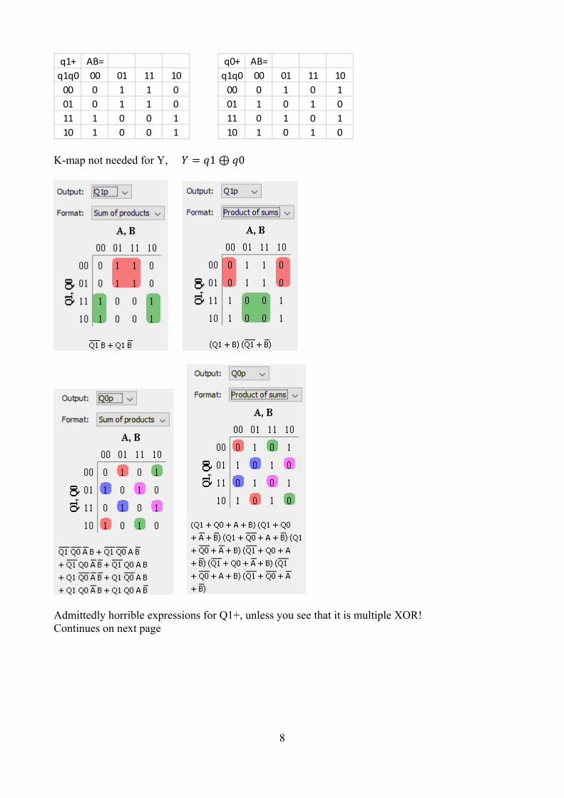
20 Design of FSM
Swedish: Konstruera en tillståndsmaskin (FSM) enligt tillståndsdiagrammet nedan. 1. Rita tillståndstabell. 2. Ta fram K-map för nästa tillstånd. 3. Ta fram minimerade uttryck för nästa tillstånd och utsignal. 4. Rita kretsschema för en FSM med DFFs och vilka grindar som helst.
English: Design a state machine (FSM) according to the state diagram below.
1. Draw a state table. 2. Derive K-maps for next states. 3. Derive minimized expressions for next state and output. 4. Draw the FSM circuit diagram with DFFs and any gates.
Next state
Present state AB = 00 AB = 01 AB = 11 AB = 10 Out
q1 q0 q1+ q0+ q1+ q0+ q1+ q0+ q1+ q0+ Y
0 0 0 0 1 1 1 0 0 1 0
0 1 0 1 1 0 1 1 0 0 1
1 1 1 0 0 1 0 0 1 1 0
1 0 1 1 0 0 0 1 1 0 1
Rita om K-map i dina inlämnade svar. Redraw the K-map in your answer sheets.
A B =
00 01 11 10
q1q0
= 00
01
11
10
8
K-map not needed for Y, 𝑌 𝑞1 ⊕𝑞0
Admittedly horrible expressions for Q1+, unless you see that it is multiple XOR! Continues on next page
q1+ AB=
q1q0 00 01 11 10
00 0 1 1 0
01 0 1 1 0
11 1 0 0 1
10 1 0 0 1
q0+ AB=
q1q0 00 01 11 10
00 0 1 0 1
01 1 0 1 0
11 0 1 0 1
10 1 0 1 0

9
Otherwise it is very complicated: