id 215c: usb 3.0 super speed – “under the hood” management software, compliance testing, usb...
TRANSCRIPT

1
Renesas Electronics America Inc.
© 2010 Renesas Electronics America Inc. All rights reserved.
ID 215C: USB 3.0 Super Speed –“Under the Hood”
Dave W. Johnson
Staff Applications Engineer
12 October 2010
Version: 1.7
• USB 3.0 is the next generation in USB technology, offering up to 10X speed improvement over the ubiquitous USB 2.0 technology. This session will describe the electrical and packet protocol levels in some detail, including an overview of test methods for assuring electrical signal integrity and capturing and analyzing data packet traffic. Attendees will receive a thorough overview of what USB 3.0 is all about as well as the more detailed technical explanations.

2
2 © 2010 Renesas Electronics America Inc. All rights reserved.
Mr. Dave W. Johnson
Staff Applications Engineer
Tech Support for USB 3.0 and 2.0
Tech Support for PCI Express
6 years at Renesas and NEC
Photo
Goes
Here
Previous Industry Experience, 33 years
Board design, digital & analog
Data communications
MPU-based designs
Software
Tech Support for personal computer chipsets
• At Renesas (formerly NEC Electronics), I have been responsible for providing technical support for chip-level USB and PCIe products.
• This has included the whole range of USB 2.0 devices such as the µPD720101 and µPD720102 host controllers, µPD720114 hub, µPD720133 IDE bridge and µPD720150 host/peripheral controller. I also supported the µPD720400 and µPD720404 PCI Express to PCI-X bridges, µPD720401 and µPD720403 PCI Express switches, and two Wireless USB 2.0 devices (host and hub).
• My experience prior to NEC (now Renesas) included technical support for digital camera VLSI devices and data communications (pre-Ethernet) as well as PC core logic and graphics devices. I am still learning about the more modern microcontrollers available today from Renesas, since all of my more recent experience has focused on peripheral devices for Intel-Microsoft compatible personal computers.

3
3 © 2010 Renesas Electronics America Inc. All rights reserved.
Renesas Technology and Solution Portfolio
Microcontrollers
& Microprocessors#1 Market share
worldwide *
Analog and
Power Devices#1 Market share
in low-voltage
MOSFET**
Solutions
for
Innovation
Solutions
for
InnovationASIC, ASSP
& MemoryAdvanced and
proven technologies
* MCU: 31% revenue
basis from Gartner
"Semiconductor
Applications Worldwide
Annual Market Share:
Database" 25
March 2010
** Power MOSFET: 17.1%
on unit basis from
Marketing Eye 2009
(17.1% on unit basis).
In the session 110C, Renesas Next Generation Microcontroller and Microprocessor Technology Roadmap, Ritesh Tyagi introduces this high level image of where the Renesas Products fit. The big picture.

4
4 © 2010 Renesas Electronics America Inc. All rights reserved.
4
Microcontrollers
& Microprocessors#1 Market share
worldwide *
Analog and
Power Devices#1 Market share
in low-voltage
MOSFET**
Solutions
for
Innovation
Solutions
for
InnovationASIC, ASSP
& MemoryAdvanced
and proven
technologies * MCU: 31% revenue
basis from Gartner
"Semiconductor
Applications Worldwide
Annual Market Share:
Database" 25
March 2010
** Power MOSFET: 17.1%
on unit basis from
Marketing Eye 2009
(17.1% on unit basis).
Renesas Technology and Solution Portfolio
This is where our session, 215C, USB 3.0 Super Speed, is focused within the ‘Big picture of Renesas Products’
Specifically, USB 3.0 technology falls into the “Connectivity Products” category of ASSP and ASIC devices from Renesas.
“ASSP” refers to Application Specific Standard Products, and “ASIC” refers to Application Specific Integrated Circuits (custom products developed jointly with technology partners).

5
5 © 2010 Renesas Electronics America Inc. All rights reserved.
Innovation: 10X Faster File Transfer
70 sec
HD Movie25 Gbyte
14 minutes for USB 2.0 HS
USB 3.0 is a great enabler for faster file transfers to and from PC mass storage media and today’s modern handheld storage and display/communication devices. The slide shows the dramatic difference in speed between USB 2.0 and USB 3.0 for loading a 25 GB high-definition movie onto a portable storage and playback device. The less time a user has to spend waiting for such transfers, the happier the user will be. And the higher-definition movies that now become practical to transfer make users happier, as well, enriching their overall living experience.

6
6 © 2010 Renesas Electronics America Inc. All rights reserved.
Our USB 3.0 Solution
Add USB 3.0 ports to existing PCs
Do more work in less time
Make user happy!
• The uPD720200 device from Renesas Electronics enables USB 3.0 host ports on existing PCs. The user can insert an ExpressCard into a laptop card slot and thereby add two USB 3.0 ports to his laptop.
• Similarly, a desktop PC user can insert a PCI Express add-in card into his PC and thereby add two USB 3.0 ports to his desktop PC.
• The Super Speed of USB 3.0 then allows the user to do more work in less time, and anything that saves time can be of great value to users.
7
7 © 2010 Renesas Electronics America Inc. All rights reserved.
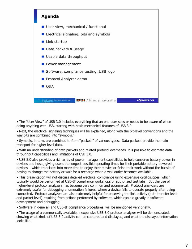
Agenda
User view, mechanical / functional
Electrical signaling, bits and symbols
Link startup
Data packets & usage
Usable data throughput
Power management
Software, compliance testing, USB logo
Protocol Analyzer demo
Q&A
• The “User View” of USB 3.0 includes everything that an end user sees or needs to be aware of when doing anything with USB, starting with basic mechanical features of USB 3.0.
• Next, the electrical signaling techniques will be explained, along with the bit-level conventions and the way bits are combined into “symbols.”
• Symbols, in turn, are combined to form “packets” of various types. Data packets provide the main transport for higher level data.
• With an understanding of data packets and related protocol overheads, it is possible to estimate data throughput capabilities and limitations of USB 3.0.
• USB 3.0 also provides a rich array of power management capabilities to help conserve battery power in devices and hosts, giving users the longest possible operating times for their portable battery-powered devices – which translates into more time to enjoy their movies or finish their work without the hassle of having to change the battery or wait for a recharge when a wall outlet becomes available.
• This presentation will not discuss detailed electrical compliance using expensive oscilloscopes, which typically would be performed at USB-IF compliance workshops or authorized test labs. But the use ofhigher-level protocol analyzers has become very common and economical. Protocol analyzers are extremely useful for debugging enumeration failures, where a device fails to operate properly after being connected. Protocol analyzers are also extremely helpful for observing the link activity (both transfer level and packet level) resulting from actions performed by software, which can aid greatly in software development and debugging.
• Software in general, and USB-IF compliance procedures, will be mentioned very briefly.
• The usage of a commercially available, inexpensive USB 3.0 protocol analyzer will be demonstrated, showing what kinds of USB 3.0 activity can be captured and displayed, and what the displayed information looks like.

8
8 © 2010 Renesas Electronics America Inc. All rights reserved.
Key Takeaways
Strengths of the USB 3.0 interface
Where the USB 3.0 interface should be used
Software and hardware tools
Devices from Renesas
We hope that this session will provide a basic technical foundation for evaluating USB 3.0 for microcontroller-based applications as well as for PC systems.

99
9 © 2010 Renesas Electronics America Inc. All rights reserved.
9
USB 3.0 from Renesas
PCI
ExpressUSB 2.0
PHY
Roo
thu
b
xHCI
PCI
Express
USB 3.0
PHY
Port1
Port2
Port1
Port2
µPD720200
World’s first
USB 3.0
Connectors
Port1
Port2
PCI
ExpressUSB 2.0
PHY
Roo
thu
b
xHCI
PCI
Express
USB 3.0
PHY
Port1
Port2
Port1
Port2
µPD720200
World’s first
USB 3.0
Connectors
Port1
Port2
• The USB 3.0 device currently available from Renesas is the µPD720200 (and its successor, the µPD720200A). This device is a USB 3.0 Host Controller. A system designer can design it onto a PC motherboard or add-in card to provide a bridge from a PCI Express interface to two USB 3.0 host ports.
• Product Name: µPD720200F1-DAK-A
• System I/F: PCI Express 2.0 x 1 Lane
• USB ports: 2 ports (SS/HS/FS/LS)
• Complies with: PCI Express 2.0 Base Spec, USB 3.0 rev1.0, Intel xHCI rev0.96
• Supply voltages: 1.05V and 3.3V
• This device interfaces to the host CPU (or, potentially, MCU) using a PCI Express “Gen 2”single-lane interface running at either 2.5 Gbps or 5.0 Gbps.
• As we will see shortly on subsequent slides, a USB 3.0 interface requires two sets of signals: a USB 2.0 compatible group, for USB 2.0 compatibility, and a new “Super Speed” group of signals enabling the greatly increased speed of USB 3.0.
• To utilize this particular device effectively in a system design, the system will need (a) a one-lane PCI Express bus, (b) system memory or other data source/sink that is fast enough to sustain up to 500 MB/sec transfer rate (or at least 30 or 40 MB/sec minimum, beyond USB 2.0 HS), and (c ) an attached device that supports USB 3.0. These requirements are readily satisfied in PC systems but tend to be less common in MCU-based designs so far.
• This device (µPD720200) was the world’s first single-chip USB 3.0 Host Controller. It implements the xHCI software standard (rev. 0.96).
10
10 © 2010 Renesas Electronics America Inc. All rights reserved.
10
Shipping 2 million per month since April 2010
Renesas Electronics (TSE: 6723) today announced that it
plans to double production of its USB Implementers Forum
(USB-IF) certified SuperSpeed USB (USB 3.0) host
controller (part number µPD720200), the world’s first, and
is expecting to reach monthly production of two million
units starting April 2010.
KAWASAKI (Japan), SANTA CLARA, Calif. (USA),
DUESSELDORF (Germany), March 17, 2010
• Because the µPD720200 was the first USB 3.0 Host Controller to reach the market, it has enjoyed great success. As of April of this year, it was already shipping at the rate of 2 million units per month, mainly for personal computers and similar devices running Windows or comparable operating systems.
• As of August 2010, the µPD720200 and µPD720200A were still the only USB 3.0 Host Controller devices to have received USB-IF certification for the USB 3.0 logo.
10

11
11 © 2010 Renesas Electronics America Inc. All rights reserved.
SuperSpeed for Hard Disk Drives
RenesasRenesas
RenesasRenesas
LucidPort USB300: USB 3.0 to SATA II Bridge
Press release from NEC Electronics, now merged into Renesas Electronics:
KAWASAKI (Japan), SANTA CLARA, Calif. (USA), DUESSELDORF (Germany), September 24, 2009
NEC Electronics today announced the availability of a Universal Serial Bus (USB) 3.0 system-on-a-chip (SOC) design solution that customers can use to kick start the development of custom USB 3.0 products. Leveraging NEC Electronics' design, implementation and manufacturing strengths as a leading integrated device manufacturer (IDM), the SOC design solution helps to reduce risk, improve efficiency and speed time to market, while allowing customers to focus on developing their own differentiated logic.
The SOC design solution features NEC Electronics' USB 3.0 intellectual property (IP) core, which is fully interoperable with the company's recently USB-IF-certified USB 3.0 host controller (part number µPD720200) and also backward compatible with previous versions of the USB standard. NEC Electronics expects rapid adoption of the solution by customers developing mass storage, display and video applications, especially as the need to transfer larger and larger amounts of information from PCs to external hard-drives, portable electronics devices, and flash-based drives continues to grow.
LucidPort Technology, a fabless semiconductor company developing SuperSpeed USB and Wireless USB controllers, leveraged NEC Electronics USB 3.0 SOC design solution in the development of itsUSB300, a single chip USB 3.0 to SATA-II bridge designed for external storage devices.
"Working with NEC Electronics' USB 3.0 SOC design solution with the industry's first USB 3.0 core, we were able to bring our bridge chip to market quickly," said Reid Augustin, vice president, product development for LucidPort. "NEC Electronics provided engineering support for each stage of design and manufacturing, and ensured the interoperability of the basic building blocks, freeing up our designers to focus on developing our specific application logic."
"NEC Electronics has earned a reputation for delivering dedicated customer service and high-quality, reliable custom products. In fact, these qualities are cornerstones of the NEC Electronics culture," said Osamu Matsushima, general manager, ASIC Solutions Division, NEC Electronics Corporation. "Combining our USB leadership with our years of experience delivering custom SOC and standard solutions, the new SOC design solution provides customers with a one-stop-shop for implementing their system solutions on time and within budget.“

1212
12 © 2010 Renesas Electronics America Inc. All rights reserved.
12
0
50,000
100,000
150,000
200,000
250,000
300,000
350,000
400,000
2009 2010 2011 2012 2013
Desktop & Mobile PC TAM Total w/ SuperSpeed USB
Unit Shipments in Thousands
Source: In-Stat, 7/09
Made successful market penetration for high-end PCs in CY2009
Focus in CY10 is on mid-range PC designs for production in CY2011
PC TAM and USB 3.0 Penetration
Expansion to
Business PC
Chipset
Integration
Expansion to
Consumer PC
260M
15M
280M
100M
325M
240M
370M365M
USB 3.0 market forecast for PCs
The total market for USB 3.0 is expected to grow steadily in the coming years, with the greatest volumes occurring when personal computer manufacturers begin including USB 3.0 support in their core logic chipsets.

13
13 © 2010 Renesas Electronics America Inc. All rights reserved.
Host
(Root Hub)
External
Hub
Device
0 to 5 levels
Contains
“Functions” and
“Endpoints”USB Cable
USB
Cable
Upstream port?
Downstream port?
Includes USB
“Host Controller”
Device
USB
CableOptional
Upstream port?
Downstream port?
Basic USB Topology
• A Host Controller, also known as a Root Hub, provides a bridge from a host system bus (such as PCI Express) to one or more USB ports.
• Each Host port connects by USB cable to one USB Device or External Hub.
• In USB, the Host (Root Hub) is the central “master” for all data flow in the topology. The Host initiates all data flow to or from the Host. Devices or external hubs attached to the Host are “slaves” for data flow control. The ports on the Host are always “master” ports, and the port on an endpoint device is always a “slave” port.
• Each external hub that may be present has one “slave” port facing toward the Host, and one or more “master” ports facing away from the host.
• The USB 3.0 Specification, Chapter 2, defines the direction of data flow control as “upstream” (toward the host) or “downstream” (away from the host). To be precise, “upstream” and “downstream” here refer to “upstream direction” and “downstream direction.” “Direction,” in turn, refers to data flow control, master vs. slave.
• An “upstream-facing port” is a slave port that faces toward the Host, and a “downstream-facing port” is a master port that faces away from the Host.
• The USB 3.0 Specification also defines an “upstream port” as the same as an upstream-facing port (toward the Host), and a “downstream port” is the same as a downstream-facing port.
• Note that a host port is a “downstream” port, not an “upstream port,” because it faces downstream. Similarly, a device port is an “upstream” port because it faces upstream.
14
14 © 2010 Renesas Electronics America Inc. All rights reserved.
14
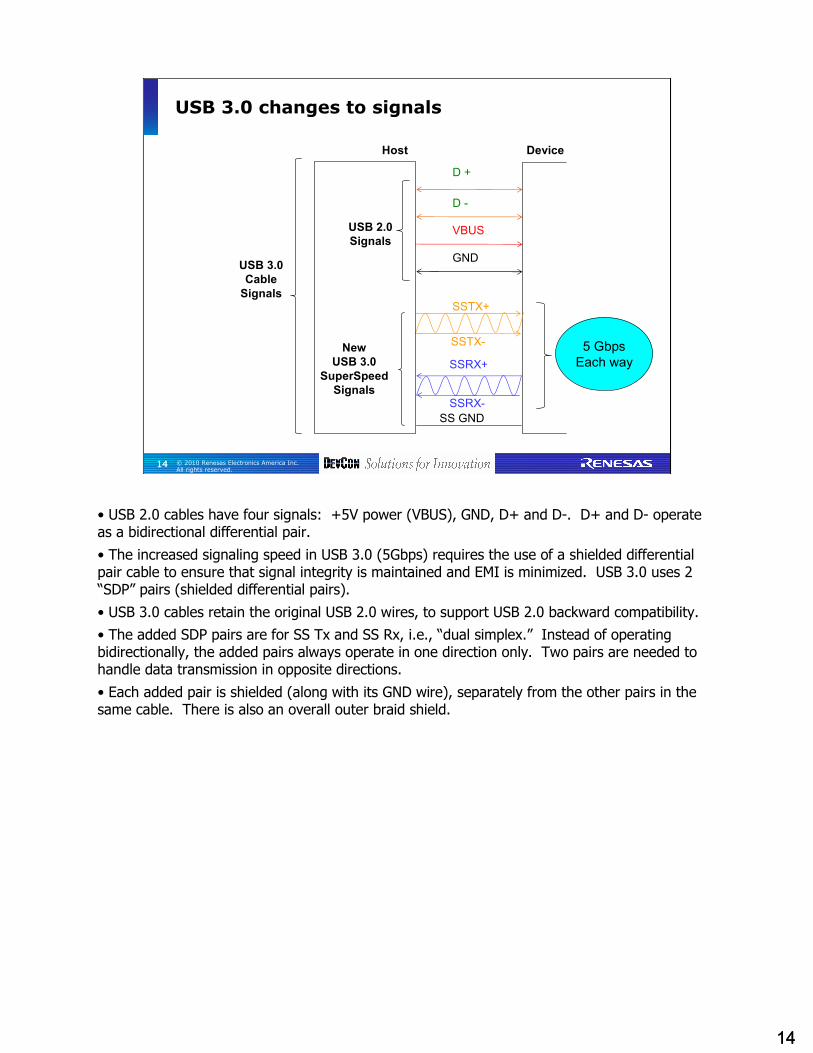
USB 3.0 changes to signals
Host Device
D +
D -
VBUS
GND
USB 2.0
Signals
New
USB 3.0
SuperSpeed
Signals
USB 3.0
Cable
SignalsSSTX+
SSTX-
SSRX+
SSRX-
SS GND
5 Gbps
Each way
• USB 2.0 cables have four signals: +5V power (VBUS), GND, D+ and D-. D+ and D- operate as a bidirectional differential pair.
• The increased signaling speed in USB 3.0 (5Gbps) requires the use of a shielded differential pair cable to ensure that signal integrity is maintained and EMI is minimized. USB 3.0 uses 2 “SDP” pairs (shielded differential pairs).
• USB 3.0 cables retain the original USB 2.0 wires, to support USB 2.0 backward compatibility.
• The added SDP pairs are for SS Tx and SS Rx, i.e., “dual simplex.” Instead of operating bidirectionally, the added pairs always operate in one direction only. Two pairs are needed to handle data transmission in opposite directions.
• Each added pair is shielded (along with its GND wire), separately from the other pairs in the same cable. There is also an overall outer braid shield.
14

15
15 © 2010 Renesas Electronics America Inc. All rights reserved.
USB 3.0 Cable ConstructionFor HS (480 Mbps), FS
(12 Mbps), LS (1.5 Mbps)
For SS (5.0 Gbps)
For SS (5.0 Gbps)
For HS (480 Mbps), FS
(12 Mbps), LS (1.5 Mbps)
For SS (5.0 Gbps)
For SS (5.0 Gbps)
Source: USB 3.0
Specification, Figure 5-15
• This diagram is from the USB 3.0 Specification (Rev. 1.0), Figure 5-15. The accompanying text explains, “There are three groups of wires: UTP signal pair, Shielded Differential Pair (SDP, twisted or twinax differential pairs), and power and ground wires.”
• This is a cross-section view of USB 3.0 cable construction. “UTP” means “unshielded twisted pair.” The UTP pair handles the three USB 2.0 data speeds, known as HS, FS and LS.
• HS (high speed, 480 Mbps) is faster than FS (full speed, 12 Mbps), in USB terminology.

161616
16 © 2010 Renesas Electronics America Inc. All rights reserved.
16
USB 2.0 cables and connectors
Male
Micro
Type-B
Male
Mini
Type-B
Male
Regular
Type-B
Female
Type-AMale
Type-A
• These are typical connectors used on USB 2.0 cables. Some additional types are added for USB 3.0 (see next slide).
• This slide also shows the “A” and “B” connector differences, corresponding to downstream-facing and upstream-facing ports, respectively.
• In other words, “A” refers to the host (or upstream Hub) end of a cable. “B” refers to the Device (or downstream hub) end.
• As noted on an earlier slide, the “upstream end” of a cable (A-connector) connects to a “downstream-facing” USB port on a host or hub, and the “downstream end” of a cable (B-connector) connects to an “upstream-facing” USB port on a hub or device.

17
17 © 2010 Renesas Electronics America Inc. All rights reserved.
Standard-A USB 3.0 Receptacle and Plug
Blue Color
Standard-A
Receptacle Standard-A
Plug
USB 3.0
Cable
Blue Color
Standard-A
Receptacle Standard-A
Plug
USB 3.0
Cable
• “Plug” in USB terminology refers to a “male” connector, and “receptacle” refers to a female connector.
• This slide shows the Standard-A receptacle and plug for USB 3.0. They look outwardly very similar to the USB 2.0 Standard-A plug and receptacle, except for the distinctive blue color of the main insulator that prevents upside-down insertion of the plug. Blue is intended to be used for USB 3.0, while white or black are typically used for USB 2.0.
• Although it’s not visible in this view, there are actually five additional pins in these connectors, compared to USB 2.0. The next slide shows this more clearly.
• The similarity of these connectors to USB 2.0 counterparts is intentional, to allow USB 3.0 plugs to be inserted into USB 2.0 receptacles, and vice versa.
• The compatibility of USB 2.0 and USB 3.0 connectors applies to Standard-A connectors. The situation with Standard-B connectors is a little different, as shown on a later slide.
• Unless otherwise noted, all diagrams and tables with a figure number or table number in this presentation are taken from the USB 3.0 Specification. The Specification numbering has been preserved to facilitate locating the information in the USB 3.0 Specification in case there is ever a need to review additional details of the material.

18
18 © 2010 Renesas Electronics America Inc. All rights reserved.
USB3.0 Connector Compatibility
Existing USB2.0 signaling
New USB3.0 SuperSpeed signaling
USB3.0 A connecter has same form factor as in USB2.0
• The Standard-A USB 3.0 plug has five additional pins, compared to USB 2.0.
• Four pins are needed for the two added differential pairs (SSTX, SSRX).
• The 5th pin connects to the two added SS GND wires in the cable.
• In the plug, the 5 added SS pins are recessed inside the back of the plug and do not make contact with anything if the USB 3.0 plug is inserted into a USB 2.0 Standard-A receptacle.
• The mechanical design of the USB 3.0 Standard-A receptacle also assures that the USB 3.0 pins never make contact with the USB 2.0 pins, not even momentarily as the plug is inserted into or removed from the receptacle.
• Note again the color of USB 3.0 – blue.

191919
19 © 2010 Renesas Electronics America Inc. All rights reserved.
19
USB 3.0 changes to PCB and cables and connectors (examples)
USB 3.0 StandardUSB 3.0 Standard--B (Blue Color)B (Blue Color)
USB 2.0 portion
USB 3.0 portion
USB 3.0 MicroUSB 3.0 Micro--BB
USB 2.0 portion
USB 3.0 portion
• The left example shows the USB 3.0 Standard-B plug and receptacle. The USB 3.0 SS signals have been added in the top section of the plug and receptacle. This added top section makes the USB 3.0 Standard-B plug mechanically incompatible with the USB 2.0 Standard-B receptacle, but normally a USB 2.0 Standard-B cable would be used with a USB 2.0 device in any case.
• The example on the right shows the USB 3.0 Micro-B receptacle and plug. The USB 3.0 SS signals have been added on the left side of the receptacle. The right side of the USB 3.0 Micro-B receptacle can accept the USB 2.0 Micro-B plug.
• The USB 3.0 Micro-B plug is mechanically incompatible with the USB 2.0 Micro-B receptacle because of the added SS section for USB 3.0.

20
20 © 2010 Renesas Electronics America Inc. All rights reserved.
USB 3.0 Supports USB 2.0
USB 2.0 Standard-A
USB 3.0 Standard-A
USB 2.0 Standard-B
USB 3.0 Standard-B
USB 3.0 Powered-B
USB 2.0 Micro-B
USB 3.0 Micro-B
USB 2.0 Micro-AB
USB 3.0 Micro-AB
USB 2.0 Micro-A
USB 3.0 Micro-A
Receptacles Plugs
Reference: USB 3.0 Specification, Table 5-1
USB3 vs. USB2
A vs. B
Powered-B
Host-to-Host
OTG ID
Cable length
• This is a diagrammatic representation of the information contained in Table 5-1 in the USB 3.0 Specification, showing all the receptacles and plugs that are defined in USB 3.0 and which plugs can be used in which receptacles.
• Blue color refers to USB 3.0, while gray color refers to USB 2.0. The squares on the left represent receptacles, and the diamonds on the right represent plugs.
• The main difference between USB 2.0 connectors and USB 3.0 connectors is the presence of the SS signals for USB 3.0.
• The main difference between an “A” receptacle and a “B” receptacle is whether VBUS (+5V power) is supplied or received.
• Except in the “powered B” case, a “B” receptacle must never supply +5V power. Devices in USB normally receive power; they do not source it.
• The Powered-B case allows a self-powered device such as a printer to provide power to a wireless USB hub dongle. It contains a separate, additional VBUS pin for that purpose.
• With only one exception in USB 3.0, an “A” receptacle (host port) must never be connected directly to another “A” receptacle (host port). The exception is the Host-to-Host cable defined in USB 3.0 for connecting the SS signals between two hosts. The USB 2.0 signals in that cable are not connected.
• The Micro family of connectors also include a signal for OTG ID. “OTG” refers to “On the Go,”a mode of USB in which the same receptacle can act either as a host port or a device port, depending on what is connected to the port.
• USB 3.0 does not specify a maximum cable length. Instead, maximum loss budgets are defined for SS signaling and power. Most well designed USB 3.0 cables will probably have a resulting length limit of about 3 meters.
21
21 © 2010 Renesas Electronics America Inc. All rights reserved.
Question
Question 1: What color is USB 3.0?
Answer 1: Blue.
Actually, the connector alignment insert is blue.
The rest of the connectors and cable can be whatever color the manufacturer chooses – typically black, gray, white, blue, etc., just like USB 2.0.
22
22 © 2010 Renesas Electronics America Inc. All rights reserved.
Big Picture: Types of Link Activity
Electrical Idle
Low Frequency
Periodic
Signaling
(LFPS)
Training
Sequences
(5 Gbps)
Logical idle
(5 Gbps)
• Data Packet Header & Payload (DPH, DPP)
• Transaction Packets (TP)
• Isochronous Timestamp Packets (ITP)
• Link Management Packets (LMP)
• Link Command Packets
Packets (5 Gbps)
Reset
Pow
er S
avin
g
Diagnostic
Sequences
(5 Gbps)
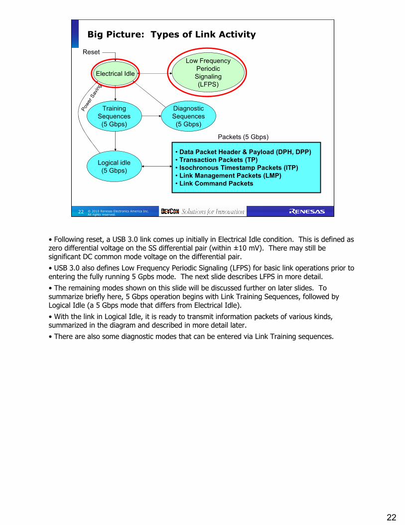
• Following reset, a USB 3.0 link comes up initially in Electrical Idle condition. This is defined as zero differential voltage on the SS differential pair (within ±10 mV). There may still be significant DC common mode voltage on the differential pair.
• USB 3.0 also defines Low Frequency Periodic Signaling (LFPS) for basic link operations prior to entering the fully running 5 Gpbs mode. The next slide describes LFPS in more detail.
• The remaining modes shown on this slide will be discussed further on later slides. To summarize briefly here, 5 Gbps operation begins with Link Training Sequences, followed by Logical Idle (a 5 Gbps mode that differs from Electrical Idle).
• With the link in Logical Idle, it is ready to transmit information packets of various kinds, summarized in the diagram and described in more detail later.
• There are also some diagnostic modes that can be entered via Link Training sequences.

23
23 © 2010 Renesas Electronics America Inc. All rights reserved.
Low Frequency Periodic Signaling (LFPS)
Ping.LFPS
Polling.LFPS
U1 Exit
U2 / Loopback Exit
U3 Wakeup
tReset
• Low Frequency Periodic (LFPS) bursts of various durations are used for basic link signaling on a link that is in Electrical Idle between LFPS bursts.
• Each burst is just a constant-frequency (tone) in the range of 10 MHz to 50 MHz. There is no data or modulation in the frequency burst (tone).
• The duration of the burst, tBurst, is the main indicator of the burst type.
• 1.0V ± 0.2V peak-to-peak differential voltage during burst.
• tPeriod = 20 ns to 100 ns (10 MHz to 50 MHz), always a constant frequency during a burst.
• LFPS is used for waking up a “sleeping” link, requesting diagnostic test modes or power saving “sleep” modes, warm reset, etc. The slide lists all the defined types of LFPS bursts, in order from shortest to longest.
• U1, U2 and U3 denote Link power-saving states. They leave the link in Electrical Idle (along with for LFPS bursts as needed).
• U0, not shown in this diagram, refers to a fully running (5 Gbps) link. When the link is in U0, the 5 Gbps bit stream is continuous ― no LFPS, no Electrical Idle intervals.
• Ping.LFPS is used to step through the various Compliance Mode patterns, and for power state handshaking.
• Polling.LFPS is used to determine link readiness to begin the 5 Gbps link training process.

24
24 © 2010 Renesas Electronics America Inc. All rights reserved.
Transmitters are AC Coupled
Series
Capacitors, 75
to 200 nF
Series
Capacitors, 75
to 200 nF
Reference: USB 3.0 Specification, Figure 6-4
• USB 3.0 uses series capacitors on the TX lines in both directions, i.e., AC coupling. Both capacitors in each pair should be the same value, but the USB 3.0 Specification allows the value to be anywhere from 75 nF to 200 nF. 100 nF (0.1 µF) tends to be very common and readily available.
• The purpose of AC coupling is to accommodate differing DC common mode levels that may exist between the devices on opposite ends of a USB 3.0 cable.
• AC coupling, in turn, means that the signal must be sufficiently “balanced” (zero net DC level) to prevent unwanted build-up of DC on the capacitors, which could shift the center point of the signaling seen by the receiver. As will be seen on later slides, the encoding scheme in USB 3.0 assures good DC balance.
• At 5 Gbps, the series capacitors look essentially like a short circuit to the data bits (2.5 GHz effective fundamental frequency), while providing the blocking needed at DC.
25
25 © 2010 Renesas Electronics America Inc. All rights reserved.
Receiver Detection (mostly capacitive)
Time
Voltage, Vo
Vo
Switch
closes
Vo is
sensed
R_Term
open
R_Term
≈ 50 Ω
SSTX
driver
25 © 2010 Renesas Electronics America Inc. All rights reserved.
Receiver Detection (mostly capacitive)
Time
Voltage, Vo
Vo
Switch
closes
Vo is
sensed
R_Term
open
R_Term
≈ 50 Ω
SSTX
driver
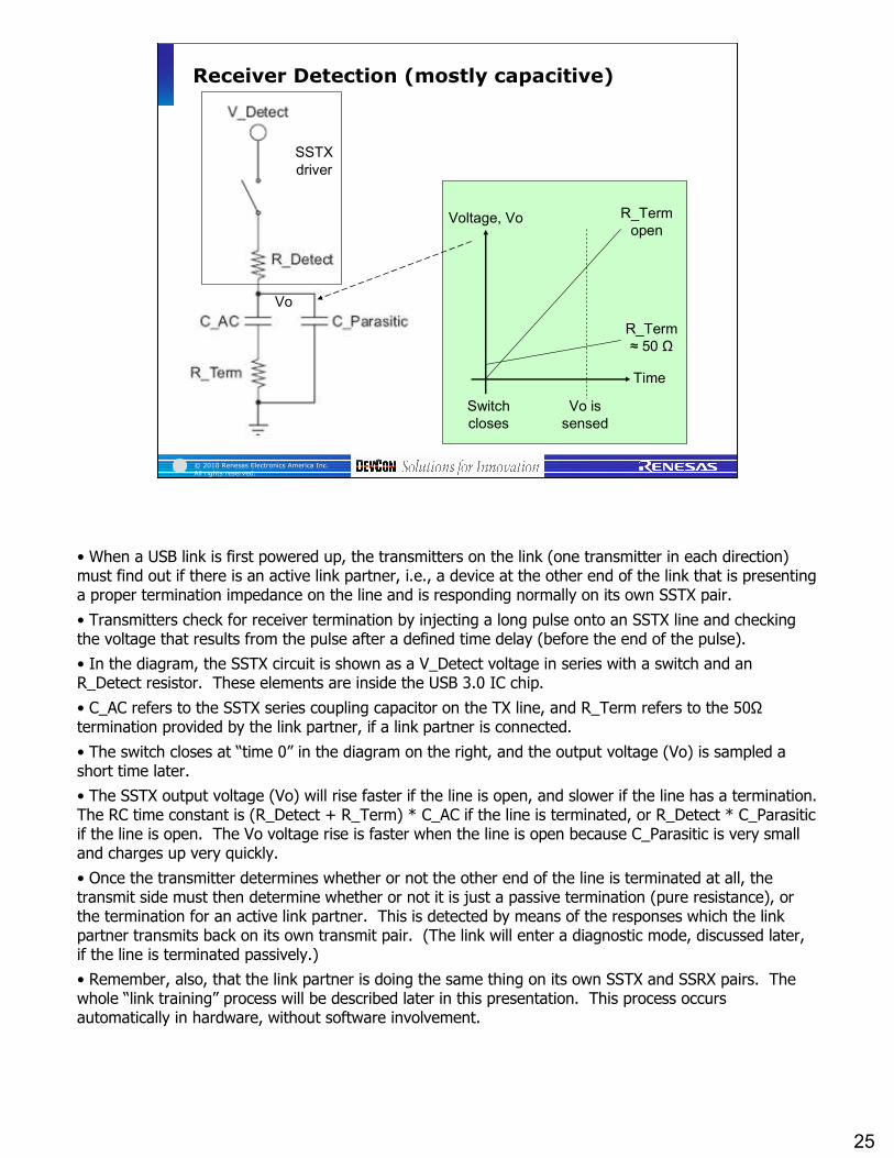
• When a USB link is first powered up, the transmitters on the link (one transmitter in each direction) must find out if there is an active link partner, i.e., a device at the other end of the link that is presenting a proper termination impedance on the line and is responding normally on its own SSTX pair.
• Transmitters check for receiver termination by injecting a long pulse onto an SSTX line and checking the voltage that results from the pulse after a defined time delay (before the end of the pulse).
• In the diagram, the SSTX circuit is shown as a V_Detect voltage in series with a switch and an R_Detect resistor. These elements are inside the USB 3.0 IC chip.
• C_AC refers to the SSTX series coupling capacitor on the TX line, and R_Term refers to the 50Ωtermination provided by the link partner, if a link partner is connected.
• The switch closes at “time 0” in the diagram on the right, and the output voltage (Vo) is sampled a short time later.
• The SSTX output voltage (Vo) will rise faster if the line is open, and slower if the line has a termination. The RC time constant is (R_Detect + R_Term) * C_AC if the line is terminated, or R_Detect * C_Parasitic if the line is open. The Vo voltage rise is faster when the line is open because C_Parasitic is very small and charges up very quickly.
• Once the transmitter determines whether or not the other end of the line is terminated at all, the transmit side must then determine whether or not it is just a passive termination (pure resistance), or the termination for an active link partner. This is detected by means of the responses which the link partner transmits back on its own transmit pair. (The link will enter a diagnostic mode, discussed later, if the line is terminated passively.)
• Remember, also, that the link partner is doing the same thing on its own SSTX and SSRX pairs. The whole “link training” process will be described later in this presentation. This process occurs automatically in hardware, without software involvement.

26
26 © 2010 Renesas Electronics America Inc. All rights reserved.
5 Gbps Electrical Signaling at Transmitter
Vo
lta
ge
(V
)
• This diagram shows the 5 Gbps signaling waveforms. The red trace is the single-ended SSTX+ signal, and the purple trace is the single-ended SSTX- signal.
• The black trace is the resulting differential voltage (Vtxp – Vtxn), referenced to 0v differential.
• The time scale is marked in units of 0.1 ns (100 ps). Each two marks constitute one UI for 5 Gbps signaling.
• The light green arrows show the differential voltage at the mid-UI points. The diagram shows a 1-to-0 transition bit, followed by two more ‘0’ bits, then a 0-to-1 transition bit followed by two more ‘1’ bits, and finally a 1-to-0 transition bit again.
• The transition bits are always full amplitude, while non-transition bits have a reduced amplitude, referred to as “de-emphasis.” The typical de-emphasis level in USB 3.0 is nominally -3.5 dB (a voltage reduction of 33%), but the de-emphasis actually shown in the diagram is closer to 50%.
• The differential signal should always be centered symmetrically around 0v, within a tolerance defined by the USB 3.0 Specification. The zero-crossings in the differential signal correspond to the points where Vtxp = Vtxn.
27
27 © 2010 Renesas Electronics America Inc. All rights reserved.
Signal at Receiver (after equalization)
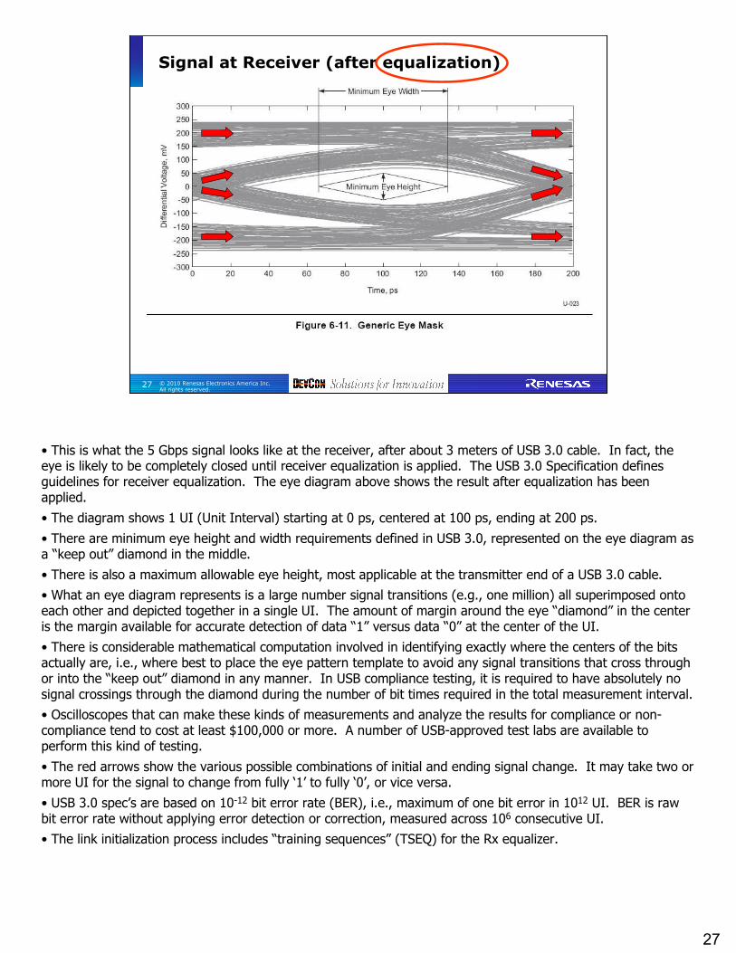
• This is what the 5 Gbps signal looks like at the receiver, after about 3 meters of USB 3.0 cable. In fact, the eye is likely to be completely closed until receiver equalization is applied. The USB 3.0 Specification defines guidelines for receiver equalization. The eye diagram above shows the result after equalization has been applied.
• The diagram shows 1 UI (Unit Interval) starting at 0 ps, centered at 100 ps, ending at 200 ps.
• There are minimum eye height and width requirements defined in USB 3.0, represented on the eye diagram as a “keep out” diamond in the middle.
• There is also a maximum allowable eye height, most applicable at the transmitter end of a USB 3.0 cable.
• What an eye diagram represents is a large number signal transitions (e.g., one million) all superimposed onto each other and depicted together in a single UI. The amount of margin around the eye “diamond” in the center is the margin available for accurate detection of data “1” versus data “0” at the center of the UI.
• There is considerable mathematical computation involved in identifying exactly where the centers of the bits actually are, i.e., where best to place the eye pattern template to avoid any signal transitions that cross through or into the “keep out” diamond in any manner. In USB compliance testing, it is required to have absolutely no signal crossings through the diamond during the number of bit times required in the total measurement interval.
• Oscilloscopes that can make these kinds of measurements and analyze the results for compliance or non-compliance tend to cost at least $100,000 or more. A number of USB-approved test labs are available to perform this kind of testing.
• The red arrows show the various possible combinations of initial and ending signal change. It may take two or more UI for the signal to change from fully ‘1’ to fully ‘0’, or vice versa.
• USB 3.0 spec’s are based on 10-12 bit error rate (BER), i.e., maximum of one bit error in 1012 UI. BER is raw bit error rate without applying error detection or correction, measured across 106 consecutive UI.
• The link initialization process includes “training sequences” (TSEQ) for the Rx equalizer.

28
28 © 2010 Renesas Electronics America Inc. All rights reserved.
3 12
5 Gbps Signals Need very Careful PCB Layout
• Top Layer: Signals
• 1st Inner Layer: GND plane
• 2nd Inner Layer: Split GND & Power
• Bottom Layer: Some 5 GHz signals
5
4
• This is a picture of the top layer (component side) of the Renesas EC34 ExpressCard (evaluation design) for the µPD720200. The card-edge connecter (“Gold fingers”) at the far right are designed to mate with the PCI Express bus in a laptop PC operating at either 2.5 Gbps or 5 Gbps (one lane). The card then provides two USB 3.0 ports via connectors shown on the left side of the card. The µPD720200 VLSI chip is mounted in the center of the card.
• The card has four layers, used as indicated in the slide.
• All 5 GHz signals for USB 3.0 and PCI Express are routed on the top and bottom layers (mostly on top). A continuous GND plane is required on the nearest inner layer. For the bottom layer, the corresponding GND plane covers only the areas needed by the 5 GHz signals, leaving other areas of the 2nd inner layer available for power routing.
• 5 GHz differential pairs require corresponding differential pair routing (1), careful routing through an ESD protection device (2), if used, and symmetrical routing through the AC coupling capacitors (3, for SSTX and PCIe Tx pairs).
• In this layout, there is a short route on the bottom of the board for the SSRX pairs near the USB 3.0 connectors. The SSRX pairs then go through vias to the top layer (4) to finish the path to the µPD720200.
• USB 3.0 SS and PCIe differential pairs require extremely close length matching of the traces in the pair, to within 5 mils (0.005 inch). This layout achieves length matching by using “serpentine” routing (5) near the µPD720200 pins.

29
29 © 2010 Renesas Electronics America Inc. All rights reserved.
5 Gbps Uses 8b/10b Encoding & Bit Scrambling
500 MHz
5 GHzFor EMI reduction:
Scrambling
Spread-Spectrum Clocking (SSC)
• This diagram shows how 8-bit data bytes (D) and control codes (K) are transformed into 10-bit “symbols” for serial transmission on the SS link. First, D-codes (but not K-codes) are “scrambled,” i.e., mapped to another 8-bit code using a Cyclic Redundancy Checksum (CRC) algorithm.
• Then 8b/10b encoding is applied to map the 8-bit code into a 10-bit symbol, followed by parallel-to-serial conversion and serial differential transmission.
• The reason for scrambling D-codes is to make the data pattern look pseudo-random and thereby cut down on strong harmonics at specific frequencies (bad for EMI).
• For diagnostic purposes, there is provision to disable D-code scrambling if needed, but never in normal operation for data transfer.
• K-codes use additional bit sequences in the set of 1024 possible 10-bit symbol codes and thus never duplicate the symbols for any 8-bit D-codes.
• For further EMI reduction, Spread-Spectrum Clocking (SSC) is described in the USB 3.0 Specification. This refers to modulating the 5 GHz bit clock slightly, from 0 to -5000 ppm, at a rate of 30 KHz to 33 KHz. SSC modulation is slow enough not to disrupt 5 Gbps operation, yet great enough to spread the frequency peaks that appear in a spectrum analysis of the radiated RF energy, so that the RF energy is somewhat more evenly distributed.

30
30 © 2010 Renesas Electronics America Inc. All rights reserved.
D-Code Examples
yyyxxxxx (binary)Dx.y
• Here are some examples of how D-codes are mapped to 10-bit symbols. This is an excerpt from the complete list of 256 D-code mappings, from Appendix A in the USB 3.0 Specification.
• The 10-bit symbols always have 4 one’s, 5 one’s, or 6 one’s. The number of one’s is important to maintain the DC balance needed with AC coupling. Remember that in USB 3.0, the 5 Gbps differential pairs are AC coupled. This is shown on a previous slide.
• The running DC imbalance is referred to as the “Running Disparity (RD)”. The disparity can be either “-” or “+”. There are two possible 10-bit symbols for each 8-bit D-code. One mapping compensates for “RD-”, while the other compensates for “RD+”. Even mappings with 5 one’s may have alternate mappings that still have 5 one’s.
• For example, D3.0 has two possible mappings. The RD- mapping has 6 one’s, while the RD+ mapping has 4 one’s.
• D0.0, D1.0 and D2.0 have two different mappings that both have 5 one’s.
• It may be tempting to assume that the alternate mapping for any symbol is just the one’s complement of the main mapping. But then we find cases like D3.0, D5.0 and D6.0 where that rule does not hold.
• D-codes and K-codes are denoted as “Dx.y” and “Kx.y,” where ‘x’ is the decimal value of the low-order 5 bits of the 8-bit code, and ‘y’ is the decimal value of the high-order 3 bits.
31
31 © 2010 Renesas Electronics America Inc. All rights reserved.
K-Codes
K28.7: Compliance & Loopback
K28.0: ReservedKx.y = yyyxxxxx
(binary)
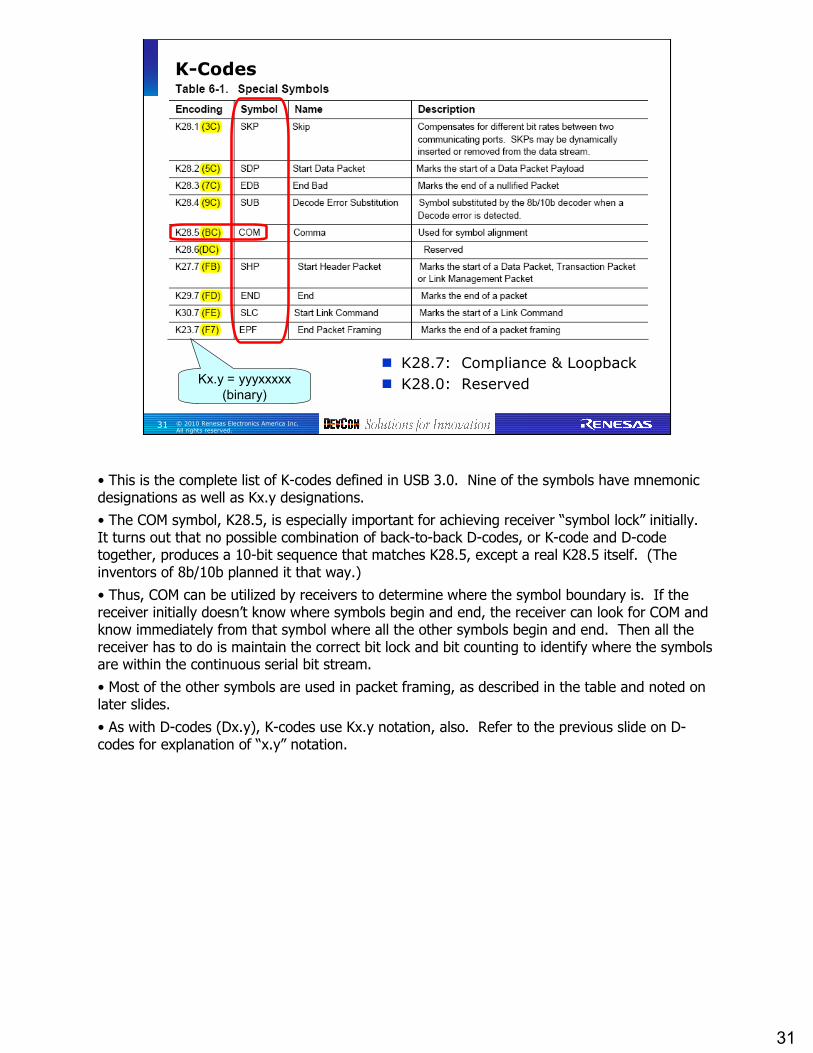
• This is the complete list of K-codes defined in USB 3.0. Nine of the symbols have mnemonic designations as well as Kx.y designations.
• The COM symbol, K28.5, is especially important for achieving receiver “symbol lock” initially. It turns out that no possible combination of back-to-back D-codes, or K-code and D-code together, produces a 10-bit sequence that matches K28.5, except a real K28.5 itself. (The inventors of 8b/10b planned it that way.)
• Thus, COM can be utilized by receivers to determine where the symbol boundary is. If the receiver initially doesn’t know where symbols begin and end, the receiver can look for COM and know immediately from that symbol where all the other symbols begin and end. Then all the receiver has to do is maintain the correct bit lock and bit counting to identify where the symbols are within the continuous serial bit stream.
• Most of the other symbols are used in packet framing, as described in the table and noted on later slides.
• As with D-codes (Dx.y), K-codes use Kx.y notation, also. Refer to the previous slide on D-codes for explanation of “x.y” notation.

32
32 © 2010 Renesas Electronics America Inc. All rights reserved.
Receiver Operations
Rx Equalization
Bit Clock Recovery
COM detection
for Symbol Lock
8b/10b Decode
Descrambling of D-codes
Buffering for clock
rate differences
• The job that must be done by a USB 3.0 SS receiver is significantly more complex than what the transmitter generates. First, the receiver usually can’t even determine where the bit boundaries are without applying equalization. The “eye pattern” at the receiver is likely to be completely closed (no identifiable “eye”) until after equalization. The USB 3.0 Specification discusses possible equalization approaches, but the ultimate decision is left to USB 3.0 implementers.
• Once the eye is opened up through equalization, the next problem is to find the best sampling point for the individual bits. This is the job of the Clock Recovery Circuit shown in the diagram. That clock then samples the equalized waveform to extract each bit.
• Note that the bit clocking is contained within the incoming bit stream. The stream is self-clocked. The number of transitions guaranteed in the 10-bit symbol codes is sufficient (after equalization) to convey the necessary bit clocking information for the receiver.
• It should also be noted that the whole process of clock recovery and bit extraction is extremely accurate. The bit error rate (BER) in USB 3.0 is only one bit error in a million-million bits (1012).
• After the bits are successfully extracted, the receiver must then search for a COM symbol (K28.5) to determine where the symbol boundaries are. This is actually done during the initial “Link Training” process, which will be described later in this presentation. After link training is completed, the receiver maintains the bit and symbol lock that was established during link training, and no further re-sync for bits and symbols is needed unless the link goes into a reduced power mode in which the 5 Gbps bit stream is shut off (i.e., Electrical Idle). The USB 3.0 Specification defines an orderly process for quickly retraining the link when it later comes out of the reduced power mode.

33
33 © 2010 Renesas Electronics America Inc. All rights reserved.
Receiver Operations
Rx Equalization
Bit Clock Recovery
COM detection
for Symbol Lock
8b/10b Decode
Descrambling of D-codes
Buffering for clock
rate differences
(Notes, continued)
• Receivers contain a small “Elastic Buffer” that is needed for clock rate compensation. By the time the symbols are being extracted, the clocking changes to a local clock in the receiver. The frequency of the local clock will be very close to the frequency of the clock embedded in the bit stream, but not quite exactly (and not frequency-locked to the incoming bit stream). Over time, the symbol clock rate mismatch can reach multiple symbol times. The combination of the elastic buffer and inserted or deleted SKP symbols in the data stream allows the clock rates to be matched. This is explained in more detail in the USB 3.0 Specification, along with precise limits on how much clock rate mismatch is allowed.
• Coming out of the elastic buffer, the symbols are then converted back to 8-bit values (8b/10b decoding) and (for D-codes) descrambled.
• Note that even during Logical Idle (D0.0 between packets, described later), the descrambler in the receiver must remain in sync with the scrambler in the transmitter. Otherwise, the 8-bit values extracted by the receiver will be unintelligible. This synchronization is achieved simply staying in sync (through UI counting) after the initial link training process.
• Link retraining can occur if needed to re-establish bit and symbol lock. The link training handshakes aredescribed later.

34
34 © 2010 Renesas Electronics America Inc. All rights reserved.
Big Picture: Types of Link Activity
Electrical Idle
Low Frequency
Periodic
Signaling
(LFPS)
Training
Sequences
(5 Gbps)
Logical idle
(5 Gbps)
• Data Packet Header & Payload (DPH, DPP)
• Transaction Packets (TP)
• Isochronous Timestamp Packets (ITP)
• Link Management Packets (LMP)
• Link Command Packets
Packets (5 Gbps)
Reset
Pow
er S
avin
g
Diagnostic
Sequences
(5 Gbps)
• Returning to the “Big Picture” of Link Activity, the next major topics are the Link Training sequences and Diagnostic Sequences.
• Link reset will also be described briefly.

35
35 © 2010 Renesas Electronics America Inc. All rights reserved.
TSEQ Format (scrambling disabled)
• There are three different Link Training Sequences: TSEQ, TS1, and TS2.
• They are referred to as “Ordered Sets,” although the significance of this terminology is a little unclear for a single differential pair. (With multiple lanes, such as in PCI Express, Ordered Sets refer to sequences sent on each lane separately rather than multiplexed across all the lanes.)
• TSEQ is the first Training Sequence that a link partner must send upon detecting a termination on the other end of the link.
• TSEQ is used by the link partner to establish its receiver equalization. TSEQ consists of a COM symbol (K28.5), followed by the specific sequence of D-codes listed in the table.
• TSEQ is transmitted repeatedly for a total of 65,536 repetitions.

36
36 © 2010 Renesas Electronics America Inc. All rights reserved.
TS1 and TS2 Formats (scrambling disabled)
• After receiver equalization is established, the next step in the link training process is for the link partners to begin sending TS1 Ordered Sets.
• Upon detecting TS1’s received in response to TS1’s transmitted, the transmitter begins sending TS2’s instead of TS1’s. The link partner is supposed to respond with TS2’s in return.
• It doesn’t matter which partner sees TS1 or TS2 first. The handshake is successfully completed when both partners are sending TS2 and seeing TS2 in return.
• Note that both of these Ordered Sets, like TSEQ, begin with a COM symbol. That symbol uniquely identifies the symbol boundary for the receiver.
• Once symbol lock is established in a receiver, the receiver maintains the lock by remaining in sync with the individual UI in the bit stream. This can continue indefinitely until the 5 Gbps bit stream is subsequently interrupted by a power management event.
• The meaning of Symbol 5 in TS1 and TS2 is shown on the next slide.

37
37 © 2010 Renesas Electronics America Inc. All rights reserved.
Link Configuration Field in TS1 and TS2
Note:
USB 3.0 supports SS lane polarity inversion.
Inversion is detected automatically via D10.2 during TSEQ or TS1 and TS2.
• Symbol 5 in TS1 and TS2 is a Link Configuration field. This slide shows the meaning of the 8 data bits in the decoded symbol #5 (D-code).
• Bit 0 signifies whether the TS1 or TS2 is a normal training sequence or a Hot Reset request. Hot Reset is one of several ways to reset a USB 3.0 SS link.
• Bit 2 enables Loopback mode, which is used for Bit Error Rate (BER) testing.
• It is also possible to disable data byte scrambling for test purposes. Bit 3 performs that function.
• USB 3.0 also supports lane polarity inversion (as does PCI Express). Polarity inversion means that the “+” and “-” lines in a differential pair are swapped. By checking the ending D-code in a TSEQ, TS1 or TS2, a receiver can determine if there is a +/- swap, and always swap the lines from then on until the next link training process.
• Automatic lane polarity detection may help to alleviate board layout constraints and avoid additional vias and crossovers on 5 GHz differential pairs.

38
38 © 2010 Renesas Electronics America Inc. All rights reserved.
Types of Link Reset
Power-On Reset
Self-powered device
Bus-powered device
Inband reset
Hot Reset: TS2
Warm Reset: LFPS
• USB 3.0 defines several modes of link and device reset.
• Some of the details of the required responses to reset depend on the type of reset.

39
39 © 2010 Renesas Electronics America Inc. All rights reserved.
Compliance Mode
CP0 CP1 … CP8Entry ResetPing.LFPS
Reset
• Compliance Mode allows link electrical compliance testing.
• This mode is entered automatically if there is a passive line termination on SS Tx but no active link partner responding on SS Rx. The timeout interval for detecting a link partner is 360 ms.
• There are actually 9 different Compliance patterns defined in USB 3.0, denoted as CP0 through CP8. A port in this mode steps through each pattern in response to a Ping.LFPS event transmitted by the de facto “link partner.” The Link Partner in this case is usually a USB-IF compliance test board having the ability to generate LFPS bursts for CP0-8 pattern stepping.
• The only way to exit from Compliance mode is by a link reset.
• The CP0 pattern, in particular, is intended specifically for eye pattern testing. It is just Logical Idle (D0.0 symbols sent continuously) without SKP symbols. (Because of bit scrambling, D0.0 sent repetitively will result in a pseudo-random pattern on the link.

40
40 © 2010 Renesas Electronics America Inc. All rights reserved.
Big Picture: Types of Link Activity
Electrical Idle
Low Frequency
Periodic
Signaling
(LFPS)
Training
Sequences
(5 Gbps)
Logical idle
(5 Gbps)
• Data Packet Header & Payload (DPH, DPP)
• Transaction Packets (TP)
• Isochronous Timestamp Packets (ITP)
• Link Management Packets (LMP)
• Link Command Packets
Packets (5 Gbps)
Reset
Pow
er S
avin
g
Diagnostic
Sequences
(5 Gbps)
• After the link is fully operational in 5 Gbps mode, it goes into Logical Idle. As already noted, Logical Idle is just the D0.0 symbol sent over and over (continuously). Because of D-code scrambling, the actual raw bit sequence on the link will be a pseudo-random pattern.
• This mode of link activity is referred to as the U0 power state.
• In this mode, the link is ready to transmit information packets as needed. The various possible packet types are listed in the diagram. The most important types for data transfer are DPH, DPP, and TP. These are discussed in more detail on subsequent slides.
• The details of ITP, LMP and Link Command Packets are beyond the scope of this presentation, although some additional information about them is provided in the Appendix. As their name implies, LMP and Link Commands pertain to link management, and ITP is used as a timing marker for Isochronous transfers such as video and audio streams.

41
41 © 2010 Renesas Electronics America Inc. All rights reserved.
Big Picture: 5 Gbps Symbol Sequences
Logical Idle
Training Sequences: TSEQ, TS1, TS2
Header Packets: DPH, TP, ITP, LMP
Data Packets: DPH + DPP
Link Command Packets:
LGOOD, LBAD, LRTY, LCRD
LGO, LAU, LXU, LPMA, LUP
• Continuing the “Big Picture” view of USB 3.0 SS link operation, here is a summary listing of all the types of symbol sequences in 5 Gbps mode.
• Logical Idle and the Training Sequences have already been discussed.
• The various types of Link Commands have the following meanings:
• LGOOD – Link Good
• LBAD – Link Bad
• LRTY – Link Retry
• LCRD – Link Credit (space available for subsequent packets)
• LGO – Request to enter a different power state
• LAU – Acknowledgement for previous LGO
• LXU – Rejection of previous LGO
• LPMA – Link Power Management ACK (previous LGO completed)
• LUP – Link Up, i.e., notification that the sender is in U0
• The next major topic will be Header Packets, focusing on DPH and TP, and Data Packets (DPH + DPP).

42
42 © 2010 Renesas Electronics America Inc. All rights reserved.
Header Packets
• All Header Packets have the same basic format as shown in the diagram, always 20 symbols.
• These packet diagrams show the symbols in MSB-to-LSB order from left to right, but the order of transmission on the link is always LSB first, i.e., from right to left (LSB to MSB).
• Header Packets always begin with four K-codes: three SHP (Start Header Packet) and one EPF (End Packet Format).
• 12 D-codes of information come next, followed by a 2-symbol checksum (CRC).
• The header packet ends with a Link Control Word consisting of two more D-codes. The Link Control Word provides further low-level control of the link.

43
43 © 2010 Renesas Electronics America Inc. All rights reserved.
Packet Header (in a Header Packet)
LMP
TP
DPH
ITP
• Here is a more detailed view of the 14-byte “Packet Header” in a 20-symbol “Header Packet.”
• The basic Header Packet format is used for four different kinds of packets, known as LMP, TP, DPH, and ITP.
• DPH and TP are the main “workhorse” packet types for data transfer. DPH (Data Packet Header) defines the start of a Data Packet, and TP (Transaction Packets) provide acknowledgements and requests for Data Packets.

44
44 © 2010 Renesas Electronics America Inc. All rights reserved.
Data Packet = DPH followed by DPP
• Finally we come to some real data payload. This is the ultimate prize in the whole elaborate USB 3.0 packet scheme.
• USB 3.0 defines a “Data Packet” as consisting of a Data Packet Header (DPH) followed immediately by a second packet identified as a “Data Packet Payload (DPP)”.
• The DPP, in turn, is mostly data, up to 1024 bytes of data, along with a 4-byte CRC checksum and a few symbols of packet header and packet ending. (Total of 12 symbols of DPP overhead for 1024 symbols of real data.)
• Note that DPP needs K-code symbols for the packet ending because it is variable length. The DPH needs no end-of-packet K-codes because it is fixed length.
• The DPH and DPP are separate packet types, but they are supposed to be sent together, back-to-back, with no Logical Idle interval or other packet traffic separating them.
• SHP and EPF symbols were shown on the DPH format slide. SDP and END are new with the DPP format. SDP means “Start Data Packet,” and “END” means “End of Packet.”
• There is also an “EDB” symbol that can be used at the end of a DPP to signify that the packet has been found to contain an error and should be considered invalid. “EDB” stands for “End Bad.” A USB 3.0 hub can change an END symbol into EDB if the hub detects a problem with the DPP. (Hubs don’t have enough local storage to buffer and entire DPP, but they can perform basic error checking “on the fly.”)
45
45 © 2010 Renesas Electronics America Inc. All rights reserved.
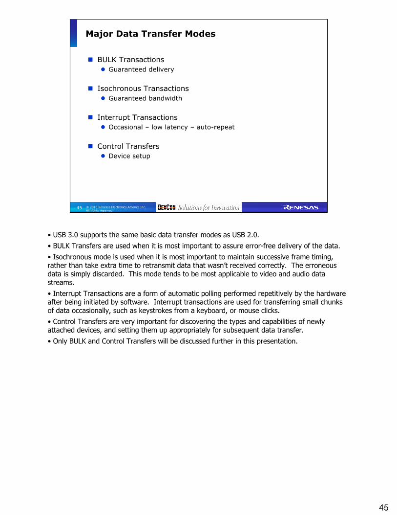
Major Data Transfer Modes
BULK Transactions
Guaranteed delivery
Isochronous Transactions
Guaranteed bandwidth
Interrupt Transactions
Occasional – low latency – auto-repeat
Control Transfers
Device setup
• USB 3.0 supports the same basic data transfer modes as USB 2.0.
• BULK Transfers are used when it is most important to assure error-free delivery of the data.
• Isochronous mode is used when it is most important to maintain successive frame timing, rather than take extra time to retransmit data that wasn’t received correctly. The erroneous data is simply discarded. This mode tends to be most applicable to video and audio data streams.
• Interrupt Transactions are a form of automatic polling performed repetitively by the hardware after being initiated by software. Interrupt transactions are used for transferring small chunks of data occasionally, such as keystrokes from a keyboard, or mouse clicks.
• Control Transfers are very important for discovering the types and capabilities of newly attached devices, and setting them up appropriately for subsequent data transfer.
• Only BULK and Control Transfers will be discussed further in this presentation.

46
46 © 2010 Renesas Electronics America Inc. All rights reserved.
Basic BULK IN Protocol (if no errors)
Figure 8-26: Sample BULK IN Sequence (excerpt)
Transaction
Packets (TP)
• BULK IN transactions allow data to be sent by a device to a host, in response to requests from the host.
• The protocol begins with the host sending an “IN” Transaction Packet (TP), also known as “IN (ACK).” The target device then responds with a data packet if available, or an error notification via a response TP.
• The next “IN (ACK)” TP sent by the host performs two purposes with a single TP: itacknowledges successful receipt of the previous data packet, and also requests the next data packet. Most TP types are actually variations on the ACK TP format.
• One of the fields in both TP and DPH packets is the packet Sequence Number, Seq. This field allows missing packets to be detected quickly.
• The “4” for the ACK(IN) packets in the diagram is not clearly explained in the USB 3.0 Specification, but it may refer to the NumP field in the ACK packet. NumP is described later in this presentation.
47
47 © 2010 Renesas Electronics America Inc. All rights reserved.
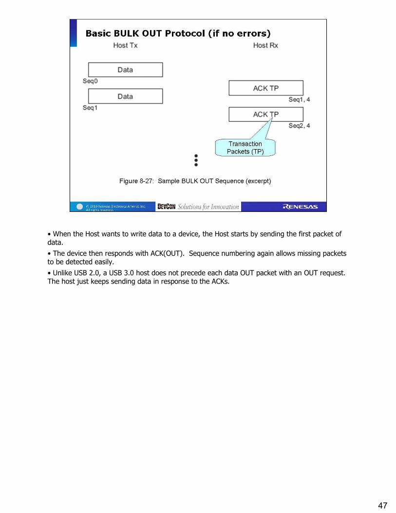
Basic BULK OUT Protocol (if no errors)
Figure 8-27: Sample BULK OUT Sequence (excerpt)
Transaction
Packets (TP)
• When the Host wants to write data to a device, the Host starts by sending the first packet of data.
• The device then responds with ACK(OUT). Sequence numbering again allows missing packets to be detected easily.
• Unlike USB 2.0, a USB 3.0 host does not precede each data OUT packet with an OUT request. The host just keeps sending data in response to the ACKs.

48
48 © 2010 Renesas Electronics America Inc. All rights reserved.
Data Packet Bursts
Multiple data packets back-to-back
NumP in ACK
Short packet
DPH
DPP
DPH
DPP
DPH
DPP
DPH
DPP
DPH
DPPACK
ACK
ACK
ACK
1
2
3
4
5
1
2
3
4
Host Tx Host Rx
• In the previous examples, no further data is transmitted until an ACK is received for the previous data packet.
• This means that each direction of the line has to sit idle while waiting for the ACK.
• Increased link utilization efficiency is possible if the sending of data doesn’t have to wait for a preceding ACK.
• USB 3.0 defines an orderly way to send data packets back-to-back without the delay of waiting for ACK after each data packet.
• The ACK packet format contains a field (NumP) that specifies how many data packets can be accepted in a burst, before waiting for all the ACK packets to come back.
• The best efficiency is achieved when the number of allowable data packets in a burst is great enough so that the ACK for the first packet will normally come back before the end of the burst, and a new burst can begin immediately upon finishing the previous burst. The link traffic for the data will then consist entirely of the data packets, one after the other, with no required delay between bursts or between packets within a burst.
• This method of data bursting is new in USB 3.0, as compared to USB 2.0, and is made possible by the fact that the link has separate transmit and receive paths. Transmitting can occur simultaneously with ACK responses, since there is no need to turn the link around (as with a bidirectional link) to allow the responses.
• Within a data transfer, each packet except the last is required to be maximum size (1024 bytes). A “short packet” is assumed to be the final packet in the transfer.
• There is also a length parameter in the packet format, and it is an error for the short packet to occur too soon or too late compared to the packet length defined by the length parameter.
• In Bulk protocol, packet errors typically result in subsequent retries.

49
49 © 2010 Renesas Electronics America Inc. All rights reserved.
Performance Analysis
Sources of performance overhead
Raw bit rate: 5 Gbps
After 8b/10b decoding: 500 MB/sec
80% of 5 Gbps
Data packets (DPH + DPP):
32 symbols for 1024 data bytes
Lose 3% of 500 MB/sec
SKP symbols
Idle time between packets
Often HUGE
Use burst mode
Can the source & sink achieve 500 MB/sec?
Actual testing
25 GB in 70 sec = 357 MB/sec
71% of 500 MB/sec
• From the foregoing explanation of how data payloads are packaged and transmitted, some basic link performance parameters can be estimated.
• Overheads (link utilization inefficiencies) can come from a number of sources, as shown in the slide.
• 8b/10b encoding, in particular, reduces effective link utilization efficiency to 80% of 5 Gbps, i.e., 500 MB/sec.
• Packet formatting and other overheads reduce effective link utilization still further, roughly 3% of 500 MB/sec.
• Perhaps the greatest source of inefficiency in most systems will be the idle time between successive data packets in a transfer. The key to reducing that delay is to use burst mode effectively.
• After all of the various overheads are allowed for, the resulting transfer efficiency has been measured at around 350 MB/sec, to transfer a 25 GB movie file in only 70 seconds. That is more than 10 times faster than the 14 minutes needed to transfer the same movie file using USB 2.0. (14 x 60 / 70 = 12.)
• To avoid confusion over whether 1 KB is 1000 bytes or 1024 bytes, some manufacturers use the following alternative terms established by the IEC:
• 1 KiB = 1 Kibibyte = 210 bytes = 1024 bytes = 1.02 KB (approx)
• 1 MiB = 1 Mebibyte = 220 bytes = 1.05 MB (approx)
• 1 GiB = 1 Gibibyte = 230 bytes = 1.07 GB (approx)
• 1 TiB = 1 Tebibyte = 240 bytes = 1.10 TB (approx)
• The “bi” in these terms refers to “binary,” i.e., power of 2. USB 3.0 and this presentation do not use these terms, but you may encounter them in the industry.

50
50 © 2010 Renesas Electronics America Inc. All rights reserved.
Performance Analysis
Sources of performance overhead
Raw bit rate: 5 Gbps
After 8b/10b encoding: 500 MB/sec
80% of 5 Gbps
Data packets (DPH + DPP):
32 symbols for 1024 data bytes
Lose 3% of 500 MB/sec
SKP symbols
Idle time between packets
Often HUGE
Use burst mode
Can the source & sink achieve 500 MB/sec?
Actual testing
25 GB in 70 sec = 357 MB/sec
71% of 500 MB/sec
(Notes, continued)
• It should also be noted that benchmark measurements such as 350 MB/sec refer to a single data stream not in contention with any other streams in the system during the test. The benchmark picture becomes considerably more complicated when two or more streams are being benchmarked simultaneously. At worst, the total throughput of both streams together would be expected to equal 350 MB/sec, but the actual results are often far better than that because of the way the various overheads for each stream might overlap each other. The total throughput for multiple devices together can often be greater than the highest throughput attainable by one device alone. In other words, just as an example, one device alone might achieve 350 MB/sec, and each might be reduced to 200 MB/sec when operated together, resulting a total of 400 MB/sec instead of 350 MB/sec. It’s impossible to give general rules about this, however, because there are so many variables involved in the characteristics of individual devices, host controllers, and software drivers and application programs.
• Probably a more common scenario would be that an individual device might top out at around 200 MB/sec by itself, and decline to 175 MB/sec when operated simultaneously with a second device of the same type, but both devices together might achieve a total combined throughput of 350 MB/sec.
• A protocol analyzer probably would be needed to identify exactly where the performance-degrading overheads are.
51
51 © 2010 Renesas Electronics America Inc. All rights reserved.
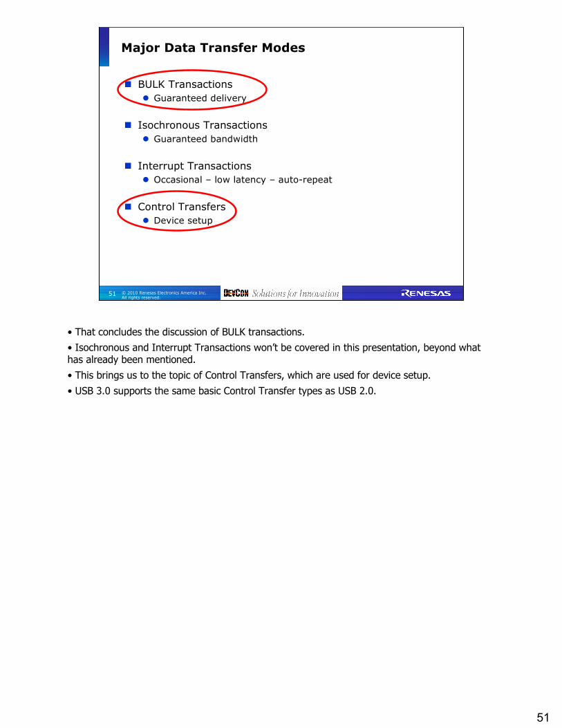
Major Data Transfer Modes
BULK Transactions
Guaranteed delivery
Isochronous Transactions
Guaranteed bandwidth
Interrupt Transactions
Occasional – low latency – auto-repeat
Control Transfers
Device setup
• That concludes the discussion of BULK transactions.
• Isochronous and Interrupt Transactions won’t be covered in this presentation, beyond what has already been mentioned.
• This brings us to the topic of Control Transfers, which are used for device setup.
• USB 3.0 supports the same basic Control Transfer types as USB 2.0.

52
52 © 2010 Renesas Electronics America Inc. All rights reserved.
Control Transfer: Read
Setup &
ACK
IN (ACK) &
Read Data
1 or more
STATUS
& ACK
Example: Get Device Descriptor
DPH + DPP
• Control Transfers are needed before data transfer can occur on a USB link, to determine device type and capabilities, and to initialize it for data transfer.
• A Control Transfer in USB 3.0 begins with a data packet with the ‘S’ bit set to ‘1’ in the DPH. This signifies that the DPH is a SETUP packet.
• The SETUP DPH is accompanied by a DPP that contains information about the type of Control Transfer to be performed. (Like all data packets, a SETUP data packet consists of a DPH and a DPP back-to-back.)
• Control Read Transfers are used to transfer data about a device to the host, and Control Write Transfers are used to program the device. The read or write data, if needed, is transferred during the Data Stage of the Control Transfer, consisting of one or more data packets.
• A STATUS packet then terminates the Control Transfer. STATUS is a type of Transaction Packet (TP).
• One example of a Control Read Transfer is the “Get Device Descriptor” command.
• Every device usually has multiple “endpoints,” with endpoint 0 always devoted to control of the device itself.Control Transfers are always directed to endpoint 0 in the target device.
• Every DPH and the final STATUS packet in a Control Transfer require a corresponding ACK.
•In the other direction, Control Write Transfers can program the contents of various writeable “descriptors” in the target device.
•As with normal data packets, each packet in a Control Transfer requires a corresponding ACK from the recipient of the packet. Most packets are sent by the Host, and the target device sends ACK (if there are no errors detected). For Control Read Transfers, the device sends the requested data, and the Host sends the ACK back to the device.
•As with BULK data packet transactions, the “1” and “0” in “Seq3, 1” and “Seq4, 0” (etc.) are not clearly explained in the USB 3.0 Specification, but they may refer to the NumP field in the ACK packet format.
Control Transfers prepare a device for subsequent data transfer activity.
Control Transfers are always directed to Endpoint 0 in the target device.
This is the same concept as in USB 2.0, but with very different packet formatting.
Control Transfers begin with a SETUP TP, optionally followed by one or more Data Packets (DP), and always terminated by a STATUS TP.
A SETUP packet is just a Data Packet with “S” bit set to ‘1’.
Data Packets can be Out from the host (Control Write) or In to the host (Control Read).
Each packet requires an ACK TP from the device (or from the host for data packets which the host receives from the device).

53
53 © 2010 Renesas Electronics America Inc. All rights reserved.
Control Transfer: Write
Setup &
ACK
STATUS
& ACK
Write Data
& ACK
0 or more
Example: Set Device Address
DPH + DPP
• This slide shows the general Control Write Transfer protocol.
• Initially, when a device or hub is first attached to another hub or Root Hub, hardware in the upstream hub or Host automatically detects the attachment and alerts the Host software.
• The Host then performs a series of Control Transfers to find out what kind of device has been attached (by reading the “descriptors” in the device).
• The Host then programs the device as needed to get it ready for further activity such as file reading or writing or other operations.
• One of the first Control Write Transfers which the Host must perform is the “Set Device Address” command (also known as a “USB Request”). Initially upon attachment, the device will automatically have a device address of 0. The host is notified by a port status register that an attachment has occurred, and the host has the ability to enable or disable the specific hub or host USB port for the new device. The Host uses device address 0 initially after enabling the port to which the device is attached, but the Host needs to set a nonzero device address very early in the enumeration process so that the device can be accessed uniquely without interference with any other devices that will also initially be set to address 0 as soon as their ports are enabled.
• Any configuration setup needed by a device must be completed during these enumeration Control Transfers. Any text ID “strings” stored in the device will also be read by the Host and displayed as needed for the benefit of users.
• Each endpoint in the device will need setup, too, using Control Transfers.
• For simple commands that don’t need much write data, the necessary information is part of the SETUP packet, and no subsequent data packets are needed (no “data stage”).

54
54 © 2010 Renesas Electronics America Inc. All rights reserved.
Question
Question 2: How fast is USB 3.0?
Answer 2: 5 Gbps in Super Speed (SS).
10X faster than USB 2.0 (HS).
350 MB/sec measured for SS so far.

55
55 © 2010 Renesas Electronics America Inc. All rights reserved.
Additional Considerations
What about software?
USB logo certification?
• We will conclude with a brief discussion of a few other topics, including USB software, followed by a live demo of a low-cost but versatile protocol analyzer.

56
56 © 2010 Renesas Electronics America Inc. All rights reserved.
USB Software
USB software is a major task
Host Controller driver
Additional “class drivers”
Device-specific drivers
USB 2.0 software today – PC & MCU
USB 3.0 software still very new, PC only
Can MCUs support SS transfer rates?
Mass storage peripherals for PCs
LucidPort USB300 ASIC
• USB software development is often a case of “Don’t try this yourself” – unless you have a substantial staff of experienced USB software engineers, or access to it.
• It’s probably not too big a task if your target application is very narrowly defined and you don’t need full compatibility with the whole range of possible USB 3.0 and USB 2.0 devices and hubs.
• Full compatibility depends on multiple layers of device drivers, including “class drivers” that relieve much of the burden of developing any additional, customized drivers needed for specific devices.
• And don’t forget the Host Controller. There needs to be one at the top of the hierarchy, and it needs a driver, too.
• So far, USB 3.0 hardware and software has been mostly PC-oriented. In time, however, we expect to see increasing uses for the speed of USB 3.0 in microcontroller applications, particularly as data sinks and sources for microcontrollers increase in data throughput capabilities. USB 3.0 should be considered for any situation where large amounts of data need to be moved from a high-speed source to a high-speed sink in far less time than is currently possible with USB 2.0.
• One current microcontroller-based application for USB 3.0 is in USB 3.0 mass storage devices, to coordinate SS data transfer between the USB 3.0 logic and the SATA hard disk drive logic. The LucidPort USB300 SATA bridge ASIC uses a USB 3.0 IP core from Renesas.
57
57 © 2010 Renesas Electronics America Inc. All rights reserved.
57
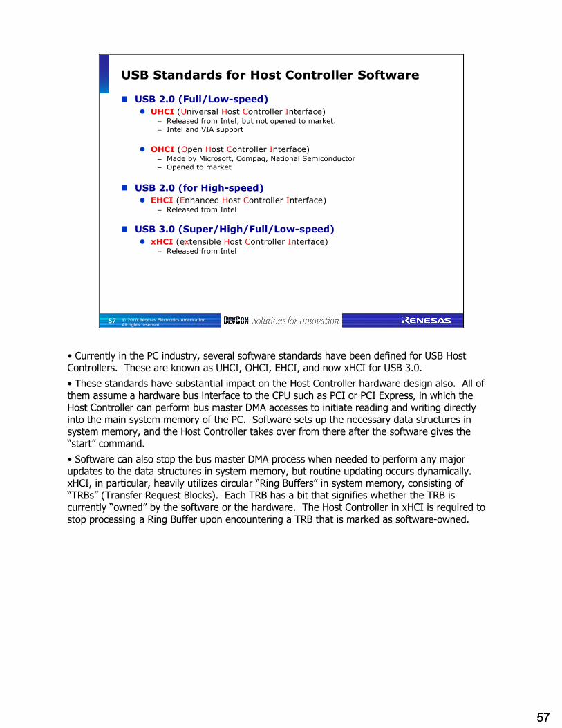
USB Standards for Host Controller Software
USB 2.0 (Full/Low-speed)
UHCI (Universal Host Controller Interface)– Released from Intel, but not opened to market.– Intel and VIA support
OHCI (Open Host Controller Interface)– Made by Microsoft, Compaq, National Semiconductor– Opened to market
USB 2.0 (for High-speed)
EHCI (Enhanced Host Controller Interface)– Released from Intel
USB 3.0 (Super/High/Full/Low-speed)
xHCI (extensible Host Controller Interface)– Released from Intel
• Currently in the PC industry, several software standards have been defined for USB Host Controllers. These are known as UHCI, OHCI, EHCI, and now xHCI for USB 3.0.
• These standards have substantial impact on the Host Controller hardware design also. All of them assume a hardware bus interface to the CPU such as PCI or PCI Express, in which the Host Controller can perform bus master DMA accesses to initiate reading and writing directly into the main system memory of the PC. Software sets up the necessary data structures in system memory, and the Host Controller takes over from there after the software gives the “start” command.
• Software can also stop the bus master DMA process when needed to perform any major updates to the data structures in system memory, but routine updating occurs dynamically. xHCI, in particular, heavily utilizes circular “Ring Buffers” in system memory, consisting of “TRBs” (Transfer Request Blocks). Each TRB has a bit that signifies whether the TRB is currently “owned” by the software or the hardware. The Host Controller in xHCI is required to stop processing a Ring Buffer upon encountering a TRB that is marked as software-owned.
57

58
58 © 2010 Renesas Electronics America Inc. All rights reserved.
USB 3.0 Hubs
Figure 10-1. Hub Architecture
SS
SSHS,FS,LS
HS,FS,LS
Upstream
(US) Port
Downstream
(DS) Ports
• USB 3.0 hubs are just beginning to become available in the market. This session will not discuss hubs in much detail, but additional information can be found in the USB 3.0 Specification, especially Chapter 10.
• USB 3.0 hubs contain two separate hubs internally, and two separate signal paths for each internal hub: SS path, and HS/FS/LS path.
• The two internal hubs and paths operate almost completely independently (and simultaneously), passing traffic of the appropriate speed as needed. The host sees two separate internal hubs and signal paths, also.
• Any speed of device can be connected to the hub. All communication with the device utilizes whichever internal path is appropriate for the speed for the target device.
• There is no transaction translator to translate SS packets on the upstream side into HS, FS or LS packets on the downstream side. Instead, the host uses whichever set of signals matches the speed of the device – SS signals for SS devices, or USB2 signals for USB2 devices. (USB 2.0 hubs need a transaction translator for HS to FS/LS because they use the same signals for all three speeds, and we don’t want to block HS traffic because of FS or LS traffic.)
• There is only one port power control mechanism for the downstream ports, regardless of port speed. If either the SS path or the HS/FS/LS path is requesting port power to be on, then power for the port is on (assuming that port power control is supported at all in the hub design; hubs can be designed to leave port power always on).
• Note that it is possible in a dual-path architecture such as this for SS packets to be initiated and/or completed while HS/FS/LS packets are still in process. The two signal paths are entirely independent (except for port power).

59
59 © 2010 Renesas Electronics America Inc. All rights reserved.
Route String in Header Packets (TP, DPH)
Point-to-Point vs. Broadcast
Route string specifies path
Hubs are told their hub depth
• USB 3.0 uses “point to point” protocol, meaning that most packets specify a particular target destination instead of being broadcast all devices in the topology. This is another link utilization improvement in USB 3.0, as compared to USB 2.0.
• The intended target for a packet can always be denoted by the Device Address of the target, but intermediate hubs have no way to know the device addresses of other devices existing in the hierarchy that is serviced by a given hub.
• To tell a hub how to route a packet, all Header Packets (except ITP) contain a “Route String” that specifies every successive hub exit port number. The packet enters the hub with a route string, which tells the hub which of its ports the packet should go to. The packet then exits the hub on the specified port of the hub.
• The hub knows which field in the route string to look at because of a “hub depth” parameter that is programmed into the hub during enumeration.
• The route string contains up to 5 hub exit port numbers, corresponding to the number of hub levels in the route.
• It is the responsibility of the Host Controller (Root Hub) to build proper route strings based on various tables set up during enumeration to describe what is connected to what in the topology.
• ITP (Isochronous Timestamp Packet) is broadcast to all devices and thus does not require a route string.
• If you examine a protocol analyzer capture and find that a packet is being directed to a totally wrong destination compared to the device address listed in the packet header, one possible cause to be checked is the setup of the master topology tables maintained by the Host (possible software issue, device not where it was expected to be).

60
60 © 2010 Renesas Electronics America Inc. All rights reserved.
Question
Question 3: When I plug a device into a USB port, I don’t get SS speed. How come?
Answer 3:
Maybe the host port is not a USB 3.0 port.
Maybe the cable is not a USB 3.0 cable.
Maybe the device is not USB 3.0 SS capable.
All three factors are needed to get USB 3.0 SS operation, even though the device remains fully usable in USB 2.0 mode if any one of the essential factors for SS is missing.
Also, if you have an external hub anywhere in your signal path, make sure it is USB 3.0 SS capable, too.
USB 2.0 still works well when the hub is limited to USB 2.0.
• This kind of question comes up often from end users.

61
61 © 2010 Renesas Electronics America Inc. All rights reserved.
USB-IF certification
There are two mechanisms for testing products to get them on the Integrators list (certification list)
Participate in the USB-IF Sponsored Compliance Workshops
Contact one of the USB-IF approved Independent Test Labs
Testing
Super-Speed, Full-Speed, and High-Speed Electrical Testing
Interoperability Testing
Functional Testing
Compliance with System Checklist
Additional info publicly available at: http://www.usb.org/developers/compliance/
61
• If you are designing a product that will need USB-IF certification and USB logo, you will need to submit it to the USB-IF certification process. This slide summarizes the main issues involved in certification.
• All of the USB logos shown at the bottom of the slide are owned by the USB-IF and cannot be used on a product without formal USB-IF certification and compliance. The ExpressCard logo is owned by another industry organization, PCMCIA.
• USB compliance testing generally consists of electrical, interoperability, functional, and compliance with the USB-IF System Checklist.
• The USB-IF periodically offers Compliance Workshops in different cities worldwide (most often U.S. and Asia), and approved independent test labs are available as well.
61

62
62 © 2010 Renesas Electronics America Inc. All rights reserved.
Demo ― USB 3.0 Protocol Analyzer
Analyzer by Total Phase, Inc., http://www.totalphase.com
Captures up to 2 GB of data at 5Gbps
Analysis software on a control PC
Priced under $10,000
• We are pleased to be able to present a live demonstration of the very new USB 5000 Protocol Analyzer from Total Phase.
• Total Phase is a familiar analyzer manufacturer at DevCon, offering other technical sessions on analyzers for other signaling technologies, including USB 2.0.
• The USB 5000 is one of their newest analyzers, targeted for USB 3.0.
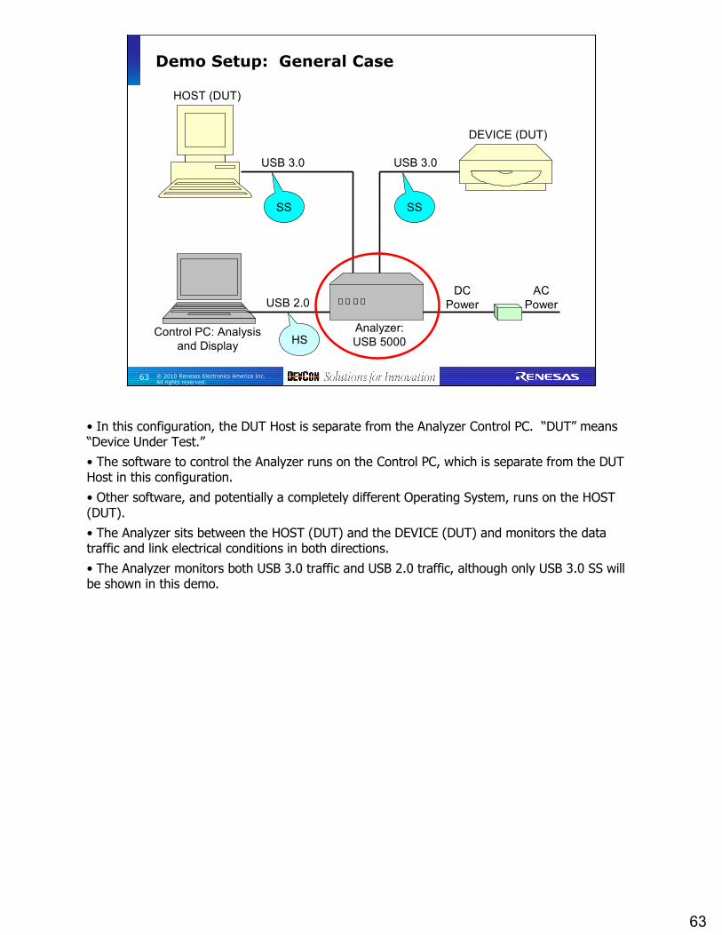
63
63 © 2010 Renesas Electronics America Inc. All rights reserved.
Demo Setup: General Case
USB 3.0 USB 3.0
USB 2.0DC
Power
AC
Power
HOST (DUT)
DEVICE (DUT)
SS SS
HSControl PC: Analysis
and Display
Analyzer:
USB 5000
• In this configuration, the DUT Host is separate from the Analyzer Control PC. “DUT” means “Device Under Test.”
• The software to control the Analyzer runs on the Control PC, which is separate from the DUT Host in this configuration.
• Other software, and potentially a completely different Operating System, runs on the HOST (DUT).
• The Analyzer sits between the HOST (DUT) and the DEVICE (DUT) and monitors the data traffic and link electrical conditions in both directions.
• The Analyzer monitors both USB 3.0 traffic and USB 2.0 traffic, although only USB 3.0 SS will be shown in this demo.
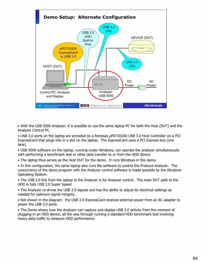
64
64 © 2010 Renesas Electronics America Inc. All rights reserved.
Demo Setup: Alternate Configuration
DC
Power
AC
Power
HOST (DUT)
DEVICE (DUT)
USB 3.0
(SS)USB 2.0
(HS)
Built-In
Port
Control PC: Analysis
and Display
Analyzer:
USB 5000
USB 3.0
(SS)
uPD720200
ExpressCard
to USB 3.0
• With the USB 5000 Analyzer, it is possible to use the same laptop PC for both the Host (DUT) and the Analyzer Control PC.
• USB 3.0 ports on the laptop are provided by a Renesas µPD720200 USB 3.0 Host Controller on a PCI ExpressCard that plugs into in a slot on the laptop. The ExpressCard uses a PCI Express bus (one lane).
• USB 5000 software on the laptop, running under Windows, can operate the analyzer simultaneously with performing a benchmark test or other data transfer to or from the HDD device.
• The laptop thus serves as the Host DUT for the demo. It runs Windows in this demo.
• In this configuration, the same laptop also runs the software to control the Protocol Analyzer. The concurrency of the demo program with the Analyzer control software is made possible by the Windows Operating System.
• The USB 2.0 link from the laptop to the Analyzer is for Analyzer control. The main DUT path to the HDD is fully USB 3.0 Super Speed.
• The Analyzer re-drives the USB 3.0 signals and has the ability to adjust its electrical settings as needed for optimum signal integrity.
• Not shown in the diagram: the USB 3.0 ExpressCard receives external power from an AC adapter to power the USB 3.0 ports.
• The Demo shows how the Analyzer can capture and display USB 3.0 activity from the moment of plugging in an HDD device, all the way through running a standard HDD benchmark test involving heavy data traffic to measure HDD performance.

65
65 © 2010 Renesas Electronics America Inc. All rights reserved.
Questions?
• General Q&A

66
66 © 2010 Renesas Electronics America Inc. All rights reserved.
Innovation: 10X Faster File Transfer
70 sec
HD Movie25 Gbyte
14 minutes for USB 2.0 HS
USB 3.0 is a great enabler for faster file transfers to and from mass storage devices and today’s modern handheld storage and display/communication devices. The slide shows the dramatic difference in speed between USB 2.0 and USB 3.0 for loading a 25 GB high-definition movie onto a portable storage and playback device. The less time a user has to spend waiting for such transfers, the happier the user will be. And the higher-definition movies that now become practical to transfer make users happier, as well, enriching their overall living experience.

67
67 © 2010 Renesas Electronics America Inc. All rights reserved.
Feedback Form
Please fill out the feedback form!
If you do not have one, please raise your hand
•
68
© 2010 Renesas Electronics America Inc. All rights reserved.
68
Thank You!
Welcome to DevCon 2010!
We hope you will enjoy the rest of the conference.

69
© 2010 Renesas Electronics America Inc. All rights reserved.
69
Appendix
• The remaining slides provide some additional technical information about various aspects of USB 3.0.

70
70 © 2010 Renesas Electronics America Inc. All rights reserved.
References for Further Information
USB 3.0 Specification, available from the USB Implementers Forum (USB-IF). Throughout this presentation, table numbers and diagram numbers have been preserved to allow the corresponding material in the USB 3.0 Specification to be located easily.
Unless otherwise noted, all table numbers and diagram numbers are from the USB 3.0 Specification.
USB 2.0 Specification, available from the USB-IF. USB 3.0 is backward compatible with USB 2.0 and retains many high-level concepts from USB 2.0.
By far the best source of technical details about USB 3.0 features and requirements is the official USB 3.0 Specification itself, from the USB-IF. Unfortunately, it is written as a reference document, not a tutorial textbook. Furthermore, USB 3.0 textbooks often tend to be a little too high-level, not providing the same level of detail that a user might need and would find in the USB 3.0 Specification. This presentation attempts to bridge that gap, focusing mainly on high-level topics, but also providing enough detail and especially references to the complete USB 3.0 Specification, so that attendees can find whatever additional detail they might need quickly and intelligibly.

71
71 © 2010 Renesas Electronics America Inc. All rights reserved.
SuperSpeed in market
P55-GD85
On M
B
On M
BOn M
B
All use Renesas’ USB 3.0 Host Controller!!
On M
B
ASUS GIGABYTE msi
U3S6
BUFFALORATOC
I/O Data
FujitsuRenesas Lenovo HP
Note: MB means Motherboard
On M
B
The Renesas µPD720200 device was the first USB 3.0 host controller in the market and the first to receive USB-IF certification. It has been used in all kinds of application so far, indicated in the slide. It provides a quick way for PC motherboard manufacturers to implement USB 3.0 ports on their PC’s without waiting for core logic providers to implement USB 3.0 in their chipsets. It can be used on add-in cards, both PCI Express cards for desktop PC’s and laptop ExpressCards, to give users an efficient path to USB 3.0 on PC’s that don’t provide USB 3.0 on their motherboards.
With USB 3.0 becoming more available on PC’s, USB 3.0 peripheral vendors have the opportunity to create the USB 3.0 peripherals that can take advantage of the higher speed of USB 3.0. Initial applications for USB 3.0 in peripherals include mass storage devices and video products, interfacing to PC’s through user-attached USB 3.0 connections. USB 3.0 finally offers data rates faster than current HDD technology, so that the USB link is no longer the limiting factor for throughput to and from those devices. USB 3.0 is even fast enough to keep up with the demands of high-performance video and graphics display applications, externally attached to the PC by USB 3.0 cable.
71

72
72 © 2010 Renesas Electronics America Inc. All rights reserved.
How much time can you save with USB 3.0?
Typical File Sizes
1GB 6GB 16GB 25GB
USB 1.1 22 mins. 2.2 hours 5.9 hours 9.3 hours
USB 2.0 33 secs. 3.3 mins. 8.9 mins. 14 mins.
USB 3.0 3 secs. 20 secs. 53 secs. 70 secs.
72
User tolerance for waiting for Sync-and–Go is
less than 90 secs.!
The biggest advantage of USB 3.0 is its speed improvement over USB 2.0 (480Mbs to 5Gbps). It’s 10 times faster than USB 2.0.
72
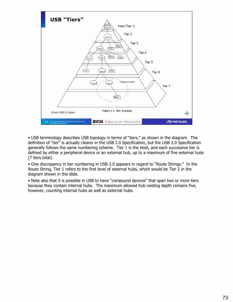
73
73 © 2010 Renesas Electronics America Inc. All rights reserved.
USB “Tiers”
(From USB 2.0 Spec)
• USB terminology describes USB topology in terms of “tiers,” as shown in the diagram. The definition of “tier” is actually clearer in the USB 2.0 Specification, but the USB 3.0 Specification generally follows the same numbering scheme. Tier 1 is the Host, and each successive tier is defined by either a peripheral device or an external hub, up to a maximum of five external hubs (7 tiers total).
• One discrepancy in tier numbering in USB 3.0 appears in regard to “Route Strings.” In the Route String, Tier 1 refers to the first level of external hubs, which would be Tier 2 in the diagram shown in the slide.
• Note also that it is possible in USB to have “compound devices” that span two or more tiers because they contain internal hubs. The maximum allowed hub nesting depth remains five, however, counting internal hubs as well as external hubs.

74
74 © 2010 Renesas Electronics America Inc. All rights reserved.
Standard-A Plug (cut away view)
USB 3.0
pins 5-9
USB 2.0
pins 1-4
This is the official “engineering diagram” of the Standard-A Plug, from the USB 3.0 Specification, Chapter 5.

75
75 © 2010 Renesas Electronics America Inc. All rights reserved.
Standard-A Receptacle
USB
3.0
pins
5-9
USB
2.0
pins
1-4
Pins
1 &
9 on
left
• This diagram shows the Standard-A Receptacle.
• Note that here the SS pins are near the front of the receptacle, to mate with the recessed SS pins in the Standard-A plug.
• The added SS pins are embedded into the main insulator block such that the USB 2.0 pins in the plug cannot make contact with the SS pins in the receptacle when the plug is inserted into the receptacle or pulled out. There is never an instant when SS pins are in contact with USB 2.0 pins.
• This slide also shows the pin numbering order.

76
76 © 2010 Renesas Electronics America Inc. All rights reserved.
USB 3.0 Standard-B Receptacle
For use on the
upstream-facing
port of a device or
hub.
Pins 1-4 are
standard USB 2.0.
Pins 5-9 are added
for USB 3.0.
Receptacle has a
total of 9 pins, plus
the shell for
shielding.
• The Standard-B Receptacle for USB 3.0 has an added section at the top for the five additional SS pins, in addition to the original four USB 2.0 pins.
• The design of the USB 2.0 section of this receptacle allows a USB 2.0 Standard-B plug to be inserted, allowing USB 2.0 cables and host/hub ports to connect to USB 3.0 peripheral devices and hubs.
• This diagram also shows the pin numbering order for the Standard-B receptacle.

77
77 © 2010 Renesas Electronics America Inc. All rights reserved.
Standard-A to Standard-B USB 3.0 Cable
• This is the formal USB 3.0 definition of the Standard-A to Standard-B cable.
• This would typically be used to connect a Host port (or hub) to a peripheral device (or hub).
• This table shows the two added SS GND wires in the cable both connecting to pin 7 on the USB 3.0 connectors on each end of the cable.
• Note that the original USB 2.0 GND wire in the cable connects only to pin 4 on both ends, but not to the other GND on pin 7.
• The main shield braid in the cable connects to the shell of each connector, but not to the pin 4 or 7 GND.
• On the Host end of the cable, pins 5 and 6 are the SS RX pair, but are the SS TX pair on the device end. The Host receives data from the device on this differential pair.
• Similarly, pins 8 and 9 are the SS TX pair on the Host end, but become SS RX on the device end. The Host transmits data to the device on this differential pair.
• It should also be noted that the VBUS pins and cable wire are specified to carry significantly more current in USB 3.0 than in USB 2.0, i.e., 900 mA max instead of 500 mA max.
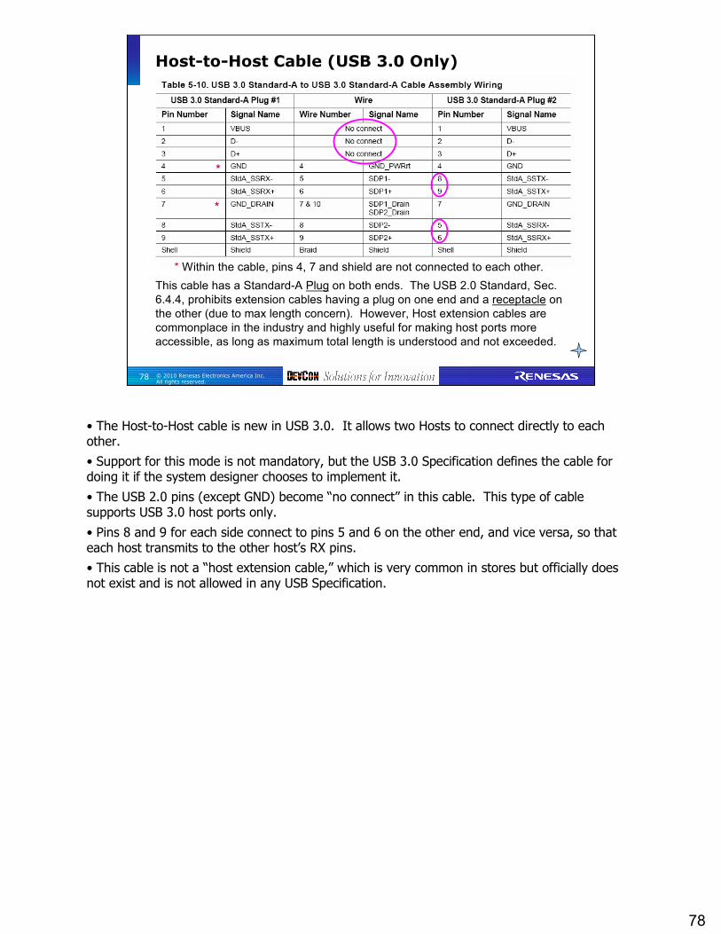
78
78 © 2010 Renesas Electronics America Inc. All rights reserved.
Host-to-Host Cable (USB 3.0 Only)
This cable has a Standard-A Plug on both ends. The USB 2.0 Standard, Sec.
6.4.4, prohibits extension cables having a plug on one end and a receptacle on
the other (due to max length concern). However, Host extension cables are
commonplace in the industry and highly useful for making host ports more
accessible, as long as maximum total length is understood and not exceeded.
*
*
* Within the cable, pins 4, 7 and shield are not connected to each other.
• The Host-to-Host cable is new in USB 3.0. It allows two Hosts to connect directly to each other.
• Support for this mode is not mandatory, but the USB 3.0 Specification defines the cable for doing it if the system designer chooses to implement it.
• The USB 2.0 pins (except GND) become “no connect” in this cable. This type of cable supports USB 3.0 host ports only.
• Pins 8 and 9 for each side connect to pins 5 and 6 on the other end, and vice versa, so that each host transmits to the other host’s RX pins.
• This cable is not a “host extension cable,” which is very common in stores but officially does not exist and is not allowed in any USB Specification.

79
79 © 2010 Renesas Electronics America Inc. All rights reserved.
USB 3.0 Cable Length
Max cable length for USB 3.0 depends on cable quality and max budgets for signal losses and DC voltage drops.
Probably about 3 meters max for well constructed USB 3.0 cables.
For further details, refer to the USB 3.0 Standard, Sec. 5.5.7, 5.6.1.1.3, 5.6.1.3.1, 11.4.2 and 11.4.7.
External hubs can be used to achieve greater total distances from host to device, with each link limited to about 3 meters.
Solutions involving fiber optic links require further care to satisfy turnaround timing requirements as well as signal attenuation and DC voltage requirements. Fiber optic links are beyond the scope of the USB standards.
• 3m is usually a fairly good estimate of useful USB 3.0 cable length for reasonably well constructed USB 3.0 cables, but the official specification is stated in terms of loss budgets rather than a specific cable length.

80
80 © 2010 Renesas Electronics America Inc. All rights reserved.
USB 3.0 Supports USB 2.0
In order for a device to run in USB 3.0 SS mode, the entire path from host to
device must be SS-capable, including the host port, intervening hub ports (if any),
and the device port, with USB 3.0 cables connecting all the USB links in the path
together. Otherwise, the device will run in a USB 2.0 mode.
• This table shows that USB 3.0 and USB 2.0 are almost completely interchangeable for functional operation, except for plugging a USB 3.0 “B” plug (standard or micro) into a USB 2.0 “B” receptacle.
• The USB 3.0 Specification also defines a “powered-B” connector for cases such as a wireless USB hub (dongle) plugging into a self-powered peripheral such as a printer. The Powered-B case is not discussed further in this presentation. Refer to Sections 11.4.6 and 5.3.3 in the USB 3.0 Specification for details.

81
81 © 2010 Renesas Electronics America Inc. All rights reserved.
5 Gbps Signals Need very Careful PCB Layout
Signals in each SS pair must be routed as a controlled impedance differential pair; tight symmetry; safe distance from other metal of any kind.
Need continuous GND layer adjacent to any layer that carries 5 Gbps signals; GND layer on both sides of any embedded 5 Gbps layer. PCB will need at least 4 layers minimum.
Series capacitors must be close together, symmetrically placed.
Signals in each 5 Gbps pair must be length matched to within 5 mils. Use “serpentine” routing if needed to get 5 mil length match within each 5 Gbps pair. (No need to match lengths of one pair to another pair.)
• This slide summarizes the most important layout guidelines for the USB 3.0 SS signals.
• Refer to the Renesas Board Layout Guide for complete details of our layout recommendations.
• These recommendations also apply to the 5 Gbps PCI Express differential pairs and REFCLK.

82
82 © 2010 Renesas Electronics America Inc. All rights reserved.
Additional Notes:
Each 5 Gbps pair should route entirely on the same PCB layer if possible.
If switching to another layer is unavoidable, place GND vias symmetrically close to the signal vias. Also maintain large clearance around signal vias (away from any nearby metal on any layer).
Maintain large metal clearance around connector pins as well as vias for any 5 Gbps signal.
Do not exceed 4 inches maximum total trace length from USB 3.0 SS transmitter or receiver to the USB 3.0 connector.
At turning points, traces should bend at 45 degree angle or smooth circle, never a 90-degree corner.
Avoid any transmission line stubs on 5 Gbps signals.
These guidelines apply to PCIe as well as USB 3.0.
Follow VLSI vendor’s PCB Layout Guide fully!
5 Gbps Signals Need very Careful PCB Layout
• This slide summarizes additional important layout guidelines for the USB 3.0 SS signals.
• Refer to the Renesas Board Layout Guide for complete details of our layout recommendations.
• These recommendations also apply to the 5 Gbps PCI Express differential pairs and REFCLK, except that additional distance is allowed for PCIe signals from the µPD720200 to the PCI Express card-edge connector, since PCIe signals don’t support external cables.
• Similar, but less stringent guidelines also apply to the USB 2.0 HS differential pairs. Refer to Renesas layout documents and evaluation card designs for further details.

83
83 © 2010 Renesas Electronics America Inc. All rights reserved.
Unique K-codes for Symbol Lock
3 symbols have 5 consecutive 1’s or 5 consecutive 0’s: K28.1, K28.5, K28.7. All other K and D symbols have 4 max.
A few back-to-back pairs of symbols can produce 5 consecutive 1’s or 5 consecutive 0’s where they join, but they don’t produce K28.5.
• One of the key properties of K28.5 (COM) is that it has 5 consecutive one’s. The RD+ version has 5 consecutive zeroes. Extremely few 10-bit symbols have that property. Two others, K28.1 and K28.7, are highlighted in this slide.
• Even back-to-back combinations of symbols usually do not result in 5 consecutive one’s or 5 consecutive zeroes. And they never produce K28.5.

84
84 © 2010 Renesas Electronics America Inc. All rights reserved.
LFPS Events
Event type signified primarily by burst duration (tBurst)
Some event types also use burst repetition (tRepeat)
U1, U2 and U3 refer to link power states
Ping.LFPS = 40 ns to 200 ns
Polling.LFPS = 0.6 us to 1.4 us
U1 Exit = 300 ns to 900 ns (or 2 ms)
U2 / Loopback Exit = 80 us to 2 ms
U3 Wakeup = 80 us to 10 ms
tReset = 80 ms to 120 ms
• Here is additional detail on the types of LFPS events and the burst durations for each.

85
85 © 2010 Renesas Electronics America Inc. All rights reserved.
Transaction
Packets (TP)

86
86 © 2010 Renesas Electronics America Inc. All rights reserved.
Types of Transaction Packets (TP)
• The Subtype field in a TP, Dword 1, bits 0-3, specifies the type of TP.
87
87 © 2010 Renesas Electronics America Inc. All rights reserved.
Types of Transaction Packets (TP, cont.)
ACK: Acknowledgement
NRDY: Target temporarily not ready, need to wait
ERDY: Endpoint now ready after prior NRDY
STATUS: Completion of a Control Transfer
STALL: Hardware fault, unable to continue (or error detected during a Control Transfer)
DEV_NOTIFICATION: Notification of asynchronous status change within a device
PING: Alerts an isochronous target to wake up if it is sleeping
PING_RESPONSE: Target response to PING
• Here is a summary of what the various types of TP packets are used for.
• Usually an engineer designing and debugging a board-level product utilizing USB 3.0 technology won’t need to deal with all these TP types and their details unless a problem arises that requires attachment of a USB 3.0 protocol analyzer and interpretation of the packet-level traffic sequences recorded by the analyzer. And protocol analyzers typically decode the various fields in the packet and display that information in understandable text for the engineer to study further.
• If the engineer finds something in the analyzer capture that doesn’t quite make sense, the engineer can ask, “Why is the link doing that?” The engineer can then refer to the USB 3.0 Specification as needed for further details about what the various TP types and fields mean.

88
88 © 2010 Renesas Electronics America Inc. All rights reserved.
ACK Transaction Packet
• Here is a more detailed view of the ACK packet format (a type of Transaction Packet, TP).
• The Type field is set to ACK. The Route String specifies the required path through any external hubs to reach the endpoint device.
• The Device Address field serves the same purpose as in USB 2.0. It specifies the assigned USB address of the endpoint device.
• Various additional fields exist in an ACK, also. These are all discussed more fully in the USB 3.0 Specification.
• Note the Link Control Word at the end of the packet. Note also that the Dwords in this format are sent in order from 0 through 3, and the bytes in each Dword are transmitted in LSB-to-MSB order (right to left in the diagram). The Link Control Word is the last word transmitted, immediately following the CRC-16 field.
• There can be multiple “streams” for each Device Address. This feature will not be discussed further in this presentation and isn’t discussed in much detail in the USB 3.0 Specification, but it is extremely important for efficient file read/write to mass storage devices, and has significant hardware implications in devices and Root Hubs.
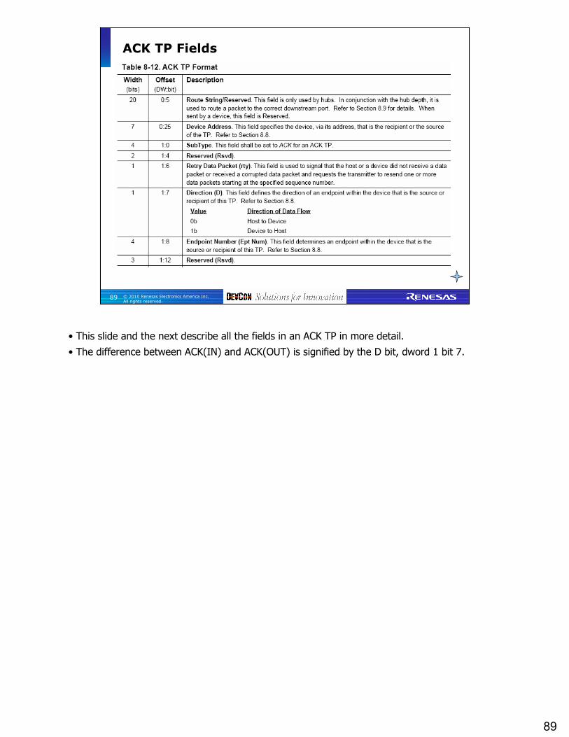
89
89 © 2010 Renesas Electronics America Inc. All rights reserved.
ACK TP Fields
• This slide and the next describe all the fields in an ACK TP in more detail.
• The difference between ACK(IN) and ACK(OUT) is signified by the D bit, dword 1 bit 7.

90
90 © 2010 Renesas Electronics America Inc. All rights reserved.
ACK TP Fields (2)
• Continuation of the field descriptions for ACK packets.
• All Transaction Packets (TP) have the same basic format, with various differences as needed for the particular TP type.

91
91 © 2010 Renesas Electronics America Inc. All rights reserved.
Not Ready (NRDY) Transaction Packet
• NRDY is sent by a device instead of ACK when the device is not immediately ready to send ACK.
• The link partner should stop further attempts to complete the transaction until the target is ready.
• The target should send ERDY to notify its link partner that it is now ready.

92
92 © 2010 Renesas Electronics America Inc. All rights reserved.
Endpoint Ready (ERDY) Transaction Packet
• See NRDY description for the typical usage of this TP type as well as the NRDY type.
• Note that ERDY contains the NumP field used to define the allowable size of data packet bursts. Bursting is discussed further on an earlier slide.
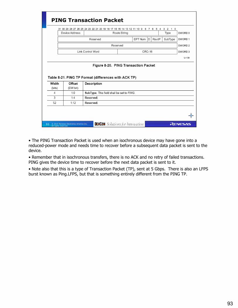
93
93 © 2010 Renesas Electronics America Inc. All rights reserved.
PING Transaction Packet
• The PING Transaction Packet is used when an isochronous device may have gone into a reduced-power mode and needs time to recover before a subsequent data packet is sent to the device.
• Remember that in isochronous transfers, there is no ACK and no retry of failed transactions. PING gives the device time to recover before the next data packet is sent to it.
• Note also that this is a type of Transaction Packet (TP), sent at 5 Gbps. There is also an LFPS burst known as Ping.LFPS, but that is something entirely different from the PING TP.

94
94 © 2010 Renesas Electronics America Inc. All rights reserved.
PING_RESPONSE Transaction Packet
• When an isochronous device in reduced power mode is fully recovered and ready to handle the next isochronous data transaction, the device sends PING_RESPONSE in response to a PING TP.

95
95 © 2010 Renesas Electronics America Inc. All rights reserved.
STATUS Transaction Packet
Terminates a Control Transfer
• Each Control Transfer is terminated by a STATUS TP, shown in this slide.
• The format of STATUS is almost identical to ACK, except for the Sub Type code.
• Remember, also, that all TP formats are forms of Header Packets and contain a Link Control Word at the end, like all other Header Packets.

96
96 © 2010 Renesas Electronics America Inc. All rights reserved.
More on Header Packets

97
97 © 2010 Renesas Electronics America Inc. All rights reserved.
Link Control Word in all Header Packets
• All Header Packets end with a Link Control Word (LCW, 2 bytes), having the format shown in the diagram.
• The fields in the LCW are described further on the next slide.
• For added error detection, the LCW includes a 5-bit CRC checksum.
• The USB 3.0 Specification defines exactly what the link is supposed to do when an error of any kind is detected. Development engineers rarely need to be concerned with all the details of error detection and recovery until a specific problem arises and needs to be debugged. At that point, a protocol analyzer will record exactly what is going on, and the USB 3.0 Specification can be consulted to understand what it means.
• Protocol analyzers may also provide excerpts or summaries of USB 3.0 Specification information in the in-build “help” files on the analyzer itself.

98
98 © 2010 Renesas Electronics America Inc. All rights reserved.
Link Control Word in all Header Packets
• This table lists the individual bit fields in a Link Control Word (LCW).
• The USB 3.0 Specification describes the Link Control Word as assisting with link level flow control, but the specification doesn’t elaborate very much on exactly how the LCW does that. Numerous brief references to the LCW can be found by performing a string search on “Link Control Word” in the USB 3.0 Specification. The best references appear to be in Section 3.2.4.1, 7.2.1.1.3, and 8.3.1.4.

99
99 © 2010 Renesas Electronics America Inc. All rights reserved.
Data Packet (DPH + DPP)
• Here is an expanded view of the various fields in a data packet, especially the Data Packet Header (DPH).
• As we saw in an earlier slide, the DPP contains nothing but K-code framing and D-code data (and CRC), so there are no additional information fields in the DPP other than the payload data itself.

100
100 © 2010 Renesas Electronics America Inc. All rights reserved.
Data Packet Header Fields
Ept Num
S
EOB
Data Length
• This table lists the fields in a DPH.
• The “S” bit in dword 1, bit 15, is discussed further in connection with Control Transfers. S=1 signifies that the packet is for a Setup Transaction instead of a data packet. For normal data transfer, S=0.
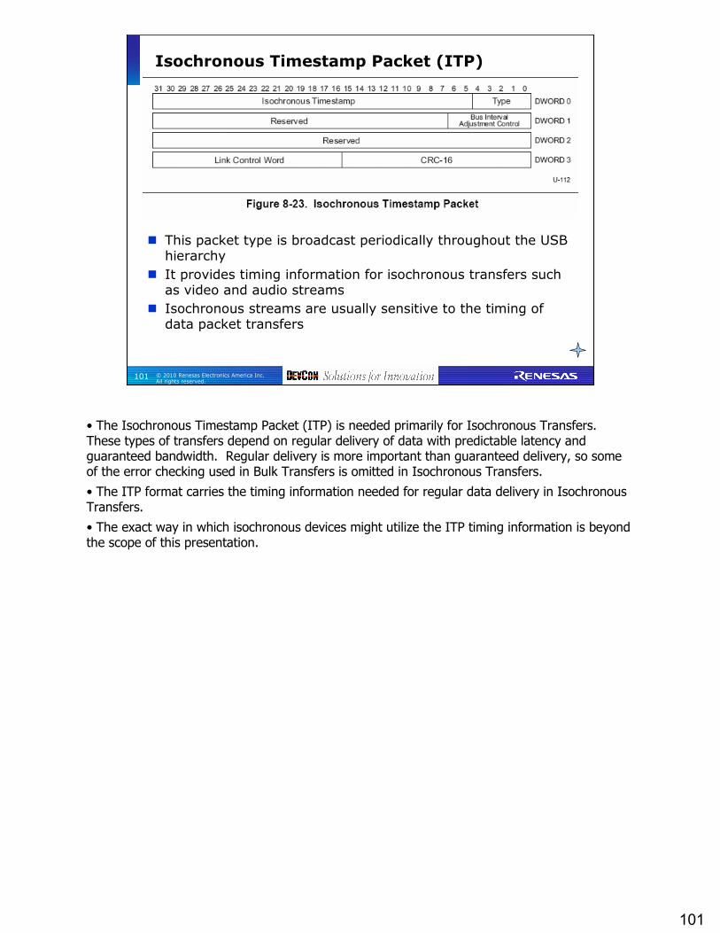
101
101 © 2010 Renesas Electronics America Inc. All rights reserved.
Isochronous Timestamp Packet (ITP)
This packet type is broadcast periodically throughout the USB hierarchy
It provides timing information for isochronous transfers such as video and audio streams
Isochronous streams are usually sensitive to the timing of data packet transfers
• The Isochronous Timestamp Packet (ITP) is needed primarily for Isochronous Transfers. These types of transfers depend on regular delivery of data with predictable latency and guaranteed bandwidth. Regular delivery is more important than guaranteed delivery, so some of the error checking used in Bulk Transfers is omitted in Isochronous Transfers.
• The ITP format carries the timing information needed for regular data delivery in Isochronous Transfers.
• The exact way in which isochronous devices might utilize the ITP timing information is beyond the scope of this presentation.

102
102 © 2010 Renesas Electronics America Inc. All rights reserved.
Isochronous Timestamp Packet Fields
• The main content of an ITP is the Isochronous Timestamp value (ITS). There is very little additional content.
• Since the ITP is broadcast to all devices, no Route String is needed in an ITP.

103
103 © 2010 Renesas Electronics America Inc. All rights reserved.
Link Management Packet (LMP)
LMP is used for managing a single link
LMP is a type of Header Packet
LMP is different from the Link Control Word at the end of all Header Packets (including LMP, as shown above)
LMP is different from the Link Command Packet Type
• As its name implies, the Link Management Packet (LMP) is used for managing a single link.
• LMP’s are not forwarded beyond the immediate link partners on a single link.
• They take care of various miscellaneous issues relating to a single link.
• Note that an LMP is a type of Header Packet and contains a Link Control Word, like all other Header Packets. (Even ITP contains an LCW.)
• However, LMP should not be confused with a Link Command, which is an entirely different packet format discussed separately.
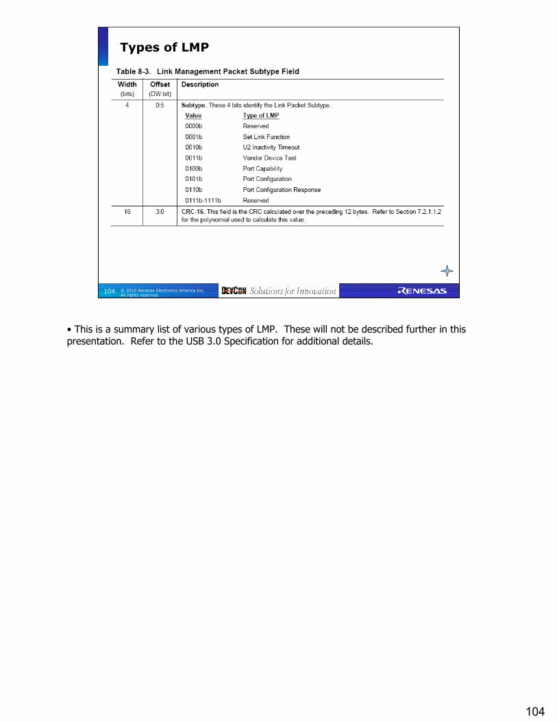
104
104 © 2010 Renesas Electronics America Inc. All rights reserved.
Types of LMP
• This is a summary list of various types of LMP. These will not be described further in this presentation. Refer to the USB 3.0 Specification for additional details.

105
105 © 2010 Renesas Electronics America Inc. All rights reserved.
Link Command Packets

106
106 © 2010 Renesas Electronics America Inc. All rights reserved.
Link Command Packet Type
K-Codes
Start Link
Command
This is not a Link Management Packet (LMP)
• The Link Command Packet format is always 8 symbols in length. The first 4 symbols are always K-codes.
• The remaining symbols consist of two Link Command Words, 2 symbols each. The 2 Link Command Words use D-codes.
• Note that this is a completely separate command format from the LMP Header Packet. This command is not a Header Packet.
• The protocol rules allow for one of the SLC symbols to be dropped but still leave the packet recognizable as a valid Link Command.

107
107 © 2010 Renesas Electronics America Inc. All rights reserved.
Link Command Word in a Link Command Packet
This is different from the Link Control Word used in Header Packets. The Link Command Word shown above is not part of a Header Packet.
• Here is some additional detail for the two Link Command Words.
• Note the 5-bit CRC checksum for 11 bits of Link Command Information.
• Also note that this format must not be confused with the Link Control Word that is used in Header Packets.

108
108 © 2010 Renesas Electronics America Inc. All rights reserved.
Link Command Usage
Ensuring successful packet transfer: LGOOD, LBAD, LRTY (retry).
Link flow control: LCRD (Link Credit, i.e., Rx buffer space available).
Link power management: LGO, LAU (accept), LXU (reject), LPMA (Link Power Management Ack).
LUP: Upstream port present in “U0” power state (sent every 10 usec during lack of other link packet activity).
• The 11 bits of Command Information in each Link Command Word allow the types of Link Commands listed in the slide to be defined.
• LBAD means the Link is Bad. LRTY means Link Retry.
• Other Link Commands are used for link flow control, link power management, and periodic upstream port present notifications to its link partner.

109
109 © 2010 Renesas Electronics America Inc. All rights reserved.
Link Training & Status
State Machine (LTSSM)

110
110 © 2010 Renesas Electronics America Inc. All rights reserved.
Major Port States
Rx.Detect Looking for link partner Typically entered after some type of reset completion Also entered upon link partner disconnect Partner is detected by its Rx termination impedance
Polling Performing "link training" (initializing the link for full SS operation) Typically entered from Rx.Detect after a link partner is detected
U0 Link fully operational (packets, separated by logical idle intervals) Typically entered from Polling or Recovery
U1, U2, U3
Link inactive, reduced power (electrical idle) Exits to Recovery
Recovery Link needs retraining and is able to do it
Typically entered when link needs to return to U0
• Upon completion of a link reset, the ports connected to the link go into Receiver Detect mode, looking for a link partner.
• A partner is found if it is presenting a proper line termination impedance to the transmitter on the other end of the link, and is responding with the expected kinds of Training Sequence patterns on its own transmit differential pair.
• Detection of a line termination advances the port to the Polling state, where it checks the responses, if any, coming back from the other end of the link.
• If the expected responses come back when they should, the port goes into the fully powered and operational mode, known as U0.
• After various periods of link idle time, the link may go into reduced power modes known as U1, U2 and eventually U3. These are successively deeper power reduction modes, with correspondingly longer latencies to recover back to U0 when the link needs to perform new activity.
• When returning to full operation, a port in U1, U2 or U3 state generally goes through the Recovery state to allow link retraining and return to U0.

111
111 © 2010 Renesas Electronics America Inc. All rights reserved.
Major Port States (2)
SS.Disabled
SS inoperative; port may operate as USB 2.0 Typically entered by software command or VBUS down
Hot Reset Downstream port requesting upstream port to reset
Typically entered from Polling or Recovery
Compliance Mode For transmitter compliance testing Typically entered from Polling if no link partner is present
Loopback For bit-error rate testing (BERT) Typically entered from Polling or Recovery by software request
SS.Inactive Link inoperable, needing software intervention to recover Typically entered by abnormal protocol timeout or other major error condition Exits automatically to Rx.Detect if an Rx disconnect is detected
“LTSSM” refers to Link Training and Status State Machine
• The port goes into SS.Disabled state if no link partner is present. The link can then utilize the USB 2.0 signals in the cable to operate in a USB 2.0 mode in accord with standard USB 2.0 protocol.
• There is also provision in the link training sequences to put a link into a mode known as Hot Reset, or a diagnostic Loopback mode for error rate testing.
• Compliance Mode is entered if the other end of the link is passively terminated, i.e., a termination detected, but no active link partner is responding. Compliance mode is used for electrical eye pattern measurement and compliance testing.
• Serious error conditions can result in a port going into SS.Inactive mode, in which the link stops operating until software intervenes.
• The USB 3.0 Specification defines detailed Link Training and Status State Machines (LTSSM) for all these link states and sub-states.

112
112 © 2010 Renesas Electronics America Inc. All rights reserved.
Link Training Overview (Polling State)
Polling.LFPS substate Polling.LFPS bursts are sent back an forth in LFPS mode. Establishes basic DC operating conditions on the link, and successful
handshaking between the link partners. Exits to Compliance Mode after 360 ms if there is no active link partner.
Polling.RxEQ substate Link partners send 65536 TSEQ sequences for receiver equalization training
Polling.Active substate Link partners transmit TS1 sequences. Upon receiving TS1 response, each partner begins transmitting TS2.
Polling.Configuration substate Link partners transmit TS2 sequences. Upon receiving TS2 response, each partner exits to Polling.Idle
Polling.Idle substate
Link partners transmit Logical Idle. Exit to U0 for normal operation May exit to Loopback, SS.Disabled, Hot Reset, or Rx.Detect if directed or
timeout
• This is a more detailed look at the Polling state mentioned earlier. Most of the essential link training activity occurs during this state.
• The process of checking for the presence of a link partner actually involves sending and receiving a series of LFPS bursts to establish the DC conditions on the link as well as the presence of an active link partner.
• Next comes the TSEQ phase, for receiver equalization training.
• TSEQ is followed by the TS1 and TS2 handshake intervals, followed finally by the Polling.Idle state in which the link is fully operational in U0 power mode, but idle, i.e., continuous Logical Idle symbols (D0.0).
• Various possible exit paths are defined in USB 3.0 from Polling.Idle to other states such as Loopback, SS.Disabled, Hot Reset, or directed return to Rx.Detect.
• The link can remain in Polling.Idle (Logical Idle) indefinitely, until software directs otherwise or initiates packet traffic.

113
Renesas Electronics America Inc.