ics for communications - digi-key sheets/infineon pdfs/peb 20320.pdf– on-chip 64-channel dma...
TRANSCRIPT

ICs for Communications
Multichannel Network Interface Controller for HDLCMUNICH32
PEB 20320 Version 3.4
User’s Manual 01.2000DS3
•
For questions on technology, delivery and prices please contact the Infineon Technologies Offices in Germany or the Infineon Technologies Companies and Representatives worldwide: see our webpage at http://www.infineon.com
•
PEB 20320 Revision History: Current Version: 01.2000
Previous Version: User’s Manual 1998-06-01 DS2 (V3.4)
Page(in previous Version)
Page(in current Version)
Subjects (major changes since last revision)
Package P-TQFP-176-1 removed from User’s Manual.
Edition 01.2000Published by Infineon Technologies AG,SC,Balanstraße 73,81541 München© Infineon Technologies AG 2000.All Rights Reserved.Attention please!As far as patents or other rights of third parties are concerned, liability is only assumed for components, not for applications, processes and circuits implemented within components or assemblies.The information describes the type of component and shall not be considered as assured characteristics.Terms of delivery and rights to change design reserved.Due to technical requirements components may contain dangerous substances. For information on the types in question please contact your nearest Infineon Technologies Office.Infineon Technologies AG is an approved CECC manufacturer.PackingPlease use the recycling operators known to you. We can also help you – get in touch with your nearest sales office. By agreement we will take packing material back, if it is sorted. You must bear the costs of transport. For packing material that is returned to us unsorted or which we are not obliged to accept, we shall have to invoice you for any costs incurred.Components used in life-support devices or systems must be expressly authorized for such purpose!Critical components1 of the Infineon Technologies AG, may only be used in life-support devices or systems2 with the express written approval of the Infineon Technologies AG.1 A critical component is a component used in a life-support device or system whose failure can reasonably be
expected to cause the failure of that life-support device or system, or to affect its safety or effectiveness of that device or system.
2 Life support devices or systems are intended (a) to be implanted in the human body, or (b) to support and/or maintain and sustain human life. If they fail, it is reasonable to assume that the health of the user may be en-dangered.
ABM®, AOP®, ARCOFI®, ARCOFI®-BA, ARCOFI®-SP, DigiTape®, EPIC®-1, EPIC®-S, ELIC®, FALC®54, FALC®56, FALC®-E1, FALC®-LH, IDEC®, IOM®, IOM®-1, IOM®-2, IPAT®-2, ISAC®-P, ISAC®-S, ISAC®-S TE, ISAC®-P TE, ITAC®, IWE®, MUSAC®-A, OCTAT®-P, QUAT®-S, SICAT®, SICOFI®, SICOFI®-2, SICOFI®-4, SICOFI®-4µC, SLICOFI® are registered trademarks of Infineon Technologies AG.
ACE™, ASM™, ASP™, POTSWIRE™, QuadFALC™, SCOUT™ are trademarks of Infineon Technologies AG.
PEB 20320
PrefaceThe Multichannel Network Interface Controller for HDLC (MUNICH32) is a MultichannelProtocol Controller for a wide area of telecommunication and data communicationapplications.
Organization of this Document
This User’s Manual is divided into 9 chapters. It is organized as follows:
• Chapter 1, IntroductionGives a general description of the product and its family, lists the key features, andpresents some typical applications.
• Chapter 2, Functional DescriptionThis chapter provides a detailed description of the interfaces and the protocol modes.
• Chapter 3, Operational DescriptionProvides a description of MUNICH32 reset procedure and initialization.
• Chapter 4, Detailed Register DescriptionGives a detailed description of the shared memory organization.
• Chapter 5, Application Notes
• Chapter 6, Application Hints
• Chapter 7, Electrical CharacteristicsGives a detailed description of all electrical DC and AC characteristics and providestiming diagrams and values for all interfaces.
• Chapter 8, Package Outlines
• Chapter 9, AppendixThis chapter provides source code examples.
Your Comments
We welcome your comments on this document as we are continuously aiming atimproving our documentation. Please send your remarks and suggestions by e-mail to
Please provide in the subject of your e-mail:device name (MUNICH32), device number (PEB 20320), device version (Version 3.4),
and in the body of your e-mail:document type (User’s Manual), issue date (01.2000) and document revision number(DS3).
User’s Manual 3 01.2000

PEB 20320
User’s Manual 4 01.2000

PEB 20320
Table of Contents Page
1 Introduction . . . . . . . . . . . . . . . . . . . . . . . . . . . . . . . . . . . . . . . . . . . . . . . . .71.1 Features . . . . . . . . . . . . . . . . . . . . . . . . . . . . . . . . . . . . . . . . . . . . . . . .81.2 Pin Configuration . . . . . . . . . . . . . . . . . . . . . . . . . . . . . . . . . . . . . . . . . . . . .111.3 Pin Definitions and Functions . . . . . . . . . . . . . . . . . . . . . . . . . . . . . . . . . . .121.4 Logic Symbol . . . . . . . . . . . . . . . . . . . . . . . . . . . . . . . . . . . . . . . . . . . . . . . .221.5 Functional Block Diagram . . . . . . . . . . . . . . . . . . . . . . . . . . . . . . . . . . . . . .231.6 System Integration . . . . . . . . . . . . . . . . . . . . . . . . . . . . . . . . . . . . . . . . . . . .25
2 Functional Description . . . . . . . . . . . . . . . . . . . . . . . . . . . . . . . . . . . . . . .322.1 Serial Interface . . . . . . . . . . . . . . . . . . . . . . . . . . . . . . . . . . . . . . . . . . . . . . .322.2 Microprocessor Interface . . . . . . . . . . . . . . . . . . . . . . . . . . . . . . . . . . . . . . .382.2.1 Intel Mode . . . . . . . . . . . . . . . . . . . . . . . . . . . . . . . . . . . . . . . . . . . . . . . .392.2.2 Motorola Mode . . . . . . . . . . . . . . . . . . . . . . . . . . . . . . . . . . . . . . . . . . . . .432.2.3 DMA Priorities . . . . . . . . . . . . . . . . . . . . . . . . . . . . . . . . . . . . . . . . . . . . .462.3 Basic Functional Principles . . . . . . . . . . . . . . . . . . . . . . . . . . . . . . . . . . . . .472.4 Detailed Protocol Description . . . . . . . . . . . . . . . . . . . . . . . . . . . . . . . . . . .762.5 Boundary Scan Unit . . . . . . . . . . . . . . . . . . . . . . . . . . . . . . . . . . . . . . . . . .126
3 Operational Description . . . . . . . . . . . . . . . . . . . . . . . . . . . . . . . . . . . . .1313.1 Reset State . . . . . . . . . . . . . . . . . . . . . . . . . . . . . . . . . . . . . . . . . . . . . . . .1313.2 Initialization Procedure . . . . . . . . . . . . . . . . . . . . . . . . . . . . . . . . . . . . . . .132
4 Detailed Register Description . . . . . . . . . . . . . . . . . . . . . . . . . . . . . . . . .1344.1 Organization of the Shared Memory . . . . . . . . . . . . . . . . . . . . . . . . . . . . .1344.2 Control and Configuration Section . . . . . . . . . . . . . . . . . . . . . . . . . . . . . . .1364.2.1 Action Specification (Read Once After Each Action Request Pulse) . . .1364.2.2 Interrupt Queue Specification . . . . . . . . . . . . . . . . . . . . . . .1404.2.3 Interrupt Information . . . . . . . . . . . . . . . . . . . . . . . . . . . . . . . . . . . . . . .1414.2.4 Time Slot Assignment . . . . . . . . . . . . . . . . . . . . . . . . . . . . . . . . . . . . . .1484.2.5 Channel Specification . . . . . . . . . . . . . . . . . . . . . . . . . . . . . . . . . . . . . .1494.2.6 Current Receive and Transmit Descriptor Address . . . . . . . . . . . . . .1614.3 Transmit Descriptor . . . . . . . . . . . . . . . . . . . . . . . . . . . . . . . . . .1624.4 Receive Descriptor . . . . . . . . . . . . . . . . . . . . . . . . . . . . . . . . . .168
5 Application Notes . . . . . . . . . . . . . . . . . . . . . . . . . . . . . . . . . . . . . . . . . .1735.1 Test Loops . . . . . . . . . . . . . . . . . . . . . . . . . . . . . . . . . . . . . . . . . . . . . . . . .1735.1.1 Test Loop Definitions for the MUNICH32 . . . . . . . . . . . . . . . . . . . . . . .1735.1.1.1 Internal Complete Test Loop . . . . . . . . . . . . . . . . . . . . . . . . . . . . . . .1735.1.1.2 Internal Channelwise Test Loop . . . . . . . . . . . . . . . . . . . . . . . . . . . .1745.1.1.3 External Complete Test Loop . . . . . . . . . . . . . . . . . . . . . . . . . . . . . .1745.1.1.4 External Channelwise Test Loop . . . . . . . . . . . . . . . . . . . . . . . . . . . .1755.1.2 Test Loop Activation . . . . . . . . . . . . . . . . . . . . . . . . . . . . . . . . . . . . . . .1765.1.3 Test Loop Deactivation and Switching . . . . . . . . . . . . . . . . . . . . . . . . . .1765.1.3.1 Software Operations . . . . . . . . . . . . . . . . . . . . . . . . . . . . . . . . . . . . .177
User’s Manual 5 01.2000

PEB 20320
Table of Contents Page
5.1.3.2 Hardware Reset Operations . . . . . . . . . . . . . . . . . . . . . . . . . . . . . . .1775.1.4 Test Loop Examples . . . . . . . . . . . . . . . . . . . . . . . . . . . . . . . . . . . . . . .1785.1.4.1 Internal Channelwise Test Loop . . . . . . . . . . . . . . . . . . . . . . . . . . . .1785.1.4.2 External Channelwise Test Loop . . . . . . . . . . . . . . . . . . . . . . . . . . . .1805.2 MUNICH32 in a LAN/WAN Router . . . . . . . . . . . . . . . . . . . . . . . . . . . . . .1825.2.1 Introduction . . . . . . . . . . . . . . . . . . . . . . . . . . . . . . . . . . . . . . . . . . . . . .1825.2.2 Hardware . . . . . . . . . . . . . . . . . . . . . . . . . . . . . . . . . . . . . . . . . . . . . . . .1835.2.3 Software . . . . . . . . . . . . . . . . . . . . . . . . . . . . . . . . . . . . . . . . . . . . . . . . .1885.2.3.1 Device Driver Module MUNICH32 . . . . . . . . . . . . . . . . . . . . . . . . . . .1915.2.3.2 Application Module MROUTE . . . . . . . . . . . . . . . . . . . . . . . . . . . . . .1945.2.4 Performance Considerations . . . . . . . . . . . . . . . . . . . . . . . . . . . . . . . . .1975.2.5 Final Remarks . . . . . . . . . . . . . . . . . . . . . . . . . . . . . . . . . . . . . . . . . . . .2015.2.6 Adaption of the 68040 µP Signals . . . . . . . . . . . . . . . . . . . . . . . . . . . . .2035.2.7 Schematics . . . . . . . . . . . . . . . . . . . . . . . . . . . . . . . . . . . . . . . . . . . . . .2055.3 Memory Bus Occupancy for a Single MUNICH32 . . . . . . . . . . . . . . . . . . .2145.3.1 Bus Occupancy Calculations . . . . . . . . . . . . . . . . . . . . . . . . . . . . . . . . .2175.3.2 Bus Occupancy for Idle Tx Channels . . . . . . . . . . . . . . . . . . . . . . . . . .218
6 Application Hints . . . . . . . . . . . . . . . . . . . . . . . . . . . . . . . . . . . . . . . . . . .2206.1 Frequency Adaption in an Intel 368 Common Bus System . . . . . . . . . . . .2206.2 MUNICH32 Memory Space Requirement . . . . . . . . . . . . . . . . . . . . . . . . .2236.3 Serial Interface to different PCM Systems . . . . . . . . . . . . . . . . . . . . . . . . .2246.3.1 MUNICH32 for SIEMENS Primary Access Interface . . . . . . . . . . . . . . .2246.3.2 MUNICH32 in Systems with MITEL ST BUS . . . . . . . . . . . . . . . . . . . . .227
7 Electrical Characteristics . . . . . . . . . . . . . . . . . . . . . . . . . . . . . . . . . . . .2297.1 Absolute Maximum Ratings . . . . . . . . . . . . . . . . . . . . . . . . . . . . . . .2297.2 DC Characteristics . . . . . . . . . . . . . . . . . . . . . . . . . . . . . . . . . . . . . . . . . . .2307.3 Capacitances . . . . . . . . . . . . . . . . . . . . . . . . . . . . . . . . . . . . . . . . . . . . . . .2317.4 AC Characteristics . . . . . . . . . . . . . . . . . . . . . . . . . . . . . . . . . . . . . . . . . . .2317.5 Microprocessor Interface Intel Bus Mode . . . . . . . . . . . . . . . . . . . . . . . . .2327.6 Microprocessor Interface Motorola Bus Mode . . . . . . . . . . . . . . . . . . . . . .235
8 Package Outlines . . . . . . . . . . . . . . . . . . . . . . . . . . . . . . . . . . . . . . . . . . .242
9 Appendix . . . . . . . . . . . . . . . . . . . . . . . . . . . . . . . . . . . . . . . . . . . . . . . . .2439.1 Source Code Extract MUNICH32 . . . . . . . . . . . . . . . . . . . . . . . . . . . . . . .2439.2 Source Code . . . . . . . . . . . . . . . . . . . . . . . . . . . . . . . . . . . . . . . . . . . . . . .245
User’s Manual 6 01.2000

PEB 20320
Introduction
1 Introduction
The Multichannel Network Interface Controller for HDLC (MUNICH32) is a MultichannelProtocol Controller, which handles up to 32 data channels of a full duplex PCM highway.It performs layer 2 HDLC formatting/deformatting or V.110 and X.30 protocols up toa network data rate of 38.4 Kbit/s as well as transparent transmission for theDMI mode 0, 1 and 2. The processed data is passed on to an external memory sharedwith one or more host processors.
MUNICH32 is compatible with the LAPD ISDN (Integrated Services Digital Network)protocol specified by CCITT as well as with HDLC, SDLC, LAPB DMI protocols. Itprovides any rate adaption for time slot transmission data rate from 64 Kbit/s down to8 Kbit/s and the concatenation of any time slots to data channels, supporting the ISDNH0, H11, H12 superchannels.
Due to these functions the MUNICH32 can be used in a wide area of telecommunicationand data communication applications, e.g. in central office switches, for the connectionof a digital PABX to a host computer, as a central D-channel controller to 32 ISDN basicaccess D-channels or as a multiplexer for terminals and other peripherals. Up to4 MUNICH32s can be connected to one PCM highway, so a D-channel controller with128 channels can be achieved.
User’s Manual 7 01.2000

P-MQFP-160-1
Multichannel Network Interface Controller for HDLCMUNICH32
PEB 20320
Version 3.4 CMOS
1.1 Features
• Serial Interface– Up to 32 independent communication channels.– Serial multiplexed (full duplex) input/output for
2048-, 4096-, 1544- or 1536-Kbit/s PCM highways.
• Dynamic Programmable Channel Allocation– Compatible with T1/DS1 24-channel and CEPT
32-channel PCM byte format.
– Concatenation of any, not necessarily consecutive,
time slots to superchannels independently for receive and transmit direction.
– Support of H0, H11, H12 ISDN-channels.– Subchanneling on each time slot possible.
• Bit Processor Functions (adjustable for each channel)– HDLC Protocol
– Automatic flag detection and transmission– Shared opening and closing flag– Detection of interframe-time-fill change, generation of
interframe-time-fill ‘1’s or flags– Zero bit insertion – Flag stuffing and flag adjustment for rate adaption– CRC generation and checking (16 or 32 bits)– Transparent CRC option per channel and/or per message– Error detection (abort, long frame, CRC error, 2 categories
of short frames, non-octet frame content)– Special short frame mode to allow reception of ‘frames’ with a least on byte
length– ABORT/IDLE generation
User’s Manual 8 01.2000
Type Package
PEB 20320 P-MQFP-160-1

PEB 20320
Introduction
– V.110/X.30 Protocol– Automatic synchronization in receive direction, automatic generation of
the synchronization pattern in transmit direction– E / S / X bits freely programmable in transmit direction, van be changed
during transmission; changes monitored and reported in receive direction– Generation/detection of loss of synchronism– Bit framing with network data rates from 600 bit/s up to 38.4 Kbit/s
– Transparent Mode A– Slot synchronous transparent transmission/reception without frame structure– Bit-overwrite with fill/mask bits– Flag generation, flag stuffing, flag extraction, flag generation
in the abort case with programmable flag– Transparent Mode B
– Transparent transmission/reception in frames delimited by 00H flags– Shared opening and closing flag– Flag stuffing, flag detection, flag generation in the abort case– Error detection (non octet frame content, short frame, long frame)
– Transparent Mode R– Transparent transmission/reception with GSM 08.60 frame structure– Automatic 0000H flag generation/detection– Support of 40, 391/2, 401/2 octet frames– Error detection (non octet frame content, short frame, long frame)
– Protocol Independent– Channel inversion (data, flags, IDLE code)– Format conventions as in CCITT Q.921 § 2.8– Data over- and underflow detected
• Processor Interface– ON-CHIP 64-channel DMA controller with buffer chaining capability.– Compatible with Motorola 68020 processor family and
Intel 32-bit processor (80386).– 32 bit data bus and 32 bit address bus (4 Gbyte RAM addressable, Motorola and
Intel non-parity) or 28 bit address bus (256 Mbyte RAM addressable, Intel parity)– Intel parity mode with data byte parity (4 parity bits)
– Parity check for read accesses– Parity generation for write accesses
– Interrupt-circular buffer with variable size– Maskable interrupts for each channel– µP interface buffer of depth 16 long words for adaptive bus occupation
User’s Manual 9 01.2000

PEB 20320
Introduction
• General– Connection of up to four MUNICH32 supporting a
128-channel basic access D-channel controller.– ON-CHIP receive and transmit data buffer; the buffer size is 256 bytes each.– HDLC protocol or transparent mode, support of ECMA 102, CCITT I4.63 RA2,
V.110, X.30, DMI mode 0, 1, 2 (bit rate adaption), GSM 08.60 TRAU frames.– LOOP mode, complete loop as well as single channel loop– JTAG boundary scan test– Advanced low-power CMOS technology– TTL-compatible inputs/outputs– 160 pin P-MQFP package
User’s Manual 10 01.2000

PEB 20320
Introduction
1.2 Pin Configuration(top view)
Figure 1
ITP03487
Marking
A19
A9
D8
D18A18
D17
A12
A11
D10A10
D9
A8
INT/
INT
D31
A28/
DP0
D28
D27
A27
VSS
RSPRDATACI0
I/M
READY/DSACK
HLDA/BG
BGAC
K/PM
HOLD
/BR
DS/P
CHK
W,R
/R;W
D30
A30/
DP2
A26
D26
D25
D21
A21
D20
A20
Index
D19
D16
D15
A22
VSS D2
9
D3D4SSVD7 D0D1BE
0D2A3A4D5A5D6 BE
1
A7
A17
A15
A14D14
A13D13
D11
BE2
B16
BERR
AR
TSPTCLKN.C.
HLDAO/BGO
TEST
SCLKRESET
JTEST3JTEST2
JTEST0JTEST1
N.C.
RCLK
CI1
CI3CI4N.C.
MUNICH32PEB 20320
VSS
VDD D2
2 SSV
SSV V
DDD2
3A2
3D2
4A2
4V
SSV
DD A25
VSS
VDD
VSS
VDD
A29/
DP1
VSS
VDD
A31/
DP3
A16
D12
VDD
VSS
VDD A6 VDD
VSS
VSS
VDD
V VSS SS A2 VDD
VSS V D
DV
SS BE3
VDD
VSS
VSS AD
S/AS
VDD
VSS
N.C.N.C.
CI2
TDATA
N.C.N.C.
VSS
VDD
1160
150
140
130
121
10 20 30 4041
50
60
70
80100120 110 8190
VSS
VSS
VDD
VSSDDVDDV
DDV
VDDSSV
VV
SSDD
VVSS
DD
DDVSSV
SSVDD
VVSS
VVDD
SS
P-MQFP-160-1
User’s Manual 11 01.2000

PEB 20320
Introduction
1.3 Pin Definitions and Functions
Pin Definitions and Functions
Pin No.P-MQFP-160-1
Symbol Input (I)Output (O)
Function
83, 87, 88, 92, 97, 103, 104, 110, 111, 117, 123, 130, 136, 141, 144, 150, 151, 157, 3, 9, 10, 16, 22, 23, 29, 30, 36, 59, 62, 64, 77
VSS I Ground (0 V)All pins must have the same level.
73 I/M I Intel Bus Mode or Motorola Bus ModeBy connecting this pin to either VSS or VDD the bus interface can be adapted to either Intel or Motorola environment. The data is interpreted either in Intel or Motorola manner; i.e. little or big endian convention.I/M = low: Intel bus modeI/M = high: Motorola bus mode
39 A31
DP3
O
I/O
Address Bit 31(Intel non-parity/Motorola) tristate when unused.Data Parity 3 (Intel parity mode), bidirectional tristate line containing/expecting parity bit of D(31:24).
35 A30
DP2
O
I/O
Address Bit 30 (Intel non-parity/Motorola) tristate when unused.Data Parity 2 (Intel parity mode), bidirectional tristate line containing/expecting parity bit of D(23:16).
Note: Input pins that are unused in a specific configuration must be strapped to VSS.I/O or output pins that are unused in a specific configuration must be left open!
User’s Manual 12 01.2000

PEB 20320
Introduction
33 A29
DP1
O
I/O
Address Bit 29 (Intel non-parity/Motorola) tristate when unused.
Data Parity 1 (Intel parity mode), bidirectional tristate line containing/expecting parity bit of D(15:8)
28 A28
DP0
O
I/O
Address Bit 28 (Intel non-parity/Motorola) tristate when unused
Data Parity 0 (Intel parity mode), bidirectional tristate line containing/expecting parity bit of D(7:0)
26, 21, 19, 15, 13, 8, 6, 2, 160, 156, 154, 149, 147, 143, 139, 135, 133, 128, 126, 122, 120, 116, 114, 109, 107, 102
A(27:2) O Address Bustristate when unused.
91, 94, 96, 100 BE(3:0) O Byte Enable (Intel bus mode)The MUNICH32 provides word and long word transfer. The byte enables determine the address offset to the address A31 … A2, the actual word has been stored to.Address Offset Size (Motorola mode)Indicates the number of bytes remaining to be transferred for this access. These signals define the active sections of the data bus.In both cases these signals are tristate when unused.See Chapter 2.2 for details.
Pin Definitions and Functions (cont’d)
Pin No.P-MQFP-160-1
Symbol Input (I)Output (O)
Function
User’s Manual 13 01.2000
PEB 20320
Introduction
38, 34, 32, 27, 25, 20, 18, 14, 12, 7, 5, 1, 159, 153, 148, 146, 142, 138, 134, 132, 127, 125, 121, 119, 115, 113, 108, 106, 101, 99, 95
D(31:0) I/O Data BusThe data bus lines are bidirectional tristate lines which interface with the system’s data bus.
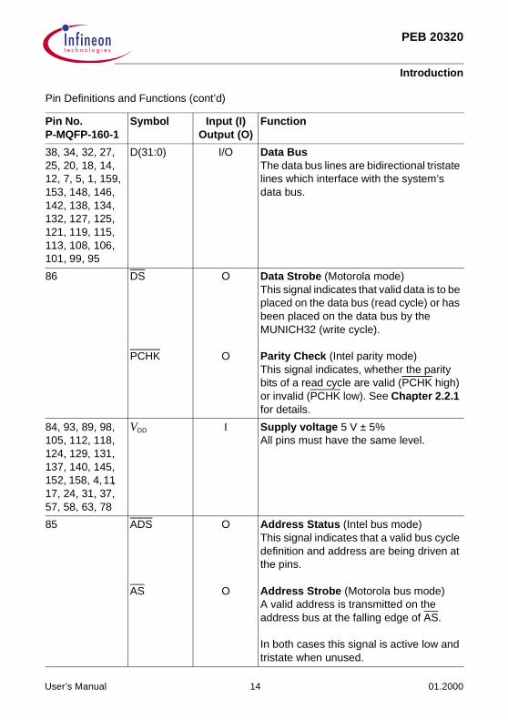
86 DS
PCHK
O
O
Data Strobe (Motorola mode)This signal indicates that valid data is to be placed on the data bus (read cycle) or has been placed on the data bus by the MUNICH32 (write cycle).
Parity Check (Intel parity mode)This signal indicates, whether the parity bits of a read cycle are valid (PCHK high) or invalid (PCHK low). See Chapter 2.2.1 for details.
84, 93, 89, 98, 105, 112, 118, 124, 129, 131, 137, 140, 145, 152, 158, 4,11, 17, 24, 31, 37, 57, 58, 63, 78
VDD I Supply voltage 5 V ± 5%All pins must have the same level.
85 ADS
AS
O
O
Address Status (Intel bus mode)This signal indicates that a valid bus cycle definition and address are being driven at the pins.
Address Strobe (Motorola bus mode)A valid address is transmitted on the address bus at the falling edge of AS.
In both cases this signal is active low and tristate when unused.
Pin Definitions and Functions (cont’d)
Pin No.P-MQFP-160-1
Symbol Input (I)Output (O)
Function
User’s Manual 14 01.2000
PEB 20320
Introduction
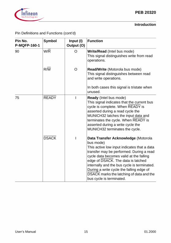
90 W/R
R/W
O
O
Write/Read (Intel bus mode)This signal distinguishes write from read operations.
Read/Write (Motorola bus mode)This signal distinguishes between read and write operations.
In both cases this signal is tristate when unused.
75 READY
DSACK
I
I
Ready (Intel bus mode)This signal indicates that the current bus cycle is complete. When READY is asserted during a read cycle the MUNICH32 latches the input data and terminates the cycle. When READY is asserted during a write cycle the MUNICH32 terminates the cycle.
Data Transfer Acknowledge (Motorola bus mode)This active low input indicates that a data transfer may be performed. During a read cycle data becomes valid at the falling edge of DSACK. The data is latched internally and the bus cycle is terminated. During a write cycle the falling edge of DSACK marks the latching of data and the bus cycle is terminated.
Pin Definitions and Functions (cont’d)
Pin No.P-MQFP-160-1
Symbol Input (I)Output (O)
Function
User’s Manual 15 01.2000

PEB 20320
Introduction
76 BERR I Bus Error (Intel and Motorola bus mode)This active low signal informs the MUNICH32 that a bus cycle error has occurred. The MUNICH32 terminates the bus cycle.In case of an erroneous read cycle in the control and configuration section an ‘Action Request Fail’ interrupt is generated and the action is suspended. In case of an erroneous read cycle in the transmit data section the corresponding frame is aborted and a FO interrupt is generated. In all other cases of read or write cycles terminated with an error condition no further actions are performed by the MUNICH32. Please see Chapter 2.2, ‘Microprocessor Interface’, first paragraph and Figure 18.As bus cycles are executed without time limit this signal prevents a hang-up situation of the MUNICH32.
74 B16 I Word Operation Setting this bit to VDD causes the MUNICH32 to perform 32-bit long word accesses to the shared memory, setting it to VSS causes the MUNICH32 to perform 16-bit word accesses on the data lines D(15:0) only. In 16-bit word access mode the data lines D(31:16) should be left open.This bit is not dynamic and should be set to VDD in Intel parity mode.
Pin Definitions and Functions (cont’d)
Pin No.P-MQFP-160-1
Symbol Input (I)Output (O)
Function
User’s Manual 16 01.2000

PEB 20320
Introduction
82 HOLD
BR
O
I/O
Bus Hold Request (Intel bus mode)This signal is driven high when the MUNICH32 requests the control of the bus.
Bus Request (Motorola bus mode)This signal is driven low when the MUNICH32 requests the control of the bus and is interpreted when another MUNICH32 wants to be the bus master.
79 HLDA
BG
I
I
Bus Hold Acknowledge (Intel bus mode)This active high signal indicates that the processor has released the control of the bus. The MUNICH32 starts the bus cycles.
Bus Grant (Motorola bus mode)This active low signal indicates that the MUNICH32 may assume the bus mastership.
81 BGACK
PM
I/O
I
Bus Grant Acknowledge (Motorola bus mode)This signal is driven low by the device, when it has become the bus master. It also informs the MUNICH32 whether another device is bus master.
Parity Mode (Intel bus mode)This signal has to be strapped to VDD before reset to enable the Intel parity mode or to VSS before reset to enable the Intel non-parity mode. It has to be left strapped during reset and operation.
Pin Definitions and Functions (cont’d)
Pin No.P-MQFP-160-1
Symbol Input (I)Output (O)
Function
User’s Manual 17 01.2000

PEB 20320
Introduction
80 HLDAO
BGO
O
O
Bus Hold Acknowledge Passing ON (Intel bus mode)If another MUNICH32 has initiated a HOLD REQUEST the HOLD ACKNOWLEDGE is passed on via HLDAO. The MUNICH32 does not give another HOLD REQUEST before the HOLD ACKNOWLEDGE has been deactivated in order to prevent blocking in the case of continuous request by one MUNICH32.
Bus Grant Acknowledge (Motorola bus mode)If the MUNICH32 has not requested the bus mastership it passes on the BUS GRANT. The MUNICH32 does not give another BUS REQUEST before the BUS REQUEST and the BUS GRANT ACKNOWLEDGE have been deactivated in order to prevent blocking in the case of continuous request by one MUNICH32.
66 AR I Action RequestAR must be pulsed low to cause an action of the MUNICH32. The AR is activated for updating the mode and channel configurations, setting a test loop, or initializing the interrupt queue. The min. time between Reset and first AR is 500 µs.
Pin Definitions and Functions (cont’d)
Pin No.P-MQFP-160-1
Symbol Input (I)Output (O)
Function
User’s Manual 18 01.2000

PEB 20320
Introduction
40 INT/INT O Interrupt RequestAn interrupt is given when a transmission/reception error is detected, frames are received or transmitted, or a host initiated action is performed. The interrupt pulse signal interacts with a write cycle to the shared memory. The data written into the interrupt queue contains the interrupt specification.The interrupt is active high for Intel bus mode and active low for Motorola bus mode.
44 RCLK I Receive ClockThis clock provides the data clock for RDAT1/DS1 24-channel 1.544 MHz
24-channel 1.536 MHzCEPT 32-channel 2.048 MHz
32-channel 4.096 MHz
45 RSP I Receive Synchronization PulseThis signal provides the reference for the receive PCM frame synchronization. It marks the first bit in the PCM frame.
46 RDATA I Receive DataSerial data is received at this PCM input port. The MUNICH32 supports the T1/DS1 24-channel PCM format, the CEPT 32-channel PCM format as well as a 32-channel PCM format with 4.096-Mbit/s bit rate.
61 SCLK I System ClockPCM highway system clock highway frequency32-channel 16.384 MHz 2.048 or 4.096 MHz24-channel 12.288 MHz 1.536 MHz24-channel 12.352 MHz 1.544 MHz
Pin Definitions and Functions (cont’d)
Pin No.P-MQFP-160-1
Symbol Input (I)Output (O)
Function
User’s Manual 19 01.2000
PEB 20320
Introduction
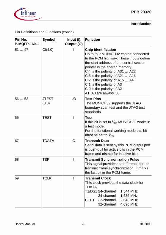
51 … 47 CI(4:0) I Chip IdentificationUp to four MUNICH32 can be connected to the PCM highway. These inputs define the start address of the control section pointer in the shared memory.CI4 is the polarity of A31 … A22CI3 is the polarity of A21 … A16CI2 is the polarity of A15 … A4CI1 is the polarity of A3CI0 is the polarity of A2A1, A0 are always ‘00’
56 … 53 JTEST(3:0)
I/O Test PinsThe MUNICH32 supports the JTAG boundary scan test and the JTAG test standards.
65 TEST I TestIf this bit is set to VDD MUNICH32 works in a test mode.For the functional working mode this bit must be set to VSS.
67 TDATA O Transmit DataSerial data is sent by this PCM output port is push-pull for active bits in the PCM frame and tristate for inactive bits.
68 TSP I Transmit Synchronization PulseThis signal provides the reference for the transmit frame synchronization. It marks the last bit in the PCM frame.
69 TCLK I Transmit ClockThis clock provides the data clock for TDATAT1/DS1 24-channel 1.544 MHz
24-channel 1.536 MHzCEPT 32-channel 2.048 MHz
32-channel 4.096 MHz
Pin Definitions and Functions (cont’d)
Pin No.P-MQFP-160-1
Symbol Input (I)Output (O)
Function
User’s Manual 20 01.2000
PEB 20320
Introduction
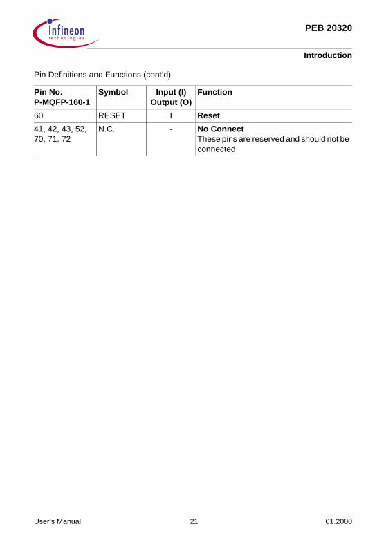
60 RESET I Reset
41, 42, 43, 52, 70, 71, 72
N.C. - No ConnectThese pins are reserved and should not be connected
Pin Definitions and Functions (cont’d)
Pin No.P-MQFP-160-1
Symbol Input (I)Output (O)
Function
User’s Manual 21 01.2000

PEB 20320
Introduction
1.4 Logic Symbol
Figure 2MUNICH32 Logic Symbol
ITL03488
SerialInterface
(3:0)BE
1)
A31/DP3, A30/DP2, A29/DP1, A28/DP0, A[27:2]
(31:0)D
30
32
RCLK
RSP
RDATA
TCLK
TSP
TDATA
I/M
W/R R/W
ADS/AS
DS/PCHK
READY/DSACK
BERR
B16
HOLD/BR
HLDA/BG
BGACK/PM
HLDAO/BGO
AR
INT/INT
5 (4:0)CI
4TEST
JTEST (3:0)
RESET
SCLK
VDD
VSS
InterfaceSystem
BusMicroprocessor
Interface
MUNICH32PEB 20320
1)
User’s Manual 22 01.2000

PEB 20320
Introduction
1.5 Functional Block Diagram
Figure 3Block Diagram of MUNICH32
ITB03495
BE (3:0) A (31:2) D (31:0)
32
RCLK RSP RDATATCLK TSP TDATA
I/MW/RADS DS READY/ BERR B16HOLD/ HLDA/ HLDAO/ ARINT/
CI (4:0)
4
TEST JTESTRESET
BGACKAS DSACK BRR/W BG BGO INT
SCLK
5
Microprocessor Bus Interface
Serial Interface/Formatter Controller Unit
CSRConfiguration and
State RAM
CMDMA Controller
FormatterTransmit
TF
TBTransmit Buffer
DeformatterReceive
RD
Receive BufferRB
CD
MI
/PM
User’s Manual 23 01.2000

PEB 20320
Introduction
The internal functions of MUNICH32 are partitioned into 8 major blocks.
1. Serial Interface, Formatter Control Unit CD – Parallel-Serial conversion, PCM timing, switching of the test loops, controlling of the
multiplex procedure.2. Transmit Formatter TF
– HDLC frame, bit stuffing, flag generation, flag stuffing and adjustment,CRC generation, transparent mode transmission and V.110, X.30 80 bit framing.
3. Transmit Buffer TB– Buffer size of 64 long words allocated to the channels, i.e. eight PCM frames can be
stored before transmission, individual channel capacity programmable.4. Receive Deformatter RD
– HDLC frame, zero-bit deletion, flag detection, CRC checking, transparent modereception and V.110, X.30 80 bit framing.
5. Receive Buffer RB– Buffer size of 64 long words allocated to the channels, i.e. eight PCM frames can be
stored, individual long words are freely accessible by each channel.6. Configuration and State RAM CSR
– Since the Transmit Formatter, Receive Deformatter are used in a multiplex manner,the state and configuration information of each channel has to be stored.
7. DMA Controller CM– Interrupt processing, memory address calculation, chaining list handling,
chip configuration.8. µP interface MI
– Motorola/Intel microprocessor interface.
User’s Manual 24 01.2000

PEB 20320
Introduction
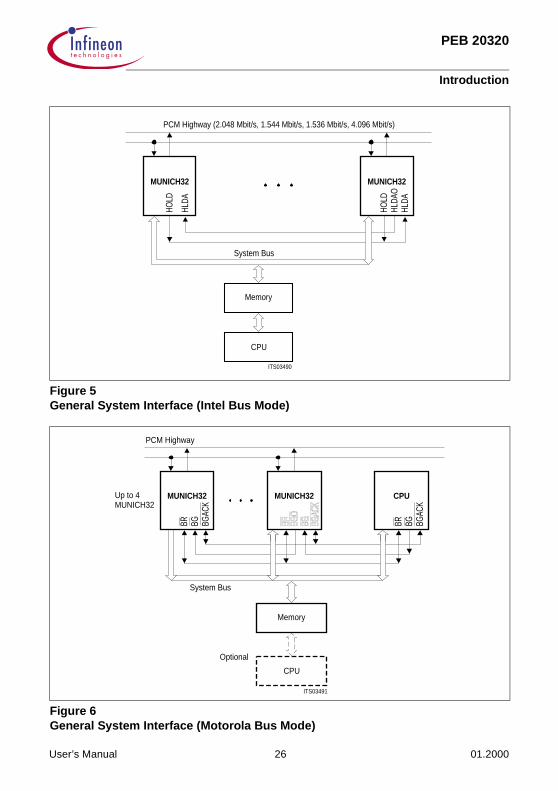
1.6 System Integration
The MUNICH32 is designed to handle up to 32 data channels of a PCM highway. Ittransfers the data between the PCM highway and a memory shared with a hostprocessor via a 32-bit µP interface. At the same time it performs protocol formatting anddeformatting as well as rate adaption for each channel independently. The host sets theoperating mode, bit rate adaption method and time slot allocation of each channel bywriting the information into the shared memory.
Using subchanneling each time slot can be shared between up to four MUNICH32s; sothat in one single time slot four different D-channels can be handled by four MUNICH32s.
Figure 4, Figure 5 and Figure 6 give a general overview of system integration of theMUNICH32.
Figure 4General System Integration (Intel Bus Mode)
ITS03489
MUNICH32
0
HLDA
1
MUNICH32
HLDA
MUNICH32
2
HLDA
3
MUNICH32
HLDA
CPU
Optional
System Bus
Up to 4MUNICH32
PCM Highway (2.048 Mbit/s, 1.544 Mbit/s, 1.536 Mbit/s, 4.096 Mbit/s)
CPU
Memory
HOLD
HLDA
HOLD
HLDA
HLDA
O
HOLD
HLDA
OHL
DA
HOLD
HLDA
OHL
DA
HOLD
HLDA
User’s Manual 25 01.2000
PEB 20320
Introduction
Figure 5General System Interface (Intel Bus Mode)
Figure 6General System Interface (Motorola Bus Mode)
ITS03490
MUNICH32 MUNICH32
Memory
CPU
System Bus
PCM Highway (2.048 Mbit/s, 1.544 Mbit/s, 1.536 Mbit/s, 4.096 Mbit/s)
HOLD
HLDA
HOLD
HLDA
HLDA
O
ITS03491
MUNICH32 MUNICH32 CPU
Optional
System Bus
Up to 4MUNICH32
PCM Highway
CPU
Memory
BR BG BGAC
K
BGAC
KBGBR
User’s Manual 26 01.2000
PEB 20320
Introduction
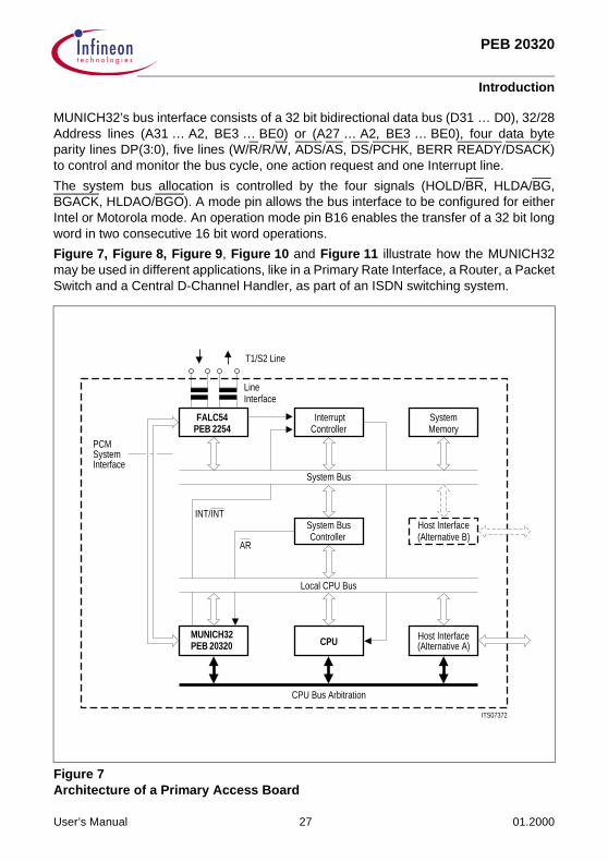
MUNICH32’s bus interface consists of a 32 bit bidirectional data bus (D31 … D0), 32/28Address lines (A31 … A2, BE3 … BE0) or (A27 … A2, BE3 … BE0), four data byteparity lines DP(3:0), five lines (W/R/R/W, ADS/AS, DS/PCHK, BERR READY/DSACK)to control and monitor the bus cycle, one action request and one Interrupt line.
The system bus allocation is controlled by the four signals (HOLD/BR, HLDA/BG,BGACK, HLDAO/BGO). A mode pin allows the bus interface to be configured for eitherIntel or Motorola mode. An operation mode pin B16 enables the transfer of a 32 bit longword in two consecutive 16 bit word operations.
Figure 7, Figure 8, Figure 9, Figure 10 and Figure 11 illustrate how the MUNICH32may be used in different applications, like in a Primary Rate Interface, a Router, a PacketSwitch and a Central D-Channel Handler, as part of an ISDN switching system.
Figure 7Architecture of a Primary Access Board
ITS07372
Host Interface(Alternative B)
System Bus
Local CPU Bus
CPU (Alternative A)
INT/INT
AR
PCMSystemInterface
CPU Bus Arbitration
2254FALC54
PEB ControllerInterrupt
MemorySystem
System BusController
InterfaceLine
T1/S2 Line
20320MUNICH32PEB
Host Interface
User’s Manual 27 01.2000

PEB 20320
Introduction
Figure 8Architecture of a Central D-Channel Handler
ITS04829
EPICPEB 2056
InterruptController
HSCXSAB 82525
System Bus
ControllerSystem Bus
CPUPEB 20320MUNICH32
INT/INT
AR
PCMSystemInterface
Local CPU Bus
CPU Bus Arbitration
MemorySystem
Signaling HighwayPCM Highway
(Alternative B)Host Interface
(Alternative A)
R
Host Interface
User’s Manual 28 01.2000

PEB 20320
Introduction
Figure 9Architecture of a Packet Switch/Router
ITS07374
Controller
System Bus
System Bus
CPU
INT/INT
AR
PCMSystemInterface
Local CPU Bus
CPU Bus Arbitration
Memory
Line Driver
V.24, V.21, V.35, ...
2254FALC54
PEB
Interrupt System
Controller
InterfaceLine
T1/S2 Line
20320MUNICH32PEB
SAB 82538ESCC8
User’s Manual 29 01.2000

PEB 20320
Introduction
Figure 10MUNICH32 in a System with a RISC CPU
Note: To reduce complexity the host interface is not explicitly shown here.
ITS07371
InterruptController
SystemMemory
System Bus
ControllerSystem Bus
CPU
Motorola 68020)with Intel 386 or
(not compatible
INT/INT
AR
PCMSystemInterface
LineInterface
T1/S2 Line
Local CPU BusLocal CPU Bus
CPU Bus ArbitrationCPU Bus Arbitration
FALC54PEB 2254
MUNICH3220320PEB
User’s Manual 30 01.2000

PEB 20320
Introduction
Figure 11MUNICH32 in a System using Multiport Memory
Note: To reduce complexity the host interface is not explicitly shown here.
ITS07373
System Bus
ControllerMulti Port RAM
CPU
INT/INT
AR
Local CPU BusLocal CPU Bus
CPU Bus ArbitrationCPU Bus Arbitration
System Bus
MemoryMulti Port
20320MUNICH32PEB
2254FALC54
PEB ControllerInterrupt
MemorySystem
Controller
InterfaceLine
T1/S2 Line
InterfaceSystemPCM
User’s Manual 31 01.2000

PEB 20320
Functional Description
2 Functional Description
2.1 Serial Interface
The serial interface of MUNICH32 includes a data receive (RDATA) and a data transmitline (TDATA) as well as the accompanying control signals (RCLK = Receive Clock,RSP = Receive Synchronization Pulse, TCLK = Transmit Clock, TSP = TransmitSynchronization Pulse). The timings of the receive and transmit PCM highway areindependent of each other, i.e. the frame positions and clock phases are not correlated.Data is transmitted and received either at a rate of 2.048 Mbit/s for the CEPT 32-ChannelEuropean PCM format (Figure 14) or 1.544 Mbit/s or 1.536 Mbit/s for theT1/DS1 24-Channel American PCM format (Figure 12 and Figure 13). MUNICH32 mayalso be connected to a 4.096-Mbit/s PCM system (Figure 15), where it handles eitherthe even- or odd-numbered time slots, so all 64 time slots can be covered by connectingtwo MUNICH32s to the PCM highway.
The actual bit rate of a time slot can be varied from 64 Kbit/s down to 8 Kbit/s for thereceive and transmit direction. A fill mask code specified in the time slot assignmentdetermines the bit rate and which bits of a time slot should be ignored. Any of thesetime slots can be combined to a data channel allowing transmission rates from 8 Kbit/sup to 2.048 Mbit/s.
The frame alignment is established by the transmit and receive synchronization pulse(TSP, RSP), respectively. The sampled rising edge of TSP identifies the current bit onthe serial line (TDATA) as the last bit of a PCM frame. The sampled rising edge of RSPindicates that the current bit on the serial line (RDATA) is the first bit of a PCM frame.
The F-bit for the 1.544 MHz T1/DS1 24-channel PCM format is ignored in receivedirection, the corresponding bit is tristate in transmit direction. It is therefore assumedthat this channel is handled by a different device.
For test purposes four different test loops can be switched. In a complete loop all logicalchannels are mirrored either from serial data output to input (internal loop) or vice versa(external loop).
In a channelwise loop one single logical channel is logically mirrored either from serialdata output to input (internal loop) or vice versa (external loop).
A detailed description of the different loops is found in Chapter 4.2.1 and Chapter 5.1.
User’s Manual 32 01.2000

PEB 20320
Functional Description
Figure 12 T1/DS1 Mode PCM Frame Timing 1.544 MHz
Note 1: A box in a bit of the RDATA line means that this bit is ignored (HDLC,TMB, TMR, V.110/X.30) or received as ‘1’-bit (TMA; one overwrite).
Note 2: The fill/mask bit for the F-bit is not defined. TDATA is tristate for the F-bit, andthe F-bit is ignored in the receive direction.
Note 3: TSP and RSP must have one single rising and falling edge during a125 µs PCM frame.
ITD03496
T1/DS1 - Mode Receive Frame Timing 1 1 0 1 0 1 1 0
Fill/Mask : Slot 0
Fill/Mask : Slot 0
1 0 0 1 1 0 0 0T1/DS1 - Mode Transmit Frame Timing
TCLK
TSP
TDATA
FILL/MASK
0SLOT 23SLOT 1SLOT 0
125 µs
PCM - Frame
SLOT 0 SLOT 1SLOT 23
1 2 3 4 5 6 7 0 1 2 3 4 5 6 7F
7 F 0 1 2 3 4 5 6 7
76543210F7
SLOT 23 SLOT 1SLOT 0
FILL/MASK
RDATA
RSP
RCLK
DATA DATA DATA DATA DATA DATA
6
6
User’s Manual 33 01.2000

PEB 20320
Functional Description
Figure 13T1/DS1 Mode PCM Frame Timing 1.536 MHz
Note 1: A box in a bit of the RDATA line means that this bit is ignored (HDLC,TMB, TMR, V.110/X.30) or received as ‘1’-bit (TMA; one overwrite).
Note 2: TSP and RSP must have one single rising and falling edge during a125 µs PCM frame.
ITD03497
T1/DS1 - Mode Receive Frame Timing 1 1 0 1 0 1 1 0
Fill/Mask : Slot 0
Fill/Mask : Slot 0
1 0 0 1 1 0 0 0T1/DS1 - Mode Transmit Frame Timing
TCLK
TSP
TDATA
FILL/MASK
0SLOT 23SLOT 1SLOT 0
125 µs
PCM - Frame
SLOT 0 SLOT 1SLOT 23
1 2 3 4 5 6 7 0 1 2 3 4 5 6 7
7 0 1 2 3 4 5 6 7
SLOT 23
FILL/MASK
RDATA
RSP
RCLK
DATA DATA DATA DATA DATA DATA
6
6 765432107
SLOT 1SLOT 0
User’s Manual 34 01.2000

PEB 20320
Functional Description
Figure 14CEPT Mode PCM Frame Timing
Note 1: A box in a bit of the RDATA line means that this bit is ignored (HDLC,TMB, TMR, V.110/X.30) or received as ‘1’-bit (TMA; one overwrite).
Note 2: TSP and RSP must have one single rising and falling edge during a125 µs PCM frame.
ITD03498
CEPT - Mode PCM - Frame Timing 1 1 0 1 0 1 1 0
Fill/Mask : Slot 0
Fill/Mask : Slot 0
1 0 0 1 1 0 0 0CEPT - Mode Transmit Frame Timing
TCLK
TSP
TDATA
FILL/MASK
0SLOT 31SLOT 1SLOT 0
125 µs
PCM - Frame
SLOT 0 SLOT 1SLOT 31
1 2 3 4 5 6 7 0 1 2 3 4 5 6 7
7 0 1 2 3 4 5 6 7
SLOT 31
FILL/MASK
RDATA
RSP
RCLK
DATA
6
6 765432107
SLOT 1SLOT 0
DATADATADATADATA DATA DATA
User’s Manual 35 01.2000

PEB 20320
Functional Description
Figure 154.096 Mbit/s PCM Frame Timing
Note 1: A box in a bit of the RDATA line means that this bit is ignored (HDLC,TMB, TMR, V.110/X.30) or received as ‘1’-bit (TMA; one overwrite).
Note 2: TSP and RSP must have one single rising and falling edge during a125 µs PCM frame.
ITD03528
0 1 2 3 4 5 6 7
SLOT 0 SLOT 1
76543210
SLOT 31
76543210
125 µs
TSP
RSP
4.096 Mbit/s PCM-format: even numbered slot allocation
4.096 Mbit/s PCM-format: odd numbered slot allocation
RSP
TSP
0 1 2 3 4 5 6 7
SLOT 31
0 1 2 3 4 5 6 7
SLOT 0
76
User’s Manual 36 01.2000
PEB 20320
Functional Description
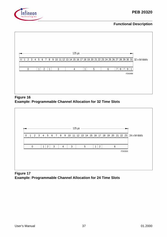
Figure 16Example: Programmable Channel Allocation for 32 Time Slots
Figure 17Example: Programmable Channel Allocation for 24 Time Slots
ITD03499
125 µs
0
0
32 x 64 kbit/s1 2 3 4 5 6 7 8 9 10 11 12 13 14 15 16 17 18 19 20 21 22 23 24 25 26 27 28 29 30 31
1 2 1 3 4 1 5 6 7 8 7 9 1
ITD03500
125 µs
0 1 2 3 4 5 6 7 8 9 10 11 12 13 14 15 16 17 18 19 20 21 22 23
0 1 2 3 4 5 1 2 63
24 x 64 kbit/s
User’s Manual 37 01.2000
PEB 20320
Functional Description
2.2 Microprocessor Interface
A 64-channel DMA controller (32 channels in receive direction and 32 channels intransmit direction) with buffer chaining capability is integrated in the MUNICH32. Itprovides DMA functions for up to 32 full duplex channels and allows data transferbetween the serial interface and an external memory. The MUNICH32 performs longword by long word transfers on a 32-bit bidirectional data bus (D(31:0)) and addressesup to 4 GByte of RAM with a 30-bit address bus (A(31:2)). The chip always works as asystem bus master and can be operated in either a Intel or Motorola environment.MUNICH32 receives commands and data from the host processor via the sharedmemory. The host stores the action specification containing configuration initializationand monitor commands in the memory. Afterwards the host informs the MUNICH32 bygenerating an action request pulse (AR line). The MUNICH32 reacts by reading theaction specification and informs the microprocessor by appending the respectiveinterrupt information to the interrupt queue. In addition, the INT/INT line is activatedduring the write access belonging to the interrupt specification.
The timing of the microprocessor interface is established according to the Intel 80386 orMotorola 68020 processor. The system clock (SCLK) provides the fundamental timingfor the µP interface and is the internal device clock. Each bus cycle performs a long word(B16 = 1) or a word (B16 = 0) transfer and takes four system clock periods in the fastestcase, any number of wait clock cycles can be inserted.
MUNICH32’s architecture is based on a 32-bit data structure. Therefore MUNICH32performs long word operations preferably. While the word operation mode is selected thelong word operation is divided into two consecutive word operations. In the case of aread access the data of the two words are connected together to build a 32-bit long wordbefore processing.
For a read access first the MSB bytes of a long word will be transferred and then theLSB bytes via D(15:0).For a write access first the LSB-bytes of a long word will be transferred and then theMSB bytes via D(15:0).The signal B16 cannot be changed dynamically and should be set to ‘1’ in Intel paritymode (parity mode is not available in 16-bit word Intel mode).
Mode Operation Mode B16 BE(3–0) Access
Intel
Motorola
1 0 0
1 0 0
0H 3H CH
0H 8H AH
long wordMSB wordLSB word
long wordMSB wordLSB word
User’s Manual 38 01.2000

PEB 20320
Functional Description
2.2.1 Intel Mode
The Intel mode has two submodes – parity mode (even parity) and non parity mode – tobe chosen by strapping PM to ‘1’ or ‘0’ respectively.
In Intel mode the lower (higher) ordered byte of a long word (D31 … D0) is assigned tothe lower (higher) ordered physical address.
The read or write bus cycle is controlled by the signals W/R, ADS and READY as shownin Figure 18, Figure 19. Each bus cycle consists of two bus states (S1, S2). During stateS1 the address signals and bus cycle definition signals are driven valid. Simultaneously,the address status ADS is asserted to indicate their availability. The bus cycles areterminated by asserting READY. READY is ignored on the first bus state S1 andsampled at the end of the following state S2. If READY is not asserted in S2 then waitcycles SW are inserted until a bus cycle end is detected. During a read cycle theMUNICH32 floats its data signals to allow external memory to drive the data bus.
The input data and parity bits DP3–0 (if parity mode is selected) is latched when READYis asserted. During a write cycle MUNICH32 drives the data signals and parity bits DP3–0 (if parity mode is selected) beginning in the second clock period of S1 until the firstclock period following the cycle acknowledgment READY. If a bus cycle error indicatedby BERR has occurred, the MUNICH32 terminates the bus cycle. In case of a read cyclein the control and configuration section an action request fail interrupt is generated andthe action is suspended. In case of a read cycle in the transmit data section thecorresponding frame is aborted and a FO interrupt is generated. In all other cases of reador write cycles terminated with an error condition no actions are performed.
A 4-bit data byte parity bus DP3–0 is used in Intel mode if parity mode is selected bystrapping PM to ‘1’. During a read access DP3–0 is supposed to contain the parity ofD(31:24), D(23:16), D(15:8) and D(7:0) respectively. A low active output PCHK indicateswhether the parity was correct (PCHK = 1) or wrong (PCHK = 0) in the clock cycle afterthe data/parity is latched. PCHK stays low 1 or 2 clock cycles. No further action is takenas consequence to a parity fail.
As the memory access is performed by using one common system bus, busmanagement is done with the signals HOLD, HLDA and HLDAO as shown in Figure 20.
The wired or HOLD line is driven high whenever one of the MUNICH32s has to performa bus transfer. The activated HOLD ACKNOWLEDGE indicates that the bus control willbe released. If the specific device has activated the HOLD itself, it will start the memoryaccess. Otherwise it will pass the signal to the next cascaded device. Several memoryaccesses may be required if the MUNICH32 has not been granted access recently.In this example of four MUNICH32 devices sharing the same bus,each device will generate four memory cycles, giving a total of 16 cycles perHOLD/HLDA/HLDAO tenure. In order to prevent blocking in the case of continuousrequest by one device, the MUNICH32 does not generate another HOLD REQUESTbefore the HOLD ACKNOWLEDGE has been deactivated.
User’s Manual 39 01.2000

PEB 20320
Functional Description
If the HOLD ACKNOWLEDGE is driven low while the MUNICH32 is performing a buscycle, the bus is released later than two clock periods after de-assertion of HOLDACKNOWLEDGE. The current bus cycle is finished with a bus cycle error. This actionshould be followed by an ASP.RES as described in Chapter 4.2.1.
Figure 18Read Cycle Timing Diagram (Intel mode)
ITD03501
S1 S2 S1 S2 S1 S2SW WSREAD READ BERR
SCLK
BE(3:0)
W/R
ADS
READY
[DP3-DP0], D(31:0)
BERR
Tristate
A31-A2
[A27-A2]
[PCHK]
User’s Manual 40 01.2000

PEB 20320
Functional Description
Figure 19Write Cycle Timing Diagram (Intel mode)
ITD03502
WRITE WRITE BERR
SCLK
BE(3:0)
W/R
ADS
READY
[DP3-DP0], D(31:0)
BERR
Tristate
A31-A2
[A27-A2]
INT
[PCHK]
User’s Manual 41 01.2000

PEB 20320
Functional Description
Figure 20Bus Management for Intel Bus Mode
Note 1: Bus Cycle means, that the MUNICH32 under consideration starts a read orwrite access at most 4 clock periods after HLDA is asserted after its HOLD. TheMUNICH32 terminates the cycle typically two clock periods after the lastbus cycle.
Note 2: In the Bus Management example it is assumed that the MUNICH32 underconsideration has a higher priority than the other bus master. HOLD (internal) istherefore the internal request generated by the MUNICH32, HOLD (external)the signal on the external HOLD line, being the OR combination of the HOLDsignal generated by the MUNICH32 and the other bus master(s).
Note 3: A typical configuration example for a system with several bus masters is givenin Figure 4 and Figure 5.
ITD03503
SCLK
HOLD (extern)
HOLD (intern)
HLDA
HLDAO
Bus CycleMax. 4 Clock Periods
~ ~~~
MUNICH32gets the Bus gets the Bus
Another Bus MasterrequestsNo Bus
TristateTristate
Tristate Tristate
User’s Manual 42 01.2000

PEB 20320
Functional Description
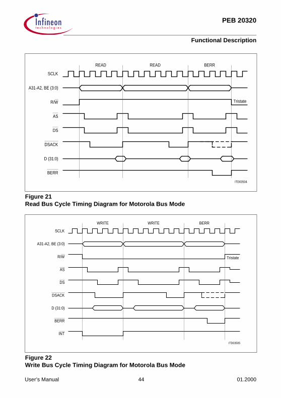
2.2.2 Motorola Mode
In Motorola mode the bus is used in an asynchronous manner. The bus operation usesthe handshake lines (AS, DS, DSACK and BERR) to control data transfer as shown inFigure 21, Figure 22. Address strobe AS indicates the validity of an address on theaddress bus (A31 … A2) and of the bus definition R/W (Read or Write cycle). It isasserted half a clock cycle after the beginning of a bus cycle. The data strobe DS signalis used as a condition for valid data of a write cycle. MUNICH32 asserts DS one full clockcycle after the assertion of AS during a write cycle. The data is placed on the bidirectionaldata bus (D31 … D0) half a clock cycle after AS is driven low. For a read cycle,MUNICH32 asserts DS to signal the external memory to drive the data on the bus. DSis asserted at the same time as AS during a read cycle. The data is latched with the lastfalling edge of the clock for that cycle.
The bus cycle is terminated if the data transfer acknowledge (DSACK) is asserted withthe falling edge of the third clock period. Otherwise MUNICH32 inserts wait cycles untilDSACK is recognized. AS and DS are driven high half a clock period before bus cycleend.
The bus error BERR is also a bus cycle termination indicator. It can be used in theabsence as well as in conjunction with DSACK. If an abnormal termination has occurredduring a read cycle, MUNICH32 generates an interrupt and aborts the correspondingtransmit channel. For a write cycle no further action is performed.
As the MUNICH32 is used in a multi-bus-master application, bus arbitration has to bedone to avoid simultaneous system bus access by more than one master. In Motorolamode the bus arbitration protocol of the 68020 is established using the signals BR, BG,BGACK and BGO as shown in Figure 23. The wired-or Bus Request (BR) is driven lowto indicate to the processor that one of the MUNICH32s requires control of the bus. Theactivated Bus Grant (BG) signals the availability of the system bus. If the MUNICH32 hasactivated the bus request itself, it asserts the wired-or Bus Grant Acknowledge toindicate that it has assumed bus mastership. Otherwise it will pass the BUS GRANTsignal to the device cascaded next (BGO). At the same time it releases the Bus Request.After finishing the last bus cycle, the Bus Grant Acknowledge is deactivated and the BusGrant is passed on. In order to prevent blocking in the case of continuous request by onedevice, MUNICH32 does not generate another Bus Request before the external BusRequest and Bus Grant Acknowledge have been deactivated.
After getting the bus mastership MUNICH32 drives the bus and starts the first bus cycleone clock after assertion of BGACK. After finishing the memory access it releases thebus and de-asserts BGACK at the same time.
User’s Manual 43 01.2000
PEB 20320
Functional Description
Figure 21Read Bus Cycle Timing Diagram for Motorola Bus Mode
Figure 22Write Bus Cycle Timing Diagram for Motorola Bus Mode
ITD03504
READ READ BERR
SCLK
A31-A2, BE (3:0)
R/W
AS
DSACK
D (31:0)
BERR
Tristate
DS
ITD03505
WRITE WRITE BERR
SCLK
A31-A2, BE (3:0)
R/W
AS
DSACK
D (31:0)
BERR
Tristate
DS
INT
User’s Manual 44 01.2000

PEB 20320
Functional Description
Figure 23Bus Management for Motorola Mode
Note: 1. In the Bus Management example it is assumed that the MUNICH32 underconsideration has a higher priority than the other bus master. BR and BGACKare wired AND lines to be pulled to ‘1’ by an external signal.
2. A typical configuration example for a system with several bus masters is givenin Figure 6.
ITD03506
SCLK
BR (extern)
BR (intern)
BGACK (extern)
BGACK (intern)
BGO
BG
Max. 4 Clock Periods
~ ~~~
MUNICH32gets the Bus gets the Bus
Another Bus Master No Busrequests
User’s Manual 45 01.2000

PEB 20320
Functional Description
2.2.3 DMA Priorities
Prioritization of Queueing DMA Cycles
The MUNICH32 will perform all pending accesses on the same bus tenure.
Note: Several bus transactions may be required if the MUNICH32 has not been givenaccess to the system bus for a long period of time. This is often seen in multi-master systems where several MUNICH32 devices share the system bus.
Priority Interrupt
Highest priority Receive link list including accesses to the descriptors
Transmit link list including accesses to the descriptors
Lowest priority Configuration of a channel (action requests)
User’s Manual 46 01.2000

PEB 20320
Functional Description
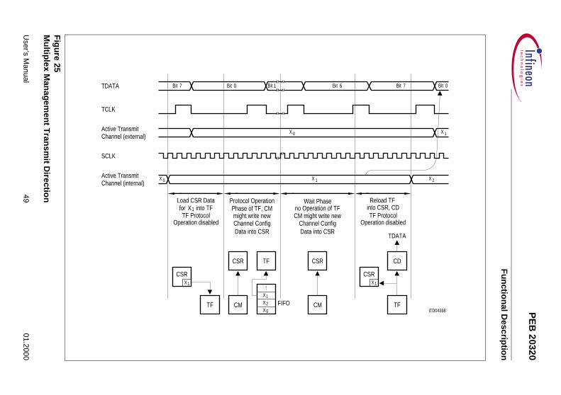
2.3 Basic Functional Principles
MUNICH32 is a Multichannel Network Interface Controller for HDLC, offering a varietyof additional features like subchanneling, data channels comprising of one or moretime slots, DMI 0, 1, 2 transparent or V.110/X.30 transmission and programmable rateadaption. MUNICH32 performs formatting and deformatting operations in any networkconfiguration, where it implements, together with a microprocessor and a sharedmemory, the bit oriented part (flag, bit stuffing, CRC check) of the layer 2 (data linkprotocol level) functions of the OSI reference model.
The block diagram is shown in Figure 3. MUNICH32 is designed to handle up to 32 datachannels of a 1.536/1.544 Mbit/s T1/DS1 24-channel, 2.048-Mbit/s CEPT 32-channel ora 4.096-Mbit/s 32-channel PCM highway. The device provides transmission for all bitrates from 8 Kbit/s up to 2.048 Mbit/s of packed data in HDLC format or of data in atransparent format supporting the DMI mode (0, 1, 2) or V.110/X.30 mode. Tristating ofthe transmission line as well as switching a channelwise or complete loop are alsopossible. An on-chip 64-channel DMA generator controls the exchange of data andchannel control information between the MUNICH32 and the external memory.
The MUNICH32 processes receive and transmit data independently for each time slotand transmission direction respectively (blocks TF = Transmit Formatter, RD = ReceiveDeformatter). The frame counters are reset by the rising edges of the RSP or TSP line.The processing units TF and RD work with a multiplex management, i.e. there exists onlyone protocol handler, which is used by all channels in a time sharing manner (seeFigure 24 and Figure 25). The actual configuration, e.g. transmission mode, channelassignment, fill/mask code or state of the protocol handlers is retrieved from theConfiguration and State RAM (CSR) at the beginning of the time slot and reloaded to theCSR at the end. The control unit (CD) controls the access to the CSR and allows writingof reconfiguration information only if the continuous transfer of the configurationinformation between the CSR and the formatters (TF and RD) will not be disturbed. Inreceive direction, 32 unpacked data bits are first accumulated and then stored into anon-chip receive buffer (RB) for transfer to the shared memory. As soon as the RBreceives 32 bits for a channel it requests access to the parallel microprocessor bus. Theon-chip transmit buffer (TB) is always kept full of data ready for transmission. The TB willrequest more data when 32 bits become available in the ITBS. These buffers allows aflexible access to the shared memory in order to prevent data underflow (Tx) and dataoverflow (Rc).
The transmit buffer (TB) has a size of 64 long words (= 256 bytes). In this buffer, data of8 PCM frames can be stored for each data channel. In this case, there are max. 1 msbetween access to the shared memory and data supply to the Transmit Formatter. Inorder to meet these requirements a variable and programmable part of the buffer (ITBS)must be allocated to each data channel (see Figure 26).
User’s Manual 47 01.2000

PE
B 20320
Fu
nctio
nal D
escriptio
n
User’s M
anual 48
01.2000
Fig
ure 2
Mu
ltiple
1Bit
for into RDLoad CSR DataReload RD
into CSR
X 3
2X
2X
CSRX
Operation disabledRD ProtocolProtocol
eration disabled
SRX1
RD
RDATA
CD
2
RD
ITD04397
4x Man
agem
ent R
eceive Directio
n
RDATA Bit 0 1Bit 2Bit
SCLK
Active
RCLK
(external)ChannelReceive
1X
Channel
ActiveReceive
0X
(internal)
2X
for into RDLoad CD, CSR Data
X1 Phase of RD, CMProtocol Operation
Bit 7Bit ~ ~~~ 0
~~~ ~~~
~~
1X
no Operation of RD,Wait Phase
Operation disabledRD Protocol
Data into CSRChannel Configmight write new
RDATA
CSRCD RD
CSR1X
...
CMRD
CM might write newChannel ConfigData into CSR
CSR
Op
FIFO CM
C
PE
B 20320
Fu
nctio
nal D
escriptio
n
User’s M
anual 49
01.2000
Fig
ure 2
Mu
ltiple
ITD04398
ration disabledF Protocol
to CSR, CDReload TF
X
X
Bit 7 0Bit
R
CD
TF
TDATA
2
1
X1
5x Man
agem
ent T
ransm
it Directio
n
TDATA
TCLK
Active TransmitChannel (external)
SCLK
Active TransmitChannel (internal)
X X
Load CSR Data
TF ProtocolOperation disabled
Protocol OperationPhase of TF, CMmight write newChannel ConfigData into CSR Data into CSR
Channel ConfigCM might write newno Operation of TF
Wait Phase
OpeT
in
X
Bit 7 0Bit Bit 1 Bit 6
CSR
CSR TF
CM
X
...CSR
CMFIFO
CS~ ~
~ ~~ ~ ~~
~~~~
~ ~~ ~
0
10
1
X2
X0
X1
for into TFX1
TF

PEB 20320
Functional Description
For example:a) 2.048-Mbit/s PCM highway
32 × 64-Kbit/s data channels (8 bits are sent with each PCM frame). Two long wordsof the buffer are allocated to each data channel.
b) 1 × 2.048-Kbit/s data channelThe maximum buffer size for one channel (63 long words) is allocated to this datachannel.
c) 6 × 256-Kbit/s and 8 × 64 Kbit/s data channels.Eight long words of the buffer are allocated to each of the 6 data channels with256 Kbit/s and two long words are assigned to each of the 8 data channels with atransmission rate of 64 Kbit/s.
The choice of the individual buffer size of each data channel can be made in the channelspecification (shared memory). The buffer size of one channel is changeable withoutdisturbing the transmission of the other channels.
Figure 26Partitioning of TB
ITD04396
CD
TF
Unused
TB
Active TransmitChannel (internal) Used as Address Offset for TB
ITBS of Channel X 1
64 Long Words0X
X 3
2X
ITBS of Channel
ITBS of Channel
ITBS of Channel
User’s Manual 50 01.2000

PEB 20320
Functional Description
The receive buffer (RB) is a FIFO buffer and also has a size of 64 long words, whichallows storing the data of eight complete PCM frames before transferring to the sharedmemory.Figure 27Partitioning of RB
The data transfer to the shared memory is performed via a 32-bit microprocessorinterface working either in SIEMENS/Intel or Motorola bus mode. Figure 28 shows thedivision of the shared memory required for each MUNICH32:
– Configuration start address located at a programmable address– Control and configuration section– An interrupt circular queue with variable size– Descriptor and data sections for each channel.
ITD04447
64 Long Words
Active ReceiveChannel (internal)
Stored in RB together with Data/Status Word from RD
CD
RD
RB
User’s Manual 51 01.2000

PEB 20320
Functional Description
Figure 28Memory Division for up to four MUNICH32
InterruptQueue
ReceiveDescriptor
DATAReceive Receive
DATA
DescriptorReceive
DescriptorReceive
Channel 31 spec.
Channel 0 spec.
Time-Slot Assignment
INTERRUPT QUEUE Spec.ACTION SPEC.
TransmitDescriptor
DATATransmitTransmit
DATA
DescriptorTransmit
TransmitDescriptor
Control StartAddress
CI(4:0)
Control andConfigurationsection
sectionConfigurationControl and
CI(4:0)
DescriptorTransmit
TransmitDescriptor
DATATransmit Transmit
DATA
DescriptorTransmit
ACTION SPEC.INTERRUPT QUEUE Spec.
Time-Slot Assignment
Channel 0 spec.
Channel 31 spec.
ReceiveDescriptor
ReceiveDescriptor
DATAReceiveReceive
DATA
DescriptorReceive
QueueInterrupt
InterruptQueue
ReceiveDescriptor
DATAReceive Receive
DATA
DescriptorReceive
DescriptorReceive
Channel 31 spec.
Channel 0 spec.
Time-Slot Assignment
INTERRUPT QUEUE Spec.ACTION SPEC.
TransmitDescriptor
DATATransmitTransmit
DATA
DescriptorTransmit
TransmitDescriptor
CI(4:0)
Control andConfigurationsection
sectionConfigurationControl and
CI(4:0)
DescriptorTransmit
TransmitDescriptor
DATATransmit Transmit
DATA
DescriptorTransmit
ACTION SPEC.INTERRUPT QUEUE Spec.
Time-Slot Assignment
Channel 0 spec.
Channel 31 spec.
ReceiveDescriptor
ReceiveDescriptor
DATAReceiveReceive
DATA
DescriptorReceive
QueueInterrupt
ITD03507
Control StartAddress
Control StartAddress
Control StartAddress
Current Receive Descriptor Address 0 ... 31Current Transmit Descriptor Address 31...0
0 ... 31Current Transmit Descriptor Address31...0Current Receive Descriptor Address
Current Receive Descriptor Address 0 ... 31Current Transmit Descriptor Address 31...0
Current Receive Descriptor Address 0 ... 31Current Transmit Descriptor Address 31...0
User’s Manual 52 01.2000

PEB 20320
Functional Description
The shared memory allocated for each transmit and receive channel is organized as achaining list of buffers set up by the host. Each chaining list is composed of descriptorsand data sections. The descriptor contains the pointer to the next descriptor, the startaddress and the size of a data section. It also includes control information like frame endindication, transmission hold and rate adaption with interframe time-fill.
In the transmit direction the MUNICH32 reads a transmit descriptor, calculates the dataaddress, writes the current transmit descriptor address into the CCS, and fills the on-chiptransmit buffer. When the data transfer of the specified section is completed, theMUNICH32 releases the buffer, and branches to the next transmit descriptor. If a frameend is indicated the HDLC, TMB or TMR frame will be terminated and a specified numberof the interframe time-fill byte will be sent in order to perform rate adaption. If frame endis found in a transmit descriptor TMA channel the specified number of programmableTMA flags is appended to the data in the descriptor. If frame end is found in a transmitdescriptor of a V.110/X.30 channel the frame is aborted (after the data in the descriptorare sent) by finishing the current 10-octet frame with ‘zeros’ and sending 2 more 10-octetframes with ‘zeros’ which leads to a loss of synchronism on the peer side. An adjustmentfor the inserted zeros in HDLC is programmable, which leads to a reduction of thespecified number of interframe time-fill by 1/8
th of the number of zero insertions. This canbe used to send long HDLC frames with a more or less fixed data rate in spite of the zeroinsertions. A maskable interrupt is generated before transmission is started again.
User’s Manual 53 01.2000

PEB 20320
Functional Description
The following Sections give Examples of Typical Transmit Situations for the Individual Modes
Variable Size Frame Oriented Protocols (HDLC, TMB, TMR)
Normal operation, handling of frame end (FE) indication and hold (H) indication.
Note: 1. FNUM0 must be set to zero.
2. Flag = 7EH for HDLC00H for TMB, TMR
IC = 7EH for HDLC and IFTF = 0FFH for HDLC and IFTF = 100H for TMB, TMR
3. After sending the FNUM2 – 1 IC characters the device starts polling the hold bitin the transmit descriptor once for each further sent IC character. It also rereadsthe pointer to the next transmit descriptor once with each poll of the holdindication. The pointer to the next transmit descriptor can be changed whileHOLD = 1 is set. The value of the pointer, (read in the poll where HOLD = 0) isused as the next descriptor address. If more than 6 IC characters will be sent,the use of the Transmit Hold (TH) should be considered as an alternative tousing the descriptor hold bit. See Chapter 5.3.2.
User’s Manual 54 01.2000

PEB 20320
Functional Description
Figure 29
ITD0
4446
FE=0
H=
00
=H
1=FE
FE=1
H=
1
Flag
Data
4
..
..
...
Data
1Da
ta 2
Data
3
Tran
smit
Desc
ripto
rs
Data
Sect
ions
...
FNUM
1+1
3Da
ta
Poll
H=1?
Poll
H=0
Next
Tran
smit
Desc
r.De
scr.
Tran
smit
Next
Desc
r.Tr
ansm
itNe
xt
FNUM
0FN
UM1
FNUM
2
Data
4
(Dat
a 1,
Dat
a 2)
Flag
,
FNUM
2..
.
Flag
ΙC,
,CΙ
...Fr
ame
(Fr
ame
)Fr
ame
()
...ΙC
,CΙ
Flag
,CΙ
,Fl
agΙC
,,
CΙCΙ
...,
User’s Manual 55 01.2000

PEB 20320
Functional Description
Fixed Size Frame Oriented Protocols (V110/X.30)
Normal operation, E, S, X change (indicated by the V.110-bit in the transmit descriptor)
Example for TRV = ‘11’
Note: 1. FNUM must be 0 for all transmit descriptors.
2. The actual E-, S-, X-bits have to be in the first transmit descriptor after reset.
3. As shown in the example the contiguous parts of a data section belonging toone descriptor are sent in contiguous frames (DATA 1(1) are the bytes 0 – 3 ofDATA 1, DATA 1(2) are the bytes 4 – 7 of DATA 1). If the end of a data sectionis reached within a frame, the frame is continued with data from the next datasection belonging to a transmit descriptor with the bit V.110 = 0(DATA 2(2) = byte 4 of DATA 2, DATA 3(1) = byte 0 – 2 of DATA 3).
4. The E-, S-, X-bits are only changed from one frame to the next not within aframe. The change occurs in the first frame which does not contain data of theprevious data section.
5. Neither FE nor H may be set to 1 during a normal operation of the mode. Theyboth lead to an abort of the serial interface.
User’s Manual 56 01.2000

PEB 20320
Functional Description
Figure 30
ITD
0444
4
Nex
tTr
ansm
itD
escr
.
NO
=2
V110
=1
FE=0
H =0
0=0
=H
0=FE V1
10
NO
=85=
NO
V110
FE=0
H=
0 =0
1=0
=H
0=FE V1
10
NO
=2
0=0
=H
0=FE V1
10
NO
=9
Fram
e ( E
, S, X
, Dat
a 1
)
(1)
(2)
(1)
(2)
(1)
(2)
..
..
.
...
10 O
ctet
s10
Oct
ets
10 O
ctet
s10
Oct
ets
10 O
ctet
s
E, S
, X,
Dat
a 1
E´, S
´, X´
,
Tran
smit
Des
crip
tors
Dat
aSe
ctio
ns
...00
Des
cr.
Tran
smit
Nex
t
Des
cr.
Tran
smit
Nex
t
Des
cr.
Tran
smit
Nex
t
Des
cr.
Tran
smit
Nex
t
Fram
e ( E
, S, X
, Dat
a 1
)
Fram
e ( E
, S, X
, Dat
a 2
)
Fram
e ( E
, S, X
, Dat
a 2,
D
ata
3
)Fr
ame
( E´,
S´, X
´, D
ata
3
)
Dat
a 2
Dat
a 3
User’s Manual 57 01.2000

PEB 20320
Functional Description
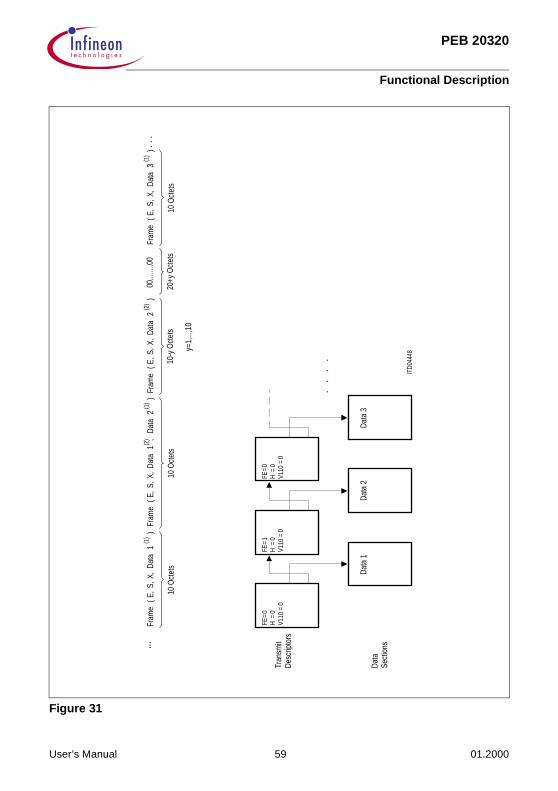
Fixed Size Frame Oriented Protocols (V.110/X.30)
Handling of frame end (FE) indication
Note: 1. FNUM must be ‘0’ for all transmit descriptors.
2. The frame (E, S, X, DATA 2(2)) is the beginning of a 10-octet frame. It stops withthe octet no. y, containing the last data bit of DATA 2 to be sent.
3. Since y = 1, …, 10 the 20 + y times 00H characters sent afterwards cause thepeer station to recognize 3 consecutive 10-octet frames with frame error whichleads to a loss of synchronism in the peer station.
4. For y = 10 DATA 2 is identical to DATA 2(1) and 30 times 00H characters aresent after frame (E, S, X, DATA 1(2), DATA 2(1)).
5. The E-, S-, X-bits are supposed to be loaded by an earlier transmit descriptorin the example. A descriptor changing them (with V.110-bit set) can be putbetween, before or after the descriptors in the example. It will change these bitsaccording to the rules discussed previously.
User’s Manual 58 01.2000
PEB 20320
Functional Description
Figure 31
ITD0
4448
V110
FE=0
H=
0 =0
0=0
=H
1=FE V1
10V1
10
FE=0
H=
0 =0
Fram
e(
(1)
)Fr
ame
((2
))
00,..
....,0
02
Data
Data
3)
(1)
(Fr
ame
..
..
...
10 O
ctet
s10
-y O
ctet
s20
+y O
ctet
s10
Oct
ets
Data
1Da
ta 2
Data
3
Tran
smit
Desc
ripto
rs
Data
Sect
ions...
E,S,
X,
10 O
ctet
s
,X,
S,E,
(1)
2Da
taDa
ta1
Fram
e(
(2)
)
y=1,
...,1
0
1Da
taE,
S,X,
E,S,
X,
User’s Manual 59 01.2000

PEB 20320
Functional Description
Fixed Size Frame Oriented Protocols (V110/X.30)
Handling of hold (H) indication
Figure 32
ITD0
4449
V110
FE=0
H=
0 =0
0=1
=H
1=FE V1
10V1
10
FE=0
H=
0 =0
Fram
e(
(1)
)Fr
ame
((2
))
00,..
....,0
02
Data
Data
3)
(1)
(Fr
ame
..
..
...
10 O
ctet
s10
-y O
ctet
s20
+y O
ctet
s10
Oct
ets
Data
1Da
ta 2
Data
3
Tran
smit
Desc
ripto
rs
Data
Sect
ions
...E,
S,X,
10 O
ctet
s
,X,
S,E,
(1)
2Da
taDa
ta1
Fram
e(
(2)
)
y=1,
...,1
0
0000
...00
00
Poll
H=1?
Poll
H=0
E,S,
X,1
Data
E,S,
X,
User’s Manual 60 01.2000
PEB 20320
Functional Description
Time Slot Oriented Protocol (TMA)
Normal operation, handling of frame end (FE) indication and hold (H) indication.
Note: 1. FNUM must be set to zero.
2. TC = FFH for TMA and FA = 0the programmed flag with TMA and FA = 1
3. After sending the FNUM2 – 1 IC characters the device starts polling the hold bitin the transmit descriptor once for each further sent IC character. It also rereadsthe pointer to the next transmit descriptor once with each poll of the holdindication. The pointer to the next transmit descriptor can be changed whileHOLD = 1 is set. The value of the pointer, (read in the poll where HOLD = 0) isused as the next descriptor address. If more than 6 IC characters will be sent,the use of the Transmit Hold (TH) should be considered as an alternative tousing the descriptor hold bit. See Chapter 5.3.2.
User’s Manual 61 01.2000

PEB 20320
Functional Description
Figure 33
ITD0
4445
FE=0
H=
00
=H
1=FE
FE=1
H=
1
TCDa
ta 4
..
..
...
Data
1Da
ta 2
Data
3
Tran
smit
Desc
ripto
rs
Data
Sect
ions
...
FNUM
1+1
Data
3TC
, TC,
TC,
......
..TC,
TC
Poll
H=1?
Poll
H=0
Next
Tran
smit
Desc
r.De
scr.
Tran
smit
Next
Desc
r.Tr
ansm
itNe
xt
FNUM
0FN
UM1
FNUM
2
Data
4
Data
1Da
ta 2
Tim
e-Sl
otBo
unda
ries
TC,..
......
......
....,T
CTC
, TC,
......
......
.TC,
FNUM
2..
.
...
......
....
..
User’s Manual 62 01.2000

PEB 20320
Functional Description
An activated transmission hold (hold bit in descriptor) prevents the MUNICH32 fromsending more data. If a frame end has not occurred just before, the current frame will beaborted and an interrupt generated. Afterwards, the interframe time-fill bytes will beissued until the transmission hold indication is cleared. There is a further transmit hold(TH) bit in the Channel Specification (CCS) in addition to the hold bit in the descriptor.Setting the transmit hold (TH) bit by issuing a channel command will prevent furtherpolling of the transmit descriptor (see Chapter 5.3.2).
This hold bit (CCS.TH) is interpreted in the CD; it causes the transmit formatter to stayin the idle state and to send interframe time-fill after finishing the current frame. In thecase of a very short frame (< ITBS), this frame will stay in the TF and not be sent untilCCS.TH is removed. (In case of X.30/V.110 the current frame is aborted).
This means that the buffer TB is not emptied from the TF side after the current frame,but still requests further data from the shared memory until it is filled. In the case of thedescriptor hold on the other hand, the TF empties the TB and there are no further datarequests from the shared memory until the descriptor hold is withdrawn. Then TB is filledagain and the TF is activated only after enough data are provided in the TB to prevent adata underrun.
The Reaction to the Transmit Hold Bit is now Discussed for the Different Modes in the Following Sections
Variable Size Frame Oriented Protocols (HDLC, TMB, TMR)
Reaction to a channel specification containing TH = 1
Normal operation
Note: 1. IC = 7EH for HDLC and IFTF = 1FFH for HDLC and IFTF = 000H for TMB or TMR
2. flag = 7EH for HDLC00H for TMB or TMR
3. FNUM2 is ignored. The number of interframe time-fills sent between the firstframe and the second frame solely depends on the AR low pulse leading to theaction with the channel with TH = 0.
4. The times ∆t1 and ∆t2 are statistical but typically only a few clock cycles.
5. The TH bit (as all channel commands) is not synchronized with TB! (asopposed to the H-bit in the descriptor) TH acts on the frame currently beingsent, not necessarily on the last frame currently stored in the TB. In theexample, TB may or may not have stored DATA 3 before the action requestwith TH = 1 was issued. See Chapter 4.2.5 for a further discussion of thisissue.
6. If TH is handed over to CD outside of a frame, TH = 1 prevents the MUNICH32from sending the next frame.
User’s Manual 63 01.2000

PE
B 20320
Fu
nctio
nal D
escriptio
n
User’s M
anual 64
01.2000
Fig
ure 3
Data 3 ...Frame ( ), Flag
0handed over from CM to CDin the Channel Specification
4
ITD04450
FE=0H = 0
Flag
. . . .
Data 1 Data 2
...
..., 1Data Flag, Ι C,( )Frame CΙ
∆ t 1 ∆ t 2
TH=1 TH=in the Channel Specificationhanded over from CM to CD
AR
....
. . . .
, Data 2
Data 3
FNUM20=H1=FE

PEB 20320
Functional Description
Fixed Size Frame Oriented Protocol (V.110/X.30)
Reaction to a channel specification containing TH = 1
Normal operation
Note: 1. The times ∆t1 and ∆t2 are statistical but typically only a few clock cycles.
2. The current frame processed, when TH = 1 is handed over to CD is aborted,only 10 – y, (y = 1, …, 10) octets of it are sent. The device then starts to send20 + y 00H characters no matter how fast the TH bit is withdrawn. This ensures,that the peer site is informed about the abort with a loss of synchronism
3. The data section DATA 1 is split in the example; DATA 1(1) is sent in theaborted frame, all bits that were read into the MUNICH32 with the same accessare discarded (they would have been sent in the next frame(s) if TH = 1 wasnot issued) and the device starts the next frame with the bits DATA 1(3) of theaccess to DATA 1 that follows the one getting the bits of DATA 1(1).
4. The TH (as all channel commands) is not synchronized with TB. TH acts onthe frame currently sent, not necessarily on the last stored data.
5. If TH is handed over to CD before a frame has started after an abort or afterreset no frame will start.
User’s Manual 65 01.2000

PEB 20320
Functional Description
Figure 35
Time Slot Oriented Protocol (TMA)
Reaction to a channel specification containing TH = 1
Note: 1. TC is the programmed TFLAG for FA = 1FFH for FA = 0
2. The times ∆t1 and ∆t2 are statistical but typically only a few clock cycles.
3. The TH bit (as all channel commands) is not synchronized with the TB! (asopposed to the H-bit in the descriptor) TH acts to the data stream currently sent.
ITD04454
FE=0H = 0
. . . .
...
Data 1
...
10-y Octets
1Data ...
∆ t1TH=1 in theChannel
AR
Frame ( )(1) 00
Specificatonhanded overfrom CM to CD
00 0000 ..............
Channelin theTH=0
2t∆
10 Octets
1DataFrame ( )(3)
20+y Octets
...
from CM to CDhanded overSpecificaton
E, S, X, E, S, X,
User’s Manual 66 01.2000

PE
B 20320
Fu
nctio
nal D
escriptio
n
User’s M
anual 67
01.2000
Fig
ure 3
Data 3 ...TC,
=0handed over from CM to CDin the Channel Specification
6
ITD04452
FE=0H = 0
. . . .
Data 1 Data 2
...
FNUM0
1Data TC, ,TCTC,
∆ t 1 ∆ t 2
TH=1 THin the Channel Specificationhanded over from CM to CD
AR
, ....Data 2 ,
Data 3
Time-Slot Boundaries
==FE
H 01

PEB 20320
Functional Description
Variable Size Frame Oriented Modes (HDLC, TMB, TMR)
Reaction to a channel specification containing TH = 1
Silencing of poll cycles for hold.
Note: An AR pulse for an action specification leading to TH = 1 should be issued after(ITBS + 2) polls of the MUNICH32, where ITBS is the previously programmednumber of long words in the TB reserved for this channel.
User’s Manual 68 01.2000

PE
B 20320
Fu
nctio
nal D
escriptio
n
User’s M
anual 69
01.2000
Fig
ure 3
Data 2 ...
PollH=0
. . .
Frame ( )CΙ , Flag...,
0handed over from CM to CDin the Channel Specification
7
ITD04451
FE=1H = 1
Flag
. . . .
Data 1 Data 2
...
FNUM0
PollH=1?
FNUM0
..., 1Data Flag, Ι C, , CΙ...( )Frame Ι C, ,CΙ CΙ,
PollH=1?
Ι ,C ...
No Poll
...
CΙ ,
∆ t 1 ∆ t 2
TH=1 TH=in the Channel Specificationhanded over from CM to CD
AR
....
. . . .

PEB 20320
Functional Description
Fixed Size Frame Oriented Protocol (V110/.30)
Silencing of poll cycles by TH = 1
Note: 1. The times ∆t1 and ∆t2 are statistical but typically only a few clock cycles.
2. The TH bit (as all channel commands) is not synchronized with TB! (asopposed to the H-bit in the descriptor) TH acts to the data stream currently sent.
3. In the example the proper use to silence a channel polling the HOLD bit of thetransmit descriptor is illustrated. The AR pulse is issued after the polling hasstarted and the H-bit is not reset before polling has stopped by the TH bit.
4. An AR pulse for an action specification leading to TH = 1 should be issued after(ITBS + 2) polls of the MUNICH32, where ITBS is previously programmednumber of long words in the TB reserved for this channel.
User’s Manual 70 01.2000

PE
B 20320
Fu
nctio
nal D
escriptio
n
User’s M
anual 71
01.2000
Fig
ure 3
...
CDr
10 Octets
2DataFrame ( )(1)E, S, X,
8
ITD04455
FE=1H = 1
. . . .
Data 1 Data 2
...
10 Octets
1Data ...
PollH=1
∆ t 1
TH=1in theChannel
AR
Frame ( )(1) (2) )(Frame Data 1
10-y Octets
00
Specif.handedover to CD
H=1No Poll
H=1 H=0Poll
00 0000 ..............
from CM to handed oveSpecif.Channelin theTH=0
2t∆
20+y Octets
E, S, X, E, S, X,

PEB 20320
Functional Description
Time Slot Oriented Protocol (TMA)
Reaction to a channel specification containing TH = 1
Note: 1. TC = FFH for TMA and FA = 0the programmed flag for TMA and FA = 1
2. FNUM2 is ignored. The number of interframe time-fills between the first frameand the second frame solely depends on the AR low pulse leading to the actionwith the channel with TH = 0.
3. The times ∆t1 and ∆t2 are statistical but typically only a few clock cycles.
4. The TH bit (as all channel commands) is not synchronized with TB (asopposed to the H-bit in the descriptor) TH acts on the data stream currently sentnot necessarily on the last data stored in TB. In the example TB may or maynot have stored DATA 3 before action request with TH = 1 was issued.
5. The data stream is stopped and TC sent after the last byte of DATA 2 is sent.The stopping is triggered by the FE = 1 bit in the descriptor.
6. If TH is bonded over to CD during interframe time-fill (TC) it prevents theMUNICH32 from sending further data afterwards.
7. An AR pulse for an action specification leading to TH = 1 should be issued after(ITBS + 2) polls of the MUNICH32, where ITBS is previously programmednumber of long words in the TB reserved for this channel.
User’s Manual 72 01.2000

PE
B 20320
Fu
nctio
nal D
escriptio
n
User’s M
anual 73
01.2000
Fig
ure 3
Data 2 ...
PollH=0
. . .
TC,C ...,
0handed over from CM to CDin the Channel Specification
9
ITD04453
FE=1H = 1
. . . .
Data 1 Data 2
...
FNUM0
PollH=1?
FNUM0
... 1Data TC, , TC... TC, ,TC T,
PollH=1?
,TC ...
No Poll
...
TC,
∆ t1 ∆ t2
TH=1 TH=in the Channel Specificationhanded over from CM to CD
AR
, ,TC ....
. . . .

PEB 20320
Functional Description
In receive direction the MUNICH32 reads a receive descriptor, calculates the dataaddress, writes the current receive descriptor address into the CCS, and exchanges databetween the on-chip receive buffer and the external memory. After the data section hasbeen filled, the MUNICH32 writes the number of stored bytes (BNO) into the descriptor.If a frame end has occurred the frame status is written into the descriptor and an interruptis generated. The frame status includes the CRC check results and transmission errorinformation like ‘non octet of bits’, ‘aborted frame’, ‘data overflow’, ‘maximum framelength exceeded’ and ‘frames with less than or equal to two data bytes’. An activatedreception-hold in the descriptor prevents the MUNICH32 from processing the receivedata. The incoming frames are discarded until the hold is deactivated.
Because the MUNICH32 is divided into two non-synchronized parts by the on-chipbuffers, two different kinds of aborting a channel transmission are implemented.
– Normal abort:This abort of a receive or transmit channel is processed in theformatters of the serial interface. The interframe time-fill code is sent after aborting thecurrent issued frame. No accesses to the on-chip buffers are carried out, until theabort is withdrawn. The handling of the link lists and the processing of the buffers bythe DMA controller are not affected by normal abort.
– Fast abort: A fast abort is performed by the DMA controller and does not disturb thetransmission on the serial interface. If this abort is detected the current descriptor issuspended with an abort status immediately followed by a branching to the newdescriptor defined in the channel specification of the CCS.
For initialization and control the host sets up a Control and Configuration Section (CCS),including the action specification, interrupt queue specification, time slot assignment andthe channel specification. The host initiates an action, e.g. reconfiguration, change of thechannel mode, reset or switching of a test loop by updating the CCS and issuing anaction request pulse. When the action request pulse is detected by the MUNICH32 itreads the control start address, then the action specification and, if necessary, additionalinformation from the CCS. After execution, the action request is acknowledged by aninterrupt.
MUNICH32 indicates an interrupt by activating the interrupt line and storing the interruptinformation including the corresponding channel number in the interrupt queue. Theinterrupt queue is a circular buffer; MUNICH32 starts to write the interrupt queuespecification and fills it successively in a circular manner. The host has to allocatesufficient buffer size and to empty the buffer fast enough in order to prevent overflow ofthe queue.
User’s Manual 74 01.2000

PEB 20320
Functional Description
Monitoring functions are implemented in MUNICH32 to discover errors or conditionchanges, i.e.
– Receive frame end– Receive frame abort by overflow of the receive buffer or hold condition or recognized
ABORT flag– Frame overflow, if a frame has to be discarded because of pending inaccessibility of
the chip memory – Transmit frame end– Transmit frame abort (data underrun) by underrun of the transmit buffer or hold
condition or bus cycle error– Change of the interframe time-fill.– Loss of synchronism or change of framing bits (V.110, X.30).– Short frame with no data content detected.
An error or condition change is indicated by an interrupt. The host may react to theinterrupt by either aborting or tristating the specific channel or with a channelreconfiguration. To prevent underrun of the transmit buffer sufficient buffer size has tobe allocated to the channel.
A more detailed discussion of the receive procedure with examples is provided under thedetailed protocol description in Chapter 2.4.
User’s Manual 75 01.2000

PEB 20320
Functional Description
2.4 Detailed Protocol Description
In the following sections the protocol support of the MUNICH32 is described in detail fortransmit and receive direction separately.
Each section starts with a discussion of the general features proceeds with protocolvariants and options from the channel specification and closes with a description of theinterrupts and special topics.
HDLC
Transmit Direction General Features
In transmit direction
– the starting and ending flag (7EH before and after a frame)– the interframe time-fill between frames– the zero insertions (a ‘0’-bit after 5 consecutive ‘1’s inserted within a frame)– (optional) the Frame Check Sequence (FCS) at the end of a frame
is generated automatically.
Options
The different options for this mode are
– the kind of the interframe time-fill character in the channel specification– 7EH for IFTF = 0 – FFH for IFTF = 1
– the number of interframe time-fill characters as FNUM in the transmit descriptor. Forthe values FNUM = 0, 1, 2 we have – FNUM = 0 frame 1, 7EH, frame 2 (start flag = end flag)– FNUM = 1 frame 1, 7EH, 7EH, frame 2– FNUM = 2 frame 1, 7EH, IC, 7EH, frame 2
– the correction of the number of interframe time-fill characters by 1/8 of the number ofzero insertions by programming FA in the channel specification.– FA = 0: FNUM from the transmit descriptor is taken directly to determine
the number of interframe time-fill characters as shown in Figure 39.– FA = 1: FNUM from the transmit descriptor is reduced by 1/8 of the
number of the zero insertions of the frame corresponding to thetransmit descriptor as shown in Figure 40. This allows for a more or
less constant bit rate transmission for long HDLC frames.
User’s Manual 76 01.2000

PEB 20320
Functional Description
Figure 40
Note: 1. is the biggest integer smaller than .
1. For FNUM – < 0, y = 0
– the kind of Frame Check Sequence (FCS)two kinds of frame check sequences are implemented by the CRC bit in thechannel specificationCRC = 0: the generator polynomial x16 + 12 + x5 + 1 is used
(2 byte FCS of CCITT Q.921)CRC = 1: the generator polynomial x32 + x26 + x23 + x22 + x16 + x12 + x11 + …
… x10 + x8 + x7 + x5 + x4 + x2 + x + 1(4 byte FCS) is used
– the suppression of the automatic generation of the FCS is programmable inthe channel specification:
– CS = 0: FCS generated automaticallyCS = 1: FCS generation suppressed
and in the transmit descriptorCSM = 0: FCS generated automatically if CS = 0 in the
channel specificationCSM = 1: FCS generation suppressed
ITD04579
FE=1 FNUM
DataContents
ofFrame 1 Frame 2
ofContents
Data
7 EH Frame 1 Frame 2
x ZeroInsertions
HE7 . . . . . . 7 EH
y+1
[ ],max (FNUM - 0)y= x8
x8---
x8---
x8---
User’s Manual 77 01.2000

PEB 20320
Functional Description
Interrupts
The possible interrupts for the mode in transmit direction are:
HI: issued if the HI bit is detected in the transmit descriptor (not maskable)
FI: issued if the FE bit is detected in the transmit descriptor(maskable by FIT in the channel specification)
ERR: one of the following transmit errors has occurred:– the last descriptor had H = 1 and FE = 0– the last descriptor had NO = 0 and FE = 0
(maskable by TE in the channel specification)
FO: one of the following transmit errors have occurred– a BERR = ‘0’ was detected during a read access to a transmit data section for
this channel– the MUNICH32 was unable to access the shared memory in time either for new
data to be sent or for a new transmit descriptor.(maskable by TE in the channel specification)
typical data stream has the form
Example:
HDLC channel withCS = 0) (FCS generated automatically)INV = 0 (no inversion)CRC = 0 (CRC16)TRV = 00 (required as unused in HDLC mode)FA = 1 (flag adjustment)MODE = 11 (HDLC)IFTF = 1 (interframe time-fill ‘1’s)INTEL interfaceChannel number 1A
… ITF FLAG DATA FCS FLAG ITF …
User’s Manual 78 01.2000

PEB 20320
Functional Description
Figure 41
Note: 1. Data is transmitted according to §2.8 of CCITT recommendation Q.921
2. Note: FCS in the data section is formatted as ordinary data!!!
3. FCS is generated here automatically as CS = 0 and CSM = 0 for the1st descriptor.
4. There was 1 zero insertion in the 1st frame, so FNUM – = FNUM = 2.Therefore between the first and the second frame we have FLAG ITF FLAG and ITF = FFH because IFTF = 1.
ITD04578
A0010002
AA
031
FFFFFFFF
80060801 80030800
31 0
Generate FI, HI-Int.2000081A
31 0
31 0
31 0
31 0
2000181AGenerate FI-Int.
1DATA
1 Descst nd2 Desc 3 Descrd
0
1
FF
0 0
AddressIncreasesFE=1
HOLD=0HI=1
NO=1CSM=0
FNUM=2 FNUM=1CSM=1
NO=6HI=0
HOLD=0FE=1
01111110..... 01010101 00010100010111110 01111110 11111111
FLAG
Time Increases
FLAG 3ITF
Zero Insertion
FCS 2
5FLAGFLAG
0111111011111011111011111011111011111011111011111011111001111110
DATA 28 Zero Insertion 4
011111100101010100010100010111110
FLAG
Zero Insertion
DATA 3
Generate FI-Int.2000081A
FE=1HOLD=0
HI=0NO=3
CSM=1FNUM=0
00
AAFA 28
00000000
18---
User’s Manual 79 01.2000

PEB 20320
Functional Description
5. No FCS is generated here as CSM is ‘1’ for the second and third transmitdescriptor. The FCS is supposed to be the last 2 bytes to be transmitted in thiscase, their validity is not checked internally.
6. There was 8 zero insertions in the 2nd frame, so FNUM – = FNUM – 1 = 0.Therefore between the second and the third frame we have a shared FLAG.
For CS = 1 (CRC select) the transmitted data stream would differ at FCS, FCS would justbe omitted.
For INV = 1 (channel inversion) all bits of the data stream (including FLAG, DATA, FCS,ITF) would be inverted.
For CRC = 1 (CRC 32) the transmitted data stream would only differ in the FCS, the FCSwould be 1101 0111 1010 0101 1000 0000 0010 0111.
For FA = 0 (no flag adjustment) the transmitted data stream would change only afterDATA 2. The value FNUM = 1 in the second descriptor would alone determine thenumber of interframe time-fill characters, the scenario would look like
Figure 42
For IFTF = 0 (ITF flags) the transmitted data stream would only differ at ITF, the 8 oneswould be replaced by 0111 1110.
For Motorola interface the only difference is in the data section
For the first descriptor it ought to be
and for the second
and for the third
31 0
AA
31 0
FF FF FF FF
FF 00
31 0
AA 28 FA
88---
DATA 2 FLAG FLAG DATA 3
0111 111 0111 111
User’s Manual 80 01.2000

PEB 20320
Functional Description
HDLC
Receive DirectionGeneral Features
In receive direction:
1. The starting and ending flag (7EH before and after a frame) is recognized and extracted.
2. A change of the interframe time-fill is recognized and reported by an interrupt.3. The zero insertions (a ‘0’-bit after five ‘1’s within a frame) are extracted.4. The FCS at the end of a frame is checked, it is (optionally) transferred to the shared
memory together with the data.5. The number of the bits within a frame (without zero insertions) is checked to be
divisible by 8.6. The number of bytes within a frame is checked to be smaller than MFL + 1 (after
extraction of ‘0’ insertions).7. The number of bits within a frame after extraction of ‘0’ insertions is checked
to be greater than (case NSF = 0 only)
8. The occurrence of an abort flag (7FH) ending a frame is checked.
More detailed description of the individual features:
1. a. A frame is supposed to have started if after a sequence of 0111 1110 in the receivedata stream neither FCH nor FDH nor 7EH has occurred. The frame is supposed tohave started with the first bit after the closing ‘0’ of the sequence.
b. A frame is supposed to have stopped if a sequence of 0111 1110 or 0111 1111 isfound in the data stream after the frame has started. The last bit of the frame issupposed to be the bit preceding the ‘0’ in the above sequences. The cases ofsequences 0111 1110 1111 111 and 0111 1110 0111 1111 are also supposed tobe frames of bit length – 1 and 0 respectively. A frame is also supposed to have stopped if more than MFL bytes were receivedsince the start of the frame and it wasn’t stopped yet.
c. The ending flag of a frame may be the starting flag of the next frame (shared flagssupported).
(case NSF = 0 only) check a) 16 for CRC = 0
32 for CRC = 1
(only for CS = 0) check b) 32 for CRC = 0
48 for CRC = 1
(case NSF = 1 & CS = 1 only) check a’) 8 for CRC = x (ignored)
User’s Manual 81 01.2000

PEB 20320
Functional Description
2. The receiver is always in one of two possible interframe time-fill states:to be called F and O.The following diagram explains them.A change from F to O and from O to F is reported by an IFC interrupt.
Figure 43
3. The ‘0’ extraction is also carried out for the last 6 bits before the stopping sequence.4. The last 16 (CRC = 0) or 32 (CRC = 1) bits of a frame (after extraction of the zero
insertions are supposed to be the FCS of the remaining bits of the frame. (For the caseof a frame with less than or equal to 16 or 32 bits respectively see discussion of 7).The FCS is always checked, the check is reported in the CRCO bit of the last receivedescriptor of the frameCRCO = 1: FCS was incorrectCRCO = 0: FCS was correct.
5. The check is reported in the NOB bit in the last receive descriptor of the frameNOB = 1: The bit length of the frame was not divisible by 8.NOB = 0: The bit length of the frame was divisible by 8.If NOB = 1: The last access to a receive data section of the frame may containerroneous bits and shouldn’t be evaluated.
6. The check is reported in the LFD bit in the last receive descriptor of the frame.LFD = 1: The number of bytes was greater than MFL.LFD = 0: The number of bytes was smaller or equal to MFL.Only the bytes up to the
MFL + 1st one for CS =1MFL – 1st one for CS = 0, CRC = 0MFL – 3rd one for CS = 0, CRC = 1
are transferred to be stored memory. The bytes of the last access may be erroneousand shouldn’t be evaluated.
ITD04577
RESET or Receive OFF
O
F
Receive InitializeChannel Command
111111111111111in the Data Stream(15 contiguous "1"sreceived) or aReceive Abort ChannelCommand during 15received Bitssupported)
shared Zerosreceived, Flags with(2 contiguous Flagsin the Data Stream0111111001111110011111101111110 or
User’s Manual 82 01.2000
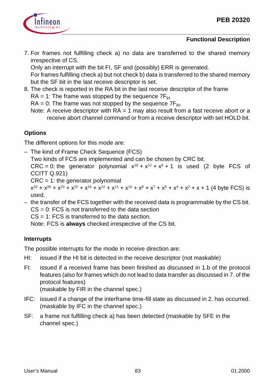
PEB 20320
Functional Description
7. For frames not fulfilling check a) no data are transferred to the shared memoryirrespective of CS.Only an interrupt with the bit FI, SF and (possibly) ERR is generated.For frames fulfilling check a) but not check b) data is transferred to the shared memorybut the SF bit in the last receive descriptor is set.
8. The check is reported in the RA bit in the last receive descriptor of the frameRA = 1: The frame was stopped by the sequence 7FHRA = 0: The frame was not stopped by the sequence 7FH.Note: A receive descriptor with RA = 1 may also result from a fast receive abort or a
receive abort channel command or from a receive descriptor with set HOLD bit.
Options
The different options for this mode are:
– The kind of Frame Check Sequence (FCS)Two kinds of FCS are implemented and can be chosen by CRC bit.CRC = 0: the generator polynomial x16 + x12 + x5 + 1 is used (2 byte FCS ofCCITT Q.921)CRC = 1: the generator polynomial x32 + x26 + x23 + x22 + x16 + x12 + x11 + x10 + x8 + x7 + x5 + x4 + x2 + x + 1 (4 byte FCS) isused.
– the transfer of the FCS together with the received data is programmable by the CS bit.CS = 0: FCS is not transferred to the data sectionCS = 1: FCS is transferred to the data section.Note: FCS is always checked irrespective of the CS bit.
Interrupts
The possible interrupts for the mode in receive direction are:
HI: issued if the HI bit is detected in the receive descriptor (not maskable)
FI: issued if a received frame has been finished as discussed in 1.b of the protocolfeatures (also for frames which do not lead to data transfer as discussed in 7. of theprotocol features) (maskable by FIR in the channel spec.)
IFC: issued if a change of the interframe time-fill state as discussed in 2. has occurred.(maskable by IFC in the channel spec.)
SF: a frame not fulfilling check a) has been detected (maskable by SFE in the channel spec.)
User’s Manual 83 01.2000

PEB 20320
Functional Description
ERR: issued if one of the following error conditions has occurred:– FCS was incorrect– the bit length was greater than MFL– the frame was stopped by 7FH– the frame could only be partly stored because of internal buffer overflow of RB– a fast receive abort channel command was issued– a receive abort channel command was detected during reception of a frame – a frame could only be partly transferred to the shared memory because of a
receive descriptor with HOLD bit set (maskable by RE in the channel spec.)
FO: issued if due to inaccessibility of internal buffer RB– one ore more complete frames have been lost– one ore more changes of interframe time-fill state were lost
(maskable by RE in the channel spec.)
Example:
HDLC channel withCS = 1 (FCS transferred to shared memory)INV = 0 (no inversion)CRC = 1 (CRC 32)TRV = 00 (required as unused in HDLC mode)FA = x (irrelevant)MODE = 11 (HDLC)IFTF = x (irrelevant)Motorola interfaceChannel No. 1DMFL = 10
User’s Manual 84 01.2000

PEB 20320
Functional Description
Figure 44
ITD04576
031
20080000
031
nd2 Desc
40080000
8800203D
C0031C00
1 Descst
000C0000
31 0
Last Access ofa LFD Frame
Generate HI-Int.
031CRCO,NOB,
Generate FI, ERR-Int.8800123D
should be Ignored
C2 A1 01 03
39 80 3D BC
DATA 2
LFD
4
..... 01111110 1000 0101 1000 0000 1100 0000 1001 1100 0000 00010100 0011
11010011 0100001010111101001101101000001111100001110111100
01111111
1FLAG DATA 1, FCS 1
2 DATA Ignored up to next Flag
Abort Sequence 3
5
User’s Manual 85 01.2000

PEB 20320
Functional Description
Figure 45
ITD04575
031
200C0000
031
rd3 Desc
C0080000
8800303D
C0081800
4 Descth
000C0000
31 0
Last Access ofa NOB Frame
Generate FI, HI-Int.
031
FB49AC00CRCO,NOB
Generate FI, ERR-Int.8800123D
should be Ignored
00 AC 49 FB
C0 A4 F2 FA
DATA 2
FCS 2
DATA 3
01111110 0011 0101 1001 0010 1101 1111 00000 0000
FLAG DATA 2
6
2FCS
00110000 0111101011111010001010010
0011 0101 1001 0010 1101 1111 00000 0000
DATA 3FLAG
01111110
0010 0101 0100 1111 0101 11110000 0011
FCS 3
01111110
FLAG
Zero Insertion
(shared)
Zero Insertion
Zero Insertion
Zero Insertion Missing
User’s Manual 86 01.2000

PEB 20320
Functional Description
Figure 46
Note: 1. After Receive Initialization is detected all data are ignored until a flag isreceived. The receiver is in the interframe time-fill state ‘0’.
2. After MFL + 1 data bytes are received the further data are ignored (except fora change of the interframe time-fill state) and are neither stored in the RB norreported to the shared memory. The receiver waits for the next flag.
3. Even the abort sequence at the end of the frame will not lead to the RA bit inthe descriptor to be set.
4. Data are formatted according to §2.8 of CCITT Q.921.
5. The FCS is formatted as ordinary data!!!
ITD04574
000C0000
AA 7B A5 01
031
01A57BAA
00140000
31 0
(15 1)8800083D
31 0
31 0
8800143D
Generate short
FCS 4
5 Descth th6 Desc
C0050200C0050000
RA8
1 1111
DATA Ignored up to next Flag 7 15
E4 XX XX XXXXXXXXE4
10
DATA 4
Generate IFC-Int.
8800083D
Generate IFC-Int.8800123D
8800103DGenerate FI-Int.
Generate FI, ERR-Int.(2 Flags)
9
FrameInterrupt for FCS 5 *
11
1111110101000110011100111010 0111 011101111 1111
x "1"
5
1010 0101 1000 0000 0010 01111101 1110
DATA 4
5FCS
00000000 000000000000000000000000
0101 0101
FCS 4
0111 1110 111 1110
2 Flags with shared 0 FLAG
01111110
01010101
6DATA
01111110
FLAG FCS 6
01111111
Abort Sequence
1101 1110 1010 0101 1000 0000 0010 0111
Generate Short Frame Interrupts8800163D8800163D
011111100011111101111111 12
User’s Manual 87 01.2000

PEB 20320
Functional Description
6. LFD is issued and always accompanied by NOB.CRCO shouldn’t be interpreted for a LFD frame.
7. Here the ending flag of the second frame is the starting flag of the third frame.
8. After an abort sequence data is ignored until a flag is found (except for achange of the interframe time-fill state). They are neither stored in the RB norreported to the shared memory.
9. The last 3 bytes in the last write access to the receive data section of the 5thdescriptor have to be ignored.
10.The 2 flags with a shared 0 in the middle change the original interframe time-fill state ‘0’ of the receiver to ‘F’. The 2 flags following FCS 5 on the other handdo not change the interframe time-fill state, as it already was ‘F’.
11.The frame consisting only of 32 times 0 between 2 flags does not passcheck a). It only leads to an interrupt.
12.The 15 × ‘1’ leads to a change of the interframe time-fill state from ‘F’ to ‘0’ eventhrough it is in a data ignored zone.
13.This frame of length – 1 leads to an interrupt.
For CS = 0 (CRC not select) the descriptor would have looked like
Figure 47
ITD04572
031
20080000
031
0301A1C2
st1 Desc
C0071C00
HI,8800323D 8800303D
Generate HI,
C0040000
Desc3 rd
00 AC 49 FB
31 0
200C0000
31 0
Last Access of a LFD Frameshould be Ignored
2
FI-Int.Generate
FI, ERR-Int.
1
User’s Manual 88 01.2000

PEB 20320
Functional Description
Figure 48
Note: 1. Only the 7 leading bytes are reported (the last 4 are supposed to be the FCSeven in this case).
2. It is assumed here for convenience that the first descriptor points to the thirdand not to the second descriptor as in the original example.
For INV = 1 (channel inversion) all bits of the data stream (including DATA, FCS, flag,abort sequence 15 × ‘1’) are interpreted inversely. e.g. ‘1000 0001’ would be interpretedas flag 15 × ‘0’ would lead to a change from interframe time-fill state ‘F’ to ‘0’ etc.
ITD04573
031
000C0000
031
th4 Desc
C0041800
8800123D
C0014000
5 Descth
000C0000
31 0
C0014200
6 Descth
AA XX XX XX
31 0
00140000
31 0
SF
Last Access of a NOB Frameshould be Ignored
Generate FI, ERR-Int.
031
XXXXXXAACRCO, NOB SF, RA
Interrupts as inthe original Example
User’s Manual 89 01.2000
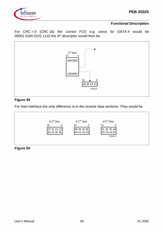
PEB 20320
Functional Description
For CRC = 0 (CRC 16) the correct FCS e.g. zeros for DATA 4 would be00001 0100 0101 1110 the 5th descriptor would then be
Figure 49
For Intel interface the only difference is in the receive data sections. They would be
Figure 50
ITD04570
031
000C0000
031
XXFA28AA
th5 Desc
C0034000
ITD04571
03 01 A1 C2
031
FB 49 AC 00
31 0 031
AA7BA501
1st Desc 3 rd Desc th5 Descof of of
XX XX XX E4C0A4F2FA398030BC
User’s Manual 90 01.2000
PEB 20320
Functional Description
TMB
Transmit DirectionGeneral Features
In transmit direction:
– The starting and ending flag (00H before and after a frame)– The interframe time-fill between frames
is generated automatically.
Options
The different options for this mode are:
– The number of interframe time-fill characters as shown in Figure 26 by choosingFNUM in the transmit descriptor. For the values FNUM = 0, 1, 2 we have
FNUM = 0 … frame 1, 00H, frame 2 … (start = end flag)FNUM = 1 … frame 1, 00H, 00H, frame 2 …FNUM = 2 … frame 1, 00H, 00H, 00H, frame 2 …
Interrupts
The possible interrupts for the mode in transmit direction are identical to those of HDLC.
A typical data stream has the form
ITF DATA ITF DATA
Example
TMB channel withINV = 0 (no inversion)CRC = 0 (required)TRV = 00 (required)FA = 0 (required)MODE = 01 (TMB)IFTF = 0 (required)Intel interfaceChannel number 5
User’s Manual 91 01.2000

PEB 20320
Functional Description
Figure 51
Note: 1. Data is transmitted according to Q.921 §2.8 and fully transparent.
2. A transmit descriptor with NO = 0 and FE = 1 is allowed, one with NO = 0 andFE = 0 is forbidden.
3. FNUM = 1 leads to 2 FLAGS after DATA 2.
ITD04569
20020000
0
CE AB
031
80000000 80030001
45 23 01
31 0
Generate FI-Interrupt88001005
31 0 31 0
31 0
88002005Generate HI-Interrupt
0
0 024 A0 C80 07 35D00 ..........
DATA 21DATA1
88001005Generate FI-Interrupt
FLAG FLAG
0 0
2 FLAGS
2 3
User’s Manual 92 01.2000
PEB 20320
Functional Description
TMB
Receive DirectionGeneral Features
1. The starting and ending flag (00H before and after a frame) as well as interframe time-fill is recognized and extracted.
2. The number of bits within a frame is checked to be divisible by 8.3. The number of bytes within a frame is checked to be smaller than MFL + 1.4. A frame containing less than 8 bits may be ignored completely by the receiver.
More detailed description of the individual features:
1. a. A frame is supposed to have started if after a sequence ‘0000 0000’ a ‘1’-bit isrecognized. The frame is supposed to have this ‘1’-bit as first bit.
b. A frame is supposed to have stopped if– either a sequence 0000 0000 1 is found in the data stream after the frame has
started– or a sequence 0000 0000 is found octet synchronous (i.e. the first bit of the
sequence 00H is the 8 m + 1st bit since the starting ‘1’-bit of 1.a. for an integer m).
In both cases the last bit before the sequence 00H is supposed to be the last bit of theframe.
2. The check is reported in the NOB bit in the last receive descriptor of the frame.NOB = 1: The bit length of the frame was not divisible by 8.NOB = 0: The bit length of the frame was divisible by 8.
3. The check is reported in the LFD bit in the last receive descriptor of the frame.LFD = 1: The number of bytes was greater than MFL.LFD = 0: The number of bytes was smaller or equal to MFL.Only the bytes up to the MFl + 1st one are transferred to the shared memory. The bytesof the last access to the receive data section of the frame may contain erroneous bitsand shouldn’t be evaluated. LFD is always accompanied by NOB.
Options
There are no options in receive direction for this mode.
User’s Manual 93 01.2000

PEB 20320
Functional Description
Interrupts
The possible interrupts for the mode in receive direction are:
HI: issued if HI bit is detected in the receive descriptor (not maskable).
FI: issued if a received frame has been finished as discussed in 1b) of the protocolfeatures or a receive abort channel command was detected during reception of aframe.(maskable by FIR in the channel spec.)
ERR: issued if one of the following error conditions has occurred– the bit length of the frame was not divisible by 8– the byte length was greater than MFL– the frame could only be partly stored because of internal buffer overflow of RB– a fast receive abort channel command was issued– the frame could only be partly transferred due to a receive descriptor with set
HOLD bit.(maskable by RE in the channel specification)
FO: issued if due to inaccessibility of the internal buffer RB one or more completeframes have been lost. (maskable by RE in the channel spec.)
Example:
TMB channel withINV = 0 (no inversion)CRC = 0 (required)TRV = 00 (required)FA = 0 (required)MODE = 01 (TMB)IFTF = 0 (required)MFL = 7Motorola interfaceChannel No. A
User’s Manual 94 01.2000

PEB 20320
Functional Description
Figure 52
ITD04568
00040000
9D 01 XX XX
031
XXXXXXD3
200C0000 20080000
31 0
Generate FI,8800302A
31 0
31 0
31 0
31 0
8800102AGenerate FI-Int.
DATA 3
1DATA DATA 2
1stDesc Descnd2 3 rd Desc
8800322A
C0020800C0010000C0020000
NOB2
HI-Int. HI,Generate FI, ERR-Int.
Last Access of a NOB Frameshould be Ignored
11110111 01010101 0000 0000 0000 10101101 00101010 0000 0000
DATA Ignoredup to next Framestart
5
FLAG FLAGDATA 5
DATA 4
1000000010111100 0000000 11111110 01111111 11111011 11010101 01001100
10100000
FLAGsynchronous
non octet
4
00000000 10111001 10000000 00000000 00
3
11001011 00000000 10000000
DATA 1 DATA 2 DATA 3FLAG FLAG FLAG
octetsynchronous
octetsynchronous
1
(start) FLAG
User’s Manual 95 01.2000

PEB 20320
Functional Description
Figure 53
Note: 1. After Receive Initialization is detected all data are ignored until the startingsequence 0000 0000 1 is detected.
2. Data are formatted according to §2.8 of CCITT Q.921.
3. The octet synchronous (end) flag of one frame can be part of the (start) flag ofthe next frame. Between DATA 1 and DATA 3 they are identical (shared flagssupported).
4. Here the sequence 0000 0000 1 is detected non-octet synchronously.Therefore the frame belonging to DATA 3 is supposed to have ended non-octetsynchronously (NOB set in the 3rd descriptor).
5. After MFL + 1 data bytes the further data are ignored and are neither stored inthe RB nor reported to the shared memory. The receiver waits for the nextsequence 0000 0000 1 to come.
6. If a receive descriptor is full (4th desc.) the MUNICH32 branches to the nextreceive descriptor (5th desc.) even if no further data are to be given to theshared memory.
ITD04567
031
20080000
031
DFFE7F01DATA 4
th4 Desc
40080000
Generate HI-Int.8800202A 8800122A
C0000C00
Desc5 th
00040000
31 0
8800102AGenerate FI-Int.
C0020000
Desc6 th
B5 54 XX XX
31 0
00FC0000
31 0
LFD,
Last Access of a LFD Frameshould be Ignored
Generate FI,
6
NOB
ERR-Int.
DATA 5
User’s Manual 96 01.2000

PEB 20320
Functional Description
For INV = 1 (channel inversion) all bits of the data stream (including DATA, FLAG) areinterpreted inversely e.g. 1111 1111 0 would be interpreted as starting sequence then.
For Intel interface the only difference is in the receive data sections. They would be
Figure 54
ITD05034
XX XX XX D3
031
DF FE 7F 01
31 0 031
B554XXXX
of 2 Descnd of 4 Descth thof 6 Descstof 1 Desc31 0
9D01XXXX
User’s Manual 97 01.2000

PEB 20320
Functional Description
TMR
Transmit DirectionGeneral Features
In transmit direction
– the starting and ending flag (00 00H or 0 00H between frames) is generatedautomatically.
Options
The different options for this mode are
– the number of interframe time-fill characters as shown in Figure 29 by choosingFNUM in the transmit descriptor. For the values 0, 1, 2 we have
FNUM = 0 … frame 1, 000H, frame 2 …FNUM = 1 … frame 1, 00H, 00H, frame 2 …FNUM = 2 … frame 1, 00H, 00H, 00H, frame 2 …
By choosing FNUM = 0 and setting the last transmitted nibble in the transmit data sectionto 0H frames of effective length n + 1/2 bytes can be sent as required by GSM 08.60.
Interrupts
The possible interrupts for the mode in the transmit direction are identical to those ofHDLC.
A typical data stream has the form
ITF DATA ITF DATA
Example:
TMR channel withINV = 0 (no inversion)CRC = 1 (required)TRV = 00 (required)FA = 0 (required)MODE = 01 (TMR)IFTF = 0 (required)Intel interfaceChannel No. 5
User’s Manual 98 01.2000

PEB 20320
Functional Description
Figure 55
Note: 1. Data is transmitted according to Q.921 §2.8 and fully transparent.
2. A transmit descriptor with NO = 0 and FE = 1 is allowed, one with NO = 0 andFE = 0 is forbidden.
3. FNUM = 1 leads to 2 FLAGS after DATA 2.
ITD04566
20020000
0
0E AB
031
80000000 80030001
45 23 01
31 0
Generate FI-Interrupt88001005
31 0 31 0
31 0
88002005Generate HI-Interrupt
0
0 024 A0 C80 07 05D00 ..........
DATA 21DATA1
88001005Generate FI-Interrupt
FLAG FLAG
0 0
2 FLAGS
2 3
Frame of EffectiveLength 1 Byte/21
User’s Manual 99 01.2000

PEB 20320
Functional Description
TMR
Receive DirectionGeneral Features
1. The starting and the ending flag (00 00H) is recognized. Interframe time-fill, bothcharacters of the starting flag and the last character of the ending flag is extracted.
2. The number of bits within a frame is checked to be divisible by 8.3. The number of bytes within a frame is checked to be smaller than MFL.
More detailed description of the individual features
1. a. A frame is supposed to have started after a sequence of 16 zeros a ‘1’-bit isrecognized. The frame is supposed to have this ‘1’-bit as first bit.
b. A frame is supposed to have stopped if– either a sequence of 16 ‘zeros’ and a ‘one’ is found in the data stream after the
frame has started– or a sequence of 16 zeros is found octet synchronous (i.e. the first bit of the
sequence 00 00H is the 8m + 1st bit since the starting ‘1’-bit of 1.a. for aninteger m).
In both cases the eighth bit of the sequence 00 00H is supposed to be the last bit ofthe frame.
2. The check is reported in the NOB bit in the last receive descriptor of the frame.NOB = 1 the bit length of the frame was not divisible by 8.NOB = 0 the bit length of the frame was divisible by 8.If NOB = 1 the last byte of the last access to a receive data section of the frame maycontain erroneous bits and shouldn’t be evaluated. This does not affect the receptionof frames with n + 1/2 octets
3. The check is reported in the LFD bit in the last receive descriptor of the frame.LFD = 1 the number of bytes was greater than MFL.LFD = 0 the number of bytes was smaller or equal to MFL.MFL + 1st one are transferred to the shared memory. The bytes of the last access tothe receive data section of the frame may contain erroneous bits and shouldn’t beevaluated.LFD is always accompanied by NOB.
User’s Manual 100 01.2000

PEB 20320
Functional Description
Options
There are no options in receive direction for this mode.
Interrupts
The possible interrupts for the mode in receive direction are identical to those of TMB.
Example:
TMR channel withINV = 0 (no inversion)CRC = 1 (required)TRV = 00FA = 0MODE = 01 (TMR)IFTF = 0 (required)MFL = 7Motorola interfaceChannel No. 15
User’s Manual 101 01.2000

PEB 20320
Functional Description
Figure 56
ITD04565
00040000
9D 01 00 XX
031
XXXX00D3
200C0000 00080000
01 00 3D AF
31 0
Generate FI, HI-Int.88003035
31 0
31 0
31 0
31 0
88001035Generate FI-Int.
031
20080000
031
569AFB8FDATA 4
DATA 3
1DATA DATA 2
1stDesc Descnd2 3 rd Desc
th4 Desc
88001235
C0060800C0020000C0030000
03 XX XX XX
NOB
Last Byte ofa NOB Frameshould be Ignored
40080000
Generate HI-Int.88002035 88003235
FI,
C0000C00
Desc5 th
20040000
31 0
88001035Generate FI-Int.
C0030000
Desc6 th
BB 5E 00 XX
31 0
00080000
31 0
LFD,
Last Access of a LFD Frameshould be Ignored
Generate
6
5
NOB
HI, ERR-Int.
Generate FI, ERR-Int.
DATA 5
(end) FLAGsynchronousoctet
5DATA
11011101 01111010 00000000 00000000
4DATA
00000000000000001111111111011011110111011111011111110011
0110101011110001 11011111 010110010000
synchronous FLAGnon octet
00000000
2DATA
000000001100101100000000
2(end) FLAG
00000000
(start) FLAG
.... 00000000 00000000
(start) FLAG
1
octet synchronousFLAG1DATA
3
1000000010111001
000000001100000011110101101111000000000010000000
3DATA
4
up to next FramestartDATA Ignored
0000
octet synchronous
User’s Manual 102 01.2000
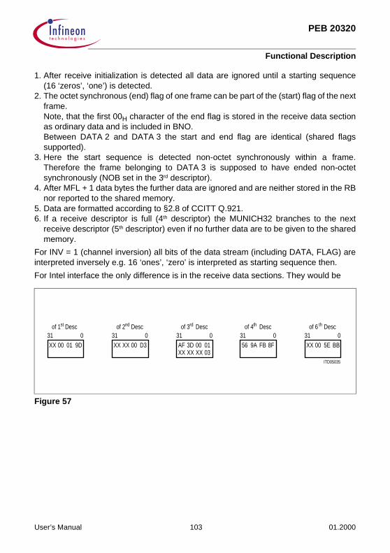
PEB 20320
Functional Description
1. After receive initialization is detected all data are ignored until a starting sequence(16 ‘zeros’, ‘one’) is detected.
2. The octet synchronous (end) flag of one frame can be part of the (start) flag of the nextframe.Note, that the first 00H character of the end flag is stored in the receive data sectionas ordinary data and is included in BNO.Between DATA 2 and DATA 3 the start and end flag are identical (shared flagssupported).
3. Here the start sequence is detected non-octet synchronously within a frame.Therefore the frame belonging to DATA 3 is supposed to have ended non-octetsynchronously (NOB set in the 3rd descriptor).
4. After MFL + 1 data bytes the further data are ignored and are neither stored in the RBnor reported to the shared memory.
5. Data are formatted according to §2.8 of CCITT Q.921.6. If a receive descriptor is full (4th descriptor) the MUNICH32 branches to the next
receive descriptor (5th descriptor) even if no further data are to be given to the sharedmemory.
For INV = 1 (channel inversion) all bits of the data stream (including DATA, FLAG) areinterpreted inversely e.g. 16 ‘ones’, ‘zero’ is interpreted as starting sequence then.
For Intel interface the only difference is in the receive data sections. They would be
Figure 57
ITD05035
XX XX 00 D3
031
56 9A FB 8F
31 0 031
BB5E00XX
nd th thof 1 Descst
31 0
9D0100XX
rd
031
01003DAFXX XX XX 03
of 2 Desc of 3 Desc of 4 Desc of 6 Desc
User’s Manual 103 01.2000
PEB 20320
Functional Description
TMA
Transmit DirectionGeneral Features
In the transmit direction
– a slot-synchronous transparent data transmission– a high impedance overwrite for the masked bits in the slot– a programmable number of programmable fill characters between data
(also slot synchronous)
is generated automatically.
Options
The different options for this mode are
– The value of the fill-character can be programmed for FA = 1 in the channelspecification. The fill-character (TC) is then programmed in the TFLAG. For FA = 0 thefill character is FFH and TFLAG has to be set to 00H. If subchanneling is chosen (notall fill/mask bits of the channel are ‘1’) FA must be set to ‘0’.
– The number of inter-data time-fill characters as shown in Figure 33 by choosingFNUM = 0, 1, 2 we have
FNUM = 0 … DATA 1, TC, DATA 2 …FNUM = 1 … DATA 1, TC, TC, DATA 2 …FNUM = 2 … DATA 1, TC, TC, TC, DATA 2 …
Interrupts
The possible interrupts for this mode in transmit direction are identical to those of HDLC.
User’s Manual 104 01.2000
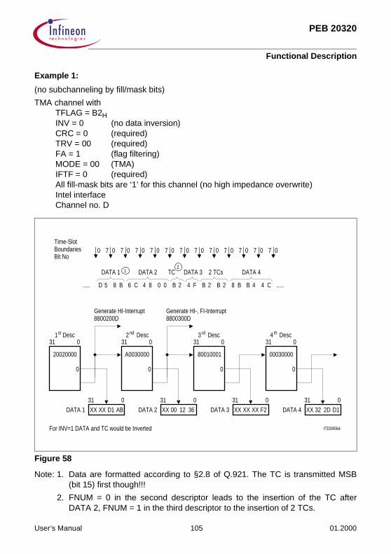
PEB 20320
Functional Description
Example 1:
(no subchanneling by fill/mask bits)
TMA channel withTFLAG = B2HINV = 0 (no data inversion)CRC = 0 (required)TRV = 00 (required)FA = 1 (flag filtering)MODE = 00 (TMA)IFTF = 0 (required)All fill-mask bits are ‘1’ for this channel (no high impedance overwrite)Intel interfaceChannel no. D
Figure 58
Note: 1. Data are formatted according to §2.8 of Q.921. The TC is transmitted MSB(bit 15) first though!!!
2. FNUM = 0 in the second descriptor leads to the insertion of the TC afterDATA 2, FNUM = 1 in the third descriptor to the insertion of 2 TCs.
ITD04564
20020000
0
XX XX D1 AB
031
361200XX
A0030000 80010001
XX XX XX F2
31 0
Generate HI-, FI-Interrupt8800300D
31 0
31 0
31 0
31 0
8800200DGenerate HI-Interrupt
031
00030000
031
D12D32XX
0 0 0
DATA 4DATA 31DATA DATA 2
1st Desc Descnd2 3 rd Desc th4 Desc
4B
0707
4 C8 B
7 0
B 2
7 0
B 2
7 0
4 F
7 0
B 2
7 0
0 0
7 0
4 8
7 0
6 CB85D
7 00BoundariesTime-Slot
Bit No7 0 7 0
..........
DATA 21DATA 4DATADATA 312
TC 2 TCs
For INV=1 DATA and TC would be Inverted
User’s Manual 105 01.2000

PEB 20320
Functional Description
For INV = 1 the data stream would be inverted completely
Figure 59
For FA = 0 TFLAG has to be programmed to 00H and the data stream would be
Figure 60
For Motorola mode the data sections leading to the same data stream would have been
Figure 61
DATA 1 DATA 2 TC DATA 3 2 TCs DATA 4
… 2A 74 93 B7 FF 4D B0 4D 4D 74 4B B3 …
DATA 1 DATA 2 TC DATA 3 2 TCs DATA 4
D5 8B 6C 48 00 FF 4F FF FF 8B B4 4C
ITD05036
36 12 00 XX
031
D1 2D 32 XX
31 0
thof 1 Descst
31 0
XXXXD1AB
rd
031
XXXXXXF2
of 2 Descnd of 3 Desc of 4 Desc
User’s Manual 106 01.2000

PEB 20320
Functional Description
Example 2:
(subchanneling by fill/mask bits)
TMA channel withTFLAG = 00H (required for this case)INV = 0 (no data inversion)CRC = 0 (required)TRV = 00 (required)FA = 0 (required for subchanneling)MODE = 00 (TMA)IFTF = 0 (required)Intel interfaceChannel no. D
Figure 62
ITD04563
20020000
0
XX XX D1 AB
031
361200XX
A0030000 80010001
XX XX XX F2
31 0
Generate HI-Interrupt8800200D
31 0
31 0
31 0
31 0
8800200DGenerate HI-Interrupt
031
00030000
031
D12D32XX
0 0 0
DATA 4DATA 31DATA DATA 2
1st Desc Descnd2 3 rd Desc th4 Desc
User’s Manual 107 01.2000

PEB 20320
Functional Description
Figure 63
Note: Example 2 uses the same descriptors as example 1. Those bits in the data streamthat are at places where fill/mask is ‘zero’ are overwritten by ‘Z’ i.e. highimpedance. In all other protocols bits of the data stream are not overwritten byfill/mask zero bits.Instead the whole data stream is sent at fill/mask one bits for all other protocols.
ITD0
4562
01
23
45
67
Slot
Bou
ndar
ies
Fill/
Mas
kH
igh
Imp.
Ove
rwrit
e
Exte
rnal
Dat
a
Inte
rnal
Dat
a
11
10
11
1
11
11
11
Z1
11
01 1
01
00
1
76
54
32
10
76
54
32
10
76
54
32
10
76
54
32
10
76
54
32
10
Bit N
o
10
11
11
1
Z
1
00
00
Z0
1
111
1111
11
10
01
0Z
DAT
A3
(4F)
B4(8
B4
DAT
ATC
s4C
)
11
10
0
00
ZZ
11
11
1
00
11
11
11
11
11
11
11
11
11
10 Z
10
10
01
1
ZZ
Z1
11
10
11
11
11
11
11
00
01
11
11
0
11
11
11
1
00 0
00
000
0
1
(FF
FF)
2
ITD0
4561
01
23
45
67
Slot
Bou
ndar
ies
Fill/M
ask
High
Imp.
Ove
rwrit
e
Exte
rnal
Dat
a(T
DATA
)
Inte
rnal
Dat
a
10
10
10
00
00
11
11
11
11
Z1
10
1Z
10
ZZ
1Z
01
10
01
0 11
01
01
01
10
11
10
10
10
0
01
11
76
54
32
10
76
54
32
10
76
54
32
10
76
54
32
10
76
54
32
10
Bit N
o
11
10
10
1
0
11
11
1
00
0
00
00
0
00
0
ZZ
ZZ
ZZ
Z01
11
00
00
00
00
0
Z0
10
ZZ
Z0
00
00
0
1 1111
111
111
111
1111
10
0
01
1
0Z
Z
DATA
1(D
58B
)48
(6C
2DA
TATC
(FF)
00)
User’s Manual 108 01.2000

PEB 20320
Functional Description
TMA
Receive DirectionGeneral Features
In the receive direction
– a slot synchronous transparent data reception– a ‘1’ overwrite for masked bits in the slot– for FA = ‘1’ a slot synchronous programmable flag extraction
is performed automatically.
Options
The different options for this mode are:
– the programmable character TC to be extracted for FA = ‘1’ is TFLAG. For FA = ‘0’nothing is extracted. If subchanneling is chosen (not all fill/mask bits of the channelare ‘1’) FA must be set to ‘0’.
Interrupts
The possible interrupts for the mode in receive direction are:
HI: issued if the HI bit is detected in the receive descriptor (not maskable).
ERR: issued if a fast receive abort channel command was issued.(maskable by RE in the channel spec.)
FO: issued if data could only partially stored due to internal buffer overflow of RB.(maskable by RE in the channel spec.)
Example 1:
(no subchanneling)
TMA channel withTFLAG = D7INV = 0 (no channel inversion)CRC = 0 (required)TRV = 00 (required)FA = 1MODE = 00 (TMA)IFTF = 0Motorola interfaceChannel No. E
User’s Manual 109 01.2000
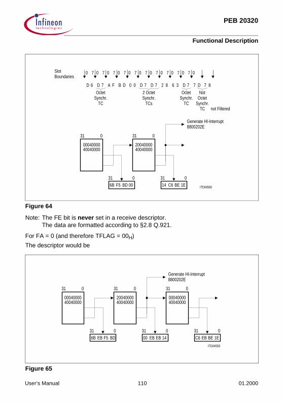
PEB 20320
Functional Description
Figure 64
Note: The FE bit is never set in a receive descriptor.The data are formatted according to §2.8 Q.921.
For FA = 0 (and therefore TFLAG = 00H)
The descriptor would be
Figure 65
ITD04560
0004000040040000
6B F5 BD 00
031
1EBEC614
4004000020040000
31 0
Generate HI-Interrupt8800202E
31 0
31 0
SlotBoundaries
0 07
D 6 D 7 FA
07
DB
07
00
07
7D
07
7D
07
82
07
36
07
7D 87
7 0 7 0
7 D
OctetSynchr.
TC TCsSynchr.2 Octet
TCSynchr.Octet Not
OctetSynchr.
TC not Filtered
ITD04559
0004000040040000
6B EB F5 BD
031
14EBEB00
4004000020040000 00040000
40040000
C6 EB BE 1E
31 0
Generate HI-Interrupt8800202E
31 0
31 0
31 0
31 0
User’s Manual 110 01.2000

PEB 20320
Functional Description
For INV = 1 the receiver filters the inverse of the TFLAG as TC out of the data streamand inverts the data (only the octet synchronous 28H would be filtered).
For Intel interface the data sections would be
for the first descriptor and
for the second.
Example 2:
(with subchanneling)
TMA channel withTFLAG = 00H (required because of subchanneling)INV = 0 (no channel inversion)CRC = 0 (required)TRV = 00 (required)FA = 0 (required because of subchanneling)MODE = 00 (TMA)IFTF = 0Motorola interfaceChannel No. E
00 BD F5 6B
1E BE C6 14
User’s Manual 111 01.2000

PEB 20320
Functional Description
Figure 66
ITD04558
1 1
0004000040040000
00 EF F7 D6
031
1 1 1 1 1 1 0 1 0 0 1 1 0 0 0 1 0 1 1 0 0 0 1 0 1 1 1 1 0 1
Slot Boundaries
Fill/Mask"one" Overwrite
External Data(RDATA)
Internal Data
For INV=1
100101001001011101100110
1111111
101111011011 011111111
00000000
0 0 0 0 0 0 0 0 1 1 1 0 1 1 1 1 0 1 1 1 0 1 10 0
11 0 1 1 1 1 0 1 1 0
31 0
User’s Manual 112 01.2000

PEB 20320
Functional Description
V.110/X.30
Transmit DirectionGeneral Features
In transmit direction
– the synchronization pattern for V.110/X.30 frame as shown in Table 1.– the framing for the different data rates with programmable E-, S-, X-bits– sending ‘0’ before all frames
is performed automatically.
Table 1Synchronization Pattern for V.110/X.30-Frames
The E-, S-, X-bits are fed into the data stream by special transmit descriptor (as shownin Figure 30), they can only change from one 10-octet frame to the next, not within a 10-octet frame.
The data from the data sections are supposed to come in the form:
31 0
1 1 B6 B5 B4 B3 B2 B1 1 1 B12 B11 B10 B9 B8 B7 1 1 B18 B17 B16 B15 B14 B13 1 1 B24 B23 B22 B21 B20 B19
(for Motorola mode),31 01 1 B24 B23 B22 B21 B20 B19 1 1 B18 B17 B16 B15 B14 B13 1 1 B12 B11 B10 B9 B8 B7 1 1 B6 B5 B4 B3 B2 B1
(for Intel mode).
where for 600 bit/s e.g. B1 to B6 belong to the first 10-octet frame, B7 to B12 belong tothe second 10-octet frame, etc.
Octet No. 1 2 3 4 5 6 7 8
12345678910
0 0 0 0 0 0 0 0111111111
User’s Manual 113 01.2000

PEB 20320
Functional Description
Options
The different options for this mode are:
– the framing pattern, as shown in Table 2 to Table 5, is programmed by the bits TRV.
Interrupts
HI: issued if the HI bit is detected in the transmit descriptor (not maskable)
ERR: if one of the following transmit errors has occurred– the last descriptor had FE = 1 (leads to an abort of the transmit data,
see Figure 31)– the last descriptor had H = 1 (see Figure 29)– the last descriptor had NO = 0
(maskable by TE in the channel spec.)
FO: one of the following transmit errors has occurred– a BERR = ‘0’ was detected during a read access to a transmit data section for
this channel– the MUNICH32 was unable to access the shared memory in time either for new
data to be sent or for a new descriptor.(maskable by TE in the channel spec.)
User’s Manual 114 01.2000
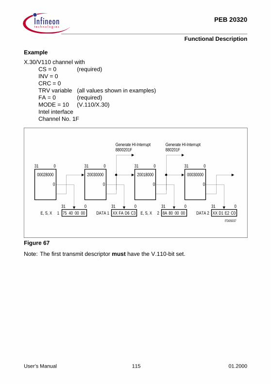
PEB 20320
Functional Description
Example
X.30/V110 channel withCS = 0 (required)INV = 0CRC = 0TRV variable (all values shown in examples)FA = 0 (required)MODE = 10 (V.110/X.30)Intel interfaceChannel No. 1F
Figure 67
Note: The first transmit descriptor must have the V.110-bit set.
ITD05037
00028000
0
75 40 00 00
031
C3D6FAXX
20030000 20018000
8A 80 00 00
31 0
Generate HI-Interrupt8800201F
31 0
31 0
31 0
31 0
031
00030000
031
C0E2D1XX
0 0 0
DATA 2E, S, X 21E, S, X DATA 1
880201FGenerate HI-Interrupt
User’s Manual 115 01.2000

PEB 20320
Functional Description
TRV = 000 0 0 0 0 0 0 01 1 1 1 1 1 1 01 1 1 1 1 1 1 11 1 1 1 1 0 0 01 0 0 0 0 0 0 11 0 1 0 1 1 1 01 0 0 0 0 0 0 01 0 0 0 0 0 0 11 0 0 0 0 0 0 01 0 0 0 0 0 0 1
0 0 0 0 0 0 0 01 0 0 0 0 0 0 01 0 0 1 1 1 1 11 1 1 1 1 1 1 01 1 1 1 1 1 1 11 0 1 0 1 1 1 01 0 0 0 0 0 0 01 0 0 1 1 1 1 11 1 1 1 1 0 0 01 0 0 0 0 0 0 1
0 0 0 0 0 0 0 01 0 0 0 0 0 0 01 0 0 1 1 1 1 11 1 1 1 1 0 0 01 0 0 0 0 0 0 11 0 1 0 1 1 1 01 1 1 1 1 1 1 01 1 1 1 1 1 1 11 1 1 1 1 1 1 01 1 1 1 1 1 1 1
0 0 0 0 0 0 0 01 0 0 0 0 0 0 11 0 0 0 0 0 0 01 0 0 0 0 0 0 11 0 0 0 0 0 0 01 1 0 1 0 0 0 11 0 0 0 0 0 0 11 0 0 0 0 0 0 01 0 0 0 0 0 0 11 0 0 0 0 0 0 0
0 0 0 0 0 0 0 01 0 0 0 0 0 0 11 0 0 1 1 1 1 01 1 1 1 1 0 0 11 0 0 0 0 0 0 01 1 0 1 0 0 0 11 0 0 0 0 0 0 11 0 0 0 0 0 0 01 0 0 0 0 1 1 11 1 1 1 1 1 1 0
0 0 0 0 0 0 0 01 1 1 1 1 1 1 11 1 1 0 0 0 0 01 0 0 0 0 0 0 11 0 0 0 0 0 0 01 1 0 1 0 0 0 11 0 0 0 0 0 0 11 0 0 1 1 1 1 01 1 1 1 1 0 0 11 0 0 0 0 0 0 0
D6 = 11 0 1 0 1 1 0B6B5B4B3B2B1
FA = 11 1 1 1 0 1 0B6B5B4B3B2B1
Change of E-, S-, X-bits
SAX
SB1 E1E2E3E4E5E6E7
User’s Manual 116 01.2000

PEB 20320
Functional Description
TRV = 01
TRV = 10
0 0 0 0 0 0 0 01 1 1 1 1 1 1 01 1 1 0 0 0 0 11 0 0 0 0 0 0 01 0 0 0 0 0 0 11 0 1 0 1 1 1 01 0 0 0 0 1 1 01 1 1 1 1 1 1 11 0 0 0 0 1 1 01 1 1 0 0 0 0 1
0 0 0 0 0 0 0 01 0 0 0 0 1 1 01 1 1 0 0 0 0 11 1 1 1 1 1 1 01 1 1 1 1 1 1 11 0 1 0 1 1 1 01 0 0 0 0 0 0 01 0 0 0 0 0 0 11 0 0 0 0 0 0 01 0 0 0 0 0 0 1
0 0 0 0 0 0 0 01 0 0 0 0 1 1 11 1 1 0 0 0 0 01 0 0 0 0 0 0 11 0 0 1 1 1 1 01 1 0 1 0 0 0 11 1 1 1 1 0 0 11 0 0 0 0 0 0 01 0 0 0 0 1 1 11 1 1 0 0 0 0 0
E2 = 1 1 1 0 0 0 1 0B6B5B4B3B2B1
D1 = 1 1 0 1 0 0 0 1B6B5B4B3B2B1
Change of E-, S-, X-bits
FA (last byte of DATA 1)→ 1 1 1 1 1 0 1 0
B6B5B4B3B2B1
1 1 0 0 0 0 0 0B6B5B4B3B2B1
C0 (first byte of DATA 2) →
SAX
SB1 E1E2E3E4E5E6E7
0 0 0 0 0 0 0 01 1 1 1 1 0 0 01 0 0 0 0 0 0 11 0 0 1 1 1 1 01 0 0 1 1 0 0 11 0 1 0 1 1 1 01 0 0 1 1 0 0 01 1 1 1 1 1 1 11 0 0 0 0 0 0 01 0 0 0 0 0 0 1
0 0 0 0 0 0 0 01 0 0 1 1 0 0 11 0 0 0 0 1 1 01 1 1 0 0 0 0 11 0 0 1 1 0 0 01 1 0 1 0 0 0 11 11 01 11 0
SAX
SB1 E1E2E3E4E5E6E7
E2 = 1 1 1 0 0 0 1 0B6B5B4B3B2B1
D1 = 1 1 0 1 0 0 0 1B6B5B4B3B2B1
Change of E-, S-, X-bits
User’s Manual 117 01.2000

PEB 20320
Functional Description
TRV = 11
For INV = 1 (channel inversion) all bits are inverted. For Motorola mode the data sectionswould have to have the form to yield the same output data.
Figure 68
0 0 0 0 0 0 0 01 1 1 0 0 0 0 01 0 1 1 0 1 0 11 0 1 0 1 1 1 01 0 0 0 0 0 0 11 0 1 0 1 1 1 01 0 1 0 0 0 1 01 1 0 0 0 1 0 11 01 1
Change of E-, S-, X-bits
ITD05038
C3 86 FA XX
031
C0 E2 D1 XX
31 0
DATA 1E, S, X 1
31 0
75400000 E, S, X 2
031
8A800000XX XX 00 03
DATA 2
User’s Manual 118 01.2000

PEB 20320
Functional Description
V.110/X.30
Receive DirectionGeneral Features
In receive direction
– the starting sequence (00H followed by a ‘1’-bit) after initialization ofloss of synchronism is detected.
– the synchronization pattern is monitored, after 3 consecutiveerroneous frames a loss of synchronism is detected.
– a change of E-, S-, X-bits is monitored and reported by an interrupt.– the data bits are extracted and written into the data section.
More detailed description of the individual features:
1. and 2. the receiver can be in one of 2 states:
Figure 69
Data extraction and monitoring of a change of E-, S-, X-bits and synchronization patternis only performed in synchronized state.
In the asynchronous state the receiver waits for the synchronization patter. The ‘1’-bit isthen interpreted as bit 1 of octet 2.
3. During the synchronized state a change of E, S, X-bits from one frame to the next andeven within a frame (for SA, SB bits) is monitored. Only one interrupt per frame isreported even if SA e.g. changes 3 times within the frame. The E-, S-, X-bits reportedin the interrupt are S9 for SB and S8 for SA and the second occurrence of X for X.
4. The bits written into the data section are marked by O in Table 2 to Table 4. Asshown, bits repeated in the serial data are only strobed than at their last instance.
ITD05039
RESET
Unsynchronous State
Synchronous State
3 Consecutive Erroneous Frames(with a Frame Error)by a "1" bit
8 * "0" bit followed
User’s Manual 119 01.2000
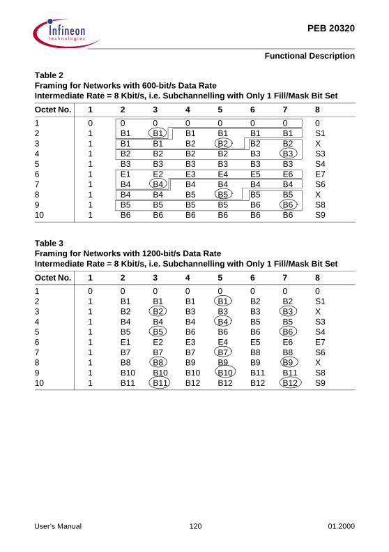
PEB 20320
Functional Description
Table 2Framing for Networks with 600-bit/s Data RateIntermediate Rate = 8 Kbit/s, i.e. Subchannelling with Only 1 Fill/Mask Bit Set
Octet No. 1 2 3 4 5 6 7 8
12345678910
0 0 0 0 0 0 0 01 B1 B1 B1 B1 B1 B1 S11 B1 B1 B2 B2 B2 B2 X1 B2 B2 B2 B2 B3 B3 S31 B3 B3 B3 B3 B3 B3 S41 E1 E2 E3 E4 E5 E6 E71 B4 B4 B4 B4 B4 B4 S61 B4 B4 B5 B5 B5 B5 X1 B5 B5 B5 B5 B6 B6 S81 B6 B6 B6 B6 B6 B6 S9
Table 3Framing for Networks with 1200-bit/s Data RateIntermediate Rate = 8 Kbit/s, i.e. Subchannelling with Only 1 Fill/Mask Bit Set
Octet No. 1 2 3 4 5 6 7 8
12345678910
0 0 0 0 0 0 0 01 B1 B1 B1 B1 B2 B2 S11 B2 B2 B3 B3 B3 B3 X1 B4 B4 B4 B4 B5 B5 S31 B5 B5 B6 B6 B6 B6 S41 E1 E2 E3 E4 E5 E6 E71 B7 B7 B7 B7 B8 B8 S61 B8 B8 B9 B9 B9 B9 X1 B10 B10 B10 B10 B11 B11 S81 B11 B11 B12 B12 B12 B12 S9
User’s Manual 120 01.2000

PEB 20320
Functional Description
They are grouped together in the form:
31 0
1 1 B6 B5 B4 B3 B2 B1 1 1 B12 B11 B10 B9 B8 B7 1 1 B18 B17 B16 B15 B14 B13 1 1 B24 B23 B22 B21 B20 B19
(for Motorola mode)
31 0
1 1 B24 B23 B22 B21 B20 B19 1 1 B18 B17 B16 B15 B14 B13 1 1 B12 B11 B10 B9 B8 B7 1 1 B6 B5 B4 B3 B2 B1
(for Intel mode)
where for the 600 bit/s e.g. B1 to B6 belong to the first 10-octet frame, B7 to B12 belongto the second 10-octet frame etc.
Table 4Framing for Networks with 2400-bit/s Data RateIntermediate Rate = 8 Kbit/s, i.e. Subchannelling with Only 1 Fill/Mask Bit Set
Octet No. 1 2 3 4 5 6 7 8
123456789
10
0 0 0 0 0 0 0 01 B1 B1 B2 B2 B3 B3 S11 B4 B4 B5 B5 B6 B6 X1 B7 B7 B8 B8 B9 B9 S31 B10 B10 B11 B11 B12 B12 S41 E1 E2 E3 E4 E5 E6 E71 B13 B13 B14 B14 B15 B15 S61 B16 B16 B17 B17 B18 B18 X1 B19 B19 B20 B20 B21 B21 S81 B22 B22 B23 B23 B24 B24 S9
Table 5Framing for Networks with 4800-, 9600-, 19200-, 38400-bit/s Data RateIntermediate Rate = 8, 16, 32, 64 Kbit/s, i.e. Subchannelling with 1, 2, 4, 8 Fill/Mask Bit Set
Octet No. 1 2 3 4 5 6 7 8
123456789
10
0 0 0 0 0 0 0 01 B1 B2 B3 B4 B5 B6 S11 B7 B8 B9 B10 B11 B12 X1 B13 B14 B15 B16 B17 B18 S31 B19 B20 B21 B22 B23 B24 S41 E1 E2 E3 E4 E5 E6 E71 B25 B25 B27 B29 B29 B30 S61 B31 B32 B33 B35 B35 B36 X1 B37 B36 B39 B41 B41 B42 S81 B43 B44 B45 B47 B47 B48 S9
User’s Manual 121 01.2000

PEB 20320
Functional Description
Options
The different options for this mode are the framing pattern as shown in Table 2 toTable 5 is programmed by the bits TRV.
Interrupts
The possible interrupts for this mode are
FRC: issued if the receiver has detected a change of S-, X-, E-bits; the value of the bitsE7, …, E1, S8 for SA and S9 for SB and the second occurrence of X within the 10-octet frame is reported within the same interrupt.(maskable by CH in the channel specification
HI: issued if the HI bit is detected in the transmit descriptor (not maskable).
ERR: issued if one of the following receive errors has occurred:– a fast receive abort channel command was issued (this leads to a setting of the
RA bit in the status byte)– data could only partly be stored due to internal buffer overflow of RB– 3 consecutive frames had an error in the synchronization
pattern (loss of synchronism)– the HOLD bit in the receive descriptor was detected (this leads to a setting of the
RA bit in status in the receive descriptor). (maskable by RE in the channel specification)
FO: issued if due to inaccessibility of the internal buffer (RB) one or more changes ofE-, S-, X-bits and/or loss of synchronism information have been lost.(maskable by RE in the channel specification)
Example
V.110/X.30 channel withCS = 0 (required)INV = 0CRC = 0TRV = 00 (600 bit/s)FA = 0MODE = 10 (V.110/X.30)Motorola interfaceChannel No. D
User’s Manual 122 01.2000

PEB 20320
Functional Description
Figure 70a
ITS08219
0 0 0 0 0000
0 0 0 0. ..
0 0 0 000011 0 0 001 1 1
MUNICH32 waits for synchronization after reset
11 01 1 1 10 0 111 01 1 0 E9 HB3B4B6 B2 B1B50 111 01 10
011 1111 1
11 1 1
11 100 11 1
11 0011 1 1
0 01 1110 0
11 00
Reported as XReported as SAReported as SB
0 000 1
100111 1
0 01 1
1 001
11 111 1 1
11 1 00 01 0
0 1111 01 1111001
1 0 0 0 0000 0 00000 1
Error in synchronization pattern
B5 B1B2B6 B4 B3HCA010 01 1 10
No change of E, S, X Bits
11 1
0000
00000
0 0 00
No change of E, S, X Bits
111 00 0 D2HB3B4B6 B2 B1B5
Error in synchronization pattern
111 1
0 01 1
11 1 1
1 1 01
1111
1 0 0 0 0000 0 0 00000
11 1 111 1 111 1 111 1111 1 111 1 111 1 111 1 111
1 1110 0
0001
011
1 1
1111 1 11 1
1 0
Reported as SA
01B5 B1B2B6 B4 B3
HFA01 1 11 1
Change of E, S, X Bits; but SA is still reported as ’1’0
1
11 1
11 1
0
Error in synchronization pattern
00
0 001
111
1111
0 0 0 0 00000 000
000 00 000
000 0 0000
000 00 00 00
0 00 00 00 0 0
User’s Manual 123 01.2000

PEB 20320
Functional Description
Figure 70b
ITS08220
Error in synchronization pattern
1 0 0 00 0 0 00000
1
0 011 111 11 0 0 0 000 1
10 0 00001
111 11 01 0 0 0 000 1
1 1 111
1111 1 11 11111 1 11 11111 1 11 11111 1 11 11111 1 11 11111 1 11 11111 1 11 11111 1 11 11111 1 11 1
0 0 0 0 00000 0 00001
1 1 1 1
EDH11 1011 1
111 1
11 00
11 1 1
11 111 1 1 1
Error in synchronization pattern
No change of E, S, X Bits
Change of E, S, X Bits
HFF
1 111 11 100011 11 100011 11 100011 11 100011 11 100011 11 100011 11 100011 11 10001
0 0 0 0 00000 0 0 000000 0 0 000000 0 0 000000 0 0 000000 0 0 000000 0 0 000000 0 0 000000 0 0 000000 0 0 00000
FFH
HC0
No error in synchronization pattern
Change of E, S, X Bits
Change of E, S, X Bits
User’s Manual 124 01.2000

PEB 20320
Functional Description
Figure 71
For Intel mode the data sections have the form:
Figure 72
ITD05040
00080000
E9 CA FA D2
031
C0FFFFED
20040000
31 0
8800202D
31 0
31 0
8800022D
st1 Desc 2 Descnd
Loss of Synch.
8E5B002D8E5B002D
8C00002D8F57002D8FFF002D
40042000 40040000
ITD05041
C0 FF FF ED
031
ndof 1 Descst
31 0
E9CAFAD2
of 2 Desc
User’s Manual 125 01.2000

PEB 20320
Functional Description
2.5 Boundary Scan Unit
In MUNICH32 a Test Access Port (TAP) controller is implemented. The essential part ofthe TAP is a finite state machine (16 states) controlling the different operational modesof the boundary scan. Both, TAP controller and boundary scan, meet the requirementsgiven by the JTAG standard: IEEE Std. 1149.1. Figure 73 gives an overview.
Figure 73Block Diagram of Test Access Port and Boundary Scan
Test handling is performed via the pins JTEST0 (TCK), JTEST1 (TMS), JTEST2 (TDI)and JTEST3 (TDO). Test data at JTEST2 (TDI) are loaded with a 4-MHz clock signalconnected to JTEST0 (TCK). ‘1’ or ‘0’ on JTEST1 (TMS) causes a transition from onecontroller state to an other; constant ‘1’ on JTEST1 (TMS) leads to normal operation ofthe chip.
If no boundary scan testing is planned JTEST1 (TMS) and JTEST2 (TDI) do not need tobe connected since pull-up transistors ensure high input levels in this case. Neverthelessit would be a good practice to put the unused inputs to defined levels. In this case, if theJTAG is not used:JTEST1 = JTEST0 = ‘1’.
After switching on the device (VDD = 0 to 5 V) a power-on reset is generated which forcesthe TAP controller into test logic reset state.
ClockGeneration
CLOCK
ResetPower ON
Reset
TAP Controller
-Finite State Machine-Instruction Register (3 bits)-Test Signal Generator
JTEST0 (TCK)
JTEST1 (TMS)
JTEST2 (TDI)
JTEST3 (TDO)
CLOCK
TestControl
Data IN
Control Bus
6
ID Data OUT
SS Data OUT
BS Data IN
Iden
tifica
tion
Scan
(32
Bits
)
Boun
dary
Sca
n (n
Bits
)
12
n
Pins
ITB03509
Enable
Data OUT
Test Access Port
User’s Manual 126 01.2000

PEB 20320
Functional Description
Table 6Boundary Scan Sequence in PEB 20320
JTEST2 (TDI) →
Pin No.
Pin I/O Number ofBoundary Scan Cells
Constant Value
1234567891011121314151617181920212223242526272829303132333435
ResetSCLKTESTARTDATATSPTCLKI/MB16Ready/DSACKBERRHLDA/BGHLDAO/BGOBGACKHOLD/BRADS/ASDSWR/RWBE3BE2D0BE1D1BE0D2A2D3A3D4A4D5A5D6A6D7
IIIIOIIIIIIIOI/OI/OOOOOOI/OOI/OOI/OOI/OOI/OOI/OOI/OOI/O
11112111111123322222323232323232323
011000000000000001010000100000110000000000000000000000000000000000000
User’s Manual 127 01.2000

PEB 20320
Functional Description
Table 6Boundary Scan Sequence in PEB 20320 (cont’d)
JTEST2 (TDI) →
Pin I/O Number ofBoundary Scan Cells
Constant Value
3637383940414243444546474849505152535455565758596061626364656667686970
A7D8A8D9A9D10A10D11A11D12A12D13A13D14A14D15A15D16A16D17A17D18A18D19A19D20A20D21A21D22A22D23A23D24A24
OI/OOI/OOI/OOI/OOI/OOI/OOI/OOI/OOI/OOI/OOI/OOI/OOI/OOI/OOI/OOI/OOI/OO
23232323232323232323232323232323232
000000000000000000000000000000000000000000000000000000000000000000000000000000000000000
User’s Manual 128 01.2000
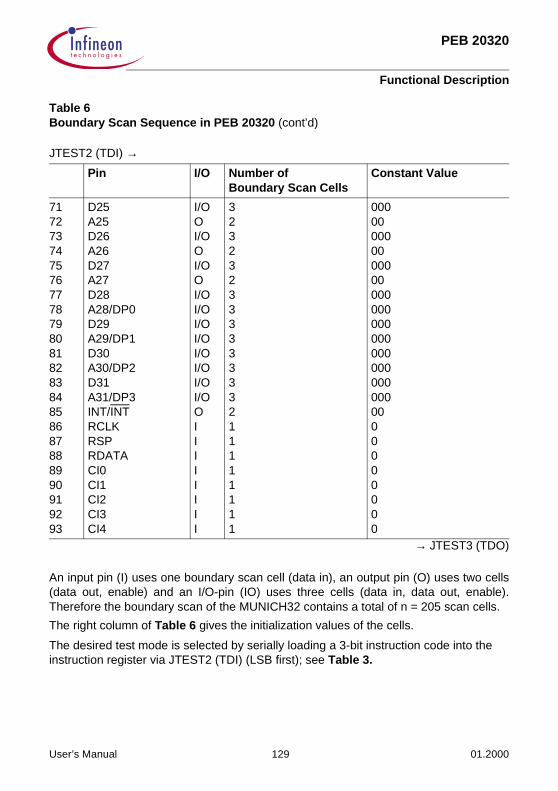
PEB 20320
Functional Description
→ JTEST3 (TDO)
An input pin (I) uses one boundary scan cell (data in), an output pin (O) uses two cells(data out, enable) and an I/O-pin (IO) uses three cells (data in, data out, enable).Therefore the boundary scan of the MUNICH32 contains a total of n = 205 scan cells.
The right column of Table 6 gives the initialization values of the cells.
The desired test mode is selected by serially loading a 3-bit instruction code into the instruction register via JTEST2 (TDI) (LSB first); see Table 3.
Table 6Boundary Scan Sequence in PEB 20320 (cont’d)
JTEST2 (TDI) →
Pin I/O Number ofBoundary Scan Cells
Constant Value
7172737475767778798081828384858687888990919293
D25A25D26A26D27A27D28A28/DP0D29A29/DP1D30A30/DP2D31A31/DP3INT/INTRCLKRSPRDATACI0CI1CI2CI3CI4
I/OOI/OOI/OOI/OI/OI/OI/OI/OI/OI/OI/OOIIIIIIII
32323233333333211111111
0000000000000000000000000000000000000000000000000
User’s Manual 129 01.2000
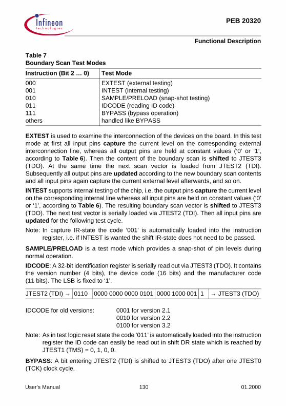
PEB 20320
Functional Description
EXTEST is used to examine the interconnection of the devices on the board. In this testmode at first all input pins capture the current level on the corresponding externalinterconnection line, whereas all output pins are held at constant values (‘0’ or ‘1’,according to Table 6). Then the content of the boundary scan is shifted to JTEST3(TDO). At the same time the next scan vector is loaded from JTEST2 (TDI).Subsequently all output pins are updated according to the new boundary scan contentsand all input pins again capture the current external level afterwards, and so on.
INTEST supports internal testing of the chip, i.e. the output pins capture the current levelon the corresponding internal line whereas all input pins are held on constant values (‘0’or ‘1’, according to Table 6). The resulting boundary scan vector is shifted to JTEST3(TDO). The next test vector is serially loaded via JTEST2 (TDI). Then all input pins areupdated for the following test cycle.
Note: In capture IR-state the code ‘001’ is automatically loaded into the instructionregister, i.e. if INTEST is wanted the shift IR-state does not need to be passed.
SAMPLE/PRELOAD is a test mode which provides a snap-shot of pin levels duringnormal operation.
IDCODE: A 32-bit identification register is serially read out via JTEST3 (TDO). It containsthe version number (4 bits), the device code (16 bits) and the manufacturer code(11 bits). The LSB is fixed to ‘1’.
IDCODE for old versions: 0001 for version 2.10010 for version 2.20100 for version 3.2
Note: As in test logic reset state the code ‘011’ is automatically loaded into the instructionregister the ID code can easily be read out in shift DR state which is reached byJTEST1 (TMS) = 0, 1, 0, 0.
BYPASS: A bit entering JTEST2 (TDI) is shifted to JTEST3 (TDO) after one JTEST0(TCK) clock cycle.
Table 7Boundary Scan Test Modes
Instruction (Bit 2 … 0) Test Mode
000001010011111others
EXTEST (external testing)INTEST (internal testing)SAMPLE/PRELOAD (snap-shot testing)IDCODE (reading ID code)BYPASS (bypass operation)handled like BYPASS
JTEST2 (TDI) → 0110 0000 0000 0000 0101 0000 1000 001 1 → JTEST3 (TDO)
User’s Manual 130 01.2000

PEB 20320
Operational Description
3 Operational Description
3.1 Reset State
Upon reset MUNICH32 is set to its initial state. The active high system reset clears theinternal logic and causes MUNICH32 to tristate all output lines. Channel processing isdeactivated. After reset all buffers are empty and no buffer size of TB is allocated to thechannels. The DMA controller state is set to the hold condition for all link lists. Thedescriptor and data pointers remain at a random value.
The bits RO and TO are set to ‘1’ and RA and TA are set to ‘0’ for all logical channels byreset. All time slots are connected to the logical channel 0 and the following configurationis set:
Action Specification
LOC = LOOP = LOOPI = 0
PCM = T1/DS1 × 24-channel 1.536 Mbit/s (000)
MFL = 0
Time Slot Assignment
fill/mask = 00H, i.e. all bits masked/set to ‘1’
RTI, TTI = 0
channel number = 00H
Channel Specification
MODE = 00, i.e. TMA
FA = 0
IFTF = 0
CRC = 0
INV = 0
TRV = 00,
RA = 0
TA = 0
TH = 0
RO = 1
TO = 1
User’s Manual 131 01.2000

PEB 20320
Operational Description
Transmit Descriptor
FNUM = 00H, i.e. shared flags in HDLC, only eight zero bits between sent frames forTMB.
The E-, S-, X-bits are all set to zero internally by the reset. The receiver is set into theITF/IDLE state for all channels, i.e. it assumes that on the line there are ‘1’s as interframetime-fill for HDLC.
3.2 Initialization Procedure
After reset MUNICH32 remains in the initial state until the microprocessor generates anaction request. In the action specification the initialization sequence is defined. Thesequence can be split up into individual procedures of each channel or in one singleprocedure to initialize all channels at the same time. For all procedures the time slotassignment and the selected channel specifications are loaded into the CSR-RAM. Toprevent malfunction the initialization of the link lists and the allocation of the buffer sizeto the channels has to be specified before the transmission can be started. The interruptqueue must be established as well. MUNICH32 assumes that time slot 0 starts on thereceive and transmit lines. They can be resynchronized by 2 rising edges of TSP andRSP respectively. The first rising edge of TSP/RSP should not take place within the first1000 SCLK clock cycles after deassertion of the reset pin.
Before this resynchronization the host should neither remove RO = 1, TO = 1 nor setLOOP or LOOPI to ‘1’ for any logical channel. During this time any incoming data isignored, the transmit data line tristated.
For each action service the device first reads the control start address in the control andconfiguration section which is located under a fixed address determined by the inputsignals (CI(4:0)).
The values of CI(4:0) can be changed during operation. The values are used after thenext falling edge of AR.
CI4 is the polarity of A31 … A22
CI3 is the polarity of A21 … A16
CI2 is the polarity of A15 … A4
CI1 is the polarity of A3
CI0 is the polarity of A2
A0, A1 = 0
for example CI(4:0) = 10101
ADDRESS = 1111.1111.1100.0000.1111.1111.1111.0100
User’s Manual 132 01.2000

PEB 20320
Operational Description
Figure 74
Figure 75CI-Pin Decoding
31 30 29 28 27 26 25 24 23 22 21 20 19 18 17 16 15 14 13 12 11 10 9 8 7 6 5 4 3 2 1 0
CI4 CI3 CI2 CI1 CI0 0 0
CI4 CI3 CI2 CI1 CI0 Loc. of Ctrl. Start Addr.
CI4 CI3 CI2 CI1 CI0 Loc. of Ctrl. Start Addr.
0 0 0 0 0 0000 0000 1 0 0 0 0 FFC0 0000
0 0 0 0 1 0000 0004 1 0 0 0 1 FFC0 0004
0 0 0 1 0 0000 0008 1 0 0 1 0 FFC0 0008
0 0 0 1 1 0000 000C 1 0 0 1 1 FFC0 000C
0 0 1 0 0 0000 FFF0 1 0 1 0 0 FFC0 FFF0
0 0 1 0 1 0000 FFF4 1 0 1 0 1 FFC0 FFF4
0 0 1 1 0 0000 FFF8 1 0 1 1 0 FFC0 FFF8
0 0 1 1 1 0000 FFFC 1 0 1 1 1 FFC0 FFFC
0 1 0 0 0 003F 0000 1 1 0 0 0 FFFF 0000
0 1 0 0 1 003F 0004 1 1 0 0 1 FFFF 0004
0 1 0 1 0 003F 0008 1 1 0 1 0 FFFF 0008
0 1 0 1 1 003F 000C 1 1 0 1 1 FFFF 000C
0 1 1 0 0 003F FFF0 1 1 1 0 0 FFFF FFF0
0 1 1 0 1 003F FFF4 1 1 1 0 1 FFFF FFF4
0 1 1 1 0 003F FFF8 1 1 1 1 0 FFFF FFF8
0 1 1 1 1 003F FFFC 1 1 1 1 1 FFFF FFFC
User’s Manual 133 01.2000

PEB 20320
Detailed Register Description
4 Detailed Register Description
4.1 Organization of the Shared Memory
Because the MUNICH32 reads only long words, all addresses of the link lists, interruptqueue and the CCS must be a multiple of four; i.e. the two least significant bits of theaddress must be ‘00’. Figure 76 depicts the organization of the shared memory for oneMUNICH32.
User’s Manual 134 01.2000
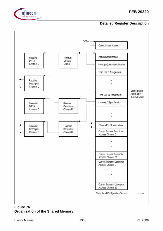
PEB 20320
Detailed Register Description
Figure 76Organization of the Shared Memory
ReceiveDATAChannel 0
InterruptCircularQueue
Control Start Address
Action Specification
Interrupt Queue Specification
Time Slot 0 Assignment
Channel 0 Specification
Time Slot 31 Assignment
Channel 31 Specification
Control and Configuration Section
Current Transmit DescriptorAddress Channel 31
Address Channel 0Current Transmit Descriptor
Current Receive DescriptorAddress Channel 31
Current Receive DescriptorAddress Channel 0
CCBA
Last 8 Blocksnot used inT1/DS1 Mode
Channel 0DescriptorReceive
Channel 0DATATransmit
Channel 0DescriptorTransmit Transmit
DescriptorChannel 0
ReceiveDescriptorChannel 0
ITD03508
User’s Manual 135 01.2000

PEB 20320
Detailed Register Description
4.2 Control and Configuration Section
4.2.1 Action Specification (Read Once After Each Action Request Pulse)
All actions are selected by setting the corresponding bits to ‘1’.
PCM: These three bits determine the PCM highway format.
000: T1/DS1 24-channel 1.536 Mbit/s100: T1/DS1 24-channel 1.544 Mbit/s101: CEPT 32-channel110: 4.096-Mbit/s PCM format and even numbered time slots111: 4.096-Mbit/s PCM format and odd numbered time slots
MFL: Maximum Frame Length (up to 8191 bytes); MUNICH32 monitors the frame lengthof the incoming HDLC, TMB or TMR frames. If the maximum frame length isexceeded an interrupt is generated and the current frame aborted. The lengthcheck is active in all modes except transparent mode A and V.110/X.30. Thereforein all other modes one has to write a reasonable value to MFL after reset. MFL isthe same for all logical channels.
Table 8Buffer Size of the Control and Configuration Section
Control and Configuration Section Number of Long Words
Action specification 1
Interrupt queue specification 2
Time slot assignment 32
Channel specification 128
Current descriptor address 64
31 30 29 28 27 26 25 24 23 22 21 20 19 18 17 16
PCM
15 14 13 12 11 10 9 8 7 6 5 4 3 2 1 0
IN IC0 0 Channel Number IM RES LOC LOOP LOOPI IA 0 0
MFL
User’s Manual 136 01.2000
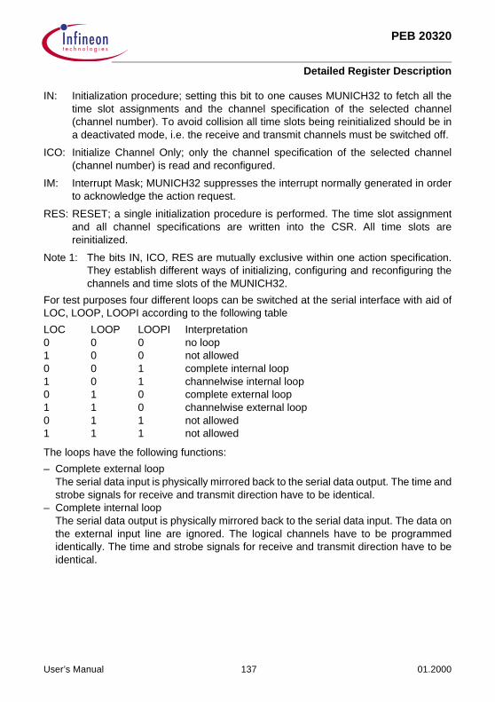
PEB 20320
Detailed Register Description
IN: Initialization procedure; setting this bit to one causes MUNICH32 to fetch all thetime slot assignments and the channel specification of the selected channel(channel number). To avoid collision all time slots being reinitialized should be ina deactivated mode, i.e. the receive and transmit channels must be switched off.
ICO: Initialize Channel Only; only the channel specification of the selected channel(channel number) is read and reconfigured.
IM: Interrupt Mask; MUNICH32 suppresses the interrupt normally generated in orderto acknowledge the action request.
RES: RESET; a single initialization procedure is performed. The time slot assignmentand all channel specifications are written into the CSR. All time slots arereinitialized.
Note 1: The bits IN, ICO, RES are mutually exclusive within one action specification.They establish different ways of initializing, configuring and reconfiguring thechannels and time slots of the MUNICH32.
For test purposes four different loops can be switched at the serial interface with aid ofLOC, LOOP, LOOPI according to the following table
LOC LOOP LOOPI Interpretation0 0 0 no loop1 0 0 not allowed0 0 1 complete internal loop1 0 1 channelwise internal loop0 1 0 complete external loop1 1 0 channelwise external loop0 1 1 not allowed1 1 1 not allowed
The loops have the following functions:
– Complete external loopThe serial data input is physically mirrored back to the serial data output. The time andstrobe signals for receive and transmit direction have to be identical.
– Complete internal loopThe serial data output is physically mirrored back to the serial data input. The data onthe external input line are ignored. The logical channels have to be programmedidentically. The time and strobe signals for receive and transmit direction have to beidentical.
User’s Manual 137 01.2000

PEB 20320
Detailed Register Description
– Channelwise external loopOne single logical channel is mirrored logically from serial data input to serial dataoutput. The other channels are not affected by this operation. The data rate for thissingle logical channel has to be identical for receive and transmit direction.
– Channelwise internal loopOne single logical channel is mirrored logically from serial data output to serial datainput. The other channels are not affected by this operation. The data rate for thissingle logical channel has to be the same for receive and transmit direction.
See Chapter 5.1 and Chapter 5.3.2 for a more detailed discussion of test loops.
All loops of the MUNICH32 V3.2 are under complete software control. Loops can beclosed and opened via software.
Handling of the MUNICH32 V3.2 loops:
Switch loops on:
RES = IN = ICO = ‘0’LOC, LOOP, LOOPI for selected loop typePCM, MFL, IM, IA don’t change the previous valuesCHANNEL NUMBER in case of channelwise loops use the selected
channel numberin case of complete loops use channel number of anactive channel.
Switch loops off:
RES = IN = ICO = ‘0’LOC = ‘0’, LOOP = LOOPI = ‘1’PCM, MFL, IM, IA don’t change the previous valuesCHANNEL NUMBER use channel number used with the ‘switch loop on’.
IA: Interrupt Attention; a new interrupt queue is defined by the host. MUNICH32 readsthe interrupt queue specification and writes the interrupt information into the newinterrupt queue.
User’s Manual 138 01.2000

PEB 20320
Detailed Register Description
Figure 77Action Specification
ITS08221
31 30 29 28 27 26 25 24 23 22 21 20 19 18 17 16 15 14 13 12 11 10 9 8 7 6 5
PCM
IN ICO
LOCChannel
Number0
4 3 2 1 0
0 0
RES
IM LOO
PLO
OPI
IA
MFL
Maximum Frame Length
Maximum size of a received framein HDLC, TMB and TMR mode (up to 8192 bytes).A received frame is aborted and an interruptis generated if the size of a received frameexceeds the MFL value.MFL applies to all channels.
PCM Highway Format
0 0 00 0 10 1 00 1 11 0 01 0 11 1 01 1 1
Not AllowedT1/DS1 24 Time-Slots, 1.536 Mbit/s
Channel No.
Used inconjunctionwith IN
Initialize Channel Only
Only the channel spec.
(channel number) isread and reconfigured.
Initialization Procedure
Read the complete time-slotassignment and the channel
spec. of the specified channel(channel number).
Interrupt Attention
A new interrupt queuehas been defined. Readthe interrupt queuespecification.
No LoopComplete Internal Loop
Channelwise int. LoopChannelwise ext. Loop
1 1 11 1 01 0 11 0 00 1 10 1 00 0 10 0 0
Loops
Complete Internal Loop
Read the complete time-slot assignmentRead all channel specificationsReinitialize all time-slots
Reset
Do not generate the ARACK & ARF interrupt
Interrupt Mask
and ICO
of the selected channel
Not AllowedNot Allowed
CEPT 32 Time-Slots, 2.048 Mbit/s4.096 Mbit/s PCM Format, even Time-Slots4.096 Mbit/s PCM Format, odd Time-Slots
Not Allowed
Not AllowedNot Allowed
T1/DS1 24 Time-Slots, 1.544 Mbit/s
User’s Manual 139 01.2000

PEB 20320
Detailed Register Description
4.2.2 Interrupt Queue Specification
The interrupt queue is specified as a kind of block (queue), starting on a start address(programmable) with a defined length (programmable). Both, the start address and thequeue length are programmable in the Interrupt Queue Specification of the Control andConfiguration Section.
Figure 78
The minimum queue size is 16 long words; the maximum queue size is 4096 long words.
For each interrupt arising, the MUNICH32 writes the interrupt information into theinterrupt queue, will increment the pointer to the next address in this block automaticallyand will generate an interrupt pulse at each interrupt occasion. It is up to the processorto read the interrupt informations out of the interrupt queue. If the MUNICH32 arrives atthe end of the interrupt queue, it will jump to the start address of the interrupt block again(cyclic queue) and completely overwrite the previous information.
Therefore the length of the interrupt queue should be calculated so, that the MUNICH32will not overwrite information which was not yet read by the processor.
31 30 29 28 27 26 25 24 23 22 21 20 19 18 17 16
Interrupt Queue Address
0 0 0 0 0 0 0 0 0 0 0 0 0 0 0 0
15 14 13 12 11 10 9 8 7 6 5 4 3 2 1 0
Interrupt Queue Address
0 0 0 0 0 0 0 0 n
START ADDRESS(Interrupt QueueAddress)
length =(n + 1) × 16 long wordswhere 0 ≤ n ≤ 255
overwrite
.
.
.
interrupt information long word 1
interrupt information long word 2
interrupt information long word 3
interrupt information long word (n+1)x16
User’s Manual 140 01.2000

PEB 20320
Detailed Register Description
4.2.3 Interrupt Information
The next table shows the bit assignments for the interrupt information long word.
When an interrupt occurs MUNICH32 sets the INT bit and writes the interrupt informationand the channel number into the interrupt circular buffer. At the same time it generatesan interrupt pulse. The classes of error (for example host initiated interrupt or CRC error)of a channel in one direction are treated independently of each other. If several interruptevents coincide they will be indicated to the host with one shared interrupt.
Bit assignment for interrupt queue
There are 3 classes of bits in the interrupt:
1. Bits present in each interrupt:INT: this bit is always set to ‘1’VN(3:1): these bits are ‘000’ for version 1.1
‘001’ for version 2.1‘010’ for version 2.2‘100’ for version 3.2‘110’ for version 3.4
31 30 29 28 27 26 25 24 23 22 21 20 19 18 17 16
INT 0 Interrupt Information
15 14 13 12 11 10 9 8 7 6 5 4 3 2 1 0
Interrupt Information Channel Number/Direction
31 30 29 28 27 26 25 24 23 22 21 20 19 18 17 16
INT 0 VN3 VN2 VN1 FRC E7 E6 E5 E4 E3 E2 E1 SB SA X
15 14 13 12 11 10 9 8 7 6 5 4 3 2 1 0
ARACK ARF HI FI IFC SF ERR FO 0 0 RT Channel Number
User’s Manual 141 01.2000
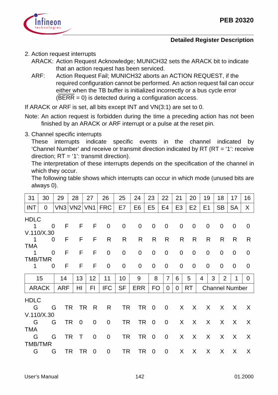
PEB 20320
Detailed Register Description
2. Action request interruptsARACK: Action Request Acknowledge; MUNICH32 sets the ARACK bit to indicate
that an action request has been serviced.ARF: Action Request Fail; MUNICH32 aborts an ACTION REQUEST, if the
required configuration cannot be performed. An action request fail can occureither when the TB buffer is initialized incorrectly or a bus cycle error(BERR = 0) is detected during a configuration access.
If ARACK or ARF is set, all bits except INT and VN(3:1) are set to 0.
Note: An action request is forbidden during the time a preceding action has not beenfinished by an ARACK or ARF interrupt or a pulse at the reset pin.
3. Channel specific interruptsThese interrupts indicate specific events in the channel indicated by‘Channel Number’ and receive or transmit direction indicated by RT (RT = ‘1’: receivedirection; RT = ‘1’: transmit direction).The interpretation of these interrupts depends on the specification of the channel inwhich they occur.The following table shows which interrupts can occur in which mode (unused bits arealways 0).
HDLC1 0 F F F 0 0 0 0 0 0 0 0 0 0 0
V.110/X.301 0 F F F R R R R R R R R R R R
TMA1 0 F F F 0 0 0 0 0 0 0 0 0 0 0
TMB/TMR1 0 F F F 0 0 0 0 0 0 0 0 0 0 0
HDLCG G TR TR R R TR TR 0 0 X X X X X X
V.110/X.30G G TR 0 0 0 TR TR 0 0 X X X X X X
TMAG G TR T 0 0 TR TR 0 0 X X X X X X
TMB/TMRG G TR TR 0 0 TR TR 0 0 X X X X X X
31 30 29 28 27 26 25 24 23 22 21 20 19 18 17 16
INT 0 VN3 VN2 VN1 FRC E7 E6 E5 E4 E3 E2 E1 SB SA X
15 14 13 12 11 10 9 8 7 6 5 4 3 2 1 0
ARACK ARF HI FI IFC SF ERR FO 0 0 RT Channel Number
User’s Manual 142 01.2000

PEB 20320
Detailed Register Description
Where ‘1’ means that the bit is always ‘1’ for this mode‘0’ means that the bit is always ‘0’ for this mode‘F’ means the bit is fixed by the version number‘R’ means a bit that can only be set in the receive direction, i.e. may only
be ‘1’ if RT is ‘1’‘T’ means a bit that can only occur in transmit direction, i.e. may only
be ‘1’ if RT is ‘0’‘TR’ means a bit that can occur in receive or transmit direction‘G’ means a bit of an activation request interrupt which cannot be
‘G’ in a channel specific interrupt‘X’ means a bit fixed by the channel and direction (receive, transmit)
of the event it belongs to.
The meaning of the interrupt bits depend on the mode. We therefore will discuss thembit for bit and indicate the different meanings in the different modes.
FRC: (V.110/X.30 mode, receive direction only)Change of the framing (E, S, X) bits of the V.110/X.30 frame detected.This interrupt is generated whenever a change in the E-, S-, X-bits isdetected, but at most one time within one frame of 10 octets, even if thereis more than one change within the frame. After detecting a receive abortchannel command for one 10-octet frame FRC is also issued.
Ex, Sx, X: (V.110/X.30 mode, receive direction only, only in conjunction with FRC)The value of the bits Ex, Sx, X in the received V.110/X.30 frame. If avalue changes, e.g. 2 times within the same frame only the final changeis reported.If the change was caused by a receive abort channel command all bitsare 0.
HI: (all modes, all direction)Host initiated Interrupt; this bit is set when the MUNICH32 detects theHI bit in the receive or transmit descriptor and branches to the nextdescriptor, or starts polling the hold bit if set.
FI: 1.1 HDLC, TMB, TMR Receive Direction:FI = 1 indicates, that a frame has been received completely or wasstopped by a receive abort channel command or fast receive abort or aHOLD in a receive descriptor. It is set when the MUNICH32 branchesfrom the last descriptor belonging to the frame to the first descriptor of anew frame. It is also set when the descriptor in which the frame finishedcontained a hold bit, the interrupt is then issued when the MUNICH32starts polling the hold bit.
1.2 HDLC, TMB, TMR, TMA Transmit Direction:issued if the FE bit is detected in the transmit descriptor. It is set whenthe MUNICH32 branches to the next transmit descriptor, belonging to a
User’s Manual 143 01.2000

PEB 20320
Detailed Register Description
new frame, or when it starts polling the hold bit if set in conjunction withthe FE bit; ERR and FI are set if a transmit descriptor contains aHOLD bit no FE bit
IFC: (HDLC mode, receive direction only)Idle/Flag Change; an interrupt is generated in HDLC if the devicechanges the interframe time-fill (ITF) state. After reset the device is in theITF idle state. It changes to the ITF flag state if it receives 2 consecutiveflags with or without shared zeroes. It changes back to the ITF idle stateupon reception of 15 contiguous ‘1’-bits or when a receive abort channelcommand is active during 15 received bits.
SF: (HDLC mode, receive direction only, always in conjunction with FI) Short frame detectedA frame with ≤ 16 bits between start flag and end flag or end abort flag
for CRC16≤ 32 bits between start flag and end flag or end abort flag for CRC32
has been detected. The sequences 7E 7FH and 7E FEH and 7E FFH arealso short frames.SF is always in conjunction with ERR except for the frames7E00 007EH for CRC167E00 0000 007EH for CRC32
ERR: always in conjunction with FI = 11.1 HDLC mode Receive Direction
One of the following receive errors occurred– FCS of the frame was incorrect– the bit length of the frame was not divisible by 8– the byte length exceeded MFL– the frame was stopped by 7FH– the frame could only be partly stored due to internal buffer overflow of RB– the frame was ended by a receive abort channel command– the frame could not be transferred to the shared memory completely
because of a hold bit set in a receive descriptor not providing enoughbytes for the frame.
– the frame was aborted by a fast receive abort channel commandA more detailed error analysis can be done by the status information inthe receive descriptor.
1.2 HDLC mode Transmit Directionone of the following transmit errors occurred:– the last descriptor had HOLD = 1 and FE = 0– the last descriptor had NO = 0 and FE = 0
User’s Manual 144 01.2000

PEB 20320
Detailed Register Description
2.1 V.110/X.30 mode Receive Directionone of the following receive errors occurred:– data could only partly stored due to internal buffer overflow of RB– 3 consecutive frames had an error in the synchronization pattern
(loss of synchronism)– a fast receive abort channel command was issued– the data could not be transferred to the shared memory completely
because of a hold bit set in a receive descriptor not providing enoughbytes for the data
– a receive abort channel command was active for at least3 consecutive frames
A more detailed error analysis can be done by the status information inthe receive descriptor.
2.2 V.110/X.30 mode Transmit Directionone of the following transmit errors occurred– the last descriptor had a HOLD = 1 or FE = 1– the last descriptor had FE = 0 and NO = 0
3.1 TMA mode Receive Directionone of the following errors occurred– the data could not be transferred to the shared memory completely
because of a hold bit set in a receive descriptor not providing enoughbytes for the data
– a fast receive abort channel command was issued
3.2 TMA mode Transmit Directionsee Chapter 1.2
4.1 TMB/TMR mode Receive Directionalways in conjunction with FI = 1one of the following receive errors occurred– the bit length of the frame was not divisible by 8– the frame could only be partly stored due to
internal buffer overflow of RB– the frame could not be transferred to the shared memory completely
because of a hold bit set in a receive descriptor not providing enoughbytes for the frame
– the frame was aborted by a fast receive abort channel command
A more detailed error analysis can be done by the status information inthe receive descriptor.
4.2 TMB/TMR mode Transmit Directionsee 1.2
FO: 1.1 HDLC, TMB, TMR Receive DirectionThe MUNICH32 has discarded one or more whole frames or short
User’s Manual 145 01.2000

PEB 20320
Detailed Register Description
frames or change of interframe time-fill informations due to inaccessibilityof the internal buffer RB.
1.2 HDLC, TMB, TMR Transmit DirectionThe MUNICH32 is unable to access the shared memory in time or hasdetected a bus cycle error (BERR = 0) during a read access on thetransmit data section. The current erroneous frame is aborted with a ‘0’and 14 ‘1’ for HDLC, with 00 for TMB and 0000 for TMR; afterwardsinterframe time fill is sent until the MUNICH32 can access again theshared memory. The MUNICH32 will read the transmit data from thelocation which should be accessed before the Tx-FO or BERR happenedand transmit the rest of the erroneous frame.
2.1 V.110/X.30 Receive DirectionThe MUNICH32 has discarded a loss of synchronism information or achange of a E-, S-, X-bits information due to inaccessibility of the internalbuffer RB.
2.2 V.110/X.30 Transmit DirectionThe MUNICH32 is unable to access the shared memory in time or hasdetected a bus cycle error (BERR = 0) during a read access on thetransmit data section. It generates 3 10-octet frames with framing errorsand restarts with the next error-free transmit data.
3.1 TMA Receive DirectionThe MUNICH32 has discarded data due to inaccessibility of the internalbuffer RB.
3.2 see Chapter 1.2
The following table shows which interrupt bits are masked by which bits in the channelspecification.
ReceiveCH
Transmit –
ReceiveFIR IFC SFE RE RE
TransmitFIT – – TE TE
31 30 29 28 27 26 25 24 23 22 21 20 19 18 17 16
INT ∅ VN3 VN2 VN1 FRC E7 E6 E5 E4 E3 E2 E1 SB SA X
15 14 13 12 11 10 9 8 7 6 5 4 3 2 1 0
ARACK ARF HI FI IFC SF ERR FO 0 0 RT Channel Number
User’s Manual 146 01.2000

PEB 20320
Detailed Register Description
GeneralIM IM
Figure 79Interrupt Information
ITS08222
31 30 29 28 27 26 25 24 23 22 21 20 19 18 17 16 15 14 13 12 11 10 9 8 7 6 5 4
INT 0 VN(3...1)
FRC
E7 E6 E5 E4 E3 E2 E1 SB SA X ARAC
KAR
FHI FI IF
CSF ER
RF0
0 0
RT
ChannelNumber
Framing Bits Changed
V.110/X30 modereceived E, S, X Bits changed
Action Request Acknowledge
Action request has beencompleted successfully.
Action Request Failed
Action request could not be
Host Initiated Interrupt
HI Bit in the Rcv./Xmt. descriptor was set
End of receive or transmit frame indication
Frame Indication Interframe Timefill Change
HDLC receiver detected change in ITF state
Short Frame
(empty HDLC frame or incorrect HDLC frame,HDLC mode, in conjunction with FI
Protocol Error
e.g. CRC error, frame aborted,loss of sync. MFL exceededInternal buffer overflow/underflow
Overflow/Underflow
Internal buffer not available
Direction
0 Transmit Interrupt1 Receive Interrupt
Channel Number
Identifies the channelwhere the interrupt
occured.
3 2 1 0
Silicon Version Number
0 0 0 V1.1V2.10 0 1
0 1 0 V2.2
Valid Interrupt Entry
MUNICH32 sets this Bit with every entryto the interrupt circular queueSoftware should dear this Bit after reading
V3.21 0 0
completed successfully.
nothing stored in memory)
User’s Manual 147 01.2000

PEB 20320
Detailed Register Description
4.2.4 Time Slot Assignment
(Read only once after each action request pulse with an action specification with set INor RES bit)
The time slot assignment provides the cross reference between the 32 (24) time slots ofthe PCM highway and the data channels (up to a maximum number of 32). The datachannels can be composed of different receive and transmit time slots, which haveindividual bit rates. With the concept of subchanneling, MUNICH32 can realize flexibletransmission from 8 kbit/s up to 2.048 Mbit/s per channel.
Fill/Mask Code: For bit rate adaption the fill/mask code determines the number of bitsand the position of these bits within the time slot. For all modesexcept TMA the bits selected by Fill/Mask = 1 in the slots of a channelare concatenated, those with Fill/Mask = 0 are ignored/tristated inreceive/transmit direction. For TMA the bits with Fill/Mask = 0 arereceived as ‘1’-bits, in transmit direction these bits are overwrittenwith ‘Z’ (see Chapter 2.4 for more details).
31 30 29 28 27 26 25 24 23 22 21 20 19 18 17 16
0 0 TTI Transmit Channel Number
Transmit Fill Mask time slot 0
0 0 TTI Transmit Channel Number
Transmit Fill Mask time slot 1
0 0 TTI Transmit Channel Number
Transmit Fill Mask time slot 31
15 14 13 12 11 10 9 8 7 6 5 4 3 2 1 0
0 0 RTI Receive Channel Number
Receive Fill Mask time slot 0
0 0 RTI Receive Channel Number
Receive Fill Mask time slot 1
0 0 RTI Receive Channel Number
Receive Fill Mask time slot 31
User’s Manual 148 01.2000

PEB 20320
Detailed Register Description
Channel Number: The channel number identifies the data channel. Its transmissionmode is described in the respective channel specification.
TTI: Transmit Time slot Inhibit; setting this bit to ‘1’ causes MUNICH32 totristate the transmit time slot. The data is not destroyed but sent inthe next not tristated time slot allocated to this channel.
RTI: Receive time Slot Inhibit; setting this bit to ‘1’ causes MUNICH32 toignore the received data in the time slot. The channel is notprocessed in this time slot.
4.2.5 Channel Specification
(Read only once after each activation request pulse with an action specification with setIN, RES or ICO bit; RES: the channel specifications of all channels; IN, IC0: the channelspecification of the channel indicated in the action specification)
Interrupt Mask:
These bits mask the bits in the interrupt information long word according to the table atthe end of Chapter 4.2.3 (interrupt information).
31 30 29 28 27 26 25 24 23 22 21 20 19 18 17 16
Interrupt Mask NITBS RI TI TO TA TH RO RA
FRDA
FTDA
0 0 0 0 0 0 0 0 0 0 0 0 0 0 0 0
15 14 13 12 11 10 9 8 7 6 5 4 3 2 1 0
TFLAGTFLAG/NSF
TFLAG/CS INV CR
CTRV FA Mode IFT
F
FRDA
FTDA
0 0 0 0 0 0 0 0 0 0 ITBS
7 6 5 4 3 2 1 0
– SFE IFC CH TE RE FIR FIT
User’s Manual 149 01.2000

PEB 20320
Detailed Register Description
If an event leads to an interrupt with several bits set (e.g. FI and ERR) masking only aproper subset of them (e.g. ERR) will lead to an interrupt with the nonmasked bits set(e.g. FI). If all bits of an event are masked, the interrupt is suppressed. The interruptmask is therefore bit specific and not event specific.
NITBS: New ITBS value; if this bit is set the individual transmit buffer size ITBS is validand a new buffer field of TB is assigned to the channel. In this process first theoccupied buffer locations of the channel are released and then according toITBS a new buffer area is allocated. If there is not enough buffer size in TB(occupied by other channels) the process will be aborted and an action requestfailure interrupt is generated. After aborting no buffer size is allocated to thechannel. For preventing action request failure enough buffer locations must beavailable. This can be done by reducing the buffer size of the other channels.To avoid transmission errors all channels to be newly configured must bedeactivated before processing.
Note: ITBS has to be set to ‘0’ if NITBS = ‘0’.NITBS should be set to ‘0’ in conjunction with a transmit abort channel command.
The bits RI, TI, TO, TA, TH, RO, RA are the so called channel command bits. They allowthe channel to be initialized, aborted or reconfigured at the serial side as well as at theµP side.
These bits can be decomposed in 3 independent command groups:RI, RO, RA form the receive command groupTO, TI, TA the first transmit command group
and TH is the second transmit command group.
We will discuss these bits according to the groups.
1. Receive command group (6 commands)
– receive clear RI = 0, RO = 0, RA = 0 (clears a previous receive abort or receive off condition, affectsonly the serial interface)The effect of this command depends on the previous history of the channel• if the channel was never initialized by a receive initialization command it has no
effect• if it was initialized previously it clears a receive off or receive abort condition set by
a previous channel command• if no receive off or receive abort condition is set it has no effect.
– fast receive abort RI = 0, RO = 0, RA = 1 (clears a previous receive abort or receive off condition, affectsonly the DMA interface) This abort is performed in the DMA controller and does not interfere with the receptionon the serial interface and the transfer of the data into the receive buffer. If this abortis detected the current receive descriptor is suspended with an abort status (RA bit set
User’s Manual 150 01.2000

PEB 20320
Detailed Register Description
to ‘1’) followed by a branching to the new descriptor (FRDA) defined in the channelspecification of the CCS.For HDLC, TMB, TMR the rest of a frame which was only partially transferred beforesuspension of the receive descriptor is aborted, the new descriptor is related to thenext frame. An interrupt with FI, ERR is issued. For V.110/X.30 and TMA data bitsmight get lost. An interrupt with ERR is issued.
– receive off RI = 0, RO = 1, RA = 0 (clears a previous receive abort condition, sets off condition,affects only the serial interface)This channel command sets the receiver into the receive off condition. The receivechannel is disabled completely at the serial interface, i.e. the receive deformatter RDis reset and the receive buffer RB is not accessed for this channel. A currentlyprocessed frame (HDLC, TMB, TMR mode) is not properly finished with any statusinformation. The data stored in the RB at that time is still transferred to the sharedmemory.After the receive off condition is cleared by another channel command:• in HDLC, TMB, TMR (V.110/X.30, TMA) mode the device waits for a new frame (10-
octet frame, nothing) to begin and then starts filling RB again. If the receive offcommand lead to an improper finishing of a frame (data, data), the new frame (data,data) is concatenated with the finished one. To avoid this problem there are twosuggestions: a) issue a receive abort channel command and wait for 32 (240, 8) bits for this
channel to be processed before issuing the receive off command.b) wait in the receive off condition until the RB is emptied for this channel (i.e. for at
most 8 PCM frames if the MUNICH32 has sufficient access to the sharedmemory) and leave the receive off condition by a receive initialization command.The receive off channel command is ignored in case of any kind of loop.
– receive abort RI = 0, RO = 1, RA = 1 (clears a previous receive off condition, sets a receive abortcondition, affects only the serial interface)This receive channel command sets the receiver into the receive abort condition. Inthis condition it receives (instead of the normally received bits)
logical ‘1’ bits for HDLClogical ‘0’ bits for V.110/X.30, TMB, TMRlogical ‘0’ bits for unmasked bits in TMA modelogical ‘1’ bits for masked bits in TMA mode
irrespective of the INV bit.
This leads to
• For HDLC: a currently processed frame is aborted after ≤ 7 received bits for thischannel, leading to a RA set in the status of the frame and an interrupt with set FIand ERR bits only or to an interrupt with set SF, FI and ERR bits. If the receiver was
User’s Manual 151 01.2000

PEB 20320
Detailed Register Description
in the flag interframe time-fill state it will lead to an interrupt with set IFC bit after ≤ 15received bits.
• For V.110/X.30: if the receiver was in the synchronized frame state it will go to theunsynchronized state after ≤ 240 bits and issue a LOSS bit in the status of thecurrent receive descriptor. It will also issue an interrupt with set ERR bit and (unlessall E-, S-, X-bits were 0 previously) issue one or two interrupts with FRC set andhaving all E-, S-, X-bits at 0 in the last one.
• For TMB: a currently processed frame is aborted after ≤ 15 received bits for thischannel, leading to an interrupt with FI set but ERR on 0, the status of this frame isalways 00H.
• For TMR: a currently processed frame is aborted after ≤ 31 received bits for thischannel, leading to an interrupt with FI set but ERR on 0, the status of this frame isalways 00H.
• For TMA: the device receives the inverse of the fill/mask bits programmed for thischannels.
Note 1: It is advisable to clear the receive abort condition via a receive off command forV.110/X.30 mode, the TMB and the TMR mode.
2. After issuing a receive abort channel command it is advisable to stay in thiscondition during at least 16, 240, 16, 32, 8 bits of the channel for HDLC, V.110/X.30, TMB, TMR, TMA respectively.
– receive jumpRI = 1, RO = 0, RA = 0 (clears a previous receive abort or receive off condition, affectsonly the DMA interface)During normal operation branching to a new descriptor (FRDA) is possible withoutinterrupting the current descriptor and aborting the received frame (HDLC, TMB,TMR) or received data (V.110/X.30, TMA).The DMA controller will proceed finishing the current receive descriptor as usual eitherwith a frame end condition or with the corresponding data buffer completely filled andafterwards branch to the new descriptor specified by FRDA. Thus a received framemay be splitted on ‘old’ and ‘new’ descriptors.
– receive initializationRI = 1, RO = 0, RA = 1 (clears a previous receive abort or receive off condition, affectsthe DMA and serial interface)Before the MUNICH32 has got a receive initialization command it will not receiveanything properly in a channel. This command should therefore be the first channelcommand after a pulse at the reset pin for a channel to be used. FRDA is then theaddress of the starting point of the receive descriptor chaining list.If the command is issued during normal operation it only affects the DMA interface.The current receive descriptor is suspended without writing the second long word withthe status, no interrupt is generated. For HDLC, TMB, TMR the rest of a frame whichwas only partially transferred before the suspension of the receive descriptor is
User’s Manual 152 01.2000

PEB 20320
Detailed Register Description
aborted, the new descriptor (FRDA) is related to the next frame.For V.110/X.30 and TMA data bits might get lost.
General Notes to Receive Commands:
1. After a pulse at the reset pin a channel having a time slot with RTI = 0 should be issuedreceive off commands until it is supposed to be used.
2. When it is supposed to be used it should be issued a receive initialize commandbefore using any other receive channel command.
3. To shut down a channel in receive direction one should first set it into the receive abortcondition for the time specified there and then set it into the receive off condition.
4. Before changing the MODE, CRC, CS, TRV, INV, TFLAG bits of a channel or its RTIor time slot assignment or its fill/mask bits it should have been shut down. The bitsshould be changed while issuing the receive off command.
5. To revive a channel after it has been shut down one should use the receiveinitialization command.
6. To switch to a new starting point of a receive descriptor chain one should preferablyuse the receive jump command, only exceptionally the fast receive abort commandand never the receive initialize command.
7. To issue channel commands not affecting the receive side one should issue– a receive clear command if neither a receive off nor a receive abort condition is set– a receive off command if a receive off condition is set– a receive abort command if a receive abort condition is set.
8. Combinations of the bits RI, RO, RA not in this description are reserved and are notallowed to be used.
2. First Transmit Command Group
– transmit clear TI = 0, TO = 0, TA = 0 (clears a previous transmit abort or transmit off condition, affectsonly the serial interface)• if the channel was never initialized by a transmit initialization command it has no
effect• if it was initialized previously it clears a transmit off or transmit abort condition set by
a previous channel command• if no transmit off or transmit abort condition is set it has no effect
– fast transmit abort TI = 0, TO = 0, TA = 1 (clears a previous transmit abort or transmit off condition, affectsonly the DMA interface)This abort is performed in the DMA controller and does not interfere with the currenttransmission on the serial interface and the transfer between the TF and TB. If thisabort is detected the current descriptor is suspended and the frame or data transferredto the TB is aborted. The next frame beginning in the transmit descriptor (FTDA)defined in the channel specification of the CCS will be started immediately.
User’s Manual 153 01.2000
PEB 20320
Detailed Register Description
For HDLC, TMB, TMR the first part of the frame of the suspended descriptor is sentand append by 011 1111 1111 111 for HDLC
at least 00H for TMBat least 00 00H for TMR
Afterwards the next frame is started.For V.110/X.30 three 10-octet frames with errors in the synchronization pattern aresent after the data of the suspended descriptor, afterward the next data are sent incorrect frames.For TMA a TFLAG (FA = 1) or FFH (FA = 0) is sent in at least one time slot after thedata of the suspended descriptor, afterwards the next data are sent.
– transmit off TI = 0, TO = 1, TA = 0 (clears a previous transmit abort condition, sets a transmit offcondition, effects only the serial interface)The transmit channel is disabled immediately, i.e. the transmit formatter is reset andthe transmit buffer is not accessed for this channel. The output time slots are tristated.Upon leaving the transmit off mode the transmit link list must be initialized by atransmit reinitialize command. Otherwise the transmission will be started with theremaining data still stored in TB and continue with the old link list. If a loop conditionis set the transmit off does not reset the transmit formatter, it only tristates the serialoutput line.After the transmit off condition is cleared by the transmit initialize command.• In HDLC, TMB, TMR, V.110/X.30 the device starts with the interframe time-fill
7E for HDLC and IFTF = 0FF for HDLC and IFTF = 100 for TMB, TMR, V.110/X.30
and then with the frame in the descriptor at FTDA. For V.110/X.30 this descriptor musthave the V.110-bit set and point to the E-, S-, X-bits, the data are then at the nexttransmit descriptor.• In TMA mode the device starts with the interframe time-fill
TFLAG for FA = 1FFH for FA = 0
and then with the data in the descriptor at the FTDA.
User’s Manual 154 01.2000

PEB 20320
Detailed Register Description
– transmit abort TI = 0, TO = 1, TA = 1 (clears receive off condition, sets transmit abort condition,affects only the serial interface)This abort is performed in the transmit formatter at the serial interface. The currentlytransmitted frame is abortedby 011 1111 1111 1111 for HDLC
00H for TMB0000H for TMR3 frames with erroneous synchronization pattern for V.110/X.30TFLAG for TMA, FA = 1FF for TMA, FA = 0.
Afterwards or – if no frame is currently sent directly inter frame time fill:7E for HDLC and IFTF = 0FF for HDLC and IFTF = 100 for TMB, TMR, V.110/X.30TFLAG for TMA, FA = 1FF for TMA, FA = 0
is sent.During transmit abort the TF does not access the transmit buffer. The handling of thelink list is not affected by the transmit abort, i.e. the device keeps the TB full. When thetransmit abort is withdrawn the transmit formatter continues the transmission with thedata stored in TB. In the case of HDLC or TMB or TMR mode the remaining data ofthe aborted HDLC or TMB frame is sent as a new independent frame. To avoid thisproblem the link list must be reinitialized by a transmit initialization command togetherwith the revoking of the transmission abort.Another proper use of the transmit abort command consists in setting the lastdescriptor of the last frame to be transmitted with HOLD = 1 and waiting for the deviceto poll the HOLD bit (ITBS + 2) times where ITBS is the number of long wordsassigned to this channel currently. Afterwards TB is empty and the transmit abort thenissued does not abort a currently sent frame. The same procedure can also be usedfor the transmit off command.
– transmit jump TI = 1, TO = 0, TA = 0 (clears a transmit off and transmit abort condition, affects onlythe DMA interface)This bit is set only during normal operation. Then MUNICH32 branches to the transmitdescriptor (FTDA) specified in the CCS after finishing the current transmit descriptorwithout interrupting or aborting the transmitted frame.The DMA controller will proceed finishing the current transmit descriptor as usual andafterwards branch to the new descriptor specified by FTDA. If the current descriptordoes not include a frame end (FE = 0) (HDLC, TMB, TMR) the DMA controller will linkthe following data section(s) of the ‘new’ descriptor chain to the opened frame. Thismay generate unexpected frames.
User’s Manual 155 01.2000

PEB 20320
Detailed Register Description
– transmit initialization TI = 1, TO = 0, TA = 1 (clears a previous transmit abort condition, affects the DMAinterface and the serial interface)Before the MUNICH32 has got a transmit initialization command it will not transmitanything properly in the channel. This command should therefore be the first channelcommand after a pulse at the reset pin for a channel to be used.FTDA is then the address of the starting point of the transmit descriptor for chaininglist. In this case the transmit initialize command should be accompanied by the NITBSbit set and a reasonable value for ITBS (0 < ITBS < 64).If the command is issued during normal operation it only affects the DMA. TheMUNICH32 stops processing of the current link list and branches to the transmitdescriptor at the FTDA address. The data stored in the TB are discarded and the TBis filled with the data of the new descriptor.
3. Second Transmit Command Group
– Transmit HOLDTH; setting this bit causes the device to finish transmission of the current frame(HDLC, TMB, TMR mode) the current data (TMA -mode) or leads to an abort with3 frames with ‘0’-bits (V.110/X.30-mode). Afterwardsfor HDLC mode and IFTF = 1 FFH fill characters
HDLC mode and IFTF = 0 7EH fill charactersV.110/X.30-mode 00H fill charactersTMA mode and FA = 1 TFLAG fill charactersTMA mode and FA = 0 FFH fill charactersTMB/TMR 00H fill characters
are sent until TH is withdrawn by a further action specification affecting the channelspecification of this channel.Afterwards no further access to the TB from TF is done, therefore no further data arefetched from the shared memory and the polling of a possible hold bit in the transmitdescriptor stops.To send necessary frames/data before the transmit hold is active one should use theproper procedure described under the transmit abort command.
General Notes to Transmit Commands:
1. After a pulse at the reset pin a channel having a time slot with TTI = 0 should beissued transmit off commands and TH = 1 until it is supposed to be used.
2. When it is supposed to be used it should be issued a transmit initialization commandand TH = 0 before using any other transmit channel commands (together withNITBS = 1, ITBS ≠ 0).
3. To shut down a channel in transmit direction one should first set it into the transmitabort condition or use the TH bit with the proper procedure. One should leave it in
User’s Manual 156 01.2000

PEB 20320
Detailed Register Description
that condition for 32, 240, 32, 32, 8 bits for HDLC, V.110/X.30,TMB, TMR, TMArespectively and then set it into the transmit off condition.
4. Before changing the MODE, CRC, CS, TRV, INV, TFLAG bits or TTI or time slotassignment or the fill/mask bits or the ITBS the channel should be shut down. Thebits should be changed while issuing the transmit off command.
5. To revive a channel after it has been shut down one should use the transmitinitialization command.
6. For V.110/X.30-mode the first descriptor after reviving from shut down or initializationafter reset must have the V.110-bit set and contain the E-, S-, X-bits.
7. To switch to a new starting point of a transmit descriptor chain one should preferablyuse the transmit jump command, only exceptionally the fast transmit abort commandand never the transmit initialize command.
8. To issue channel commands not affecting the transmit side one should issue– TH with the last set value– a transmit clear command if neither a transmit off nor a
transmit abort condition is set– a transmit off if a transmit off condition is set– a transmit abort if a transmit abort condition is set.
9. Bit combinations in the first transmit command group not described are reserved.10. Set NITBS = 1 preferably in conjunction with a transmit initialize and transmit clear
command if TB is to be newly configured, otherwise set NITBS = 0.
TFLAG: Transparent mode Flag; these bits are only used in the transparent mode Aand constitute the fill code for flag stuffing and for flag filtering. These bitsmust be set to ‘0’ if subchanneling is used in transparent mode A. Bit No. 15is the first bit of the flag to be received/transmitted.
NSF: No Short Frame suppression; NSF = 1 is only allowed in combination withHDLC mode and CS = 1.In this mode the MUNICH32 transfers all data to the shared memory even ifonly one byte (or more) per ‘frame’ is received. No short frame interrupt andno short frame status bit will be generated in this case.
Note:CRC is still calculated and checked and e.g. a frame of 1 or 2 byte length(in CRC16 mode) will always cause an FI + ERR interrupt.
User’s Manual 157 01.2000

PEB 20320
Detailed Register Description
Receive Frame Examples:a) 0x7E, data byte, 0x7E− data byte copied to shared memory + frame end− status SF-bit set− no SF indication interrupt generated− FI indication interrupt generated− ERR interrupt generated due to wrong CRC’b) 0x7E, data byte = 0xFC (or 0xFD or 0x7F), 0x7E− no data byte copied to shared memory− SF and FI interrupt generated
CS: CRC Select; only used in HDLC mode. Setting this bit to ‘1’ causes theMUNICH32 to transfer the CRC bits to the data section in the shared memory.In receive direction the CRC check is carried out whereas in transmit directionthe CRC generation is suppressed, see Chapter 2.4 for more details.
INV: Inversion; If this bit is set, all data of the channel transmitted or received bythe MUNICH32 is inverted.
CRC: Cyclic Redundancy Check; in HDLC mode this bit determines theCRC generator polynomial: When the CRC bit is set to ‘1’ the 32-bit CRC isperformed, otherwise the 16-bit CRC; for TMB/TMR mode this bitdistinguishes:
TMB: CRC = ‘0’TMR: CRC = ‘1’
for all other modes this bit has to be set to ‘0’.
User’s Manual 158 01.2000

PEB 20320
Detailed Register Description
TRV: Transmission Rate of V.110/X.30. These signals determine the number ofrepeated D-bits in a V.110/X.30 frame.
Note: In the other modes these bits must be set to ‘00’.
FA: Flag Adjustment selected (in HDLC mode) or flag filtering (selected intransparent mode A only if all fill/mask bits of the corresponding slots are ‘1’).In all other modes this bit must be set to ‘0’. If flag adjustment is selected inHDLC mode the number of interframe time-fill characters is FNUM minus oneeighth of the number of zero insertions in the frame proceeding the interframetime-fill and belonging to the same transmit descriptor as FNUM.If flag filtering is selected and fills a physical time slot in transparent mode Athe flag specified in TFLAG is recognized and extracted from the data stream.In transmit direction the flag TFLAG is sent in all exception conditions, i.e.abort, idle state etc.; if flag filtering is not selected ‘1’-bits are sent in this case.Flag filtering is only allowed if all fill/mask codes are set to ‘1’, i.e.subchanneling is not allowed.If flag filtering is not selected the bits in TFLAG have to be set to 0 for TMA.
MODE: Defines the transmission mode:11: HDLC mode10: V.110/X.30 mode00: Transparent mode A01: Transparent mode B or transparent mode R.
IFTF: Interframe Time-Fill: this bit determines the interframe time-fill forHDLC mode:IFTF = 0:AEH characters are sent as interframe time-fillIFTF = 1:FFH characters are sent as interframe time-fill.
FRDA: First Receive Descriptor Address points to the beginning of thereceive data chaining list.This descriptor is only interpreted with a fast receive abort or a receive jumpor a receive initialization command. It is read but ignored with any otherreceive channel command.
Table 9TRV No. of Repetitions Transmission Rate
00011011
7310
600 bit/s1200 bit/s2400 bit/s4.8, 9.6, 19.2, 38.4 kbit/s
User’s Manual 159 01.2000
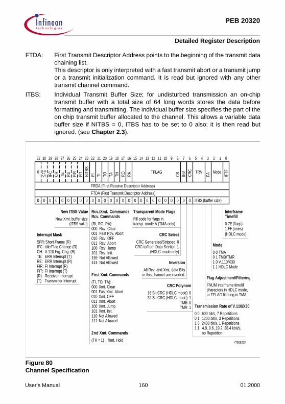
PEB 20320
Detailed Register Description
FTDA: First Transmit Descriptor Address points to the beginning of the transmit datachaining list.This descriptor is only interpreted with a fast transmit abort or a transmit jumpor a transmit initialization command. It is read but ignored with any othertransmit channel command.
ITBS: Individual Transmit Buffer Size; for undisturbed transmission an on-chiptransmit buffer with a total size of 64 long words stores the data beforeformatting and transmitting. The individual buffer size specifies the part of theon chip transmit buffer allocated to the channel. This allows a variable databuffer size if NITBS = 0, ITBS has to be set to 0 also; it is then read butignored. (see Chapter 2.3).
Figure 80Channel Specification
ITS08223
0 0 0 0 0 0 0 0 0 0 0 0 0 0 0 0 0 0 0 0 0 0 0 0 0 0
FRDA (First Receive Descriptor Address)
FTDA (First Transmit Descriptor Address)
0 TFLAG TRV Mode
31 30 29 28 27 26 25 24 23 22 21 20 19 18 17 16 15 14 13 12 11 10 9 8 7 6 5 4 3 2 1 0
SFE
IFC
CH TE RE FIR
FIT
NITB
SRI TI TO TA TH RO RA IF
TF
FACRC
INV
CS
Interrupt Mask
New ITBS Value
New Xmt. buffer size(ITBS valid)
Rcv./Xmt.Rcv. Commands
(RI, RO, RA):000 Rcv. Clear
Rcv. OFF010Rcv. Abort011Rcv. Jump100Rcv. Init.101Not Allowed110Not Allowed111
First Xmt. Commands
(TI, TO, TA):
IFC:CH:TE:RE:FIR:FIT:(R)(T) Transmitter Interrupt
Receiver Interrupt
Idle/Flag Change (R)V.110 Frg. Chg. (R)ERR Interrupt (T)ERR Interrupt (R)
FI Interrupt (T)
2
(TH = 1) Xmt. Hold
Transparent Mode Flags
Fill code for flags intransp. mode A (TMA only)
CRC Select
01
CRC Generated/StrippedCRC to/from Data Section
(HDLC mode only)
Inversion
All Rcv. and Xmt. data Bitsin this channel are inverted.
CRC Polynom
01
16 Bit CRC (HDLC mode)
TMBTMR 1
0
InterframeTimefill
01
7EFF
Mode
0 0 TMA0 1 TMB/TMR1 0 V.110/X301 1 HDLC Mode
Flag Adjustment/Filtering
FNUM interframe timefillcharacters in HDLC mode,or TFLAG filtering in TMA
Transmission Rate of V.110/X30
0 0 0 11 01 1
600 bit/s, 7 Repetitions
4.8, 9.6, 19.2, 38.4 kbit/s,no Repetition
ITBS (buffer size)
(ones)(flags)
(HDLC mode)
Short Frame (R)SFR:
Commands
001 Fast Rcv. Abort
FI Interrupt (R)
Fast Xmt. Abort001
111 Not Allowed110 Not Allowed101100011010 Xmt. OFF
Xmt. Clear000
Xmt. AbortXmt. JumpXmt. Init.
nd Xmt. Commands
:
32 Bit CRC (HDLC mode)
1200 bit/s, 3 Repetitions2400 bit/s, 1 Repetitions
User’s Manual 160 01.2000

PEB 20320
Detailed Register Description
4.2.6 Current Receive and Transmit Descriptor Address
For easier monitoring of the link lists the addresses of the just processed descriptors arewritten into the CCS. MUNICH32 changes the current descriptor address at the sametime when it branches to the next descriptor.
31 16 15 0
Current Receive Descriptor Address Channel 0
.
.
.
Current Receive Descriptor Address Channel 31
Current Transmit Descriptor Address Channel 0
.
.
.
Current Transmit Descriptor Address Channel 31
User’s Manual 161 01.2000
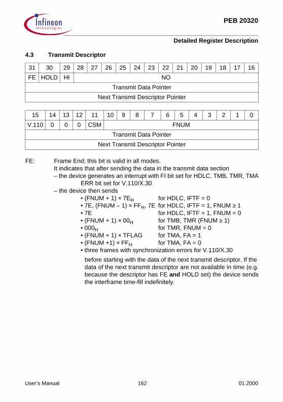
PEB 20320
Detailed Register Description
4.3 Transmit Descriptor
FE: Frame End; this bit is valid in all modes.It indicates that after sending the data in the transmit data section– the device generates an interrupt with FI bit set for HDLC, TMB, TMR, TMA
ERR bit set for V.110/X.30– the device then sends
• (FNUM + 1) × 7EH for HDLC, IFTF = 0• 7E, (FNUM – 1) × FFH, 7E for HDLC, IFTF = 1, FNUM ≥ 1• 7E for HDLC, IFTF = 1, FNUM = 0• (FNUM + 1) × 00H for TMB, TMR (FNUM ≥ 1)• 000H for TMR, FNUM = 0• (FNUM + 1) × TFLAG for TMA, FA = 1• (FNUM +1) × FFH for TMA, FA = 0• three frames with synchronization errors for V.110/X.30
before starting with the data of the next transmit descriptor. If the data of the next transmit descriptor are not available in time (e.g.because the descriptor has FE and HOLD set) the device sendsthe interframe time-fill indefinitely.
31 30 29 28 27 26 25 24 23 22 21 20 19 18 17 16
FE HOLD HI NO
Transmit Data Pointer
Next Transmit Descriptor Pointer
15 14 13 12 11 10 9 8 7 6 5 4 3 2 1 0
V.110 0 0 0 CSM FNUM
Transmit Data Pointer
Next Transmit Descriptor Pointer
User’s Manual 162 01.2000

PEB 20320
Detailed Register Description
HOLD: If the MUNICH32 detects a hold bit it– generates an interrupt with ERR bit set if FE = 0 or V.110/X.30 mode– sends the data in the current transmit data section– generates the FCS bits for HDLC and CS = 0 and CSM = 0– the device then sends at least
• (FNUM + 1) × 7EH for HDLC, IFTF = 0• 7E, FNUM × FFH for HDLC, IFTF = 1• (FNUM + 1) × 00H for TMB, TMR (FNUM ≥ 1)• 0000H for TMR, FNUM = 0• (FNUM + 1) × TFLAG for TMA, FA = 1• (FNUM + 1) × FFH for TMA, FA = 0• three frames with synchronization errors for V.110/X.30.
– It polls the HOLD bit and the next transmit descriptor address, but does nobranch to a new descriptor until the HOLD bit is reset. The next transmitdescriptor address is read but not interpreted as long as HOLD = 1.Therefore it can be changed together with setting HOLD = 0.The polling occurs at most every 8 valid clock cycles of the channel andcorresponds with internal requests from TF to TB.
– The device sends interframe time-fill until HOLD = 0 is polled.The HOLD condition is also discarded if a transmit jump, fast transmit abortor transmit initialization command is detected during the polling. TheMUNICH32 then branches to the transmit descriptor determined by FTDAeven though the HOLD bit of the current transmit descriptor may still be ‘1’.
HI: Host initiated Interrupt; if the HI bit is set, MUNICH32 generates an interruptwith set HI bit after transferring all data bytes.
NO: This byte number defines the number of bytes stored in the data section to betransmitted. A transmit descriptor and the corresponding data section mustcontain at least either one data byte or a frame end indication.Otherwise an interrupt with set ERR bit is generated.
V.110: This bit indicates that in the corresponding data section the E-, S- and X-bitsof the following V.110/X.30 frame are stored. MUNICH32 reads these bits andinserts them into the next possible V.110/X.30 frame. The data section maycontain only two bytes specified in the next figure.The first transmit descriptor after a transmit initialization channel commandmust have this bit set if it revives the channel from a transmit off condition orafter a pulse at the reset pin.
User’s Manual 163 01.2000
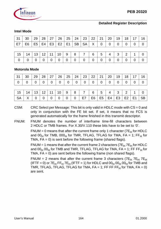
PEB 20320
Detailed Register Description
Intel Mode
Motorola Mode
CSM: CRC Select per Message: This bit is only valid in HDLC mode with CS = 0 andonly in conjunction with the FE bit set. If set, it means that no FCS isgenerated automatically for the frame finished in this transmit descriptor.
FNUM: FNUM denotes the number of interframe time-fill characters between2 HDLC or TMB frames. For X.30/V.110 these bits have to be set to ‘0’.
FNUM = 0 means that after the current frame only 1 character (7EH for HDLCand 00H for TMB, 000H for TMR, TFLAG, TFLAG for TMA, FA = 1; FFH forTMA, FA = 0) is sent before the following frame (shared flags).
FNUM = 1 means that after the current frame 2 characters (7EH 7EH for HDLCand 00H 00H for TMB and TMR, TFLAG, TFLAG for TMA, FA = 1; FF FFH forTMA, FA = 0) are sent before the following frame (non shared flags).
FNUM = 2 means that after the current frame 3 characters (7EH 7EH 7EH(IFTF = 0) or 7EH FFH 7EH (IFTF = 1) for HDLC and 00H 00H 00H for TMB andTMR, TFLAG, TFLAG, TFLAG for TMA, FA = 1; FF FF FFH for TMA, FA = 0)are sent.
31 30 29 28 27 26 25 24 23 22 21 20 19 18 17 16
E7 E6 E5 E4 E3 E2 E1 SB SA X 0 0 0 0 0 0
15 14 13 12 11 10 9 8 7 6 5 4 3 2 1 0
0 0 0 0 0 0 0 0 0 0 0 0 0 0 0 0
31 30 29 28 27 26 25 24 23 22 21 20 19 18 17 16
0 0 0 0 0 0 0 0 0 0 0 0 0 0 0 0
15 14 13 12 11 10 9 8 7 6 5 4 3 2 1 0
SA X 0 0 0 0 0 0 E7 E6 E5 E4 E3 E2 E1 SB
User’s Manual 164 01.2000

PEB 20320
Detailed Register Description
FNUM = k means that after the current frame k + 1 characters are sent(k + 1) times 7EH for ITFT = 0 and HDLC7EH, (k – 1) times FFH, 7EH for ITFT = 1 and HDLC(k + 1) times 00H for TMB, TMR(k + 1) times TFLAG for TMA, FA = 1(k + 1) times FFH for TMA, FA = 0.For HDLC mode FNUM is reduced by one eight of the number of zeroinsertions if FA is set. If the reduction would result in a negative number ofinterframe time-fill characters it is set to 0.
Transmit Data Pointer: This 32-bit pointer contains the start address of the transmit datasection. Although MUNICH32 works only long word oriented, itis possible to begin a transmit data section at an unevenaddress. The two least significant bits (ADD) of the transmit datapointer determine the beginning of the data section and thenumber of data bytes in the first long word of the data section,respectively.
ADD: 00 = 4 bytes01 = 3 bytes10 = 2 bytes11 = 1 byte
MUNICH32 reads the first long word and discards the unusedleast significant bytes. The NO establishes (determines) the endof the data section, whereas the remainder ofI (NO ADD) ÷ 4 I defines the number of bytes in the lastlong word of the data section.
MUNICH32 reads the last long word and discards the unusedmost significant bytes of the last long word.
If the first access is the same as the last access, ADD specifiesthe beginning of the data section and NO the number of databytes in the long word. All unused bytes are discarded.
User’s Manual 165 01.2000

PEB 20320
Detailed Register Description
For example (Intel mode):1) ADD = 01, NO = 8
2) ADD = 00, NO = 8
3) ADD = 10, NO = 1
For example (Motorola-mode):1) ADD = 01, NO = 8
2) ADD = 00, NO = 8
3) ADD = 10, NO = 1
11 10 01 00
byte 2 byte 1 byte 0 –
byte 6 byte 5 byte 4 byte 3 3 long words are read
– – – byte 7
11 10 01 00
byte 3 byte 2 byte 1 byte 0
byte 7 byte 6 byte 5 byte 4 2 long words are read
– – – –
11 10 01 00
– byte 0 – –
– – – – 1 long word is read!
– – – –
11 10 01 00
– byte 0 byte 1 byte 2
byte 3 byte 4 byte 5 byte 6 3 long words are read
byte 7 – – –
11 10 01 00
byte 0 byte 1 byte 2 byte 3
byte 4 byte 5 byte 6 byte 7 2 long words are read
11 10 01 00
– – byte 0 – 1 long word is read!
User’s Manual 166 01.2000

PEB 20320
Detailed Register Description
Next Transmit This 32-bit pointer contains the start address of the next transmitDescriptor Pointer: descriptor. After sending the indicated number of data bytes,
MUNICH32 branches to the next transmit descriptor to continuetransmission. The transmit descriptor is read entirely at thebeginning of transmission and stored in an on-chip memory.Therefore all information in the next descriptor must be validwhen MUNICH32 branches to this descriptor when HOLD = 0.For HOLD = 1 the next transmit descriptor pointer is polledtogether with HOLD; the next transmit descriptor must be valid,when HOLD = 0 is polled.
This pointer is not used if a transmit jump, fast transmit abort ortransmit initialization channel command is detected while theMUNICH32 still reads data from the current transmit descriptoror polls the HOLD bit. In this case FTDA is used as a pointer forthe next transmit descriptor to be branched to.
User’s Manual 167 01.2000

PEB 20320
Detailed Register Description
4.4 Receive Descriptor
The receive descriptor contains 4 long words; the first, third and fourth have to be writtenby the CPU, the second is written by the MUNICH32 when it branches to the next receivedescriptor or when it starts polling the HOLD bit.
Note: The MUNICH32 branches to a next descriptor without writing the second longword if the receive initialization command is used during normal operation (seeChapter 4.2.4)
HOLD: Setting the HOLD bit by the host prevents the device from branching to thenext descriptor. The current data section is still filled.
– Afterwards the second descriptor long word is written by the MUNICH32.For HDLC, TMB, TMR the FE and C-bit is set. If the frame could notcompletely be stored into the data section the RA bit is set in the status.An interrupt with set FI bit is generated, and in case the frame was aborted,the ERR bit is also set.For TMA, V.110/X.30 the C-bit and the RA bit is set and an interrupt withset ERR but with FI = 0 is generated.
– Afterwards the device starts polling the HOLD bit, received data, andreceived events normally leading to interrupts (with RT = 1) are discardeduntil HOLD = 0 is polled. Each 1 … 4 byte data word or interrupt eventnormally leading to an access now results in a poll cycle.Whenever HOLD = 1 is polled the next receive descriptor address is readbut ignored.
– When HOLD = 0 is polled• for HDLC, TMB, TMR the device continues to discard data until the end
of a received frame or an event leading to an interrupt (with RT = 1) is
31 30 29 28 27 26 25 24 23 22 21 20 19 18 17 16
0 HOLD HI NO
FE C 0 BNO
Receive Data Pointer
Next Receive Descriptor Pointer
15 14 13 12 11 10 9 8 7 6 5 4 3 2 1 0
0 0 0 0 0 0 0 0 0 0 0 0 0 0 0 0
Status 0 0 0 0 0 0 0 0
Receive Data Pointer
Next Receive Descriptor Pointer
User’s Manual 168 01.2000

PEB 20320
Detailed Register Description
detected. Afterwards the next received frame is transferred into the nextreceive descriptor. Interrupts are also generated again.
• For V.110/X.30, TMA the device puts the next data into the next receivedescriptor. Interrupts are also generated again.
The HOLD condition is also discarded upon detection of a receive jump, fastreceive abort or receive initialization command. The MUNICH32 thenbranches to the receive descriptor determined by FRDA even though theHOLD bit in the current receive descriptor may still be ‘1’.
HI: Host initiated interrupt; if the HI bit is set, MUNICH32 generates an interruptwith set HI bit after receiving all data bytes.
NO: This byte number defines the size of the receive data section allocated by thehost. Because MUNICH32 always writes long words the number of bytes(data section size) must be a multiple of 4 and greater or equal to 4. Themaximum data section size is 8188 bytes.
After reception of an HDLC frame with a data byte number not divisible by 4MUNICH32 first transfers the greatest entire ([number of data bytes/4]) in longwords. Then the remainder of the data bytes is transferred in another longword, where the non-significant bytes are filled with random values. Theyshould not be interpreted.
For example a HDLC frame with one data byte is received:
The data bytes are stored into the receive data section according to the LittleEndian convention (Intel mode) or Big Endian convention (Motorola mode).
FE: Frame End: The frame end bit is ‘1’ only in HDLC, TMB, TMR mode andindicates that a receive frame has ended in this receive descriptor. For TMA,V.110/X.30 the bit is always ‘0’.
FE = 0 in HDLC, TME, TMR mode means that frame continues in the nextreceive descriptor or that it filled the current receive data section exactly (BNO= NO). In this case the next receive descriptor will have FE = 1, C = 1, BNO= 0 and no data bytes are stored in the corresponding data section.
C: This bit is set by MUNICH32 if• it completes filling the data section normally (BNO = NO) ⇒ FE = 0,
status = 00• it was aborted by a fast receive abort channel command ⇒ status = 02
00000000.00001000.00000000.00000
11000000.00000001.Status.00000000
receive data pointer
next receive descriptor pointer
Receive Descriptor
XX.XX.XX.data
Receive Data Section
User’s Manual 169 01.2000
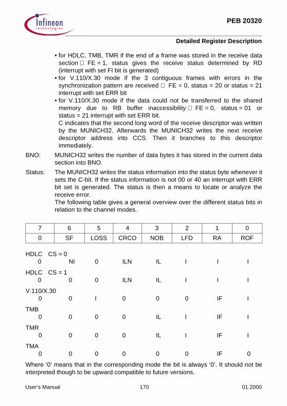
PEB 20320
Detailed Register Description
• for HDLC, TMB, TMR if the end of a frame was stored in the receive datasection ⇒ FE = 1, status gives the receive status determined by RD(interrupt with set FI bit is generated)
• for V.110/X.30 mode if the 3 contiguous frames with errors in thesynchronization pattern are received ⇒ FE = 0, status = 20 or status = 21interrupt with set ERR bit
• for V.110/X.30 mode if the data could not be transferred to the sharedmemory due to RB buffer inaccessibility ⇒ FE = 0, status = 01 orstatus = 21 interrupt with set ERR bit.C indicates that the second long word of the receive descriptor was writtenby the MUNICH32. Afterwards the MUNICH32 writes the next receivedescriptor address into CCS. Then it branches to this descriptorimmediately.
BNO: MUNICH32 writes the number of data bytes it has stored in the current datasection into BNO.
Status: The MUNICH32 writes the status information into the status byte whenever itsets the C-bit. If the status information is not 00 or 40 an interrupt with ERRbit set is generated. The status is then a means to locate or analyze thereceive error.The following table gives a general overview over the different status bits inrelation to the channel modes.
HDLC CS = 00 NI 0 ILN IL I I I
HDLC CS = 10 0 0 ILN IL I I I
V.110/X.300 0 I 0 0 0 IF I
TMB0 0 0 0 IL I IF I
TMR0 0 0 0 IL I IF I
TMA0 0 0 0 0 0 IF 0
Where ‘0’ means that in the corresponding mode the bit is always ‘0’. It should not beinterpreted though to be upward compatible to future versions.
7 6 5 4 3 2 1 0
0 SF LOSS CRCO NOB LFD RA ROF
User’s Manual 170 01.2000
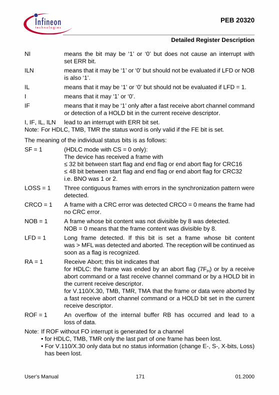
PEB 20320
Detailed Register Description
NI means the bit may be ‘1’ or ‘0’ but does not cause an interrupt withset ERR bit.
ILN means that it may be ‘1’ or ‘0’ but should not be evaluated if LFD or NOBis also ‘1’.
IL means that it may be ‘1’ or ‘0’ but should not be evaluated if LFD = 1.
I means that it may ‘1’ or ‘0’.
IF means that it may be ‘1’ only after a fast receive abort channel commandor detection of a HOLD bit in the current receive descriptor.
I, IF, IL, ILN lead to an interrupt with ERR bit set.Note: For HDLC, TMB, TMR the status word is only valid if the FE bit is set.
The meaning of the individual status bits is as follows:
SF = 1 (HDLC mode with CS = 0 only):The device has received a frame with≤ 32 bit between start flag and end flag or end abort flag for CRC16≤ 48 bit between start flag and end flag or end abort flag for CRC32i.e. BNO was 1 or 2.
LOSS = 1 Three contiguous frames with errors in the synchronization pattern weredetected.
CRCO = 1 A frame with a CRC error was detected CRCO = 0 means the frame hadno CRC error.
NOB = 1 A frame whose bit content was not divisible by 8 was detected.NOB = 0 means that the frame content was divisible by 8.
LFD = 1 Long frame detected. If this bit is set a frame whose bit contentwas > MFL was detected and aborted. The reception will be continued assoon as a flag is recognized.
RA = 1 Receive Abort; this bit indicates thatfor HDLC: the frame was ended by an abort flag (7FH) or by a receiveabort command or a fast receive channel command or by a HOLD bit inthe current receive descriptor.for V.110/X.30, TMB, TMR, TMA that the frame or data were aborted bya fast receive abort channel command or a HOLD bit set in the currentreceive descriptor.
ROF = 1 An overflow of the internal buffer RB has occurred and lead to aloss of data.
Note: If ROF without FO interrupt is generated for a channel• for HDLC, TMB, TMR only the last part of one frame has been lost.• For V.110/X.30 only data but no status information (change E-, S-, X-bits, Loss)
has been lost.
User’s Manual 171 01.2000
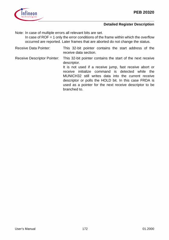
PEB 20320
Detailed Register Description
Note: In case of multiple errors all relevant bits are set.In case of ROF = 1 only the error conditions of the frame within which the overflowoccurred are reported. Later frames that are aborted do not change the status.
Receive Data Pointer: This 32-bit pointer contains the start address of thereceive data section.
Receive Descriptor Pointer: This 32-bit pointer contains the start of the next receivedescriptor.It is not used if a receive jump, fast receive abort orreceive initialize command is detected while theMUNICH32 still writes data into the current receivedescriptor or polls the HOLD bit. In this case FRDA isused as a pointer for the next receive descriptor to bebranched to.
User’s Manual 172 01.2000

PEB 20320
Application Notes
5 Application Notes
5.1 Test Loops
5.1.1 Test Loop Definitions for the MUNICH32
Two basic types of test loops are provided by the MUNICH32, internal and external.Each of these types is further subdivided into channelwise and complete test loops thusproviding four possible test loops.
5.1.1.1 Internal Complete Test Loop
The serial data output is physically routed to the serial data input. The TX data appearson the TDATA output pin and the RDATA input pin is ignored. TCLK and RCLK have tobe identical; TSP and RSP have to be identical. The logical Transmit and Receivechannels have to be programmed identically.
Figure 81
ITS08198
TDATA
1
&
CD
RDATA
µP Interface
Enable Int.Complete Loop
&
RSPRCLK
TCLKTSP
User’s Manual 173 01.2000

PEB 20320
Application Notes
5.1.1.2 Internal Channelwise Test Loop
One (and only one) logical channel is mirrored from the serial data output to the serialdata input. The other logical channels are not affected by this operation. The transmitand receive data rates for this single logical channel must be identical. Normal TCLK,RCLK, TSP and RSP design rules apply. This test loop provides channelwise testingcapabilities during idle channel time slots, without interfering with normal datatransmission/reception.
Figure 82
5.1.1.3 External Complete Test Loop
The serial data input is physically routed to the serial data output. Data is received on theRDATA pin and routed to the TDATA pin. The received data can be stored in sharedmemory for additional diagnostic purposes. TCLK and RCLK have to be identical; TSPand RSP have to be identical.
ITS08199
TDATA
1
&
CD
Channel X only
RDATA
µP InterfaceEnable Int.Channelwise Loopfor Channel X
User’s Manual 174 01.2000
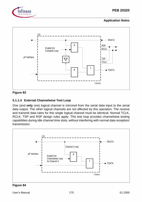
PEB 20320
Application Notes
Figure 83
5.1.1.4 External Channelwise Test Loop
One (and only one) logical channel is mirrored from the serial data input to the serialdata output. The other logical channels are not affected by this operation. The receiveand transmit data rates for this single logical channel must be identical. Normal TCLK,RCLK, TSP and RSP design rules apply. This test loop provides channelwise testingcapabilities during idle channel time slots, without interfering with normal data reception/transmission.
Figure 84
ITS08200
TDATA1
&
CD
RDATA
µP Interface
Enable Ext.Complete Loop
&
RSPRCLK
TCLKTSP
ITS08201
TDATA1
&
CD
Channel X only
RDATA
µP InterfaceEnable Ext.Channelwise Loopfor Channel X
User’s Manual 175 01.2000

PEB 20320
Application Notes
5.1.2 Test Loop Activation
All of the test loops are closed (activated) and opened (deactivated) by setting/resettingthe appropriate combination of bits in the Action Specification (Table 10). Any unlistedcombination of LOC, LOOP and LOOPI is an invalid operation. Although the data sheet(Data Sheet 08.93) specifically states that loops must be left (opened) by issuing thereset pin to ‘1’, there are exceptions to this rule. Generally, the test loops can be openedby software. There are several cases that must be examined and these will be discussedin the next section.
When closing (activating) a test loop, the IN, ICO, IM, RES, and IA bits should equal ‘0’and PCM and MFL should be set to the appropriate values.
The following recommended procedure for activating a test loop assumes that theMUNICH32 has been fully initialized and the user desires to activate a test loop onchannel x:
• Initialize Rc and Tx channel as appropriate for type of test loop.• Close (activate) the test loop.• Perform test functions (transmit/receive data, check for interrupts, errors, etc.)• Open (deactivate) the test loop.• Perform Rc and Tx off function.Note: While the test loop is activated, do not execute the transmit off command. It will
not have the effect of resetting the transmit formatter.
5.1.3 Test Loop Deactivation and Switching
As mentioned previously, a test loop can be opened (deactivated) by software. Todeactivate a test loop a new ASP should be issued with LOC, LOOP, and LOOPI = 0 andall other bits should be set to the previous values used during activation. Listed beloware the possible test loop operations that can be activated with software and thoserequiring a hardware reset. Table 11 is provided as a graphical representation of thisinformation.
Table 10Test Loop Activation
Test Loop LOC LOOP LOOPI ASP
Internal complete 0 0 1 xxxxxx08H
Internal channelwise 1 0 1 xxxxxx28H
External complete 0 1 0 xxxxxx10H
External channelwise 1 1 0 xxxxxx30H
No loop 0 0 0 xxxxxx00H
User’s Manual 176 01.2000

PEB 20320
Application Notes
5.1.3.1 Software Operations
Close and open internal complete loop.Close and open internal channelwise loop.Close and open external complete loop.Close and open external channelwise loop.Change from internal complete loop to internal channelwise loop.Change from external complete loop to external channelwise loop.
5.1.3.2 Hardware Reset Operations
Change between the internal complete loop and external complete loop.Change between the internal channelwise loop and external channelwise loop.Change between the internal channelwise loop and internal complete loop.Change between the external channelwise loop and external complete loop.Change between internal channelwise loop and external complete loop.Change between internal complete loop and external channelwise loop.Change between external channelwise loop and internal complete loop.Change between external complete loop and internal channelwise loop.
Table 11Allowed Operations
Change to
Internal Complete Loop
Internal Channelwise Loop
External Complete Loop
External Channelwise Loop
Internal Complete Loop
X SFW HDW Reset required
HDW Reset required
Internal Channelwise Loop
HDW Reset required
X HDW Reset required
HDW Reset required
External Complete Loop
HDW Reset required
HDW Reset required
X SFW
External Channelwise Loop
HDW Reset required
HDW Reset required
HDW Reset required
X
User’s Manual 177 01.2000

PEB 20320
Application Notes
5.1.4 Test Loop Examples
5.1.4.1 Internal Channelwise Test Loop
Generate HW RESET, and hold off RSP/TSP for 1000 SCLK cycles.ASP: A104-8004 ;CEPT, MFL=260, IN, IA=1IQS: ICQ
0000-001FTSA[0]: 00FF-00FF ;TS0 = CH0TSA[1…31]: 0000-0000 (×31)CSP[0]: 00E9-0006 ;Tx/Rc init, poll Tx Desc, HDLC
FRDAFTDA0000-0002 ;ITBS = 2 long words
CSP[1…31] 0000-0000 0000-0000 0000-0000 0000-0000 (x31)CRA[0…31] 0000-0000 (×32)CTA[0…31] 0000-0000 (×32)
ICQ: 0000-0000 (×512)
FRDA: 0020-00000000-0000RcvDtaPtr → 32 byte
+ NxtRDPtr data block+→ 0020-0000
0000-0000RcvDtaPtr → 32 byte
+ NxtRDPtr data block+→ 0020-0000
0000-0000RcvDtaPtr → 32 byte
+ NxtRDPtr data block+→ 4020-0000 ;HOLD = 1
0000-0000RcvDtaPtr → 32 byte0000-0000 data block
FTDA: C000-0000 ; HOLD, FE = 1 for dummy frameXmtDtaPtr
+ NxtTDPtr+→ 0020-0000
XmtDtaPtr → abcdefghijklmnop+ NxtTDPtr qrstuvwxyz012345+→ C020-0000 ;FE, HOLD = 1
XmtDtaPtr → ABCDEFGHIJKLMNOP0000-0000 QRSTUVWXYZ987654
User’s Manual 178 01.2000

PEB 20320
Application Notes
Generate AR Pulse and wait for INT signal (set up TS0 and CH0).
Read interrupt queue:ICQ: 9000-8000 ;Action Request Acknowledge
;V2.2 (V2.1 = 8800-8000)9000-1000 ;Polls HOLD bit of 1st Tx Desc.
Set ASP for Internal Channelwise Loop testASP: A104-0028 ;CEPT, MFL=260, Int. Chnl loop
Generate AR Pulse and wait for INT signal.
Read interrupt queue:ICQ: 9000-8000 ;Action Request Acknowledge
9000-1000 ;Polls HOLD bit of 1st Tx Desc.9000-082020 ;Rc ITF state change
Clear HOLD bit in FTDA (allow frame to Tx over Internal Chnl. Loop).
Read interrupt queue:ICQ: 9000-1000 ;End of Tx frame, polling HOLD
bit of Tx desc.9000-1020 ;Rc frame complete
Read receive descriptors:FRDA: 0020-0000
4020-0000 ;C = 1, NO = BNORcvDtaPtr → abcdefghijklmnop
+ NxtRDPtr qrstuvwxyz012345+→ 0020-0000
4020-0000 ;C = 1, NO=BNORcvDtaPtr → ABCDEFGHIJKLMNOP
+ NxtRDPtr QRSTUVWXYZ987654+→ 0020-0000
C000-0000 ;FE, C = 1, BNO = 0RcvDtaPtr → ;empty! (p. 139 User’s Manual -
FE description)+ NxtRDPtr+→ 4020-0000
0000-0000RcvDtaPtr → 32 byte0000-0000 data block
User’s Manual 179 01.2000
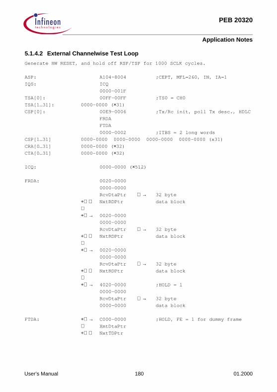
PEB 20320
Application Notes
5.1.4.2 External Channelwise Test Loop
Generate HW RESET, and hold off RSP/TSP for 1000 SCLK cycles.
ASP: A104-8004 ;CEPT, MFL=260, IN, IA=1
IQS: ICQ
0000-001F
TSA[0]: 00FF-00FF ;TS0 = CH0
TSA[1…31]: 0000-0000 (×31)CSP[0]: 00E9-0006 ;Tx/Rc init, poll Tx desc., HDLC
FRDA
FTDA
0000-0002 ;ITBS = 2 long words
CSP[1…31] 0000-0000 0000-0000 0000-0000 0000-0000 (x31)
CRA[0…31] 0000-0000 (×32)CTA[0…31] 0000-0000 (×32)
ICQ: 0000-0000 (×512)
FRDA: 0020-0000
0000-0000
RcvDtaPtr → 32 byte
+ NxtRDPtr data block
+→ 0020-0000
0000-0000
RcvDtaPtr → 32 byte
+ NxtRDPtr data block
+→ 0020-0000
0000-0000
RcvDtaPtr → 32 byte
+ NxtRDPtr data block
+→ 4020-0000 ;HOLD = 1
0000-0000
RcvDtaPtr → 32 byte
0000-0000 data block
FTDA: +→ C000-0000 ;HOLD, FE = 1 for dummy frame
XmtDtaPtr
+ NxtTDPtr
User’s Manual 180 01.2000

PEB 20320
Application Notes
Generate AR Pulse and wait for INT signal (set up TS0 and CH0).
Read interrupt queue:
ICQ: 9000-8000 ;Action Request Acknowledge
;V2.2 (V2.1 = 8800-8000)
9000-1000 ;Polls HOLD bit of 1st Tx Desc.
9000-1000 ;FI Frame indication for the
1st Tx Desc.
;Now M32 starts polling HOLD
bit of 1st Desc.
Set ASP for External Channelwise test loop
ASP: A104-0030 ;CEPT, MFL=260, Ext. Chnl loop
Generate AR Pulse and wait for INT signal.
Read interrupt queue:
ICQ: 9000-8000 ;Action Request Acknowledge
9000-0820 ;Only if other station uses
idle code 7E
9000-1020 ;Received frame complete
Read receive descriptors: ;assumes 64 byte frame externally looped
FRDA: 0020-0000 ;with proper HDLC framing
4020-0000 ;NO = BNO
RcvDtaPtr → abcdefghijklmnop
+ NxtRDPtr qrstuvwxyz012345
+→ 0020-0000
4020-0000 ;NO=BNO
RcvDtaPtr → ABCDEFGHIJKLMNOP
+ NxtRDPtr QRSTUVWXYZ987654
+→ 0020-0000
C000-0000 ;FE, C = 1, BNO = 0
RcvDtaPtr → ;empty!
+ NxtRDPtr
+→ 4020-0000
0000-0000
RcvDtaPtr → 32 byte
0000-0000 data block
User’s Manual 181 01.2000

PEB 20320
Application Notes
5.2 MUNICH32 in a LAN/WAN Router
5.2.1 Introduction
Subject of this application note is an ISDN/LAN Router, a communication system thatenables two LANs to communicate via the ISDN.
Figure 85ISDN/LAN Router
The structure of the whole system is shown in Figure 85. The router itself is realized asa stand alone solution. It is connected to a standard PC for software download andmaintenance control only. After the download the system works fully independent of thehost PC.
The hardware of the ISDN/LAN router consists of an application specific part and aprocessor system. The application specific hardware is mainly based on the SIEMENSComponent MUNICH32 (Multi Channel Network Interface Controller for HDLC) and astandard LAN controller. Both devices are integrated in the same processor system.
The software of the ISDN/LAN router is formed by integrating the MUNICH32 DeviceDriver Module (DDM) and the corresponding LAN controller Device Driver Module in aDevice Driver System (DDS). The device driver modules build a platform to implementthe routing strategy in a separate application module.
The application specific hardware, the MUNICH32 Device Driver Module and theapplication module are the main aspects described in the following chapters. Thestructure of the processor system is briefly illustrated. The DDS service routines areexplained as far as necessary to understand this special application. It is suggested thatthe reader has some knowledge about the MUNICH32 before reading this applicationnote. Detailed information about the MUNICH32, its features and memory structures aregiven in the MUNICH32 PEB20320 Data Sheet.
ITS08283
Router RouterISDN
LAN LAN
User’s Manual 182 01.2000

PEB 20320
Application Notes
5.2.2 Hardware
The processor system is based on a Motorola 68040 processor. It contains 512 KByteSRAM, a bus controller and peripherals like timer, EPROM and interrupt controller. Theapplication specific hardware is integrated by using a Peripheral Connector and anAlternate Busmaster Connector. The Peripheral Connector allows the integration ofexternal peripherals. The Alternate Busmaster Connector is used to connect externalbus masters to the local bus. The system is provided with a RS232 serial interface todownload executable software on the board.
Figure 86Hardware Block Diagram
ITB08284
Timer
EPROM
InterruptController
SRAM
AlternateBusmasterConnector
PeripheralConnector
BusController
MC68040
i82596 MUNICH32
i82C501
EM 2
Connector Connector
ACFA
PRACT
RS232
ISDNInterface Interface
LAN
Glue Logic
LAN ISDN
User’s Manual 183 01.2000

PEB 20320
Application Notes
Application Specific Hardware
The application specific hardware consists of an ISDN primary rate interface and anEthernet interface. The MUNICH32 PEB 20320 in conjunction with the layer 1 SIEMENScomponents ACFA (Advanced CMOS Frame Aligner) PEB 2035 and PRACT (PrimaryRate Access Clock Generator and Transceiver) PEB 22320 are used to build the primaryrate interface. Incoming data from the ISDN is first processed from the PRACT. Ittranslates the HDB3 coded line signals in dual rail signals. The PRACT also suppliesACFA and MUNICH32 with clock signals. Main task of the ACFA is the frame alignment.Besides, the ACFA translates the dual rail data in a single rail, unipolar bit stream whichcan be processed by the MUNICH32.
The MUNICH32 handles up to 32 channels of a full duplex PCM highway. All time-slotsmay have data rates between 8 Kbit/s and 64 Kbit/s. The MUNICH32 supports besidesother protocols the HDLC formatting/deformatting. If programmed for HDLC mode, theMUNICH32 performs HDLC specific functions like framing, CRC check/generation,flag stuffing and zero bit insertion/deletion autonomously. An on-chip 64-channelDMA controller allows the device to store/read data into/from the SRAM. The DMAcontroller manages long word or word transfers via a 32-bit processor interface. TheµP interface can be configured to be Motorola 68020 or intel 80386 compatible.
Figure 87ISDN Interface
The Ethemet interface is built with a LAN controller, a Manchester encoder/decoder anda transceiver. The LAN controller supports all IEEE 802.3 standards. The Ethernetframing: preamble generation, source address generation, destination addresschecking, short-frame detection, automatic length field handling is performed. AfterLAN controller processing the transmit data is Manchester encoded and forwarded to thetransmission line, while receive data is Manchester decoded before being processed bythe LAN controller.
ITS08285
MUNICH32 ACFA PRACTLine IN
Line OUT
OvervoltageµP Interface
PCMHighway
Dual RailUnipolarSignals
User’s Manual 184 01.2000

PEB 20320
Application Notes
System Architecture
The system architecture is shown in Figure 88. The MUNICH32, the CPU and theLAN controller store data in the shared memory. The communication between CPU andalternate bus master is done via the shared memory. The CPU informs the alternate busmasters with help of control signals about changes in the shared memory and vice versa.The MUNICH32 input control signal is the Action Request pulse (ACTION REQUEST).It is generated by one CPU write cycle to a defined address and decoding the addresslines. The MUNICH32 then responds by generating an interrupt pulse and writing therespective interrupt information in the SRAM.
Figure 88System Architecture
ITS08286
MUNICH32 CPU i82596
SignalsControl Control
Signals
Local Bus
SharedMemory
User’s Manual 185 01.2000
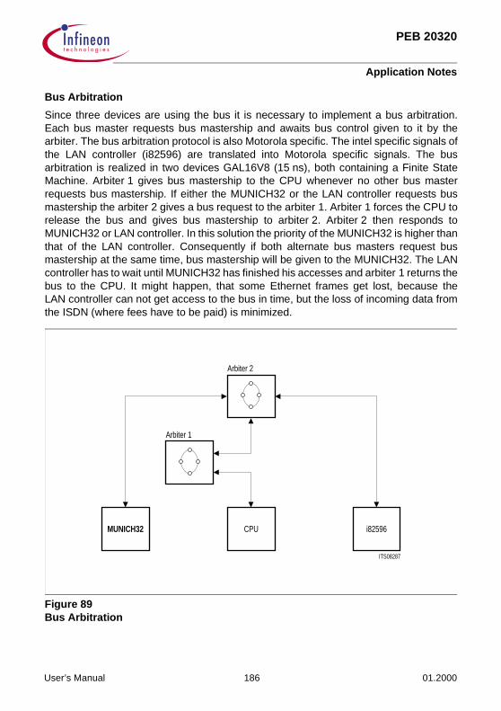
PEB 20320
Application Notes
Bus Arbitration
Since three devices are using the bus it is necessary to implement a bus arbitration.Each bus master requests bus mastership and awaits bus control given to it by thearbiter. The bus arbitration protocol is also Motorola specific. The intel specific signals ofthe LAN controller (i82596) are translated into Motorola specific signals. The busarbitration is realized in two devices GAL16V8 (15 ns), both containing a Finite StateMachine. Arbiter 1 gives bus mastership to the CPU whenever no other bus masterrequests bus mastership. If either the MUNICH32 or the LAN controller requests busmastership the arbiter 2 gives a bus request to the arbiter 1. Arbiter 1 forces the CPU torelease the bus and gives bus mastership to arbiter 2. Arbiter 2 then responds toMUNICH32 or LAN controller. In this solution the priority of the MUNICH32 is higher thanthat of the LAN controller. Consequently if both alternate bus masters request busmastership at the same time, bus mastership will be given to the MUNICH32. The LANcontroller has to wait until MUNICH32 has finished his accesses and arbiter 1 returns thebus to the CPU. It might happen, that some Ethernet frames get lost, because theLAN controller can not get access to the bus in time, but the loss of incoming data fromthe ISDN (where fees have to be paid) is minimized.
Figure 89Bus Arbitration
ITS08287
MUNICH32 CPU i82596
Arbiter 1
Arbiter 2
User’s Manual 186 01.2000
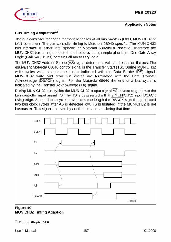
PEB 20320
Application Notes
Bus Timing Adaptation1)
The bus controller manages memory accesses of all bus masters (CPU, MUNICH32 orLAN controller). The bus controller timing is Motorola 68040 specific. The MUNICH32bus interface is either Intel specific or Motorola 68020/030 specific. Therefore theMUNICH32 bus timing needs to be adapted by using simple glue logic. One Gate ArrayLogic (Gal16V8, 15 ns) contains all necessary logic.
The MUNICH32 Address Strobe (AS) signal determines valid addresses on the bus. Theequivalent Motorola 68040 control signal is the Transfer Start (TS). During MUNICH32write cycles valid data on the bus is indicated with the Data Strobe (DS) signal.MUNICH32 write and read bus cycles are terminated with the Data TransferAcknowledge (DSACK) signal. For the Motorola 68040 the end of a bus cycle isindicated by the Transfer Acknowledge (TA) signal.
During MUNICH32 bus cycles the MUNICH32 output signal AS is used to generate thebus controller input signal TS. The TS is deasserted with the MUNICH32 input DSACKrising edge. Since all bus cycles have the same length the DSACK signal is generatedtwo bus clock cycles after AS is detected low. TS is tristated, if the MUNICH32 is notbusmaster. This signal is driven by another bus master during that time.
Figure 90MUNICH32 Timing Adaption
1) See also Chapter 5.2.6.
ITD08288
BCLK
SCLK
TS
TA
Addr
Data
AS
DSACK
User’s Manual 187 01.2000
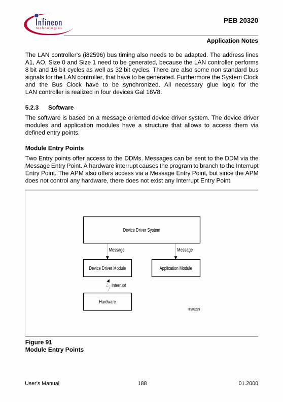
PEB 20320
Application Notes
The LAN controller’s (i82596) bus timing also needs to be adapted. The address linesA1, AO, Size 0 and Size 1 need to be generated, because the LAN controller performs8 bit and 16 bit cycles as well as 32 bit cycles. There are also some non standard bussignals for the LAN controller, that have to be generated. Furthermore the System Clockand the Bus Clock have to be synchronized. All necessary glue logic for theLAN controller is realized in four devices Gal 16V8.
5.2.3 Software
The software is based on a message oriented device driver system. The device drivermodules and application modules have a structure that allows to access them viadefined entry points.
Module Entry Points
Two Entry points offer access to the DDMs. Messages can be sent to the DDM via theMessage Entry Point. A hardware interrupt causes the program to branch to the InterruptEntry Point. The APM also offers access via a Message Entry Point, but since the APMdoes not control any hardware, there does not exist any Interrupt Entry Point.
Figure 91Module Entry Points
ITS08289
Device Driver System
Device Driver Module Application Module
Message Message
Hardware
Interrupt
User’s Manual 188 01.2000

PEB 20320
Application Notes
DDS Tasks
The message transfer between the modules is the main task of the DDS, realized bysome service routines. DDMs and APMs are integrated in the DDS by executing aModule Init Routine. The Module Init Routine is called by the DDS. Additionally the DDSoffers service routines for memory management. All service routines can be used by allmodules. Some memory management functions will be presented in more detail. Fordetailed information about the other DDS service routines please refer to the SIPB 7520Primary Rate User Board or EASY532 Datacom Userboard Documentation.
Memory Management
With the memory management functions the allocation of message descriptors,MUNICH32 receive/transmit descriptors1) or LAN controller receive/transmit descriptorsis simplified. During initialization of the memory management module DDSM a pool ofdescriptors is prepared in a linked list. The memory management functions allow toallocate descriptors and to free descriptors. During initialization of the memorymanagement module DDSM a pool of descriptors is prepared in a linked list. Thememory management functions allow to allocate descriptors and to free descriptors.During allocation a descriptor is taken from the prepared list. After utilization thedescriptor is given back to the descriptor pool. There is one pool for message descriptorsand one pool for MUNICH32 receive/transmit and LAN controller receive/transmitdescriptors. Because MUNICH32 transmit and receive descriptors differ and they bothdiffer from the LAN controller transmit and receive descriptors, there are servicefunctions available to convert the descriptor type.
1) Refer to MUNICH32 Data Sheet.
User’s Manual 189 01.2000

PEB 20320
Application Notes
Figure 92Memory Management
ITS08290
Message Descriptor PoolAllocate
Free
Free
Allocate
Conv
ert
MUNICH32/LAN ControllerDescriptor Pool
User’s Manual 190 01.2000
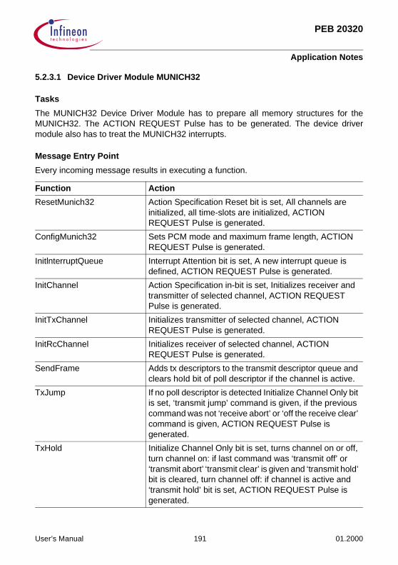
PEB 20320
Application Notes
5.2.3.1 Device Driver Module MUNICH32
Tasks
The MUNICH32 Device Driver Module has to prepare all memory structures for theMUNICH32. The ACTION REQUEST Pulse has to be generated. The device drivermodule also has to treat the MUNICH32 interrupts.
Message Entry Point
Every incoming message results in executing a function.
Function Action
ResetMunich32 Action Specification Reset bit is set, All channels are initialized, all time-slots are initialized, ACTION REQUEST Pulse is generated.
ConfigMunich32 Sets PCM mode and maximum frame length, ACTION REQUEST Pulse is generated.
InitlnterruptQueue Interrupt Attention bit is set, A new interrupt queue is defined, ACTION REQUEST Pulse is generated.
InitChannel Action Specification in-bit is set, Initializes receiver and transmitter of selected channel, ACTION REQUEST Pulse is generated.
InitTxChannel Initializes transmitter of selected channel, ACTION REQUEST Pulse is generated.
InitRcChannel Initializes receiver of selected channel, ACTION REQUEST Pulse is generated.
SendFrame Adds tx descriptors to the transmit descriptor queue and clears hoId bit of poll descriptor if the channel is active.
TxJump If no poll descriptor is detected Initialize Channel Only bit is set, ‘transmit jump’ command is given, if the previous command was not ‘receive abort’ or ‘off the receive clear’ command is given, ACTION REQUEST Pulse is generated.
TxHold Initialize Channel Only bit is set, turns channel on or off, turn channel on: if last command was ‘transmit off’ or ‘transmit abort’ ‘transmit clear’ is given and ‘transmit hold’ bit is cleared, turn channel off: if channel is active and ‘transmit hold’ bit is set, ACTION REQUEST Pulse is generated.
User’s Manual 191 01.2000

PEB 20320
Application Notes
Interrupt Entry Point
The information in the interrupt queue is read and a message containing that informationis sent to the user.
In case of a received frame the written receive descriptors are linked to a message andsent to the user. The next available descriptor in the list is linked to the memorystructures. An equivalent number of new receive descriptors is allocated and linked tothe end of the receive descriptor queue.
In case of a transmit acknowledge interrupt the used transmit descriptors are releasedto the descriptor pool.
TxShutDown Initialize Channel Only bit is set, gives ‘transmit off’ command or ‘transmit abort’ command, ACTION REQUEST Pulse is generated.
RcJump Initialize Channel Only bit is set, If last command was ‘transmit off’ or ‘transmit abort’ ‘transmit clear’ is given, ‘receive jump’ command is given, ACTION REQUEST Pulse is generated.
RcShutDown ‘Initialize Channel Only’ bit is set, Gives receive off command if receiver was aborted otherwise gives receive abort command, ACTION REQUEST Pulse is generated.
SwitchlnternalChanLoop Sets/clears Internal Channelwise Loop, ACTION REQUEST Pulse is generated.
SwitchlnternalCompLoop Sets/clears Complete Loop, ACTION REQUEST Pulse is generated.
ShowMunich32VersionNr ACTION REQUEST Pulse is generated.
CheckActionRequestQueue Looks for messages to be processed and branches to the Message Entry Point.
Function Action
User’s Manual 192 01.2000

PEB 20320
Application Notes
Programming the MUNICH32 for this Application
The basic programming of the MUNICH32 for this application is realized in the ModuleInitialization Routine. Further programming is done by calling the function ‘Init Channel’for each channel once. Transmit data is then added to the memory structures by passinga message with linked transmit descriptor(s) to the function ‘Send Frame’.
Module Initialization Routine
Here the IM-bit is cleared because the MUNICH32 DDM expects the action requestacknowledge interrupt. The values for PCM and MFL are set. The PCM format is a 32-channel format according to CEPT. The maximum frame length is set to its maximum.Finally the address and length of a new interrupt queue are defined. Those values willnot be changed anymore.
Init Channel Routine
The function ‘Init Channel’ initializes the time-slot assignment and the channelspecification for one channel. The channel number is set to the value of the variable‘channel’. The MUNICH32 is alerted to access all time-slot assignments and the channelspecification by setting the in-bit.
The fillmask (transmit and receive) for the selected channel is written in the appropriateword of the time-slot assignment. All other channels and their fillmasks are not affected.
For this application all interrupts are enabled. Initialization of the selected channelcomprises the definition of a new ITBS value and initialization of the receiver and thetransmitter. The transmit hold bit is cleared. After initialization the MUNICH32 startspolling the hold bit of the current transmit descriptor. Therefore a transmit descriptor isallocated and connected to the memory structures. Its hold bit and fe-bit are set to one,its no-bits are set to zero. For that reason the MUNICH32 does not transmit anything butpolls this descriptor. Since after the receiver’s initialization the MUNICH32 is ready toreceive data, a queue of receive descriptors is allocated and linked to the memorystructures. The hold bit of the last descriptor in the list is set to indicate the end of the list.In all other descriptors the hold bit is cleared.
User’s Manual 193 01.2000

PEB 20320
Application Notes
Send Frame Routine
Calling ‘SendFrame’ after initialization of a channel results in executing ‘AddHdlcFrame’.In that routine the transmit descriptors are disconnected from the message and linked tothe memory structures. If the message source is the ‘MROUTE Application Module’ thehold bit and fe-bit indicating the end of a frame and the end of the list have already beenset/cleared in the MROUTE module, they are not modified anymore. If the messagesource is any other module the fe-bit and hold bit are cleared in all descriptors except forthe last one. There the hold bit has to be set, to prevent the MUNICH32 from branchingto the next descriptor. Setting the fe-bit in the last descriptor only forces the MUNICH32to send the data in one HDLC frame. The bits HI, V110 and CSM are cleared in bothcases.
Transmit/Receive Interrupt
A transmit acknowledge interrupt is treated by returning the transmit descriptor(s) to thedescriptor pool.
After a receive interrupt (FI bit set) the receive descriptors with c-bit set, aredisconnected from the list of receive descriptors, linked to a message and sent to theMROUTE module. The next free receive descriptor in the list is linked to the memorystructures. An equivalent number of new descriptors is allocated and linked to the end ofthe receive descriptor list.
5.2.3.2 Application Module MROUTE
The application module MROUTE implements the routing strategy.
Routing Strategy
Both devices the MUNICH32 and the LAN controller organize receive and transmit datain a linked list of receive descriptors and a linked list of transmit descriptors. The data isstored in data buffers of variable size. The receive/transmit descriptors contain theaddress of the data buffer. The basic idea behind the routing strategy is, to take theMUNlCH32’s receive descriptor and link it to the LAN controller’s transmit descriptorqueue. On the other hand to take the LAN controller’s receive descriptor and link it to theMUNlCH32’s transmit descriptor queue.
User’s Manual 194 01.2000
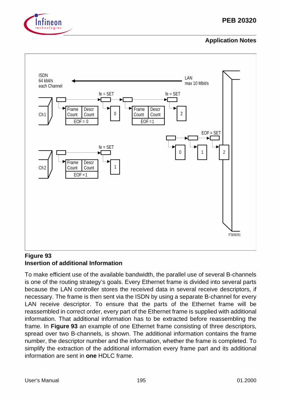
PEB 20320
Application Notes
Figure 93Insertion of additional Information
To make efficient use of the available bandwidth, the parallel use of several B-channelsis one of the routing strategy’s goals. Every Ethernet frame is divided into several partsbecause the LAN controller stores the received data in several receive descriptors, ifnecessary. The frame is then sent via the ISDN by using a separate B-channel for everyLAN receive descriptor. To ensure that the parts of the Ethernet frame will bereassembled in correct order, every part of the Ethernet frame is supplied with additionalinformation. That additional information has to be extracted before reassembling theframe. In Figure 93 an example of one Ethernet frame consisting of three descriptors,spread over two B-channels, is shown. The additional information contains the framenumber, the descriptor number and the information, whether the frame is completed. Tosimplify the extraction of the additional information every frame part and its additionalinformation are sent in one HDLC frame.
ITS08291
0FrameCount
DescrCount
EOF = 0 1=EOFCountDescr
CountFrame
2
fe = SET SET=fe
Ch1
2Ch
SET=fe
1=EOFCountDescr
CountFrame
1
0 1 2
EOF = SET
ISDN64 kbit/seach Channel max 10 Mbit/s
LAN
User’s Manual 195 01.2000

PEB 20320
Application Notes
The fe-bit marks the end of one HDLC frame, the EOF bit marks the end of the Ethernetframe. The additional information comprises the 8-bit word descriptor count, 16-bit wordframe count and EOF a 8-bit variable which indicates the last descriptor of the frame.
Message Entry Point
The message entry point calls two functions: IsdnRouteFrame and LanRouteFrame. AnEthernet frame is processed by IsdnRouteFrame, an ISDN frame by LanRouteFrame.The MUNICH32 receive descriptors are converted to LAN controller transmit descriptorsand those of the LAN controller are converted to MUNICH32 transmit descriptors.
Figure 94Message Flow between DDMs and MROUTE Module
Besides the IsdnRouteFrame realizes the insertion of additional information and splitsan Ethernet frame on several B-channels. The additional information is stored in an extraallocated transmit descriptor which is placed before the descriptor containing the data.Every descriptor and the respective extra descriptor are connected to one messagedescriptor. This message with set hold bit and set fe-bit in the descriptor containing thedata is further processed from the MUNICH32 DDM routine ‘Send Frame’.
LanRouteFrame reassembles the Ethernet frames. It takes into account, that the partsmight arrive with different delays. Every complete frame is connected to a messagedescriptor and than processed from the LAN controller DDM.
MUNICH32DDM DDM
LAN Controller
ISDN Route Frame
LAN Route Frame
MROUTE Module
MUNICH32TX Descr
RC DescrMUNICH32
Message Descr
TX DescrLAN Controller
RC DescrLAN Controller
Message Descr
ITS08292
User’s Manual 196 01.2000

PEB 20320
Application Notes
5.2.4 Performance Considerations
Some considerations about the performance are made by investigating the maximumdata rate. Further investigations are made about the bus occupancy by all busmastersand the MUNICH32 poll access’ influence on the data rate. Finally the processing of oneframe is illustrated.
Data Rates
The data rate during transmission from the ISDN into the Ethernet was tested.
Figure 95Data Rate
The size of one data buffer is 128 Byte. If the number of channels exceeds 24 the datarate depends on the MUNICH32 transmitter. If the transmitter is initialized the data ratedecreases. This shows the influence of the MUNICH32 polling the Hold bit.
ITD08293
0 3 6 9 12 15 18 21 24 27 30Channels0
200
400
600
800
1000
1200
1400
1600
1800
2000kbit/s
Data Rate availableData Rate withoutMUNICH32 pollingData Rate with MUNICH32polling
User’s Manual 197 01.2000
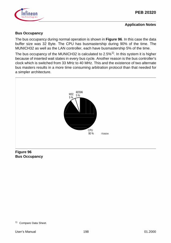
PEB 20320
Application Notes
Bus Occupancy
The bus occupancy during normal operation is shown in Figure 96. In this case the databuffer size was 32 Byte. The CPU has busmastership during 90% of the time. TheMUNICH32 as well as the LAN controller, each have busmastership 5% of the time.
The bus occupancy of the MUNICH32 is calculated to 2.5%1). In this system it is higherbecause of inserted wait states in every bus cycle. Another reason is the bus controller’sclock which is switched from 33 MHz to 40 MHz. This and the existence of two alternatebus masters results in a more time consuming arbitration protocol than that needed fora simpler architecture.
Figure 96Bus Occupancy
1) Compare Data Sheet.
ITD08294
i825965 %M32
5 %
CPU90 %
User’s Manual 198 01.2000

PEB 20320
Application Notes
MUNICH32 Polling
The influence of the polling can be illustrated by showing the bus occupancy ofMUNICH32 poll accesses only.
Figure 97Bus Occupancy During Polling
Here the MUNICH32 is polling 31 channels (= 31 × 2 read accesses during 125 µs).Every access is 5 clock cycles long, instead of the minimum length of 4 clock cycles. Thetime for the arbitration protocol needed during every access results in bus idle time.
ITD08295
Idle%10M32
17 %
CPU73 %
User’s Manual 199 01.2000

PEB 20320
Application Notes
Frame Processing
During normal operation the processing of a frame comprises three consecutive parts.During transmission from ISDN to LAN the frame is first processed from the MUNICH32,then from the CPU and finally from the LAN controller.
Figure 98Frame Processing
Though the CPU is never idle, its part on frame processing is that between theMUNICH32 and the LAN controller are active. The time to process one frame is theminimum delay required between frames during continuous transmission.
ITD08296
MUNICH32
CPU
i82596
t
Frame 1 Frame 2
User’s Manual 200 01.2000

PEB 20320
Application Notes
5.2.5 Final Remarks
This application note shows a design example for the MUNICH32 (PEB 20320). Thoughthe design example is of reduced complexity it gives an idea of how to use theMUNICH32 in a system. The MUNICH32 is integrated in a 68040 processor system inconjunction with one more alternate bus master.
To achieve higher data rates the time to process the frames should be minimized. Thisincludes minimization of bus idle time. The bus arbitration still has big improvementpotential because of its modular structure. Additionally the existence of the alternate busmasters results in clocking the bus controller with two different frequencies. This alsoresults in increased idle time for the bus should therefore be modified. Furthermoreframe processing could be shortened by eliminating the wait states in every bus cycle.
The influence of MUNICH32 poll accesses is extremely high in this example, because ofthe bus arbitration architecture and the system architecture with one bus controller for allbus masters. But anyway it should always kept in mind, that the bus occupancy duringpolling is higher than during transmission. During transmission it decreases rapidly.
No upper layer software is realized in this example so far. For ‘real life’ routing layer 2and 3 software module(s) have to be integrated.
User’s Manual 201 01.2000

PEB 20320
Application Notes
Figure 99Integration of Upper Layer Software
ITS08297
Message Descr
MUNICH32RC Descr
TX DescrMUNICH32 MUNICH32
DDM DDMLAN Controller
Message Descr
LAN ControllerTX Descr
LAN ControllerRC Descr
ISDN Route Frame
LAN Route Frame
MROUTE Module
Upper LayerSoftwareSoftware
Upper Layer
User’s Manual 202 01.2000
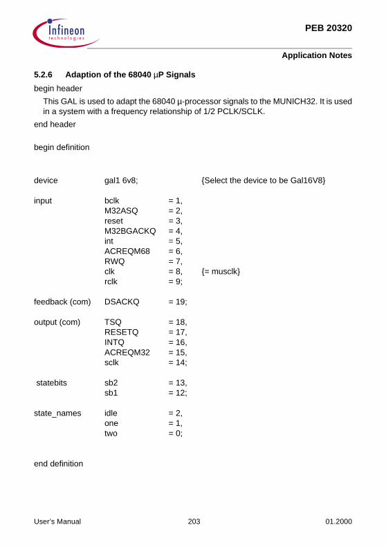
PEB 20320
Application Notes
5.2.6 Adaption of the 68040 µP Signals
begin header
This GAL is used to adapt the 68040 µ-processor signals to the MUNICH32. It is usedin a system with a frequency relationship of 1/2 PCLK/SCLK.
end header
begin definition
device gal1 6v8; Select the device to be Gal16V8
input bclk = 1,M32ASQ = 2,reset = 3,M32BGACKQ = 4,int = 5,ACREQM68 = 6,RWQ = 7,clk = 8, = musclkrclk = 9;
feedback (com) DSACKQ = 19;
output (com) TSQ = 18,RESETQ = 17,INTQ = 16,ACREQM32 = 15,sclk = 14;
statebits sb2 = 13,sb1 = 12;
state_names idle = 2,one = 1,two = 0;
end definition
User’s Manual 203 01.2000

PEB 20320
Application Notes
begin equationsTSQ.OE = /M32BGACKQ;TSQ = /(/M32ASQ × DSACKQ);RESETQ = /reset;INTQ = int;ACREQM32 = /(/ACREQM68 × reset × /RWQ);sclk = (/reset × rclk) + (reset × /clk);
end equations
begin state_diagram tktadaptor (sb2, sb1)
state all:if (/reset + M32ASQ) then idlewith DSACKQ = 1;endwith;
state idle:DSACKQ = 1;if (/M32ASQ × reset) then one else idle;
state one:DSACKQ = 1;go to two;
state two:DSACKQ = 0;if M32ASQ then idle else two;
end state_diagram
User’s Manual 204 01.2000

PEB 20320
Application Notes
5.2.7 Schematics
Figure 100
ITS08298
LAN Interface
SERINT.SCH LAN_CONT.SCH
MUBGQMUBGOQMUBGACKQMUBRQ
BGQBGACKQBRQ
ISDN
EASY320.SCH
SER_INT
MUBGQMUBGOQMUBGACKQMUBRQ
BGQBGACKQBRQ
Ctrl
A
D
Ctrl
A
D
User’s Manual 205 01.2000
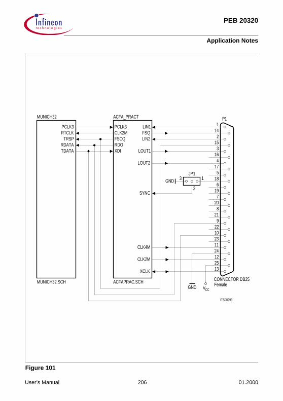
PEB 20320
Application Notes
Figure 101
ITS08299
1P
5174
163
152
141
186
197
208
219
1325122411231022
GND 13
2
JP1
GND CCV
LIN1FSQLIN2
LOUT1
LOUT2
SYNC
CLK4M
CLK2M
XCLK
ACFA_PRACT
ACFAPRAC.SCH
MUNICH32
MUNICH32.SCH
PCLK3RTCLK
TRSP
PCLK3CLK2MFSCQ
XDIRDO
TDATARDATA
CONNECTOR DB25Female
User’s Manual 206 01.2000

PEB 20320
Application Notes
Figure 102
ITS08300
J1A32 A32
31 31
30 30
29 29
28 28
27 27
26 26
25 25
24 24
23 23
22 22
21 21
20 20
19 19
18 18
17 17
16 16
15 15
14 14
13 13
12 12
11 11
10 10
9 98 8
7 7
6 6
5 5
4 4
3 3
2 2
1 1
VG96
AAAAAAAAAAAAAAAAAAAAAAAAAAAAA2
3456789
11
19
21
29
31
10
12131415161718
20
22232425262728
30 30
28272625242322
20
18171615141312
10
31
29
21
19
11
98765432
VG96
651
662
673
684
695
706
717
728
739
7410
7511
7612
7713
7814
7915
8016
8117
8218
8319
8420
8521
8622
8723
8824
8925
9026
9127
9228
9329
9430
953132 D96
J1C
DDDDDDDDDDDDDDDDDDDDDDDDDDDDDDD0
1
U1
MUNICH32
100 BE01BE96
2BE94
3BE91102 AA2
3A A1074A A1095A A1146A A1167A A1208A A1229A A12610A A12811A A13312A A13513A A13914A A14315A A14716A A14917A A15418A A15619A A16020A A221A A622A A823A A1324A A1525A A1926A A2127A A2628A A2829A A3330A A3531A A39
32 292927 282825 272720 262618 252514 242412 23237 22225 21211 2020
159 1919155 1818153 1717148 1616146 1515142 1414138 1313134 1212132 1111127 1010125 99121 88119 77115 66113 55108 44106 33101 2299 11
0D 0D95DDDDDDDDDDDDDDDDDDDDDDDDDDDDDDD
3031 38
34
DDDDDDDDDDDDDDDDDDDDDDDDDDDDDDD31
30
90 W,R/R,W85 ADS/AS86 DS75 READY/DSACK76 BERR74 B82 HOLD/BR79 HLDA/BG81 PM80 HLDAO/BGO66 AR40 INT/INT
16
MUINTQCRSTQ
ADDWSQ
PCSQ5WRQBGACKQM32BGQLOCKQBGQTSQBCLKBBQ
VG96
331
342
353
364
375
386
397
408
419
4210
4311
4412
4513
4614
4715
4816
4917
5018
5119
5220
5321
5422
5523
5624
5725
5826
5927
6028
6129
6230
633132 MUSCLK64
J1B
2JP1 2
GND
CCV
MUBGOQMUBGQ
RCLK 4445RSP
RDATA 4669TCLK
TSP 68
TSP 67
Ωk4.7
1RP
8 9
7 10
6 11
5 12
4 13
3 14
2 15
161CCV
MUBGACKQ
U7
OE 11MUSCLKCLK
8 9Ι7Ι 8
7Ι 65Ι 6
4Ι 5
3Ι 43Ι 2
1Ι 2
GAL16V8
12 O87O13
14 O6
SCLK 61
15 O516 O417 O360RESET18 O2
O119DSACKQ
563JTESTJTEST 2 55JTEST 1 54JTEST 0 53
19 1O2O183O174O165O156O14
13 O78O12
GAL16V8
2Ι 12Ι 3
4Ι 3
5Ι 4
6Ι 56Ι 7
8Ι 7Ι 98
CLK
11OE
U8 GND
BCLK
M32BGQ
MUBRQCCV1R
3.3 kΩ
BRQBGACKQ
M32BGQ
PCLK3TDATARDATATRSPRTCLK
GND
CCV1C
100 nF nF100C2
nF100C3
nF100C4
nF100C5
nF100C6
nF100C7
nF100C8
nF100C9
nF100C10
nF100C11
nF100C12
nF100C13
nF100C14
ASQCRSTQMUBGACKQINTPCSQ5RWQ
TSQMUINTQ
GND
CRSTQBBQLOCKQBRQBGACKQ
3130292827262524232221201918171615141312111098765432
PCLK3
BGQ
0CI123
47484950
4 51
CICICICI
65TEST
73I/M
GND
User’s Manual 207 01.2000

PEB 20320
Application Notes
Figure 103
ITS08301
VG96J2A
11 2
2
33
44
55
66
77
88
99
1010
1111
1212
1313
1414
1515
1616
1717
1818
1919
2020
2121
2222
2323
2424
2525
2626
2727
2828
2929
3030
3131
3232
U3
CE46PCSQ222 RDFRDQ25FRDQ WR
5INTQ2 AINT36 ACKNL
2
U2A74HC04
R21 kΩ
CCV
D1LED Red
1
3JP
223311
Ωk4.73R
CCV
18 AADR01ADR A192ADR A203ADR A21
0123
274
34
338
RDOCOSRDOXDI
ROIDXOIDRSIGM39
XSIGM40
RCHPY6
VCC
R410 kΩ
37 XCHPYAD0 9 D0
1D101
2D112
3D123
4D134
5D145
6D156
7D167
ACFA
CLK1
GND
1Ι2
2Ι3
3Ι4
4Ι5
5Ι6
6Ι7
7Ι8
8Ι9
OE11
U10
GAL16V8
1O 1918O 217O316O415O 514O613O712O 8
LOOPRSTQRDOAD0AD1AD2AD4AD5
PCSQ2G0G1G2G4G5GXDIG6
ADR
0AD
R1
ADR
2AD
R3
3031
3637
3839404
322829
1 32
JP4
FSCCLK2MCLK4MQXCLKCLK2MQ
XTOM 3
XTOP 44
XDOM 43
XDOP 42
RDIM 31
RDIP 30
XRCLK 41
RRCLK 29
SCLK 28
732
35
RFSPSYP
RES
D21N4148
U2B
GreenLEDD3
3 4
C1547 nF
GND
6RkΩ1
74HC041 ΩM
R5
CCV GND
GXDICOS
7
ADADADADADADAD
XDI
User’s Manual 208 01.2000

PEB 20320
Application Notes
Figure 104
ITS08302
PCSQ2G0G1G2G4G5GXDIG6
4AD
3AD
1AD
0AD
9695949392919089888786858483828180797877767574737271706968676665
J2CVG96
AD5
AD6
AD7
6 FSC7 FSC
XDIN3031 XDIP
RDOP3637 RDON
RCLK3839 CLK2M40 CLK2M4 CLK4M5 CLK4M
16 CLK12M15 CLK16M32 XCLK28 XTIN29 XTIP
U4
FSCQFSCCLK2MCLK4MQXCLKCLK2MQ
PRACT
pF1217C C18
12 pF
X2
16C C19
23CC20pF10
22CC2110 pF
33 9 10 12 13 43 11142632717
CS XTAL
XTAL
XTAL
XTAL
4 3 2 1
LSLSLRLLMO
DE
JATT
SYNC
LS8
02 1
2.2 ΩkR
VCC
LPCOSJATTMODE
4AD
2AD1AD0AD
WRQPCSQ3RSTQ
8O 127O 136O 145O 154O 163O 172O 18
19O1
GAL16V8
U9
11 OE
9 Ι 8
8 Ι 7
7 Ι 6
6 Ι 5
5 Ι 4
4 Ι 3
3 Ι 2
2 Ι 1
GND
1 CLK
3AD
PCLK3
LOOP
2.2 kΩ
R15
CCV
33 34 35 36 37 38 39 40 41 42 43 44 45 46 47 48 49 50 51 52 53 54 55 56 57 58 59 60 61 62 63 64
GND CCV
VG96J2B
RSTQ
INTQ
2
PCSQ
4PC
SQ3
PCSQ
2
WRQ
FRDQ
XDIRDOSYNCCLK2MCLK2MQCLK4MQFSCFSCQXCLKCLK33_CON
GND
35 41 23 22
SSD
V V SSR
SSX
VV SSX
47 nFC24
DDX
V V DDX
DDR
VV DDD
18194234
DD2
V1
25Cµ47
CCV
RkΩ60
11
1160 ΩkR
nF10026CCCV
GND
GNDCCV
D10 D11
VCCGND
8
15 Ωk
R
R
kΩ15
7
D8 D9
D5D4
GND CCV
D6
VCCGND
D7
12XL
XL
RLRL 2
1
2024442
3
8
6
5
5
6
8
3 U6
U5 9
1 Ωk
R
R
kΩ1
14
F6SO5K130
GND
1
2
1
2
LOUT1
LIN1
2
1
2
1
GND
SO5K130F5
13
1 Ωk
R
R
kΩ1
12
LOUT2
LIN2
F1A81_C90X
F3A81_C90X
A81_C90XF2
A81_C90XF4
ZKB_402/512
ZKB_402/512
nF10031CC30
100 nFnF10029C
nF10028C
GND
CCV
G01
G2
G
6G G G
54
JATT
SYNC
MO
DE
3231302928272625242322212019181716151413121110987654321 1 2 3 4 5 6 7 8 9 10 11 12 13 14 15 16 17 18 19 20 21 22 23 24 25 26 27 28 29 30 31 32
PCLK3
AD2
F
16 MHz
MHz12X1
GND
1
10
10
1
User’s Manual 209 01.2000
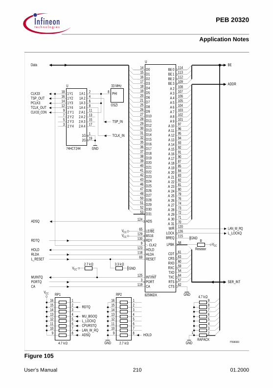
PEB 20320
Application Notes
Figure 105
ITS08303
14 D01D15
2D16
3D17
4D18
5D19
6D20
7D21
8D25
9D26
10D27
11D28
12D29
13D30
14D31
15D32
16D35
17D36
18D37
19D38
20D39
21D40
22D41
23D42
24D43
25D46
26D47
27D48
28D50
29D51
30D52
31D53
1140BEBE 1 113
BE 2 112
BE 3 109
A 10823A 107
4A 106
5A 105
6A 104
7A 103
8A 102
9A 101
10A 97
11A 96
12A 95
13A 94
14A 93
15A 92
16A 91
17A 90
18A 87
19A 85
20A 84
21A 83
22A 82
23A 81
24A 80
25A 79
26A 76
27A 74
28A 73
29A 72
30A 71
31A 70
U
18 1116
114
112
29
27
25
23 YYYYYYYY1
2341234
1A11A 21A 31A 42 A 12 A 22 A 32 A 4
U
CLK33TSP_OUTPCLK3TCLK_OUTCLK33_CON
74HCT244
1G2G 19
1
171513
PHI8
33 MHz
GND
TCLK_IN
TSP_IN
OSZI118642
Data
CCV
124
65129130
9123118
69
ADS
LE/BEBSRDY
HOLDHLDARESET
CLK2
16
3 PORT
125 INT/INT
119 CA
3.3 kΩGNDVCC
2.7 kΩ
82596DX
RDTQ
ADSQ
HOLDRLDAL_RESET
PORTQCA
MUINTQ
GND
57RTSCTS
TXC 64TXD 54RXC 59RXD 60CRS 63CDT 61
62
VCC
115BREQ GND
Resistor
R
126120
58
LOCKW/R
LPBK
16 121531441351261171089
RP1
4.7 kΩ
RDTQ
MU_BGOQL_LOCKQCPURSTQLAN_W_RQADSQ HOLD
Ωk2.7
2RP
9 810 711 612 513 414 315 2
116
GND GND
1 23456789
4.7 Ωk
SER_INT
L_LOCKQLAN_W_RQ
ADDR
BE
RAPACK
VCC
CCV
User’s Manual 210 01.2000

PEB 20320
Application Notes
Figure 106
ITS08310
8O 127O 136O 145O 154O 163O 172O 18
19O1
GAL16V8A
RESET
11 OE
9 Ι 8
8 Ι 7
7 Ι 6
6 Ι 5
5 Ι 4
4 Ι 3
3 Ι 2
2 Ι 1
GND
1 CLK
MUCLK
CPURSTQ
L_RESET
PORTQ
CPURSTQ
MUCLK
CLK1
GND
1Ι2
2Ι3
3Ι4
4Ι5
5Ι6
6Ι7
7Ι8
8Ι9
OE11
Port
GAL16V8A
1O 1918O 217O316O415O 514O613O712O 8
CA
M32_ARQ
DTOEQLAN_CSQR_WQM32_ARQ
CLK33
GND
CLK33
HLDAIN
TSQR_WQ
8O 127O 136O 145O 154O 163O 172O 18
19O1
GAL16V8A
Signal
11 OE
9 Ι 8
8 Ι 7
7 Ι 6
6 Ι 5
5 Ι 4
4 Ι 3
3 Ι 2
2 Ι 1
GND
1 CLK
TAQRDYQ
ADSQLAN_W_RQ
HOLDMU_BRQ
BRQML_BGQ
CLK1
GND
1Ι2
2Ι3
3Ι4
4Ι5
5Ι6
6Ι7
7Ι8
8Ι9
OE11
Arbiter
GAL16V8A
1O 1918O 217O316O415O 514O613O712O 8
BGACKQHLDAIN
MUCLK
CLK33
2
MU_BGACKQ
CPURSTQ
MU_BGQ
M32_CSQ
A4
ML_BGQMU_BGACKQ
LAN_CSQSIZ1
8O 127O 136O 145O 154O 163O 172O 18
19O1
GAL16V8A
Address
11 OE
9 Ι 8
8 Ι 7
7 Ι 6
6 Ι 5
5 Ι 4
4 Ι 3
3 Ι 2
2 Ι 1
GND
1 CLK
A0PCSQ5 A1
SIZ0
BEBEQ0BEQ1BEQ2BEQ3
User’s Manual 211 01.2000

PEB 20320
Application Notes
Figure 107
ITS08311
J1C
65 D012 D66
3 D67
4 D68
5 D69
6 D70
7 D71
8 D72
9 D73
10 D74
11 D75
12 D76
13 D77
14 D78
15 D79
16 D80
17 D81
18 D82
19 D83
20 D84
21 D85
22 D86
23 D87
24 D88
25 D89
26 D90
27 D91
28 D92
29 D93
30 D94
31 D95
32 D96 31302928272625242322212019181716151413121110987654321
Data
VG96 VG96
Address
234567891011121314151617181920212223242526272829303132
31302928272625242322212019181716151413121110
987654321 0A
J1A
AAAAAAAAAAAAAAAAAAAAAAAAAAAAAAA
1
VG96
6432
6331
6230
6129
6028
5927
5826
5725
5624
5523
5422
5321
5220
5119
5018
4917
4816
4715
4614
4513
4412
4311
4210
419
408
397
386
375
364
353
3421 33
J1B
PCLK3DTOEQTAQ
MUINTQ0CPURSTQ
MUINTQ
GND
CCV
PCSQ5W_RQBGACKQML_BGQLOCKQBGQ_68TSQBCLKBBQ
MUCLK
User’s Manual 212 01.2000
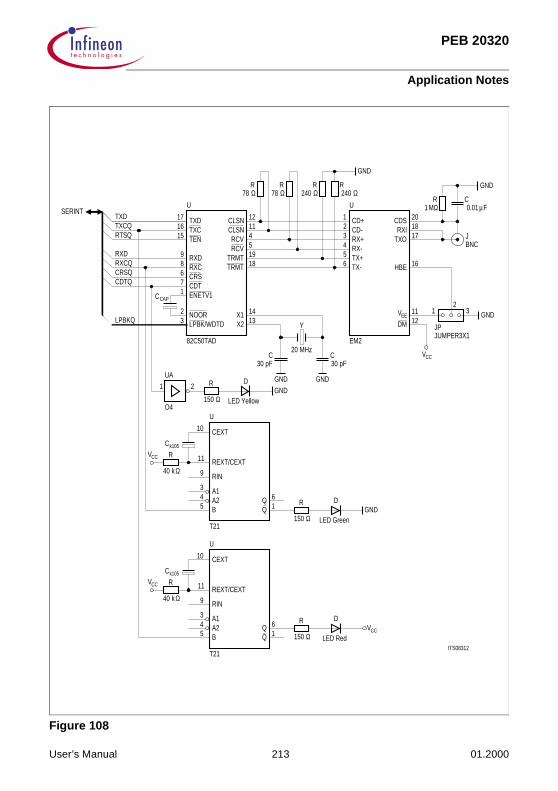
PEB 20320
Application Notes
Figure 108
ITS08312
17 TXDTXDTXCQ TXC16RTSQ TEN15
6 CRSCRSQ8 RXCRXCQ
RXD RXD9
CDTQ CDT7
ENETV11
2 NOOR
CAPC
LPBKQ 3 LPBK/WDTD
SERINTCLSN 12
11CLSNRCV 4
RCV 5
18TRMT
19TRMT
123
CD+CD-RX+
TX-TX+RX-
654
UU
82C50TAD EM2
GND GND
1314
Y
C30 pF pF30
C20 MHz
CDS 2018RXI17TXO
JP
1 32
GND
16
11
CCV
JUMPER3X1
HBE
DM
C0.01 µF1 MΩ
R
EEV
GND1 2
O4
R
150 Ω
D
LED Yellow
U
T21
5 B
4 A2A13
9 RIN
11 REXT/CEXTR
40 kΩ
10 CEXT
Ck105
CCV
X1X2
Q 61Q
LED Green
D
D
LED RedQ
61
Q
k105C
CEXT10
RREXT/CEXT11
RIN9
3 A1A24
B5
T21
U
R
150 Ω
R
150 Ω
UA
CCV
40 kΩ
VCC
GND
12
GND
GND
JBNC
RΩ78 78 Ω
R240 Ω
R240 ΩR
User’s Manual 213 01.2000

PEB 20320
Application Notes
5.3 Memory Bus Occupancy for a Single MUNICH32
The MUNICH32 may be used in different system architectures depending mainly on howthe data buffers are shared between the interacting bus masters. In the following thememory bus occupancy is calculated for a system, where the MUNICH32 is directlycoupled with a 32-bit CPU (compatible to either Motorola 68020 or Intel 386) sharing onecommon local CPU bus and translated via an appropriate system bus controller sharingthe system memory as well. This example system looks very similar to the one depictedin the Figure 7 and Figure 9 of Chapter 1. In this case it is easier to estimate thebehavior of the complete system.
In addition to that, the following assumptions are made about the communicationparameters:
– HDLC operating mode– the MUNICH is clocked with SCLK = 16 MHz– the bus arbitration time is estimated to be about 4 extra clock cycles (SCLK) for every
10 MUNICH32 memory accesses (typical is 10 to 16)– the data buffer size allocated in the data buffer pool is 32 bytes for transmit and
receive descriptors– a full duplex connection with up to 32 × 64 Kbit/s channels and heavy traffic load
(shared flags)– the data size per HDLC frame is defined to be without the shared flag and the two CRC
bytes– when the data size exceeds 32 bytes, more than one descriptor is needed for a single
frame– an interrupt information is generated for every descriptor.
The MUNICH32 needs the following 32-bit memory accesses (read or write):
Receive: read descriptor → 3write current descriptor address → 1write status → 1write interrupt → 1write data (size) → accesses size
1 11 21 31 42 5: :
User’s Manual 214 01.2000

PEB 20320
Application Notes
Transmit: read descriptor → 3write current descriptor address → 1write interrupt → 1read data (size) → accesses size
1 11 21 31 42 5: :
The accumulated access time for a single MUNICH32 channel, depending on the actualframe size, is then related to the serial transfer time on a PCM system:(3 + size) × 125 µs.
The following two diagrams illustrate the overall results for two different ranges and theircorresponding resolution. As you can see, for frame size greater than 32 bytes the timeneeded for MUNICH32 memory accesses drops below 5%. That means in a simplecommunication subsystem (e.g. Primary Access Board) the CPU performance is alsoreduced by 5% only and it is therefore not necessary to use a complex multiport memoryapproach to reach a significant overall performance gain.
Figure 109Frame Size 1 to 512
ITD04696
0
1
5
10
15
20
25
32 64 96 128 160 192 224 256 288 320 352 384 416 448 480 512
%
Number of Data Bytes
Ch=32Ch=30Ch= 1
Memory Bus Occuppancy
User’s Manual 215 01.2000

PEB 20320
Application Notes
Figure 110Frame Size 1 to 32
0
1
5
10
15
20
25
%
29 30 31 3227 282 3 4 5 6 7 8 9 10 11 12 13 14 15 16 17 18 19 20 21 22 23 24 25 26
Memory Bus Occuppancy
Number of Data Bytes
ITD04697
Ch= 1Ch=30Ch=32
User’s Manual 216 01.2000

PEB 20320
Application Notes
5.3.1 Bus Occupancy Calculations
As described in the previous section, the MUNICH32 in a steady state conditionconsumes approximately 5% of the system bus bandwidth. Based on the conditionspreviously described, a set of equations can be used to describe the MUNICH32 systembus behavior. Other MUNICH32 systems can be evaluated using these equations. TheBus occupancy is defined as the ratio of the time required for memory accesses for thatdata to the time used to send the data. The two equations are defines as follows:
Time used for memory accesses:
= Number of received bits plus transmitted bits multiplied by the time required totransfer this
information to/from memory.= ([6 + (1 + m)] × rc) + (5 + (1 + m)] × tc) × (1 + 1/ba) × NC × sclk
6 for receive descriptor access5 for transmit descriptor access(1 + m) for data access where m is the largest integer smaller (n – 1)/4(n is the number of transmitted data bytes).rc is the number of receive channels.tc is the number of transmit channels.(1 + 1/ba) is the bus arbitration timesclk is the system clock (61 ns for 16.384 MHz)NC is the number of memory clocks per bus operation (0ws = 4, 1WS = 5, etc.).
Time used to send the data is the number of transmitted bits per time slot multiplied bythe frame time:
= ((4 + n) × 8/abtc) × 125 µs4 because shared flags are not used + 2 byte CRCn is the number of octets to transmitabtc = assigned bits to channele.g. a channel with one time slot of 1 bit would require 8/1 = 8 time slots totransmit a single octet.
From the previous example, the variables are assigned the following values:
Variable n m rc tc (1 + 1/ba) sclk NC abtc
Value 32 bytes 7 32 32 1.1 61 ns 4 8
User’s Manual 217 01.2000

PEB 20320
Application Notes
Applying these values to the equations yields the following:
Time used to access memory= ([6 + (1 + 7)] × 32) + ([5 + (1 + 7)] × 32) × (1.1) × 4 × 61 ns = (14 × 32) + (13 × 32) × 1.1 × 244 ns = 864 × 268.4 ns = 231.9 µs.
Time used to send data= ((4 + 32) × 8/8) × 125 µs.= 36 × 125 µs.= 4500 µs.
Bus occupancy = 231.9 µs/4500 µs = 5.1%
When the packet size is much larger (256 bytes or larger), the bus occupancy decreasesto less than 4%. Conversely, sending very small frames (4 bytes), causes busoccupancy to increase to over 11%. This is primarily due to the increased descriptorprocessing per packet.
5.3.2 Bus Occupancy for Idle Tx Channels
The previous discussion shows bus occupancy to be very low, even when a MUNICH32is processing 32 channels of receive and transmit data. There is another systemconsideration of bus occupancy that must be examined. When a MUNICH32 channelhas no data required for transmit, the channel must be temporarily (or permanently)stopped. There are several methods that may be used to stop the transmission.
1. The first method involves executing a channel command with TH = 1 (reactivation ofthe channel requires a new channel command with TH = 0). This method places thetransmit channel on hold and prevents any further accesses of the memory for thischannel.
2. A second method is based on statistical knowledge of the frequency of transmittedframes. If frames are transmitted without shared flags and if the average number ofinterframe time fill characters can be determined, the MUNICH32 can be programmedto suppress poll sequences. By setting FNUM in the Tx descriptor to a value (n)greater than 0, the MUNICH32 will transmit n + 1 idle characters after the end of thecurrent frame. During this period of interframe time fill, the MUNICH32 will not poll theTx descriptor. As an example, if it is determined that 5 idle characters typically occurbetween frames, FNUM can be set to 4. At the end of the current frame, 5 idlecharacters will be transmitted (625 µs. on a DS0 channel) before the next frame istransmitted and no polls of the Tx descriptor will occur during that time.
User’s Manual 218 01.2000
PEB 20320
Application Notes
3. The final method is to set the HOLD bit in the Tx descriptor. When the HOLD bit in theTx descriptor is set, the MUNICH32 checks the status of the this bit for each time slotassigned to this channel. In this way, if the bit has been cleared, the MUNICH32 willimmediately resume transmission. Although this method is simpler (in concept) for thesoftware design, it causes the MUNICH32 to consume higher than normal busbandwidth. For this reason, this is the least desirable of the three methods. In theprevious example discussed, if all 32 channels were holding on the Tx descriptors,bus occupancy might rise as high as 17%. The reason bus occupancy rises thisdramatically is due to the bus access once per time slot rather than once every fourtime slots (typical).
User’s Manual 219 01.2000

PEB 20320
Application Hints
6 Application Hints
6.1 Frequency Adaption in an Intel 368 Common Bus System
If you use the i386 as host processor with the MUNICH32 in a common bus system youhave to adapt the different frequencies of the devices. The MUNICH32 works e.g. witha fixed frequency of 16.384 MHz in CEPT 32 channel PCM highway format. The i386works with frequencies from 16 up to more than 50 MHz. If you compare the timingdiagrams you will see that a few glue logic is necessary to adapt the MUNICH32 to thei386 timing.
A possible adaption of the different frequencies is described below. For an example weuse an i386 with a frequency of 16.384 MHz. The MUNICH32 is configured in the CEPT32 channel PCM highway format with a SCLK of 16.384 MHz. The SCLK signal is buildby dividing the 32.768 MHz CLK2 signal of the i386. That means that both clocks aresynchronous. This is not necessary in general but selected in our example. The buscontroller generates e.g. one wait state for the memory access. The falling edge of theADS signal marks the beginning of a bus cycle which is completed with the sampledREADY signal. A general bus controller should not see a difference between the two busmasters, so we have to delay the falling edge of the MUNICH32 ADS signal to thatmoment as the i386 would generate its ADS to get the READY signal at the same time.In the picture below you can see the relationship and the adaption of both timings asspecified in our example. A second picture shows the adaption in an i386 24.576 MHzsystem. Again the clocks are synchronous.
User’s Manual 220 01.2000

PEB 20320
Application Hints
Figure 111
ITD04556
SCLK
ADS
READY
CLK
CLK2
ADS
READY
S1 S2
MUNICH32SCLK=16.384 MHz
T1
Delay
i386, 16.384=>CLK2=2xSCLK
MHz
T1 T2T2 T1
User’s Manual 221 01.2000

PEB 20320
Application Hints
Figure 112
ITD04557
SCLK
ADS
READY
CLK
CLK2
ADS
READY
S1 S2
MUNICH32SCLK=16.384 MHz
T1
Delay
i386, 24.576=>CLK2=3xSCLK
MHz
T1 T1 T1 T2 T2 T1
User’s Manual 222 01.2000
PEB 20320
Application Hints
6.2 MUNICH32 Memory Space Requirement
Implementation independent:
– Start Address 4 byte– Control & Configuration Section 908 byte– Tx Descriptor Size 12 byte– Rc Descriptor Size 16 byte
Implementation dependent:
– Interrupt Queue Size 64 byte < Interrupt Queue Size < 16384 byte– Data Buffer Size Data Buffer Size– Allocation of Tx and Rc descriptors per channel
In general the memory space requirement may be calculated the following way:
Start Address+ Size of Control & Configuration Section+ Interrupt Queue Size+ number of channels × [number of Tx Descriptors × (Tx Descriptor Size + Data Buffer Size)] +number of channels × [number of Rc Descriptors × (Rc Descriptor Size + Data Buffer Size)] –––––––––––––––––––––––––––––––––––––––––––––= Total MUNICH32 Memory Space Requirement
Example:
The MUNICH32 is used in a 31 channel ISDN Primary Access application, that meansthat 31 full duplex channels are active. The LAPD protocol is implemented. In this casea window size of 7 is specified, that means that 7 Rc Descriptors and in transmit direction7 Tx Descriptors must be available for each channel. The Data Buffer Size is set to 260byte according to the LAPD specification.
Summary:
– 31 channels;– Interrupt Queue Size = 1024 byte;– 7 Tx and 7 Rc Descriptors;– Data Buffer Size = 260 byte;
In our example a memory space of 120 kbytes is required.
User’s Manual 223 01.2000

PEB 20320
Application Hints
6.3 Serial Interface to different PCM Systems
The serial interface of the MUNICH32 is very general and comprises standard clock,PCM frame synchronization and data signals, which are independent for both directions.The following description explains typical applications integrating the MUNICH32 into2.048 Mbps PCM systems, like SIEMENS System Interface for Primary Access and theMITEL ST BUS. In these systems the receive and transmit clocks are identical. Thegeneral timing is shown in Figure 113 (see also Chapter 2.1).
Figure 113
The RSP pulse is shifted by one clock period against the TSP pulse. The main task usingthis timing for different PCM systems is to adapt the TSP and RSP pulses appropriately,as described below.
6.3.1 MUNICH32 for SIEMENS Primary Access Interface
The SIEMENS devices for the Primary Access Interface is the Frame and Line InterfaceComponent (FALC54). This device can directly be connected to the MUNICH32 withoutany additional glue logic. In combination with the MUNICH32 this application is the mosteffective way to build a powerful and flexible Primary Access Interface, especiallysupporting different combined B channel paths over long distances (LAN-WANInternetworking). The following block diagram illustrates how easy it is to integrate theMUNICH32 into a Primary Access application based on SIEMENS devices.
ITD04694
Time-Slot 0
Time-Slot 0
RCLK=TCLK
TSP
RSP
TDATA
RDATA
User’s Manual 224 01.2000

PEB 20320
Application Hints
Figure 114
The adaption of the TSP and RSP pulses is solved by means of shifting the receive dataand transmit data in the FALC54 device appropriately. In this case the TSP and RSPsynchronization pulses are also identical. The FALC54 device contains special registersto control the bit shift of the serial bit streams at the system interface (see FALC54 DataSheet). With the following register programming the bit shift selected is T = 509 for theMUNICH32 transmit data and T = – 1 for the receive data respectively. Theprogramming is as follows:
XDI: XC1.XTO = 3DH => X = 494 => T = 509XC0.XCO = 06H
RDO: RC1.RTO = 00H => X = 5 => T = – 1 RC0.RCO = 05H
ITS07370
TCLKTSP
TDATA
RDATARSP
RCLK
XDI
RDO
CLK8MCLKX
MUNICH32PEB 20320 2254PEB
FALC54SCLKX
SYPXQ
SCLKR
SYPRQ
FSCFSCQ
User’s Manual 225 01.2000

PEB 20320
Application Hints
The timing in principle is depicted in the following diagram. Without all details of a typicalelectrical timing it illustrates how the different signals from MUNICH32, and FALC54 aremapped in such a Primary Access system.
Figure 115
ITD08282
FSC=TSP=RSP
CLKX=RCLK=TCLK
TDATA
=XDI
RDATA
=RDO
(T=509)
(T=-1)
= : Invalid area
Channel 0, Bit 0 (Least Significant Bit):=
User’s Manual 226 01.2000

PEB 20320
Application Hints
6.3.2 MUNICH32 in Systems with MITEL ST BUS
A few more effort is necessary to integrate the MUNICH32 into a ST BUS system fromMITEL. The basic assumption made here is that the clock master is the ST BUS system.That means all signals derived from the ST BUS need to be adapted to match theMUNICH32 timing requirements. First of all the clock signal C2 must be inverted beforeit can be used as the MUNICH32 clocks (TCLK = RCLK = C2). The next step is thegeneration of the TSP and RSP pulses out of the F0 signal, which is the ST BUS framesynchronization signal. The RSP pulse can be derived from the F0 signal by means of asimple D-Flip-Flop clocked with C2, as depicted in the following Figure 116. Due to thenecessary phase relationship between the serial data streams and their correspondingTSP, RSP and F0 pulses, the effort to generate the TSP pulse is much higher than forRSP.
Figure 116
ITS04692
TCLKTSP
TDATA
RDATARSP
RCLK
ST-BUS
STi
STo
MUNICH32PEB 20320
C2 F0
&Q
Q D
RES
8-BitCounter
DQ
Q
System Clock Adaption
Decode’254’
User’s Manual 227 01.2000

PEB 20320
Application Hints
The TSP pulse must be derived from the F0 signal with a phase shift by 255 clock cyclesto be at the right position. The corresponding timing is illustrated in the following diagram.
Figure 117
ITD04693
C2
F0
TSP
RCLK=TCLK=C2
TDATA
=STi
RDATA
=STo
= : Invalid area
Channel 0, Bit 0 (Least Significant Bit):=
Derived from F0 and synchronized by means of C2*)
RSP
*)
*)
User’s Manual 228 01.2000

PEB 20320
Electrical Characteristics
7 Electrical Characteristics
Note: All specifications are for V3.4 unless otherwise specified. Version numbers areidentified in the Interrupt Information bits VN(3:1):these bits are ‘0000’ for version 1.1
‘0001’ for version 2.1‘0010’ for version 2.2‘0100’ for version 3.2‘0110’ for version 3.4
7.1 Absolute Maximum Ratings
Note: Stresses above those listed here may cause permanent damage to the device.Exposure to absolute maximum rating conditions for extended periods may affectdevice reliability.
Table 12
Parameter Symbol Limit Values Unit
min. max.
Ambient temperature under bias: PEBPEF
TA
TA
0– 40
7085
°C
Storage temperature Tstg – 65 125 °CVoltage at any pin with respect to ground VS – 0.4 VDD + 0.4 V
User’s Manual 229 01.2000

PEB 20320
Electrical Characteristics
7.2 DC Characteristics
Note: The listed characteristics are ensured over the operating range of the integratedcircuit. Typical characteristics specify mean values expected over the productionspread. If not otherwise specified, typical characteristics apply at TA = 25 °C andthe given supply voltage.
Table 13TA = 0 to + 70 °C; VDD = 5 V ± 5%, VSS = 0 V
Parameter Symbol Limit Values Unit Test Condition
min. max.
L-input voltage VIL – 0.4 0.8 V –
H-input voltage VIH 2.0 VDD + 0.4 V –
L-output voltage VQL – 0.45 V IQL = 7 mA(pin TDATA)IQL = 2 mA(all others)
H-output voltage
H-output voltage
VQH
VQH
VDD – 0.5
2.4
– V
V
IQH = – 2 mA(pin HOLD/BR)IQH = – 100 µA(all others)IQH = – 400 µA
Power supply current
operational ICC – < 100 mA VDD = 5 Vinputs at 0 V/VDD,no outputs loads
power down (no clocks)
ICC – < 2 mA
Input leakage currentOutput leakage current
ILI
ILQ
– 10 µA 0 V < VIN < VDD to 0 V0 V < VOUT < VDD to 0 V
User’s Manual 230 01.2000

PEB 20320
Electrical Characteristics
7.3 Capacitances
7.4 AC Characteristics
TA = 0 to + 70 °C; VDD = 5 V ± 5%
Inputs are driven to 2.4 V for a logical ‘1’ and to 0.4 V for a logical ‘0’. Timingmeasurements are made at 2.0 V for a logical ‘1’ and at 0.8 V for a logical ‘0’.
The AC testing input/output waveforms are shown below.
Figure 118Input/Output Waveform for AC Tests
Table 14TA = 25 °C; VDD = 5 V ± 5%, VSS = 0 V
Parameter Symbol Limit Values Unit Test Condition
min. max.
Input capacitance CIN 5 10 pF –
Output capacitance COUT 8 15 pF –
I/O-capacitance CIO 10 20 pF –
ITS00621
= 150LoadCTestUnderDevice
0.45
2.42.0
0.80.8
2.0
Test Points
pF
User’s Manual 231 01.2000

PEB 20320
Electrical Characteristics
7.5 Microprocessor Interface Intel Bus Mode
Figure 119Timing Diagram Intel Bus Mode
ITD03510
1
SCLK
A31-A2
BE(3:0),
ADS
READY
2
D31-D0
3 3 4
5
8
(read cycle)
(write cycle)
D31-D0
BERR
S1 S2 S1
109
76
PCHK
[DP(3:0)]
[DP(3:0)]
11 11
User’s Manual 232 01.2000

PEB 20320
Electrical Characteristics
Figure 120Bus Arbitration Timing Diagram Intel Bus Mode
Intel Bus Timing
Table 15
No. Parameter Limit Values Unit
min. max.
1 Address, valid delay – 20 ns
2 BE, INT, W/R valid delay – 20 ns
3 ADS valid delay – 20 ns
4 READY setup time 10 – ns
5 READY hold time 5 – ns
6 BERR setup time 10 – ns
7 BERR hold time 5 – ns
8 Data valid delay (write) – 35 ns
9 Data setup time (read) 5 – ns
10 Data hold time (read) 8 – ns
ITD03511
12 12
13 13
14 15
16 17High Z High Z
SCLK
HOLD
HLDAO
HLDA
MicroprocessorInterface
11
PCHK
User’s Manual 233 01.2000

PEB 20320
Electrical Characteristics
11 Parity check valid delay – 50 ns
12 HOLD valid delay – 20 ns
13 HLDAO valid delay – 20 ns
14 HLDA setup time 10 – ns
15 HLDA hold time 10 – ns
16 Microprocessor Interface (MI) driven after HLDA set
2 SCLK cycles – –
17 MI tristated after bus accesses – 40 ns
Table 15
No. Parameter Limit Values Unit
min. max.
User’s Manual 234 01.2000

PEB 20320
Electrical Characteristics
7.6 Microprocessor Interface Motorola Bus Mode
Figure 121Timing Diagram Motorola Bus Mode
ITD03513
18
20
SCLK
A31-A2
INT, BE (3:0), R/W
AS
DSACK
D31-D0
1921 21
2322
24 25
(read cycle)
(write cycle)D31-D0
BERR
DS
T1 T2 T3 T4 T1
28
29
19
26
27
User’s Manual 235 01.2000

PEB 20320
Electrical Characteristics
Figure 122Bus Arbitration Timing Motorola Bus Mode
Motorola Bus Timing
Table 16
No. Parameter Limit Values Unit
min. max.
18 Address, BE, INT, R/W valid delay – 20 ns
19 AS, DS asserted after clock low – 20 ns
20 AS, DS negated after clock low – 20 ns
21 DSACK, BERR setup time to clock low 5 – ns
22 Data read setup time to clock low 5 – ns
23 Data read hold time to clock low 8 – ns
ITD03514
30
33
32
33
SCLK
BR
BG
BGACK
MicroprocessorInterface
30
31
35
36
34
BGO
SCLK
BR
BG
BGO
36 36
User’s Manual 236 01.2000

PEB 20320
Electrical Characteristics
24 Data write valid delay – 35 ns
25 Data write hold from clock high – 35 ns
26 Address valid to AS high 10 – ns
27 Data valid to DS low 10 – ns
28 DS high to data invalid 5 – ns
29 AS high to address invalid 10 – ns
30 BR valid delay – 25 ns
31 BG setup time to clock high 5 – ns
32 BG hold time after BGACK 10 – ns
33 BGACK valid delay – 25 ns
34 Microprocessor Interface driven after BGACK asserted
1 SCLK cycle
– –
35 Clock high to Microprocessor Interface tristated – 40 ns
36 BGO valid delay from clock high – 40 ns1) Newly specified for V2.1 and V2.2. Not specified in Data Sheet 08.93.
Table 16
No. Parameter Limit Values Unit
min. max.
User’s Manual 237 01.2000

PEB 20320
Electrical Characteristics
Serial Interface Timing
Figure 123
Table 17
No. Parameter Limit Values Unit
min. max.
37 Receive strobe guard time 10 – ns
38 Receive strobe setup 5 – ns
39 Receive strobe hold 5 – ns
40 Receive data setup 5 – ns
41 Receive data hold 5 – ns
RSP
RDATA
3937
42
38
43
4041
RCLK
TCLK
4847
50
45
49
44 46
TDATA
TSP
ITD03515
User’s Manual 238 01.2000

PEB 20320
Electrical Characteristics
Note: 1. The frequency on the serial line must be smaller or equal to1/8
th of the frequency on the µP bus for 1.536 MHz, 1.544 MHz, 2.048 MHz1/4
th of the frequency on the µP bus for 4.096 MHz.
2. For complete internal or complete external loop t42 and t49 must be greater orequal to 3 times t51.
Clock Input Timing
Figure 124Clock Timing
42 Receive clock high width 60 – ns
43 Receive clock low width 60 – ns
44 Transmit strobe guard time 20 – ns
45 Transmit strobe setup 5 – ns
46 Transmit strobe hold 5 – ns
47 Transmit data delay – 40 ns
48 Transmit clock to high impedance – 50 ns
49 Transmit clock high width 60 – ns
50 Transmit clock low width 60 – ns
Table 17 (cont’d)
No. Parameter Limit Values Unit
min. max.
5352
SCLK
ITD03516
51
User’s Manual 239 01.2000

PEB 20320
Electrical Characteristics
Note: If fT is the frequency of the clock TCLK, fR the frequency of the clock RCLK and fS
the frequency of the clock SCLK the equations7.996 × max (fT, fR) ≤ fS ≤ 16.667 MHZ for CEPT, T1, E1 PCM mode
and3.998 × max (fT, fR) ≤ fS ≤ 16.667 MHZ for 4.096 MHz PCM mode
describe the allowed range of frequencies for fS.
System Interface Timing
Figure 125
After power up a logical ‘1’ at the reset pin of the MUNICH V3.4 sets the device into areset state where the complete microprocessor bus interface is tristated and the internalreset sequence is started.
Table 18
No. Parameter Limit Values Unit
min. max
51 Cycle period 50 – ns
52 Clock low time 25 – ns
53 Clock high time 25 – ns
Table 19
No. Parameter Limit Values Unit
min. max.
55 Reset to first action request delay 12 SCLK cycles – –
56 AR# pulse width 2 SCLK cycles 5 SCLK cycles –
57 Reset pulse width 2 SCLK cycles – –
57
RESET
AR
56
ITT10668
55
after resetrequest ARfirst action
User’s Manual 240 01.2000
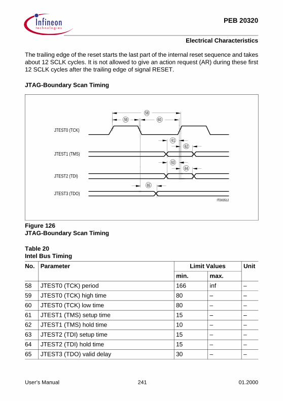
PEB 20320
Electrical Characteristics
The trailing edge of the reset starts the last part of the internal reset sequence and takesabout 12 SCLK cycles. It is not allowed to give an action request (AR) during these first12 SCLK cycles after the trailing edge of signal RESET.
JTAG-Boundary Scan Timing
Figure 126JTAG-Boundary Scan Timing
Table 20Intel Bus Timing
No. Parameter Limit Values Unit
min. max.
58 JTEST0 (TCK) period 166 inf –
59 JTEST0 (TCK) high time 80 – –
60 JTEST0 (TCK) low time 80 – –
61 JTEST1 (TMS) setup time 15 – –
62 JTEST1 (TMS) hold time 10 – –
63 JTEST2 (TDI) setup time 15 – –
64 JTEST2 (TDI) hold time 15 – –
65 JTEST3 (TDO) valid delay 30 – –
ITD03512
JTEST0 (TCK)
JTEST1 (TMS)
JTEST2 (TDI)
JTEST3 (TDO)
65
6261
59 60
6364
58
User’s Manual 241 01.2000

PEB 20320
Package Outlines
8 Package Outlines
GP
M05
247
P-MQFP-160-1(Plastic Metric Quad Flat Package)
Sorts of PackingPackage outlines for tubes, trays etc. are contained in our Data Book “Package Information”.
Dimensions in mmSMD = Surface Mounted Device
User’s Manual 242 01.2000

PEB 20320
Appendix
9 Appendix
9.1 Source Code Extract MUNICH32
The MUNICH32 code extract is taken from the low level device driver for the MUNICH32,which is written in ‘C’. This extract gives you a brief impression how a MUNICH32 devicedriver could be programmed.
The munich control configuration (munichCtrlCfg) is a structure which consists of thefollowing substructures:
Action Specification actionSpecInterrupt Queue Specification intQueueSpecTime-Slot Assignment timeSlot[ ] Channel Specification channelSpec[ ]Munich Receive Descriptor Pointer currRcDescrAddr[ ] Munich Transmit Descriptor Pointer currTxDescrAddr[ ]
These substructures mainly consist of bit fields. The use of bit fields does not produce aspeed optimized but a highly readable code, in our case to demonstrate theprogramming of the MUNICH32 very clearly.
The structures are directly memory mapped to the MUNICH32 structures and listedbelow.
In this short example we select the CEPT-32 PCM highway format and the HDLC mode.All time-slots are assigned to channel number 0. HDLC frames are send via channel0.
There are two functions: InitChannel0AndSendFirstFrame()TxHdlcFrame().
The function InitChannel0AndSendFirstFrame() comprises the following initializationtasks:
– the MUNICH32 is configured for the CEPT32 channel format– the interrupt queue is initialized and assigned– each time-slot consists of 8 bit and all time-slots are assigned to channel 0– the transmit outputs and the receive inputs are active– here nine transmit buffers are assigned to channel0– idle code flags.
User’s Manual 243 01.2000

PEB 20320
Appendix
The second part of the function prepares the device to send the first HDLC frame:
– the linked list of frames to be send is registered– in receive direction a linked list of 10 receive descriptors with 32 bytes data each is
prepared and installed.– the macro MUNICH32_ACTION_REQUEST() ‘generates’ an activation request pulse
to the MUNICH32– the device reads the initialization data and transmits the first transmit frame
The MUNICH32 then polls the hold bit of last transmit descriptor until this bit is cleared.If the hold bit is cleared the device sends the next data until it finds the next hold bit.
The function TxHdlcFrame connects the transmit descriptor of the next frame with thelast transmit descriptor of the last send frame and clears the hold bit; the next frame issend.
User’s Manual 244 01.2000

PEB 20320
Appendix
9.2 Source Code
…/*-------------------------------------------------------------------------- - MUNICH32 Transmit Descriptor Structure - --------------------------------------------------------------------------*/
typedef struct munichTxDescr unsigned fnum : 11; unsigned csm : 1; unsigned : 3; unsigned v110 : 1; unsigned no : 13; unsigned hi : 1; unsigned hold : 1; unsigned fe : 1; WORD8 _ptr data; struct munichTxDescr _ptr next;MUNICH_TRANSMIT_DESCRIPTOR;
typedef MUNICH_TRANSMIT_DESCRIPTOR _ptr MUNICH_TX_DESCR_PTR
/*-------------------------------------------------------------------------- - MUNICH32 Receive Descriptor Structure - --------------------------------------------------------------------------*/
typedef struct munichRcDescr unsigned : 16; unsigned no : 13; unsigned hi : 1; unsigned hold : 1; unsigned : 1; unsigned : 8; unsigned status : 8; unsigned bno : 13; unsigned : 1; unsigned c : 1; unsigned fe : 1; WORD8 _ptr data; struct munichRcDescr _ptr next;MUNICH_RECEIVE_DESCRIPTOR;
User’s Manual 245 01.2000
PEB 20320
Appendix
typedef MUNICH_RECEIVE_DESCRIPTOR _ptr MUNICH_RC_DESCR_PTR;/*-------------------------------------------------------------------------- - MUNICH32 Structures - --------------------------------------------------------------------------*/
typedef struct unsigned channelNumber : 5; unsigned rt : 1; unsigned : 2; unsigned fo : 1; unsigned err : 1; unsigned sf : 1; unsigned ifc : 1; unsigned fi : 1; unsigned hi : 1; unsigned arf : 1; unsigned arack : 1; unsigned x : 1; unsigned sa : 1; unsigned sb : 1; unsigned e1 : 1; unsigned e2 : 1; unsigned e3 : 1; unsigned e4 : 1; unsigned e5 : 1; unsigned e6 : 1; unsigned e7 : 1; unsigned frc : 1; unsigned : 4; unsigned intFlag : 1;MUNICH32_INTERRUPT_QUEUE;
typedef struct MUNICH32_INTERRUPT_QUEUE _ptr addr; unsigned n : 8; unsigned : 24;INTERRUPT_QUEUE_SPECIFICATION; typedef struct unsigned rcFillMask : 8; unsigned rcChannelNumber : 5;
User’s Manual 246 01.2000

PEB 20320
Appendix
unsigned rti : 1; unsigned : 2; unsigned txFillMask : 8; unsigned txChannelNumber : 5; unsigned tti : 1; unsigned : 2;TIME_SLOT_ASSIGNMENT; typedef struct unsigned iftf : 1; unsigned mode : 2; unsigned fa : 1; unsigned trv : 2; unsigned crc : 1; unsigned inv : 1; unsigned tflagCs : 1; unsigned tflag : 7; unsigned ra : 1; unsigned ro : 1; unsigned th : 1; unsigned ta : 1; unsigned to : 1; unsigned ti : 1; unsigned ri : 1; unsigned nitbs : 1; unsigned intMask : 8; MUNICH_RC_DESCR_PTR frda; MUNICH_TX_DESCR_PTR ftda; unsigned itbs : 6; unsigned : 26;CHANNEL_SPECIFICATION;
typedef struct WORD32 *currentReceiveDescriptorAddrCh;CURRENT_RC_DESCR_ADDR;
typedef struct WORD32 *currentTransmitDescriptorAddrCh;CURRENT_TX_DESCR_ADDR;
User’s Manual 247 01.2000

PEB 20320
Appendix
typedef struct unsigned : 2; unsigned ia : 1; unsigned loopi : 1; unsigned loop : 1; unsigned loc : 1; unsigned res : 1; unsigned im : 1; unsigned channelNumber : 5; unsigned : 1; unsigned ico : 1; unsigned in : 1; unsigned mfl : 13; unsigned pcm : 3;ACTION_SPECIFICATION;
/*-------------------------------------------------------------------------- - MUNICH32 Control Block - --------------------------------------------------------------------------*/
typedef struct ACTION_SPECIFICATION actionSpec; INTERRUPT_QUEUE_SPECIFICATION intQueueSpec; TIME_SLOT_ASSIGNMENT timeSlot 32; CHANNEL_SPECIFICATION channelSpec 32; MUNICH_RC_DESCR_PTR currRcDescrAddr 32; MUNICH_TX_DESCR_PTR currTxDescrAddr 32;MUNICH32_CTRL_CFG_SECTION;....
User’s Manual 248 01.2000

PEB 20320
Appendix
/*-------------------------------------------------------------------------- - Function : InitChannel0AndSendFirstFrame - -------------------------------------------------------------------------- - Description : Initialization of channel 0. - - - PCM Highway format CEPT 32-channel - - - HDLC Mode - - - All timeslots are assigned to channel 0. - - - Send the first HDLC frame - -------------------------------------------------------------------------*/
static void InitChannel0AndSendFirstFrame ( MUNICH_TX_DESCR_PTR m32TxDescr ) .. .. /* -------------------------------------------------------------------------*/
txDescr = m32TxDescr /* store transmit descriptor pointer */ /*=== Action Specification ==============================================*/
munichCtrlCfg.actionSpec.in = 1; /* initialization procedure */ munichCtrlCfg.actionSpec.ico = 0; /* initialize channel only */ munichCtrlCfg.actionSpec.channelNumber = 0; /* - */ munichCtrlCfg.actionSpec.im = 0; /* interrupt mask */ munichCtrlCfg.actionSpec.res = 0; /* reset */ munichCtrlCfg.actionSpec.loopi = 0; /* loops for test purposes */ munichCtrlCfg.actionSpec.loop = 0; /* loops for test purposes */ munichCtrlCfg.actionSpec.loc = 0; /* loops for test purposes */ munichCtrlCfg.actionSpec.ia = 1; /* interrupt attention */ munichCtrlCfg.actionSpec.pcm = 5; /* PCM, CEPT 32 channel */ munichCtrlCfg.actionSpec.mfl = 256;/* maximum frame length */
/*=== Interrupt Queue Specification =====================================*/
/* interrupt queue address */ munichCtrlCfg.intQueueSpec.addr = &munichIntQueue [0]; /* interrupt queue size */ munichCtrlCfg.intQueueSpec.n = (INT_QUEUE_SIZE_MAX / 16 -1);
for ( i = 0; i < INT_QUEUE_SIZE_MAX; i++ ) /* Reset interrupt queue */ munichIntQueue[i].intFlag = CLEAR;
User’s Manual 249 01.2000

PEB 20320
Appendix
/*=== Timeslot Assignment ===============================================*/
for ( i = 0; i < 32; i++) /* For all timeslots */ munichCtrlCfg.timeSlot[i].rcChannelNumber = 0; /* assigned to */ munichCtrlCfg.timeSlot[i].txChannelNumber = 0; /* channel 0 */ munichCtrlCfg.timeSlot[i].rcFillMask = 0xFF;/* all bits assigned */ munichCtrlCfg.timeSlot[i].txFillMask = 0xFF;/* per channel */ munichCtrlCfg.timeSlot[i].tti = 0; /* Tx output active */ munichCtrlCfg.timeSlot[i].rti = 0; /* Rc input active */
/*=== Channel Specification =============================================*/
munichCtrlCfg.channelSpec[channel0].intMask = 0; /* interrupts enabled */ munichCtrlCfg.channelSpec[channel0].nitbs = 1; /* new ITBS value */ munichCtrlCfg.channelSpec[channel0].to = 0; /* transmit */ munichCtrlCfg.channelSpec[channel0].ta = 1; /* initialization */ munichCtrlCfg.channelSpec[channel0].ti = 1; /* */ munichCtrlCfg.channelSpec[channel0].ro = 0; /* receive */ munichCtrlCfg.channelSpec[channel0].ra = 1; /* initialization */ munichCtrlCfg.channelSpec[channel0].ri = 1; /* */
munichCtrlCfg.channelSpec[channel0].th = 0; /* no transmit hold */ munichCtrlCfg.channelSpec[channel0].fa = 0; /* no flag adjustment */ munichCtrlCfg.channelSpec[channel0].tflag = 0; /* only for TMA */ munichCtrlCfg.channelSpec[channel0].tflagCs = 0; /* CRC select */ munichCtrlCfg.channelSpec[channel0].inv = 0; /* no bit inversion */ munichCtrlCfg.channelSpec[channel0].crc = 0; /* 16-bit CRC */ munichCtrlCfg.channelSpec[channel0].trv = 0; /* transmission rate */ munichCtrlCfg.channelSpec[channel0].mode = 3; /* HDLC Mode */ munichCtrlCfg.channelSpec[channel0].iftf = 0; /* idle code flags */ munichCtrlCfg.channelSpec[channel0].itbs = 9; /* transmit buffer size */
munichCtrlCfg.channelSpec[channel0].ftda = txDescr; /* first transmit */ /* descriptor address */
User’s Manual 250 01.2000

PEB 20320
Appendix
/*=== Transmit Descriptor ===============================================*/
/* the next pointer of the last txDescr points to the zero pointer */
for ( ; txDescr ->next; txDescr = txDescr ->next ) txDescr ->fnum = 3; /* 3 interframe timefill char */ txDescr ->hold = 0; /* clear hold bit */ txDescr ->hi = 0; /* clear host initiated interrupt bit */ txDescr ->fe = 0; /* clear frame end bit */ txDescr ->v110 = 0; /* clear v110 bit */ txDescr ->fe = 1; /* set frame end bit */ txDescr ->hold = 1; /* set hold bit */
/*=== Receive Descriptor ================================================*/
rcDescr = AllocReceiveDescriptor(10); /* Alloc e.g. ten */ /* receive descriptors */ /* with 32 data byte each */
munichCtrlCfg.channelSpec[channel0].frda = rcDescr; /* first receive */ /* descriptor address */
/*=== Prepare Receive Descriptor 1 to 9 =================================*/
for ( ; rcDescr ->next; rcDescr = rcDescr ->next ) rcDescr ->hold = 0; /* not the last descriptor */ rcDescr ->hi = 0; /* no host interrupt */ rcDescr ->no = 32; /* 32 data byte available */ rcDescr ->fe = 0; /* clear frame end bit */ rcDescr ->c = 0; /* clear data section complete bit */ /*=== Prepare The Last Receive Descriptor, Number 10 ====================*/
rcDescr ->hold = 1; /* last available descriptor */ rcDescr ->hi = 1; /* no host interrupt */ rcDescr ->no = 32; /* 32 data byte available */ rcDescr ->fe = 0; /* clear frame end bit */ rcDescr ->c = 0; /* clear data section complete bit */
channelControl[0].lasttxdescr = txDescr; /* store last transmit pointer */ channelControl[0].lastrcdescr = rcDescr; /* store last receive pointer */
MUNICH32_ACTION_REQUEST (); /* generate MUNICH32 activation request */
User’s Manual 251 01.2000

PEB 20320
Appendix
/*-------------------------------------------------------------------------- - Function : TxHdlcFrame - -------------------------------------------------------------------------- - Description : Transmit an HDLC frame via channel 0 - --------------------------------------------------------------------------*/
static void TxHdlcFrame ( MUNICH_TX_DESCR_PTR m32TxDescr ) .. .. /* -------------------------------------------------------------------------*/
m32TxDescr = txDescr; /* store transmit descriptor pointer */
channelControl[0].lasttxdescr ->next = txDescr; /* Add frame to existing */ /* channel0 frame queue */
/*=== Transmit Descriptor ===============================================*/
for ( ; txDescr ->next; txDescr = txDescr ->next ) txDescr ->fnum = 3; /* 3 interframe timefill char */ txDescr ->hold = 0; /* clear hold bit */ txDescr ->hi = 0; /* clear host initiated interrupt bit */ txDescr ->fe = 0; /* clear frame end bit */ txDescr ->v110 = 0; /* clear v110 bit */ txDescr ->fe = 1; /* set frame end bit */ txDescr ->hold = 1; /* set hold bit */
channelControl[0].lasttxdescr ->hold = 0; /* the polling MUNICH32 */ /* will then detect the */ /* cleared hold bit and */ /* send the following */ /* frame */
channelControl[0].lasttxdescr = txDescr; /* store last transmit pointer */
User’s Manual 252 01.2000