icl7104 - digi-key sheets/intersil pdfs/icl7104.pdf3 21 bit 1 least significant bit (lsb). 22 lben...
TRANSCRIPT

®
November 2000
ICL710414-Bit/16-Bit, Microprocessor-
Compatible, 2-Chip, A/D Converter
C1C
NOT RECOMMENDED FOR NEW DESIGNS
NO RECOMMENDED REPLACEMENT
contact our Technical Support Center at
1-888-INTERSIL or www.intersil.com/tsc
Features
• 16-Bit/14-Bit Binary Three-State Latched Outputs Plus Polarity and Overrange
• Ideally Suited for Interface to UARTs and Microprocessors
• Conversion on Demand or Continuously
• Guaranteed Zero Reading for 0V Input
• True Polarity at Zero Count for Precise Null Detection
• Single Reference Voltage for True Ratiometric Operation
• Onboard Clock and Reference
• Auto-Zero, Auto-Polarity
• Accuracy Guaranteed to 1 Count
• All Outputs TTL Compatible
• ±4V Analog Input Range
• Status Signal Available for External Sync, A/Z in Preamp, Etc.
Description
The ICL7104, combined with the ICL8052 or ICL8068,forms a member of Intersil’ high performance A/D converterfamily. The ICL7104-16, performs the analog switching anddigital function for a 16-bit binary A/D converter, with fullthree-state output, UART handshake capability, and otheroutputs for easy interfacing. The ICL7014-14 is a 14-bitversion. The analog section, as with all Intersil’ integratingconverters, provides fully precise Auto-Zero, Auto-Polarity(including ±0 null indication), single reference operation,very high input impedance, true input integration over aconstant period for maximum EMI rejection, fullyrationmetric operation, over-range indication, and amedium quality built-in reference. The chip pair also offersoptional input buffer gain for high sensitivity applications, abuilt-in clock oscillator, and output signals for providing anexternal Auto-Zero capability in preconditioning circuitry,synchronizing external multiplexers, etc.
PinoutsICL7104 (PDIP)
TOP VIEW
Part Number Information
PART NUMBERTEMP.
RANGE (oC) PACKAGEPKG. NO.
ICL7104-14CPL 0 to 70 40 Ld PDIP E40.6
lCL7104-16CPL 0 to 70 40 Ld PDIP E40.6
13
1
2
3
4
5
6
7
8
9
10
11
12
14
15
16
17
18
19
20
V++
DIG GND
STTS
POL
OR
BIT 14
BIT 13
BIT 12
BIT 11
BIT 10
BIT 9
NC
NC
BIT 8
BIT 7
BIT 6
BIT 5
BIT 4
BIT 3
BIT 2
28
40
39
38
37
36
35
34
33
32
31
30
29
27
26
25
24
23
22
21
V-
COMP IN
REFCAP 1
VREF
AZANALOG
REFCAP 2
BUF IN
ANALOG I/P
V+
CE/LD
SEN
R/H
MODE
CLK 2
CLK 1
CLK 3
HBEN
LBEN
BIT 1
ICL7104-14
GND
V++
DIG GND
STTS
POL
OR
BIT 16
BIT 15
BIT 14
BIT 13
BIT 12
BIT 11
BIT 10
BIT 9
BIT 8
BIT 7
BIT 6
BIT 5
BIT 4
BIT 3
BIT 2
ICL7104-14ICL7104-16 ICL7104-14 ICL7104-16
HBEN
MBEN
(OUTLINE DWGS DL,JL, PL)
1
File Number 3091.2AUTION: These devices are sensitive to electrostatic discharge; follow proper IC Handling Procedures.-888-INTERSIL or 321-724-7143 | Intersil (and design) is a registered trademark of Intersil Americas Inc.opyright © Intersil Americas Inc. 2002. All Rights Reserved
2
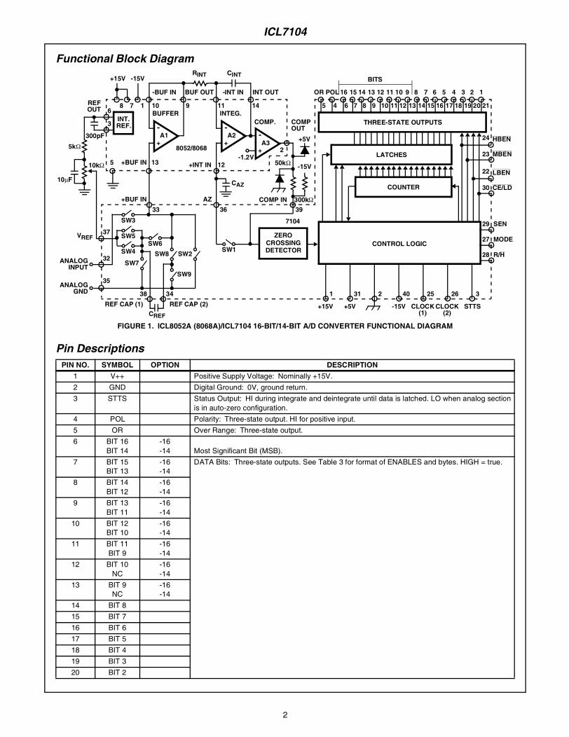
Functional Block Diagram
FIGURE 1. ICL8052A (8068A)/ICL7104 16-BIT/14-BIT A/D CONVERTER FUNCTIONAL DIAGRAM
A2+
-
A3+
-
INTEG.COMP.
A1+
-
BUFFER14119
INT OUT-INT INBUF OUT
10
-BUF IN
-1.2V2
50kΩ -15V
+5V
RINT CINT
1
-15V
78
+15V
CAZ
12+INT IN13
8052/8068
INT.REF.
6
3
+BUF IN5
REFOUT
5kΩ
10kΩ
300pF
10µF
COMPOUT
COMP IN 300kΩ393633
8 96 7 12 1310 11 16 1714 15 20 2118 195 4
14 1316 15 10 912 11 6 58 7 2 14 3OR POL
THREE-STATE OUTPUTS
LATCHES
COUNTER
24 HBEN
23 MBEN
22 LBEN
30 CE/LD
CONTROL LOGICZERO
CROSSINGDETECTOR
29
27
28
7104
+BUF IN AZ
SW3
SW5
SW4SW6
SW8 SW2
SW9
SW7
SW1
34
REF CAP (2)REF CAP (1)
38
CREF
37
32
35ANALOG
GND
ANALOGINPUT
VREF
SEN
MODE
R/H
BITS
3
STTS
26
CLOCK
25
CLOCK
40
-15V
21
+15V
31
+5V(2)(1)
Pin Descriptions PIN NO. SYMBOL OPTION DESCRIPTION
1 V++ Positive Supply Voltage: Nominally +15V.
2 GND Digital Ground: 0V, ground return.
3 STTS Status Output: HI during integrate and deintegrate until data is latched. LO when analog sectionis in auto-zero configuration.
4 POL Polarity: Three-state output. HI for positive input.
5 OR Over Range: Three-state output.
6 BIT 16BIT 14
-16-14 Most Significant Bit (MSB).
7 BIT 15BIT 13
-16-14
DATA Bits: Three-state outputs. See Table 3 for format of ENABLES and bytes. HIGH = true.
8 BIT 14BIT 12
-16-14
9 BIT 13BIT 11
-16-14
10 BIT 12BIT 10
-16-14
11 BIT 11BIT 9
-16-14
12 BIT 10NC
-16-14
13 BIT 9NC
-16-14
14 BIT 8
15 BIT 7
16 BIT 6
17 BIT 5
18 BIT 4
19 BIT 3
20 BIT 2
ICL7104

21 BIT 1 Least Significant Bit (LSB).
22 LBEN LOW BYTE ENABLE: If not in handshake mode (see pin 27) when LO (with CE/LD, pin 30)activates low-order byte outputs, BITS 1-8. When in handshake mode (see pin 27), serves as alow byte flag output. See Figures 11, 12, 13.
23 MBEN -16 MID BYTE ENABLE: Activates Bits 9-16, see LBEN (pin 22)
HBEN -14 HIGH BYTE ENABLE: Activates Bits 9-14, POL, OR, see LBEN (pin 22)
24 HBEN -16 HIGH BYTE ENABLE: Activates POL, OR, see LBEN (pin 22).
CLOCK3 -14 RC oscillator pin: Can be used as clock output.
25 CLOCK 1 Clock Input: External clock or ocsillator.
26 CLOCK 2 Clock Output: Crystal or RC oscillator.
27 MODE INPUT LO: Direct output mode where CE/LD, HBEN, MBEN and LBEN act as inputs directlycontrolling byte outputs. If pulsed HI causes immediate entry into handshake mode (see Figure13). If HI, enables CE/LD, HBEN, MBEN and LBEN as outputs. Handshake mode will be enteredand data output as in Figures 11 and 12 at conversion completion.
28 R/H RUN/HOLD: Input HI conversions continuously performed every 217(-16) or 215(-14) clockpulses. Input LO conversion in progress completed, converter will stop in Auto-Zero 7 countsbefore input integrate.
29 SEN SEND ENABLE: Input controls timing of byte transmission in handshake mode. HI indicates‘send’.
30 CE/LD CHIP ENABLE/ LOAD: WITH MODE (PIN 27) LO, CE/LD serves as a master output enable;when HI, the bit outputs and POL, OR are disabled. With MODE HI, pin serves as a LOAD strobe(-ve going) used in handshake mode. See Figures 11 and 12.
31 V+ Positive Logic Supply Voltage: Nominally +5V.
32 AN I/P Analog Input: High Side.
33 BUF IN Buffer Input: Buffer Analog to analog chip (ICL8052 or ICL8086).
34 REFCAP2 Reference Capacitor: Negative Side.
35 AN. GND Analog Ground: Input low side and reference low side.
36 A-Z Auto-Zero node.
37 VREF Voltage Reference: Input (positive side).
38 REFCAP1 Reference Capacitor: Positive side.
39 COMP-IN Comparator Input: From 8052/8068.
40 V- Negative Supply Voltage: Nominally -15V.
Pin Descriptions (Continued)
PIN NO. SYMBOL OPTION DESCRIPTION
ICL7104
3
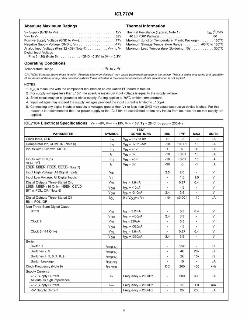
Absolute Maximum Ratings Thermal Information
V+ Supply (GND to V+) . . . . . . . . . . . . . . . . . . . . . . . . . . . . . . . 12VV++ to V- . . . . . . . . . . . . . . . . . . . . . . . . . . . . . . . . . . . . . . . . . . 32VPositive Supply Voltage (GND to V++). . . . . . . . . . . . . . . . . . . . 17VNegative Supply Voltage (GND to V-) . . . . . . . . . . . . . . . . . . . . -17VAnalog Input Voltage (Pins 32 - 39)(Note 4). . . . . . . . . . . . V++ to V-Digital Input Voltage
(Pins 2 - 30) (Note 5) . . . . . . . . . . . . (GND - 0.3V) to (V+ + 0.3V)
Operating ConditionsTemperature Range . . . . . . . . . . . . . . . . . . . . . . . . . . . .0oC to 70oC
Thermal Resistance (Typical, Note 1) θJA (oC/W)40 Ld PDIP Package . . . . . . . . . . . . . . 60
Maximum Junction Temperature (Plastic Package) . . . . . . . . 150oCMaximum Storage Temperature Range . . . . . . . . . . -65oC to 150oCMaximum Lead Temperature (Soldering, 10s) . . . . . . . . . . . . 300oC
CAUTION: Stresses above those listed in “Absolute Maximum Ratings” may cause permanent damage to the device. This is a stress only rating and operationof the device at these or any other conditions above those indicated in the operational sections of this specification is not implied.
NOTES:1. θJA is measured with the component mounted on an evaluation PC board in free air.2. For supply voltages less than ±15V, the absolute maximum input voltage is equal to the supply voltage.3. Short circuit may be to ground or either supply. Rating applies to 70oC ambient temperature.4. Input voltages may exceed the supply voltages provided the input current is limited to ±100µA.5. Connecting any digital inputs or outputs to voltages greater than V+ or less than GND may cause destructive device latchup. For this
reason it is recommended that the power supply to the ICL7104 be established before any inputs from sources not on that supply areapplied.
ICL7104 Electrical Specifications V+ = +5V, V++ = +15V, V- = -15V, TA = 25oC, fCLOCK = 200kHz
PARAMETER SYMBOLTEST
CONDITIONS MIN TYP MAX UNITS
Clock Input, CLK 1 IIN VIN = +5V to 0V ±2 ±7 ±30 µA
Comparator I/P, COMP IN (Note 6) IIN VIN = 0V to +5V -10 ±0.001 10 µA
Inputs with Pulldown, MODE IIH VIN = +5V 1 5 30 µA
IIL VIN = 0V -10 ±0.01 10 µA
Inputs with PullupsSEN, R/HLBEN, MBEN, HBEN, CE/LD (Note 7)
IIH VIN = +5V -10 ±0.01 10 µA
IIL VIN = 0V -30 -5 -1 µA
Input High Voltage, All Digital Inputs VIH 2.5 2.0 - V
Input Low Voltage, All Digital Inputs VIL - 1.5 1.0 V
Digital Outputs Three-Stated On, LBEN, MBEN (16 Only), HBEN, CE/LDBIT n, POL, OR (Note 8)
VOL IOL = 1.6mA - 0.27 0.4 V
VOH IOH = -10µA - 4.5 - V
VOH IOH = -240µA 2.4 3.5 - V
Digital Outputs Three-Stated OffBit n, POL, OR
IOL 0 ≤ VOUT ≤ V+ -10 ±0.001 +10 µA
Non Three-State Digital OutputSTTS VOL IOL = 3.2mA - 0.3 0.4 V
VOH IOH = -400µA 2.4 3.3 - V
Clock 2 VOL IOL= 320µA - 0.5 - V
VOH IOH = -320µA - 4.5 - V
Clock 3 (-14 Only) VOL IOL = 1.6mA - 0.27 0.4 V
VOH IOH = -320µA 2.4 3.5 - V
SwitchSwitch 1 rDS(ON) - 25k - ΩSwitches 2, 3 rDS(ON) - 4k 20k ΩSwitches 4, 5, 6, 7, 8, 9 rDS(ON) - 2k 10k ΩSwitch Leakage ID(OFF) - 15 - pA
Clock Frequency (Note 9) fCLOCK DC 200 400 kHz
Supply Currents+5V Supply CurrentAll outputs high impedance
I+ Frequency = 200kHz - 200 600 µA
+5V Supply Current I++ Frequency = 200kHz - 0.3 1.0 mA
-5V Supply Current I- Frequency = 200kHz - 25 200 µA
ICL7104
4

5
Supply Voltage RangeLogic Supply V+ Note 10 4 - 11 V
Positive Supply V++ 10 - 16 V
Negative Supply V- -16 - -10 V
NOTES:
6. This specification applies when not in Auto-Zero phase.
7. Apply only when these pins are inputs, i.e., the mode pin is low, and the 7104 is not in handshake mode.
8. Apply only when these pins are outputs, i.e., the mode pin is high, or the 7104 is in handshake mode.
9. Clock circuit shown in Figures 14 and 15.
10. V+ must not be more positive than V++.
System Electrical Specifications: ICL8068/ICL7104 V++ = +15V, V+ = +5V, V- = -15V, fCLOCK = 200kHz (Note 16)
PARAMETERTEST
CONDITIONS
ICL8068A/ICL7104-14 ICL8068A/ICL7104-16
UNITSMIN TYP MAX MIN TYP MAX
Zero Input Reading VIN = 0V, VREF = 2V -00000 ±00000 +00000 -00000 ±00000 +00000 Counts
Ratiometric Error (Note 13) VIN = VREF = 2V -1 0 1 -1 0 1 LSB
Linearity Over ± Full Scale (Error of Reading from Best Straight Line)
-4V ≤ VIN ≤ +4V - 0.5 1 - 0.5 1 LSB
Differential Linearity (Difference between Worst Case Step of Adjacent Counts and Ideal Step)
-4V ≤ VIN ≤ +4V - 0.01 - - 0.01 - LSB
Rollover Error (Difference in Reading for Equal Positive & Negative Voltage Near Full Scale)
-VIN = +VIN ≅ 4V - 0.5 1 - 0.5 1 LSB
Noise (P-P Value Not Exceeded 95% of Time)
VIN = 0V,Full Scale = 4V
- 2 - - 2 - µV
Leakage Current at Input (Note 14) VIN = 0V - 100 165 - 100 165 pA
Zero Reading Drift VIN = 0V,0oC to 70oC
- 0.5 - - 0.5 - µV/oC
Scale Factor Temperature Coefficient(Note 15)
VIN = 4V,0oC to 50oCext. ref. 0ppm/oC
- 2 5 - 2 5 ppm/oC
System Electrical Specifications: ICL8052/ICL7104 V++ = +15V, V+ = +5V, V- = -15V, fCLOCK = 200kHz
(Note 16)
PARAMETERTEST
CONDITIONS
ICL8052A/ICL7104-14 ICL8052A/ICL7104-16
UNITSMIN TYP MAX MIN TYP MAX
Zero Input Reading VIN = 0V, VREF = 2V -00000 ±00000 +00000 -00000 ±00000 +00000 Counts
Ratiometric Error (Note 15) VIN = VREF = 2V -1 0 1 -1 0 1 LSB
Linearity Over ± Full Scale (Error of Reading from Best Straight Line)
-4V ≤ VIN ≤ +4V - 0.5 1 - 0.5 1 LSB
Differential Linearity (Difference between Worst Case Step of Adjacent Counts and Ideal Step)
-4V ≤ VIN ≤ +4V - 0.01 - - 0.01 - LSB
Rollover Error (Difference in Reading for Equal Positive and Negative Voltage Near Full Scale)
-VIN = +VIN ≈ 4V - 0.5 1 - 0.5 1 LSB
Noise (Peak-to-Peak Value Not Exceeded 95% of Time)
VIN = 0V,Full Scale = 4V
- 30 - - 30 - µV
ICL7104 Electrical Specifications V+ = +5V, V++ = +15V, V- = -15V, TA = 25oC, fCLOCK = 200kHz (Continued)
PARAMETER SYMBOLTEST
CONDITIONS MIN TYP MAX UNITS
ICL7104

Leakage Current at Input (Note 14) VIN = 0V - 20 30 - 20 30 pA
Zero Reading Drift VIN = 0V,0oC to 70oC
- 0.5 - - 0.5 - µV/oC
Scale Factor Temperature Coefficient VIN = 4V,0oC to 50oCext. ref. 0ppm/oC
- 2 - - 2 - ppm/oC
NOTES:
11. Tested with low dielectric absorption integrating capacitor.
12. The input bias currents are junction leakage currents which approximately double for every 10oC increase in the junction temperature, TJ. Due to limited production test time, the input bias currents are measured with junctions at ambient temperature. In normal operationthe junction temperature rises above the ambient temperature as a result of internal power dissipation, PD. TJ = TA + RθJAPD whereRθJA is the thermal resistance from junction to ambient. A heat sink can be used to reduce temperature rise.
13. The temperature range can be extended to 70oC and beyond if the Auto-Zero and Reference capacitors are increased to absorb the high temperature leakage of the 8068. See note 14 above.
14. System Electrical Specifications are not tested; for reference only.
System Electrical Specifications: ICL8052/ICL7104 V++ = +15V, V+ = +5V, V- = -15V, fCLOCK = 200kHz
(Note 16) (Continued)
PARAMETERTEST
CONDITIONS
ICL8052A/ICL7104-14 ICL8052A/ICL7104-16
UNITSMIN TYP MAX MIN TYP MAX
FIGURE 2. FULL 18-BIT THREE-STATE OUTPUT
CE/LD HBEN MBEN LBEN
R/H
OR
POL
MSB
LSB
MODE
8052A/8068A
7104 -16
OR CHIP SELECT 2
CHIP SELECT 1
CONVERTCONTROL
18
≥18
FIGURE 3. VARIOUS COMBINATIONS OF BYTE DISABLES
CE/LD
HBEN MBEN LBEN
R/H
OR
POL
MSB
LSB
MODE
8052A/8068A
7104
CONVERT
2
CONTROL
CE/LD
HBEN MBEN LBEN
R/H
OR
POL
MSB
LSB
MODE
8052A/8068A
7104
CONVERT
CONTROL
CE/LD
HBEN MBEN LBEN
R/H
OR
POL
MSB
LSB
MODE
8052A/8068A
7104
CONVERT
CONTROL
8
8
2
16
10
8
ICL7104
6

7
FIGURE 4. DIRECT MODE TIMING DIAGRAM
DATAVALID
DATAVALID
DATAVALID
DATAVALID
DATAVALID
CE/LDAS INPUT
HBENAS INPUT
MBENAS INPUT
LBENAS INPUT
HIGH BYTEDATA
BYTEENABLE
LOW BYTEENABLE
MIDDLE
tBEA
tDAB tDHB
tDAC tDHC
tCEA
= HIGH IMPEDANCE
TABLE 1. DIRECT MODE TIMING REQUIREMENTS (Note: Not tested in production)
SYMBOL DESCRIPTION MIN TYP MAX UNIT
tBEA XBEN (Min) Pulse Width. - 300 - ns
tDAB Data Access Time from XBEN. - 300 - ns
tDHB Data Hold Time from XBEN. - 200 - ns
tCEA CE/LD Min. Pulse Width. - 350 - ns
tDAC Data Access Time from CE/LD. - 350 - ns
tDHC Data Hold Time from CE/LD. - 280 - ns
tCWH CLOCK 1 High Time. - 1000 - ns
TABLE 2. HANDSHAKE TIMING REQUIREMENTS (Note: Not tested in production)
SYMBOL DESCRIPTION MIN TYP MAX UNIT
tMW Mode Pulse (Min). - 20 - ns
tSM Mode Pin Set-Up Time. - -150 - ns
tME Mode Pin High to Low Z CE/LD High Delay. - 200 - ns
tMB Mode Pin High to XBEN Low Z (High) Delay. - 200 - ns
tCEL Clock 1 High to CE/LD Low Delay. - 700 - ns
tCEH Clock 1 High to CE/LD High Delay. - 600 - ns
tCBL Clock 1 High to XBEN Low Delay. - 900 - ns
tCBH Clock 1 High to XBEN High Delay. - 700 - ns
tCDH Clock 1 High to Data Enabled Delay. - 1100 - ns
tCDL Clock 1 Low to Data Disabled Delay. - 1100 - ns
tSS Send ENABLE Set-Up Time. - -350 - ns
tCBZ Clock 1 High to XBEN Disabled Delay. - 2000 - ns
tCEZ Clock 1 High to CE/LD Disabled Delay. - 2000 - ns
tCWH Clock 1 High Time. 1250 1000 - ns
ICL7104

Detailed Description
ANALOG SECTION
Figure 6 shows the equivalent Circuit of the Analog Sectionof both the ICL7104/8052 and the ICL7104/8068 in the 3different phases of operation. If the Run/Hold pin is left openor tied to V+, the system will perform conversions at a ratedetermined by the clock frequency: 131,072 for - 16 and32,368 for - 14 clock periods per cycle (see Figure 8conversion timing).
Auto-Zero Phase I (Figure 6A)
During Auto-Zero, the input of the buffer is shorted to analogground thru switch 2, and switch 1 closes a loop around theintegrator and comparator. The purpose of the loop is tocharge the Auto-Zero capacitor until the integrator output nolonger changes with time. Also, switches 4 and 9 rechargethe reference capacitor to VREF.
Input Integrate Phase II (Figure 6B)
During input integrate the Auto-Zero loop is opened and theanalog input is connected to the buffer input thru switch 3.(The reference capacitor is still being charged to VREFduring this time.) If the input signal is zero, the buffer,integrator and comparator will see the same voltage thatexisted in the previous sate (Auto-Zero). Thus the integratoroutput will not change but will remain stationary during theentire Input Integrate cycle. If VIN is not equal to zero, an
unbalanced condition exists compared to the Auto-Zerophase, and the integrator will generate a ramp whose slopeis proportional to VIN. At the end of this phase, the sign ofthe ramp is latched into the polarity F/F.
Deintegrate Phase III (Figures 6C and 6D)
During the Deintegrate phase, the switch drive logic uses theoutput of the polarity F/F in determining whether to closeswitches 6 and 9 or 7 and 8. If the input signal was positive,switches 7 and 8 are closed and a voltage which is VREFmore negative than during Auto-Zero is impressed on thebuffer input. Negative inputs will cause +VREF to be appliedto the buffer input via switches 6 and 9. Thus, the referencecapacitor generates the equivalent of a (+) reference or a (-)reference from the single reference voltage with negligibleerror. The reference voltage returns the output of the inte-grator to the zero-crossing point established in Phase I. Thetime, or number of counts, required to do this is proportionalto the input voltage. Since the Deintegrate phase can betwice as long as the Input integrate phase, the input voltagerequired to give a full scale reading = 2VREF.
NOTE: Once a zero crossing is detected, the system automaticallyreverts to Auto-Zero phase for the leftover Deintegrate time (unlessRUN/HOLD is manipulated, see RUN/HOLD input in detaileddescription, digital section).
FIGURE 5. HANDSHAKE MODE TIMING DIAGRAM
CLOCK 1 HL(PIN 25)
EITHER:MODE PIN
ORINTERNAL
LATCH PULSE IFMODE “HI”
HL
HL
UART
NORM
DON’T CARE DON’T CARE
DON’T CARE STABLE
DATA VALID, STABLE
DATA VALID, STABLE
EXT EXT
tMW
tSMtCWH
H
L
HL
HL
HL
INTERNALMODE
IGNORED IGNORED
CE/LD
SEN(EXTERNAL
SIGNAL)
HBEN
O/R, POL01-14
LBEN
BITS 1-5
tME
tMB
tCEL tCEH
tSS
tCBL
tCDH tCDL
tCBH tCBZ
tCEZ
THREE-STATE WITH PULLUPTHREE-STATE-16 HAS EXTRA (MBEN) PHASE
HANDSHAKE MODE ORTRIGGERED BY
ICL7104
8

9
FIGURE 6A. PHASE I AUTO-ZERO
FIGURE 6B. PHASE II INTEGRATE INPUT
FIGURE 6C. PHASE III + DEINTEGRATE
A2+
-
A3+
-
INTEGRATORCOMP.
A1+
-
BUFFER
CINT
1
RINT
CAZ
ZEROCROSS.
DET.
POL CL
2
3
6
7
8
9
ANI/P
CL
ZEROCROSSING
F/F
QD
VREFCREF
- +4
A2+
-
A3+
-
INTEGRATORCOMP.
A1+
-
BUFFER
CINT
1
RINT
CAZ
ZEROCROSS.
DET.
POL CL
2
3
6
7
8
9
ANI/P
CL
ZEROCROSSING
F/F
QD
CL
POLF/F
QD
PHASE II
POL
VREFCREF
- +4
A2+
-
A3+
-
INTEGRATORCOMP.
A1+
-
BUFFER
CINT
1
RINT
CAZ
ZEROCROSS.
DET.
POL CL
2
3
6
7
8
9
+ANI/P
CL
ZEROCROSSING
F/F
QD
VREFCREF
- +4
ICL7104
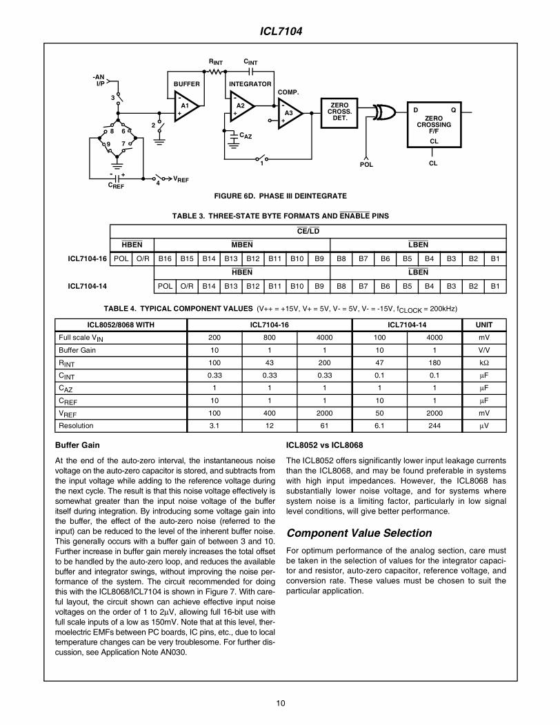
Buffer Gain
At the end of the auto-zero interval, the instantaneous noisevoltage on the auto-zero capacitor is stored, and subtracts fromthe input voltage while adding to the reference voltage duringthe next cycle. The result is that this noise voltage effectively issomewhat greater than the input noise voltage of the bufferitself during integration. By introducing some voltage gain intothe buffer, the effect of the auto-zero noise (referred to theinput) can be reduced to the level of the inherent buffer noise.This generally occurs with a buffer gain of between 3 and 10.Further increase in buffer gain merely increases the total offsetto be handled by the auto-zero loop, and reduces the availablebuffer and integrator swings, without improving the noise per-formance of the system. The circuit recommended for doingthis with the ICL8068/ICL7104 is shown in Figure 7. With care-ful layout, the circuit shown can achieve effective input noisevoltages on the order of 1 to 2µV, allowing full 16-bit use withfull scale inputs of a low as 150mV. Note that at this level, ther-moelectric EMFs between PC boards, IC pins, etc., due to localtemperature changes can be very troublesome. For further dis-cussion, see Application Note AN030.
ICL8052 vs ICL8068
The ICL8052 offers significantly lower input leakage currentsthan the ICL8068, and may be found preferable in systemswith high input impedances. However, the ICL8068 hassubstantially lower noise voltage, and for systems wheresystem noise is a limiting factor, particularly in low signallevel conditions, will give better performance.
Component Value Selection
For optimum performance of the analog section, care mustbe taken in the selection of values for the integrator capaci-tor and resistor, auto-zero capacitor, reference voltage, andconversion rate. These values must be chosen to suit theparticular application.
FIGURE 6D. PHASE III DEINTEGRATE
A2+
-
A3+
-
INTEGRATORCOMP.
A1+
-
BUFFER
CINT
1
RINT
CAZ
ZEROCROSS.
DET.
POL CL
2
3
6
7
8
9
-ANI/P
CL
ZEROCROSSING
F/F
QD
VREFCREF
- +4
TABLE 3. THREE-STATE BYTE FORMATS AND ENABLE PINS
CE/LD
HBEN MBEN LBEN
ICL7104-16 POL O/R B16 B15 B14 B13 B12 B11 B10 B9 B8 B7 B6 B5 B4 B3 B2 B1
HBEN LBEN
ICL7104-14 POL O/R B14 B13 B12 B11 B10 B9 B8 B7 B6 B5 B4 B3 B2 B1
TABLE 4. TYPICAL COMPONENT VALUES (V++ = +15V, V+ = 5V, V- = 5V, V- = -15V, fCLOCK = 200kHz)
ICL8052/8068 WITH ICL7104-16 ICL7104-14 UNIT
Full scale VIN 200 800 4000 100 4000 mV
Buffer Gain 10 1 1 10 1 V/V
RINT 100 43 200 47 180 kΩ
CINT 0.33 0.33 0.33 0.1 0.1 µF
CAZ 1 1 1 1 1 µF
CREF 10 1 1 10 1 µF
VREF 100 400 2000 50 2000 mV
Resolution 3.1 12 61 6.1 244 µV
ICL7104
10

Integrating Resistor
The integrating resistor is determined by the full scale inputvoltage and the output current of the buffer used to chargethe integrator capacitor. This current should be smallcompared to the output short circuit current such thatthermal effects are kept to a minimum and linearity is notaffected. Values of 5 to 40µA give good results with anominal of 20µA. The exact value may be chosen by:
NOTE: If gain is used in the buffer amplifier then
Integrating Capacitor
The product of integrating resistor and capacitor is selected
to give 9 volt swing for full scale inputs. This is a compromisebetween possibly saturating the integrator (at +14 volts) dueto tolerance build-up between the resistor, capacitor andclock and the errors a lower voltage swing could induce dueto offsets referred to the output of the comparator. Ingeneral, the value of CINT is given by:
A very important characteristic of the integrating capacitor isthat it have low dielectric absorption to prevent roll-over orratiometric errors. A good test for dielectric absorption is touse the capacitor with the input tied to the reference.
This ratiometric condition should read half scale (100...000)and any deviation is probably due to dielectric absorption.Polypropylene capacitors give undetectable errors at rea-sonable cost. Polystyrene and polycarbonate capacitorsmay also be used in less critical applications.
FIGURE 7. ADDING BUFFER GAIN TO ICL8068
A2+
-
A3+
-
INTEG.COMP.
A1+
-
BUFFER14119
INT OUT-INT INBUF OUT
10
-BUF IN
-1.2V2
-15V
+5V
RINT CINT
1
-15V
78
+15V
12+INT IN13
8068
INT.REF.
6
3
+BUF IN5
REFOUT
5kΩ
10kΩ
300pF COMPOUT
100kΩ
10-50K
TO ICL7104
COUNTS
PHASE I PHASE II PHASE III
-16 32768 32768 65536
-14 8192 8192 16384
FIGURE 8. CONVERSION TIMING
POLARITYDETECTED
ZERO CROSSINGOCCURS
ZERO CROSSINGDETECTED
DEINT PHASE IIIINT PHASE IIAZ PHASE I AZ
INTEGRATOROUTPUT
INTERNAL CLOCK
INTERNAL LATCH
STATUS OUTPUT
NUMBER OF COUNTS TO ZERO CROSSINGPROPORTIONAL TO VIN
AFTER ZERO CROSSING,ANALOG SECTION WILLBE IN AUTOZEROCONFIGURATION
RINTfull scale voltage (see note)
20µA-------------------------------------------------------------------------=
RINTBufferGain( ) (full scale voltage)
20µA----------------------------------------------------------------------------------------=
CINT
(32768 for - 16)(8192 for -14)
20µA× clock period×
Integrator Output Voltage Swing----------------------------------------------------------------------------------------------------------=
ICL7104
11

12
Auto-Zero and Reference Capacitor
The size of the auto-zero capacitor has some influence onthe noise of the system, a large capacitor giving less noise.The reference capacitor should be large enough such thatstray capacitance to ground from its nodes is negligible.
NOTE: When gain is used in the buffer amplifier the referencecapacitor should be substantially larger than the auto-zero capacitor.As a rule of thumb, the reference capacitor should be approximatelythe gain times the value of the auto-zero capacitor. The dielectricabsorption of the reference cap and auto-zero cap are only importantat power-on or when the circuit is recovering from an overload. Thus,smaller or cheaper caps can be used here if accurate readings arenot required for the first few seconds of recovery.
Reference Voltage
The analog input required to generate a full scale output isVIN = 2VREF.
The stability of the reference voltage is a major factor in theoverall absolute accuracy of the converter. The resolution ofthe ICL7104 at 16 bits is one part in 65536, or 15.26ppm.Thus, if the reference has a temperature coefficient of50ppm/C (on board reference) a temperature change of 1/3Cwill introduce a one-bit absolute error. For this reason, it is rec-ommended that an external high quality reference be usedwhere the ambient temperature is not controlled or wherehigh-accuracy absolute measurements are being made.
Detailed Description
DIGITAL SECTION
The digital section includes the clock oscillator circuit, a16-bit or 14-bit binary counter with output latches and TTL-compatible three-state output drivers, polarity, over-range
and control logic and UART handshake logic, as shown inthe Block Diagram Figure 9 (16-bit version shown).
Throughout this description, logic levels will be referred to as“low” or “high”. The actual logic levels are defined under“ICL7104 Electrical Specification”. For minimum power con-sumption, all inputs should swing from GND (low) to V+(high). Inputs driven from TTL gates should have 3 - 5kΩpullup resistors added for maximum noise immunity.
MODE Input
The MODE input is used to control the output mode of theconverter. When the MODE pin is connected to GND or leftopen (this input is provided with a pulldown resistor toensure a low level when the pin is left open), the converter isin its “Direct” output mode, where the output data is directlyaccessible under the control of the chip and byte enableinputs. When the MODE input is pulsed high, the converterenters the UART handshake mode and outputs the data inthree bytes for the 7104-16 or two bytes for the 7104-14 thenreturns to “direct” mode. When the MODE input is left high,the converter will output data in the handshake mode at theend of every conversion cycle. (See section entitled “Hand-shake Mode” for further details).
STATUS Output
During a conversion cycle, the STATUS output goes high atthe beginning of Input Integrate (Phase II), and goes lowone-half clock period after new data from the conversion hasbeen stored in the output latches. See Figure 8 for details ofthis timing. This signal may be used as a “data valid” flag(data never changes while STATUS is low) to drive inter-rupts, or for monitoring the status of the converter.
TABLE 5. THREE-STATE BYTE FORMATS AND ENABLE PINS
CE/LD
HBEN MBEN LBEN
ICL7104-16 POL O/R B16 B15 B14 B13 B12 B11 B10 B9 B8 B7 B6 B5 B4 B3 B2 B1
HBEN LBEN
ICL7104-14 POL O/R B14 B13 B12 B11 B10 B9 B8 B7 B6 B5 B4 B3 B2 B1
ICL7104

Run/Hold Input
When the Run/Hold input is connected to V+ or left open(this input has pullup resistor to ensure a high level when thepin is left open), the circuit will continuously performconversion cycles, updating the output latches at the end ofevery Deintegrate (Phase III) portion of the conversion cycle(See Figure 8). (See under “Handshake Mode” forexception.) In this mode of operation, the conversion cyclewill be performed in 131,072 for 7104-16 and 32768 for7104-14 clock periods, regardless of the resulting value.
If Run/Hold goes low at any time during Deintegrate (PhaseIII) after the zero crossing has occurred, the circuit willimmediately terminate Deintegrate and jump to Auto-Zero.This feature can be used to eliminate the time spent inDeintegrate after the zero-crossing. If Run/Hold stays orgoes low, the converter will ensure a minimum Auto-Zerotime, and then wait in Auto-Zero until the Run/Hold inputgoes high. The converter will begin the Integrate (Phase II)portion of the next conversion (and the STATUS output willgo high) seven clock periods after the high level is detected
at Run/Hold. See Figure 10 for details.
Using the Run/Hold input in this manner allows an easy“convert on demand” interface to be used. The convertermay be held at idle in Auto-Zero with Run/Hold low. WhenRun/Hold goes high the conversion is started, and when theSTATUS output goes low the new data is valid (or trans-ferred) to the UART - see Handshake Mode). Run/Hold maynow go low terminating Deintegrate and ensuring a minimumAuto-Zero time before stopping to wait for the nextconversion. Alternately, Run/Hold can be used to minimizeconversion time by ensuring that it goes low during Deinte-grate, after zero crossing, and goes high after the hold pointis reached. The required activity on the Run/Hold input canbe provided by connecting it to the CLOCK3 (-14), CLOCK2(-16) Output. In this mode the conversion time is dependenton the input value measured. Also refer to Intersil Applica-tion Bulletin A030 for a discussion of the effects this will haveon Auto-Zero performance.
If the Run/Hold input goes low and stays low during Auto-Zero (Phase I), the converter will simply stop at the end of
FIGURE 9. DIGITAL SECTION
HBEN
MBEN
LBEN
CE/LDOSCILLATOR
27
SEND
21
MODE
25
CLOCK
23
CLOCK
242
STATUS
26
R/H(2) (3)
AND CLOCKCIRCUITRY
18/16 THREE-STATE OUTPUTS
18/16 LATCHES
18/16 BIT COUNTER
LATCH
CLOCK
HANDSHAKELOGIC
(-16 ONLY)
CONVERSIONCONTROL
LOGIC
INITIALCLEAR
CLOCK(1)
COMP OUTAZINTDEINT(+)DEINT(-)
TOANALOGSECTION
FIGURE 10. RUN/HOLD OPERATION
DEINT TERMINATEDAT ZERO CROSSING STATIC IN
HOLD STATE INTPHASE
7 COUNTS
INTEGRATOROUTPUT
INTERNALCLOCK
INTERNALLATCH
STATUSOUTPUT
RUN/HOLDINPUT
DETECTION
-14
7161
8185
-16
28665
32761
OPTION
MIN
MAX
ICL7104
13
14
the Auto-Zero and wait for Run/Hold to go high. As above,Integrate (Phase II) begins seven clock periods after thehigh level is detected.
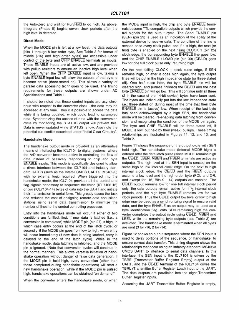
Direct Mode
When the MODE pin is left at a low level, the data outputs[bits 1 through 8 low order byte, See Table 3 for format ofmiddle (-16) and high order bytes] are accessible undercontrol of the byte and CHIP ENABLE terminals as inputs.These ENABLE inputs are all active low, and are providedwith pullup resistors to ensure an inactive high level whenleft open. When the CHIP ENABLE input is low, taking abyte ENABLE input low will allow the outputs of that byte tobecome active (three-stated on). This allows a variety ofparallel data accessing techniques to be used. The timingrequirements for these outputs are shown under ACSpecifications and Table 1.
It should be noted that these control inputs are asynchro-nous with respect to the converter clock - the data may beaccessed at any time. Thus it is possible to access the datawhile it is being updated, which could lead to scrambleddata. Synchronizing the access of data with the conversioncycle by monitoring the STATUS output will prevent this.Data is never updated while STATUS is low. Also note thepotential bus conflict described under “Initial Clear Circuitry”.
Handshake Mode
The handshake output mode is provided as an alternativemeans of interfacing the ICL7104 to digital systems, wherethe A/D converter becomes active in controlling the flow ofdata instead of passively responding to chip and byteENABLE inputs. This mode is specifically designed to allowa direct interface between the ICL7104 and industry-stan-dard UARTs (such as the Intersil CMOS UARTs, IM6402/3)with no external logic required. When triggered into thehandshake mode, the ICL7104 provides all the control andflag signals necessary to sequence the three (ICL7106-16)or two (ICL7104-14) bytes of data into the UART and initiatetheir transmission in serial form. This greatly eases the taskand reduces the cost of designing remote data acquisitionstations using serial data transmission to minimize thenumber of lines to the central controlling processor.
Entry into the handshake mode will occur if either of twoconditions are fulfilled; first, if new data is latched (i.e., aconversion is completed) while MODE pin (pin 27) is high, inwhich case entry occurs at the end of the latch cycle; orsecondly, if the MODE pin goes from low to high, when entrywill occur immediately (if new data is being latched, entry isdelayed to the end of the latch cycle). While in thehandshake mode, data latching is inhibited, and the MODEpin is ignored. (Note that conversion cycles will continue inthe normal manner). This allows versatile initiation of hand-shake operation without danger of false data generation; ifthe MODE pin is held high, every conversion (other thanthose completed during handshake operations) will start anew handshake operation, while if the MODE pin is pulsedhigh, handshake operations can be obtained “on demand.”
When the converter enters the handshake mode, or when
the MODE input is high, the chip and byte ENABLE termi-nals become TTL-compatible outputs which provide the con-trol signals for the output cycle. The Send ENABLE pin(SEN) (pin 29) is used as an indication of the ability of theexternal device to receive data. The condition of the line issensed once every clock pulse, and if it is high, the next (orfirst) byte is enabled on the next rising CLOCK 1 (pin 25)clock edge, the corresponding byte ENABLE line goes low,and the CHIP ENABLE / LOAD pin (pin 30) (CE/LD) goeslow for one full clock pulse only, returning high.
On the next falling CLOCK 1 clock pulse edge, if SENremains high, or after it goes high again, the byte outputlines will be put in the high impedance state (or three-statedoff). One half pulse later, the byte ENABLE pin will becleared high, and (unless finished) the CE/LD and the nextbyte ENABLE pin will go low. This will continue until all three(2 in the case of the 14-bit device) bytes have been sent.The bytes are individually put into the low impedance statei.e.: three-stated on during most of the time that their byteENABLE pin is (active) low. When receipt of the last bytehas been acknowledged by a high SEN, the handshakemode will be cleared, re-enabling data latching from conver-sion, and recognizing the condition of the MODE pin again.The byte and CHIP ENABLE will be three-stated off, ifMODE is low, but held by their (weak) pullups. These timingrelationships are illustrated in Figures 11, 12, and 13, andTable 2.
Figure 11 shows the sequence of the output cycle with SENheld high. The handshake mode (Internal MODE high) isentered after the data latch pulse (since MODE remains highthe CE/LD, LBEN, MBEN and HBEN terminals are active asoutputs). The high level at the SEN input is sensed on thesame high to low internal clock edge. On the next to highinternal clock edge, the CE/LD and the HBEN outputsassume a low level and the high-order byte (POL and OR,and except for -16, Bits 9 - 14) outputs are enabled. TheCE/LD output remains low for one full internal clock periodonly, the data outputs remain active for 11/2 internal clockperiods, and the high byte ENABLE remains low for twoclock periods. Thus the CE/LD output low level or low to highedge may be used as a synchronizing signal to ensure validdata, and the byte ENABLE as an output may be used as abyte identification flag. With SEN remaining high the con-verter completes the output cycle using CE/LD, MBEN andLBEN while the remaining byte outputs (see Table 3) areactivated. The handshake mode is terminated when all bytesare sent (3 for -16, 2 for -14).
Figure 12 shows an output sequence where the SEN input isused to delay portions of the sequence, or handshake, toensure correct data transfer. This timing diagram shows therelationships that occur using an industry-standard IM6402/3CMOS UART to interface to serial data channels. In thisinterface, the SEN input to the ICL7104 is driven by theTBRE (Transmitter Buffer Register Empty) output of theUART, and the CE/LD terminal of the ICL7104 drives theTBRL (Transmitter Buffer Register Load) input to the UART.The data outputs are paralleled into the eight TransmitterBuffer Register inputs.
Assuming the UART Transmitter Buffer Register is empty,
ICL7104

the SEN input will be high when the handshake mode isentered after new data is stored. The CE/LD and HBEN ter-minals will go low after SEN is sensed, and the high orderbyte outputs become active. When CE/LD goes high at theend of one clock period, the high order byte data is clockedinto the UART Transmitter Buffer Register. The UART TBREoutput will now go low, which halts the output cycle with theHBEN output low, and the high order byte outputs active.When the UART has transferred the data to the TransmitterRegister and cleared the Transmitter Buffer Register, theTBRE returns high. On the next ICL7104 internal clock highto low edge, the high order byte outputs are disabled, andone-half internal clock later, the HBEN output returns high.At the same time, the CE/LD and MBEN (-16) or LBEN out-puts go low, and the corresponding byte outputs becomeactive. Similarly, when the CE/LD returns high at the end ofone clock period, the enabled data is clocked into the UARTTransmitter Buffer Register, and TBRE again goes low.When TBRE returns to a high it will be sensed on the nextICL7104 internal clock high to low edge, disabling the dataoutputs. For the 16-bit device, the sequence is repeated for
LBEN. One-half internal clock later, the handshake mode willbe cleared, and the chip and byte ENABLE terminals returnhigh and stay active (as long as MODE stays high).
With the MODE input remaining high as in these examples,the converter will output the results of every conversionexcept those completed during a handshake operation. Bytriggering the converter into handshake mode with a low tohigh edge on the MODE input, handshake output sequencesmay be performed on demand. Figure 13 shows ahandshake output sequence triggered by such an edge. Inaddition, the SEN input is shown as being low when the con-verter enters handshake mode. In this case, the whole out-put sequence is controlled by the SEN input, and thesequence for the first (high order) byte is similar to thesequence for the other bytes. This diagram also shows theoutput sequence taking longer than a conversion cycle. Notethat the converter still makes conversions, with the STATUSoutput and Run/Hold input functioning normally. The onlydifference is that new data will not be latched when inhandshake mode, and is therefore lost.
FIGURE 11. HANDSHAKE WITH SEN HELD POSITIVE
DATA VALID
DATA VALID
DATA VALID
THREE-STATE WITH PULLUPTHREE-STATE HIGH IMPEDANCEDON’T CARE
INTEGRATOR OUTPUT
INTERNAL CLOCK
INTERNAL LATCH
STATUS OUTPUT
MODE INPUT
INTERNAL MODE
SEN INPUT
CE/LOAD
UART
HIGH BYTE DATA
LOW BYTE DATA
LOW BYTE DATA
NORM
MODE HIGH ACTIVATESCE/LD, HBEN, LBEN
HBEN
LBEN
LBEN
SENSEDSEN
ZERO-CROSSING DETECTED
ZERO-CROSSING OCCURS
MODE LOW NOT IN HANDSHAKE MODEDISABLES OUTPUTS CE/LD, HBEN, MBEN, LBEN
SENSEDSEN
TERMINATESUART MODE
FOR -16 MBEN SEQUENCE INSERTED HERE
ICL7104
15

16
FIGURE 12. HANDSHAKE - TYPICAL UART INTERFACE TIMING
DATA VALID
THREE-STATE HIGH IMPEDANCEDON’T CARE
INTEGRATOR
INTERNAL
INTERNAL
STATUS
MODE
INTERNAL
SEN INPUT
CE/LOAD
UART
HIGH BYTE
MIDDLE
LOW BYTE
NORM
HBEN
MBEN
LBEN
ZERO-CROSSING DETECTED
ZERO-CROSSING OCCURS
OUTPUT
CLOCK
LATCH
OUTPUT
INPUT
MODE
DATA
BYTE DATA
DATA
DATA VALID
DATA VALID
(UART TBRE)
(UART TBRL)
ICL7104

Initial Clear Circuitry
The internal logic of the 7104 is supplied by an internalregulator between V++ and Digital Ground. The regulatorincludes a low-voltage detector that will clear variousregisters. This is intended to ensure that on initial power-up,the control logic comes up in Auto-Zero, with the 2nd, 3rd,and 4th MSB bits cleared, and the “mode” F/F cleared (i.e.,in “direct” mode). This, however, will also clear these regis-ters if the supply voltage “glitches” to a low enough value.Additionally, if the supply voltage comes up too fast, thisclear pulse may be too narrow for reliable clearing. In gen-eral, this is not a problem, but if the UART internal “MODE”F/F should come up set, the byte and chip ENABLE lines willbecome active outputs. In many systems this could lead tobus conflicts, especially in non-handshake systems. In anycase, SEN should be high (held high for non-handshake sys-tems) to ensure that the MODE F/F will be cleared as fast aspossible (see Figure 11 for timing). For these and otherreasons, adequate supply bypass is recommended.
Oscillator
The ICL7104-14 is provided with a versatile three terminaloscillator to generate the internal clock. The oscillator maybe overdriven, or may be operated as an RC or crystaloscillator.
Figure 14 shows the oscillator configured for RC operation.The internal clock will be of the same frequency and phaseas the voltage on the CLOCK 3 pin. The resistor andcapacitor should be connected as shown. The circuit willoscillate at a frequency given by f = 0.45/RC. A 50 - 100kΩresistor is recommended for useful ranges of frequency. Foroptimum 60Hz line rejection, the capacitor value should bechosen such that 32768 (-16), 8192 (-14) clock periods isclose to an integral multiple of the 60Hz period.
As a result of pin count limitations, the ICL7104-16 has onlyCLOCK 1 and CLOCK 2 available, and cannot be used asan RC oscillator. The internal clock will correspond to theinverse of the signal on CLOCK 2. Figure 15 shows a crystaloscillator circuit, which can be used with both 7104 versions.If an external clock is to be used, it should be applied toCLOCK 1. This internal clock will correspond to the signalapplied to this pin.
FIGURE 13. HANDSHAKE TRIGGERED BY MODE
DATA VALID
INTERNAL
INTERNAL
STATUS
MODE
INTERNAL
SEN INPUT
CE/LOAD
UART
HIGH BYTE
MIDDLE
LOW BYTE
NORM
HBEN
MBEN
LBEN
ZERO-CROSSING DETECTED
ZERO-CROSSING OCCURS
CLOCK
LATCH
OUTPUT
INPUT
MODE
DATA
BYTE DATA
DATA
DATA VALID
DATA VALID
STATUS OUTPUT UNAFFECTEDBY UART MODE
LATCH PULSE INHIBITEDIN UART MODE
THREE-STATE WITH PULLUPTHREE-STATE HIGH IMPEDANCEDON’T CARE
POSITIVE TRANSITIONCAUSES ENTRY INTOUART MODE
DEINT PHASE III
AS OUTPUT
NOTE: Clock 3 has the same output drive as the bit outputs.
FIGURE 14. RC OSCILLATOR (ICL7104-14 ONLY)
CLOCK
25 26
RC
2CLOCK
3CLOCK
1
24
fOSC = 0.45/RC
FIGURE 15. CRYSTAL OSCILLATOR
CLOCK
25 26
2CLOCK
1
V+
†CAPACITOR VALUEDEPENDS ON CRYSTALTYP 0-30pF
CRYSTAL
†
ICL7104
17
18
ICL7104
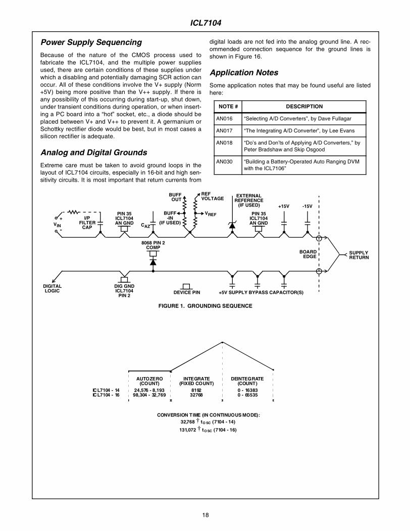
Power Supply Sequencing
Because of the nature of the CMOS process used tofabricate the ICL7104, and the multiple power suppliesused, there are certain conditions of these supplies underwhich a disabling and potentially damaging SCR action canoccur. All of these conditions involve the V+ supply (Norm+5V) being more positive than the V++ supply. If there isany possibility of this occurring during start-up, shut down,under transient conditions during operation, or when insert-ing a PC board into a “hot” socket, etc., a diode should beplaced between V+ and V++ to prevent it. A germanium orSchottky rectifier diode would be best, but in most cases asilicon rectifier is adequate.
Analog and Digital Grounds
Extreme care must be taken to avoid ground loops in thelayout of ICL7104 circuits, especially in 16-bit and high sen-sitivity circuits. It is most important that return currents from
digital loads are not fed into the analog ground line. A rec-ommended connection sequence for the ground lines isshown in Figure 16.
Application Notes
Some application notes that may be found useful are listedhere:
NOTE # DESCRIPTION
AN016 “Selecting A/D Converters”, by Dave Fullagar
AN017 “The Integrating A/D Converter”, by Lee Evans
AN018 “Do’s and Don’ts of Applying A/D Converters,” by Peter Bradshaw and Skip Osgood
AN030 “Building a Battery-Operated Auto Ranging DVM with the ICL7106”
FIGURE 1. GROUNDING SEQUENCE
DEVICE PINDIG GNDICL7104
PIN 2
DIGITALLOGIC
VIN
I/P+
-FILTER
CAP
8068 PIN 2COMP
PIN 35ICL7104AN GND CAZ
VREFBUFF-IN
(IF USED)
REFVOLTAGE
BUFFOUT
EXTERNALREFERENCE
(IF USED)
PIN 35ICL7104AN GND
+15V -15V
+5V SUPPLY BYPASS CAPACITOR(S)
SUPPLYRETURN
BOARDEDGE
AUTOZERO(COUNT)
24,576 - 8,19398,304 - 32,769
INTEGRATE(FIXED COUNT)
819232768
DEINTEGRATE(COUNT)0 - 163830 - 65535
ICL7104 - 14ICL7104 - 16
CONVERSION TIME (IN CONTINUOUS MODE):32,768 † tO SC (7104 - 14)
131,072 † tO SC (7104 - 16)

ICL7104
ICL7104 with ICL8052/8068 Integrating A/D Converter Equations• Oscillator
CRYSTAL or RC (RC on -14 Part Only)fOSC (Typ) 200kHzfOSC = 0.45/RC (ICL7104-14 Only)COSC > 50pF and ROSC > 50K
• Oscillator Period
tOSC = 1/fOSC
• Integration Clock Frequency
fCLOCK = fOSC
• Integration Period
tINT = 8192 x tOSC (7104-14)tINT = 32768 x tOSC (7104-16)
• 60/50Hz Rejection Criterion
tINT/t60Hz or tINT/t50Hz = Integer
• Optimum Integration Current
IINT = 20µA
• Full Scale Analog Input Voltage
VINFS (Typ) = 200mV to 2V = 2VREF
• Integrate Resistor
• Integrate Capacitor
• Integrator Output Voltage
VINT (Typ) = 9V
• Output Count
• Output Type:
Binary Amplitude with Polarity and Overrange Bits.
• Power Supply: ±15V, +5V
V++ = +15VV- = -15VV+ = +5VVREF ≅ 1.75VIf VREF not used, float output pin.
• Auto Zero Capacitor Values
0.01µF < CAZ < 1µF
• Reference Capacitor Value
• CREF = (Buffer Gain) x CAZ
RINT
BufferGain( ) VINFS×IINT
-------------------------------------------------------------=
CINT
tINT( ) IINT( )
VINT--------------------------------=
VINT
tINT( ) IINT( )CINT
--------------------------------=
Count 8192VIN
VREF---------------× (7104-14)=
Count 32768VIN
VREF---------------× (7104-16)=
19