ibm research reportdomino.watson.ibm.com/library/cyberdig.nsf/papers/dffc51...pradip bose and jude...
TRANSCRIPT

RC23048 (W0312-122) December 29, 2003Computer Science
IBM Research Report
RAMP: A Model for Reliability Aware MicroProcessor Design
Jayanth Srinivasan, Sarita V. AdveDepartment of Computer Science
University of Illinois at Urbana-Champaign
Pradip Bose, Jude Rivers, Chao-Kun HuIBM Research Division
Thomas J. Watson Research CenterP.O. Box 218
Yorktown Heights, NY 10598
Research DivisionAlmaden - Austin - Beijing - Haifa - India - T. J. Watson - Tokyo - Zurich
LIMITED DISTRIBUTION NOTICE: This report has been submitted for publication outside of IBM and will probably be copyrighted if accepted for publication. It has been issued as a ResearchReport for early dissemination of its contents. In view of the transfer of copyright to the outside publisher, its distribution outside of IBM prior to publication should be limited to peer communications and specificrequests. After outside publication, requests should be filled only by reprints or legally obtained copies of the article (e.g. , payment of royalties). Copies may be requested from IBM T. J. Watson Research Center , P.O. Box 218, Yorktown Heights, NY 10598 USA (email: [email protected]). Some reports are available on the internet at http://domino.watson.ibm.com/library/CyberDig.nsf/home .

RAMP: A Model forReliability AwareM icroProcessor Design∗
Jayanth Srinivasan, Sarita V. Adve Pradip Bose, Jude Rivers, Chao-Kun HuUniversity of Illinois at Urbana-Champaign IBM T.J. WatsonResearch Center
Department of Computer Science Yorktown Heights,NY{srinivsn,sadve}@cs.uiuc.edu, {pbose,jarivers,haohu}@us.ibm.com
The authors would like to acknowledge significant help from:Philip Emma, Barry Linder, and Ernest Y. Wu
IBM Corp.
Abstract
This report introducesRAMP , an architectural model for long-term processor reliability measure-ment. With aggresive transistor scaling and increasing processor power and temperature, reliability dueto wear-out mechanisms is expected to become a significant issue in microprocessor design. Reliabil-ity awareness at the microarchitectural design stage will soon be a neccessity and RAMP provides aconvenient abstraction to do so.
RAMP models chip wide mean time to failure as a function of thefailure rates of individual structureson chip due to different failure mechanisms, and can be used to evaluate the reliability implications ofdifferent applications, architectural features, and processor designs.
RAMP is a self-standing module which can be attached to architectural simulators which gener-ate power and temperature measurements, and has currently been ported to IBM’s Turandot processorsimulator and the RSIM architectural simulator.
1 Motivation
Ensuring long-term reliability is an essential goal for allmicroprocessor manufacturers. Although providing
huge benefits in microprocessor performance, advances in technology are accelerating the onset of reliability
problems and are causing a resultant reduction in processorlifetimes. With device miniaturization, design
and process error margins are shrinking, which in turn impacts device characteristics and reliability. In order
to maintain performance goals, semiconductor design and manufacturing are undergoing changes that will
∗Jayanth Srinivasan is a PhD student at UIUC under the guidance of Sarita Adve. This work was done when Jayanth was anintern at IBM T.J. Watson Research Center during Summer 2003. Pradip Bose and Jude Rivers were Jayanth’s mentors at IBM.
1

threaten the nearly unlimited lifetime and high reliability that customers have come to expect. This has
led the ITRS to predict the onset of significant reliability problems in the future, and at a pace that has not
been seen in the past. It is expected that in the future, product cost and performance requirements will be
substantially affected and, in many cases, superseded by reliability constraints [6].
The introduction of new materials, processes and devices, coupled with voltage scaling limitations and
increasing power consumption will impose many new reliability challenges. Specifically, the two main
challenges to maintaining reliability are: (1)the continued increase in die size and number of transistors, and
(2)the constant scaling of transistors for performance. [39, 6, 7] . Although transistor density is increasing,
new features and increasing functionality cause the die size and transistor count to grow rapidly1. More
transistors result in more failures which results in lower lifetimes. Increasing power consumption and in-
creasing transistor density are causing higher temperatures on chip resulting in failure acceleration. Scaling
to smaller transistors increases failure rates by shrinking the thickness of dielectrics (both gate dielectrics
and inter layer dielectrics (ILD)). All the above problems are compounded due to the exponential depen-
dence of leakage power with temperature and subsequent thermal runaway issues. Another problem is that
supply voltage and threshold voltage are not scaling appropriately with technology because of performance
and leakage power concerns creating further reliability problems.
Current techniques for enhancing reliability focus on fault-tolerant computing methods like redun-
dancy [44] and efficient failure recovery methods [36]. However, these techniques are typically used in
server class processors and the redundancy is targeted at minimizing down-time. There has also been work
on detection and recovery from errors that occur during program execution [9, 38]. Recent work by Shivaku-
mar et al. examines techniques to increase processor manufacturing yield by exploiting micro-architectural
redundancy [42]. They also suggest that this redundancy canbe exploited to increase useful processor
lifetime. All the above techniques are targeted at error detection, recovery, minimizing down time, and
increasing yield. They do not attempt to impact the rate of wear-out or long-term reliability of processors.
There is significant potential for increasing long-term reliability from the architectural perspective. Tra-
ditionally, micro-architects treated the issue of long-term processor reliability as a manufacturing problem,
best left to be handled by the device and process engineers and researchers. However, with scaling and re-
sultant lower guaranteed processor lifetimes, long-term reliability awareness at the micro-architectural stage
will become a necessity. Given that it will be increasingly difficult for processors to meet performance and
reliability margins, conscious tradeoffs between performance, cost, and reliability will have to be made.
Reliability has to be treated as a first class design constraint, necessitating reliability analysis at the micro-
architectural design stage. This is true for all market segments ranging from server class processors where
long-term reliability is an implicit requirement to commodity processors where reliability will impact the
number of processors shipped and resultant profit.
Extensive research has gone into techniques that can maximize energy and thermal performance by ex-
ploiting architectural features and adaptation capabilities (for example, [25, 45, 12]). A similar approach
1Even though the bulk of the new transistors are devoted to on-chip caches, the number of transistors in core logic is alsoincreasing.
2

can be used for long-term reliability - the ability of the micro-architecture to track application behavior can
be leveraged to increase processor reliability. Such an approach to reliability is fundamentally different
from existing methodologies where processor reliability is qualified during device design, manufacture and
chip test. Current reliability qualification mechanisms can not scale with process and maintain acceptable
cost and yield levels without micro-architectural intervention. Hence, there is a clear need to evaluate the
impact of different applications, architectures, and processor configurations on reliability. A methodology
to evaluate processor reliability at early design stages isalso needed. These needs are addressed by RAMP
- a Reliability AwareM icroProcessor model which can be added to micro-architectural simulators to ob-
tain high level long-term reliability estimates. The rest of this technical report describes the design and
implementation of RAMP.
Processor errors
Soft errors
(Transient errors)
Hard errors
(Permanent failure)
Extrinsic failures
(Manufacturing defects, etc.)
Intrinsic failures
(Wear−out)
Figure 1 Processor error classification.
1.1 Classification of processor errors
As can be seen in Figure 1, processor errors can be broadly classified into two categories: soft and hard
errors.
Soft errors, also called transient faults or single-event upsets (SEUs) are errors in processor execution
due to electrical noise or external radiation, rather than design or manufacturing related defects. Extensive
research has been performed by the architecture community to make processors resilient to soft errors.
Although the bulk of research on soft errors has concentrated on errors in memory, recent work has started to
examine errors in combinational logic. Although soft errors can cause errors in computation and corruption
to data, they do not fundamentally damage the microprocessor and are not viewed as a long-term reliability
concern. A good bibliography of research targeted at soft errors in memory and an introduction to soft errors
in combinational logic can be found in [41].Hard errors are caused by defects in the silicon or metalization
of the processor package, and are usually permanent once they manifest. Since a hard error will result in
permanent processor failure, the processor lifetime is inversely proportional to the hard error rate. Hence,
hard errors directly determine long-term processor reliability. Since hard errors lead to processor failure, we
3
will henceforth refer to them as hard failures.
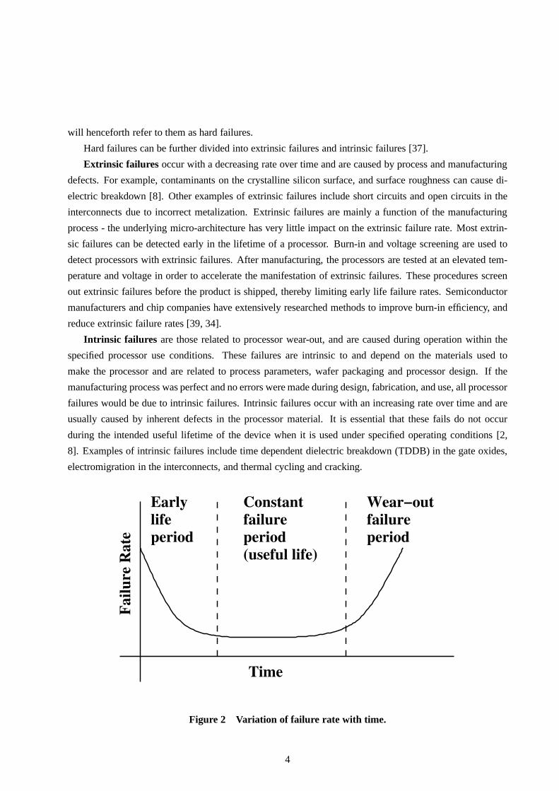
Hard failures can be further divided into extrinsic failures and intrinsic failures [37].
Extrinsic failures occur with a decreasing rate over time and are caused by process and manufacturing
defects. For example, contaminants on the crystalline silicon surface, and surface roughness can cause di-
electric breakdown [8]. Other examples of extrinsic failures include short circuits and open circuits in the
interconnects due to incorrect metalization. Extrinsic failures are mainly a function of the manufacturing
process - the underlying micro-architecture has very little impact on the extrinsic failure rate. Most extrin-
sic failures can be detected early in the lifetime of a processor. Burn-in and voltage screening are used to
detect processors with extrinsic failures. After manufacturing, the processors are tested at an elevated tem-
perature and voltage in order to accelerate the manifestation of extrinsic failures. These procedures screen
out extrinsic failures before the product is shipped, thereby limiting early life failure rates. Semiconductor
manufacturers and chip companies have extensively researched methods to improve burn-in efficiency, and
reduce extrinsic failure rates [39, 34].
Intrinsic failures are those related to processor wear-out, and are caused during operation within the
specified processor use conditions. These failures are intrinsic to and depend on the materials used to
make the processor and are related to process parameters, wafer packaging and processor design. If the
manufacturing process was perfect and no errors were made during design, fabrication, and use, all processor
failures would be due to intrinsic failures. Intrinsic failures occur with an increasing rate over time and are
usually caused by inherent defects in the processor material. It is essential that these fails do not occur
during the intended useful lifetime of the device when it is used under specified operating conditions [2,
8]. Examples of intrinsic failures include time dependent dielectric breakdown (TDDB) in the gate oxides,
electromigration in the interconnects, and thermal cycling and cracking.
Constant
failure
period
(useful life)
Early
life
period
Wear−out
failure
period
Fa
ilu
re R
ate
Time
Figure 2 Variation of failure rate with time.
4

Processor long-term reliability as dictated by the hard failure rate can be depicted by the Bathtub Curve
shown in Figure 2 [32]. This curve shows the failure rate of processors due to hard failures with time.
Loosely, the failure rate at timet, Z(t), can be defined as the probability that a unit will fail at timet after
having survived till timet. A more detailed explanation of failure rate and other reliability definitions can
be found in Appendix B.
The Bathtub curve in Figure 2 is made up of three individual curves related to infant mortality (early
life), useful life, and wear-out. Each region is characterized separately by different failure mechanisms. The
early life failures are due to extrinsic failures and as a result, are process and manufacturing defect related.
As previously discussed, these reduce with time. The usefullife failures are due to random failures that
can occur for a variety of reasons. However, random failurestend to be very rare and the failure rate in
the useful life region can be characterized by a constant value near zero. The wear-out failures are due
to intrinsic failures and are due to inherent material limitations. As previously discussed, these increase
with time. Burn-in and voltage screening attempt to filter out all processors which manifest early-life or
extrinsic failures, and random failures are very low in number 2. As a result, since long-term processor
reliability or lifetime is almost completely dependent on wear-out or intrinsic failures, RAMP only
models intrinsic processor failures. However, it should be noted that RAMP can be extended to model
other types of errors like soft errors.
1.2 Relationship between Processor Temperature and Long-Term Reliability
Processor reliability is directly related to the operatingtemperature and it is expected that many reliability
problems are going to arise because of elevated processor temperatures. The relationship between reliability
and failure is typically given by the well known Arrhenius relationship which is derived from the observed
dependence on chemical reaction rates on temperature changes [5].
Assuming all other parameters are constant, the lifetime ofa processor due to a failure mechanism,
Tfailure is given by [5]:
Tfailure ∝ eEa
kT (1)
whereEa is the activation energy of the failure mechanism in electron volts (eV),k is Boltzmann’s
constant (8.62 × 10⁻⁵ ev/K), andT is the operating temperature.Ea will vary depending on the exact
failure mechanism modeled. It is important to note that thisonly models the temperature dependence of
failure mechanisms and is valid only when all other parameters are constant. It is also possible that some
failure mechanisms do not depend on temperature.
The Arrhenius model tells us that processor lifetime decreases exponentially with temperature. Temper-
ature effects are integrally related to processor reliability. For example, hot-spots on the processor will result
in a higher rate of failure at those sections of the processor. As a result, it is important to accurately model
2Some early life failures can be intrinsic . Burn-in and voltage screening should detect these failures also. However, since earlylife intrinsic failures are very rare, burn-in mainly attempts to capture extrinsic failures.
5

the impact of temperature on long-term reliability of processors. The problems due to increasing tempera-
ture are further compounded by the exponential relationship between leakage power and temperature. As
a result, an important aspect of RAMP’s design is its abilityto model the impact of temperature on failure
mechanisms.
2 Intrinsic Failure Mechanisms and Models
With increase in die size and transistor scaling, failure rates in semiconductor devices are magnified due to
the following:
• Increasing electric field stress- Since supply voltage is not scaling appropriately with technology,
the magnitude of the electric fields on chip are increasing leading to larger stresses. This is particularly
a problem with gate dielectrics.
• Increasing current density - As mentioned previously, higher current densities in the interconnect
lead to faster interconnect wear-out.
• Increasing thermo-mechanical stress- The uneven thermal expansion rates of different materialson
chip causes mechanical stresses which lead to wear-out. This problem is magnified by higher operat-
ing temperatures and the introduction of new dielectric materials which are porous and consequently
brittle in nature [19].
• Multilayer wiring - Multilayer wiring (multiple interconnect layers) leads to higher power densities
in the interconnects leading to higher temperatures. The probability of inter-layer short circuits also
increases.
In this section, we discuss the main wear-out based intrinsic failure mechanisms experienced by pro-
cessors. We also discuss the analytical models for each mechanism as used in RAMP. EM, SM, TDDB,
and TC are currently the only failure mechanisms RAMP models. Our discussions with semiconductor
researchers indicates that these are the main reliability issues faced by processors in the future. However,
due to the modular nature of RAMP, failure models for other mechanisms like Hot carrier injection (HCI),
Negative-bias temperature inversion (NBTI), Corrosion and other failure mechanisms can be easily added.
The metric used to evaluate reliability in RAMP is Mean Time To Failure(MTTF). The MTTF can be
thought of as the average expected lifetime of the processor. RAMP assumes all failure mechanisms have
constant failure rates in order to calculate MTTF. This assumption is clearly inaccurate (a typical wear-out
mechanism, as depicted in Figure 2, will have a very small failure rate for a long time after which the
failure rate will grow rapidly (not including infant mortality)) - however, this assumption allows RAMP to
combine different failure mechanisms and give a unified MTTF. As a result, it is important to understand
that, currently, RAMP does not model reliability as a function of time. RAMP can be used to compare the
reliability of different architectures and applications,only in terms of their MTTF, and not in terms of time.
We are currently working on modeling reliabilty as a function of time in RAMP.
6

Now, if a constant failure rate is assumed, then the MTTF is the inverse of the failure rate. The standard
method of reporting failure rates for semiconductor components is in Failures in Time (FITs) [32], which is
the number of failures per109 device hours. Hence, if the FIT rate is a constant,λ, then the MTTF in hours
is given by:
MTTF =1
λ(2)
Appendix B derives the above expression and discusses reliability metrics and their relationships in more
detail.
2.1 Electromigration
Electromigration is one of the best studied and well understood failure mechanisms in semiconductor de-
vices. Extensive research has been performed by the material science and semiconductor community on
modeling and mitigating the effects of electromigration [29, 5, 4, 31, 3, 17, 15, 18, 13].
Electromigration in aluminum and copper is mainly due to themass transport of conductor metal atoms
in the interconnects due to momentum transferred by the electron current. Conducting electrons transfer
some of their momentum to the metal atoms of the interconnect- this ”electron wind” driving force creates
a net flow of metal atoms in the direction of electron flow. As the atoms migrate, there is depletion of metal
atoms in one region and pile up in other regions. This can leadto the formation and growth of voids at sites
of depletion leading to open circuits, increased interconnect resistance, and other problems. At the site of
pile up, extrusions can form causing shorts between adjacent metal lines causing circuit failure.
2.1.1 Model
The currently accepted model for MTTF due to electromigration (MTTFEM ) is based on Black’s original
electromigration equation [29], and is as follows [5, 15]:
MTTFEM = AEM (J − Jcrit)−ne
Ea
kT (3)
whereAEM is an empirically determined constant,J is the current density in the interconnect,Jcrit is
the critical current density required for electromigration, Ea is the activation energy for electromigration,k
is Boltzmann’s constant,T is absolute temperature in Kelvin, andn is an empirical constant, the value of
which depends on the interconnect material and ranges from 1to 2 [15, 4, 5]. Currently, RAMP uses a value
of 1.1 for copper interconnects. The value ofEa will depend on the material used in the interconnect and is
a parameter that must be set in RAMP. This is further discussed in Section 4.2.J tends to be much higher
thanJcrit in interconnects (nearly 2 orders of magnitude [3]). Hence,(J − Jcrit) ≈ J .
The current density,J , of a line can be related to the switching probability of the line,p, as [18]
J =CVdd
WH× f × p (4)
whereC,W , andH are the capacitance, width, and thickness, respectively ofthe line andf is the clock
frequency.
7

Equations 3 and 4 offer a convenient abstraction for computer architects to work with electromigration.
Abstracting out only the architectural variables for a given process, the MTTF due to electromigration as
modeled in RAMP is given as:
MTTFEM ∝e
Ea
kT
V nfnpn(5)
The above equation is valid for a given process technology.C, W , andH can also be changed to examine
the impact of process scaling on interconnect reliability.
RAMP can further be modified to reflect the type of interconnect by varying the capacitance, width,
thickness and activity of the wires - for example, a power or ground line will have a larger width and
thickness than a signal line. Similarly, a signal line, which has bidirectional current flow will have a lower
average current density than a power line which only has unidirectional current flow [15]. RAMP does not
currently differentiate between different types of interconnects.
Finally, we discuss modeling the impact of scaling on electromigration reliability in Appendix A.1.
2.2 Stress migration
Stress migration is very similar to electromigration. Stress migration is a phenomena where the metal atoms
in the interconnects migrate due to mechanical stress. Stress migration is caused by intrinsic stresses which
are caused by distortions in the crystal lattice of the semiconductor substrate and by thermo-mechanical
stresses which are caused by differing thermal expansion rates of different materials in the device [5, 4].
The exact mechanisms behind stress migration are still not completely understood and research is ongoing
on the subject.
2.2.1 Model
The model for stress migration is based on thermo-mechanical stresses. As mentioned, these stresses are
caused due to the differing thermal expansion rates of different materials in the device. The mechanical
stress due to the different expansion rates,σ, is proportional to the change in temperature . The change in
temperature is measured with respect to the stress free temperature of the metal. The stress free temperature
is the metal deposition temperature - in other words, when the metal was originally deposited on the device,
there were no thermal stresses. However, at any temperaturedifferent from the metal deposition temperature,
there are thermo-mechanical stresses. The mean time to failure due to stress migration,MTTFSM , is given
by [5]:
MTTFSM = ASMσ−neEa
kT (6)
whereσ is the mechanical stress caused due to differing expansion rates,ASM is an empirically de-
termined constant,n is an empirically determined constant ranging in value between 2 and 3 [5, 4], and
Ea is the activation energy for stress migration. The value ofEa will depend on the material used in the
interconnect and is a parameter that must be set in RAMP. Thisis further discussed in Section 4.2.
As mentioned previously, the mechanical stress,σ, is proportional to the change in temperature from the
stress free temperature of the metal - i.e.,σ ∝ |T0 − T | whereT0 is the stress free temperature of the metal
8

(metal deposition temperature), andT is the operating temperature. Abstracting out only the architectural
parameters from Equation 6, the MTTF due to stress migrationas modeled in RAMP is given as:
MTTFSM ∝ |T0 − T |−2.5eEa
kT (7)
The relationship between stress migration and temperatureis governed by two different properties - the
Arrhenius relationship accelerates wear-out with increases in temperature. However, since metal deposition
temperatures tend to be higher than typical operating temperatures3, higher operating temperatures decrease
the value ofT0 −T , thus reducing the value ofσ and increasing the MTTF. However, this increase in MTTF
is typically much smaller than the decrease due to the Arrhenius relationship.
Finally, we discuss modeling the impact of scaling on stressmigration reliability in Appendix A.2.
2.3 Time-dependent dielectric breakdown (TDDB)
Time-dependent dielectric breakdown is an extremely important failure mechanism in semiconductor de-
vices. With time, the gate dielectric wears down with time and fails when a conductive path forms in the
dielectric. When a conducting path forms between the gate and the substrate, it is no longer possible to
control current flow between the drain and the source with a gate electric field, effectively rendering the
transistor device useless [5, 8, 2, 16, 48, 47, 27].
In order to maintain high gate oxide reliability, extreme care is taken during oxide growth in order to
ensure no external impurities are embedded in the oxide. In the past, gate-oxide breakdown was more an
extrinsic failure problem than an intrinsic reliability problem. The intrinsic breakdown reliability of the gate
oxide had been excellent. However, in the past 10 years, due to the advent of thin and ultra-thin gate oxides,
intrinsic gate oxide failure is becoming increasingly important. The failure rate is also increasing due to the
fact that the supply voltage is not scaling down appropriately with technology [16].
2.3.1 Model
Gate oxide reliability depends on temperature, the voltageapplied at the gate, and the electric field at the
gate. It is thought that the temperature degradation of gate-oxide reliability follows a greater than Arrhenius
relationship [48, 47, 27]. Various models have been proposed for TDDB degradation relating TDDB degra-
dation to the electric field, the inverse of the electric fieldand the gate voltage. The TDDB model used in
RAMP is taken from work done by Wu et al. [48, 47] from IBM who have done extensive analytical and
experimental work on TDDB. Wu et al. collected experimentaldata over a wide range of oxide thicknesses,
voltages, and temperatures to create a unified TDDB breakdown model for current and future ultra-thin gate
oxides. The model proposed by Wu et al. [47] shows that the lifetime due to TDDB for ultra-thin gate oxides
is dependent on voltage and has a larger than exponential degradation due to temperature.
3This depends on whether vapor deposition or sputtering was used for depositing the metal - sputtering uses high temperaturesto increase the stickiness of the deposited metal; on the other hand, vapor deposition happens near room temperature [21]
9

The mean time to failure due to TDDB is given by [47]
MTTFTDDB = TBD0e( a
T+ b
T2 ) (8)
whereTBD0, a, andb are determined empirically. In order to be compatible with the conventional Arrhe-
nius temperature dependence with an activation energy, thenon-Arrhenius relationship (e( a
T+ b
T2 )) can be
represented in the form,eEa
kT , whereEa = A + BT
+ CT . Based on [47],A = 0.759ev, B = −66.8evK,
andC = −8.37e − 4eV/K. Hence , the model currently used in RAMP for TDDB is of the form:
MTTFTDDB ∝ e(0.759− 66.8
T−8.37e−5T )
kT (9)
Finally, we discuss modeling the impact of scaling on gate oxide reliability in Appendix A.3.
2.4 Temperature cycling and thermal shock
Fatigue failures can occur in semiconductor due to temperature cycling and thermal shock. Permanent dam-
age accumulates every time there is a cycle in temperature eventually leading to failure. Normal powering
up and powering down will also cause damage. Failures due to temperature cycles can occur in all parts of
the semiconductor device including the silicon substrate,the interconnects, the interlevel dielectrics, and at
die interfaces like solder joints [5, 26]. The problems due to temperature cycling are exacerbated with the
introduction of low-k dielectrics which have higher coefficients of expansion, and are more brittle [19].
Although all parts of the device experience fatigue due to thermal cycling, the effect is most pronounced
in the package and die interface (for example, solder joints). Experiments have shown that very large
thermal cycles of magnitude greater than 140 degrees Celsius are required to cause any damage to the
silicon substrate and interconnects. For smaller thermal cycles, the interconnect and silicon experience
elastic expansion and contraction, and long term damage does not accumulate. As a result, normal use
conditions, including powering up and powering down are notexpected to cause reliability problems in the
silicon and interconnects [40]. Hence, we only model the impact of thermal cycling on the package.
2.4.1 Model
The package goes through two types of thermal cycles - large thermal cycles when the processor is powered
up and down (this includes going into standby and hibernation for mobile processors) which occur at a low
frequency (a few times a day), and small cycles which occur during the course of processor operation which
occur at a much higher frequency (a few times a second).
The effect of small thermal cycles at high frequencies has not been well studied by the packaging com-
munity, and validated models are not available. As a result,RAMP does not currently model the reliability
impact of small thermal cycles.
Large thermal cycles are modeled using the Coffin-Manson equation, which was originally developed for
ductile materials like aircraft frames and has been alteredfor use in semiconductor device reliability. Many
10

different materials and packaging groups have found that the Coffin-Manson equation models semiconductor
reliability well [26]. The Coffin-Manson equation for thermal cycling is [5]:
Nf = C0(δT )−q (10)
whereNf is the number of thermal cycles to failure,C0 is an empirically determined material-dependent
constant,δT is the temperature range experienced in the thermal cycle, andq is the Coffin-Manson exponent,
an empirically determined constant. An alternate way to look at the mean time to failure due to thermal
cycles (MTTFTC) is:
MTTFTC ∝1
fcyclesδT−q (11)
wherefcycles is the frequency of occurrence of the thermal cycle of magnitudeδT . Since we’re only con-
sidering power up and power down cycles, the frequency of thermal cycling is not expected to change with
different architectures and applications. Hence, the model used in RAMP is of the form:
MTTFTC ∝ (δTnominal
Taverage − Tambient
)−q (12)
whereδTnominal is the nominal thermal cycle for which the processor has beenqualified,Taverage −
Tambient is the actual average thermal cycle a structure on chip experiences.
We do not model the reliability impact of the rate of change oftemperature (i.e., we only calculate the
magnitude of the thermal cycle and the frequency of thermal cycling. We do differentiate between a fast
temperature rise and a slow temperature rise.). Experiments have shown that only the number of cycles and
not the rate of change of temperature impact reliability [40].
Finally, we discuss modeling the impact of scaling on thermal cycling reliability in Appendix A.4.
3 Reliability Model
In order to determine the reliability (mean time to failure)of the entire system, we use the sum-of-failure-
rates model. The sum-of-failure-rates has been accepted bythe semiconductor industry as the de-facto
standard for reliability measurement because it offers more knowledge than other methods about the exact
reasons why devices fail.
As mentioned in Section 2, we assume that all the failure mechanisms have constant failure rates. The
exact form of some of the equations that follow are based on this assumption.
3.1 Sum-of-failure-rates (SOFR) model [1]
From a micro-architectural perspective, we treat each structure on chip (branch predictor, instruction win-
dow, etc.) as a separate component. We then assume that each component can fail in different ways, each
of the different ways corresponding to a different failure mechanism (electromigration, TDDB, etc.). The
SOFR model consists of the Competing risk model which estimates the failure rate of each component and
11

the series model which estimates the failure rate of the system based on each component’s failure rates. All
the models are very similar in nature.
Now, to calculate the failure rate of a component using the competing risk model, we make the following
assumptions:
• Each failure mechanism proceeds independently of every other one, at least until a failure occurs.
• The component fails when the first of all the competing failure mechanisms reaches a failure state.
• Each of the failure mechanisms has a known life distributionmodel.
If there are k failure mechanisms, and the failure rate of thecomponent due to theith failure mechanism
is hi(t), then the failure rate of the component due to all failure mechanisms,hc(t) is simply given by:
hc(t) =k∑
i=1
hi(t) (13)
In other words, each failure mechanism acts independently of every other mechanism and the first mech-
anism to reach failure causes the component to fail. Under these conditions, the component reliability is the
product of the failure mechanism reliabilities and the component failure rate is just the sum of the failure
mechanism failure rates. The standard way of reporting failure rates (hc(t)) for semiconductor components
is in Failures in Time (FITs) [32] which is the number of failures per109 device-hours. If we assume that a
component,c, has a constant failure rate ofλ FITs, then mean time to failure for that component,in hours,
MTTFc, is given by:
MTTFc =1
λc=
1∑ki=1 λi
(14)
again, whereλc are the failures in time for the component consisting ofλi for each failure mechanism.
(Appendix B discusses reliability metrics and the relationbetween reliability metrics in more detail.)
The series model is used to build up from components to systems - in this case, the processor. The
assumptions and formulas for the series failure model are identical to the competing risk model. If there are
j components in the system, if we assume each component fails independently of every other component,
and the system fails when the first component fails, then the mean time to failure of the system,MTTFs
depends on each of thej components as follows:
MTTFs =1∑j
i=11
MTTFi
=1∑j
i=1 λi
(15)
MTTFs =1∑j
i=1
∑kl=1 λil
(16)
Equation 15 tells us that the mean time to failure of the system depends on the failure rate of each
component whereλi is the failure rate of theith component. This leads to Equation 16 which shows that the
mean time to failure of the processor is the inverse on the sumof the failure rates of all failure mechanisms
for all components whereλil is the failure rate of theith component due to thelth failure mechanism.
12

Equation 16 can be altered to account for redundant structures and non-critical structures (for example, if
the branch predictor was not working correctly, the processor could possibly continue to function, although
it would keep making prediction mistakes) by adding weights:
MTTFs =1∑j
i=1
∑kl=1 Wil ∗ λil
(17)
whereWil is the weight of componenti and failure mechanisml. The weight is a value between 0 and
1 (depending on redundancy and criticality of the component), and the default value is 1.
Given the failure rates for different mechanisms at a particular voltage, frequency, and temperature,
we can use the above expression to directly determine MTTF for a processor under a range of different
circumstances. We can also factor in other parameters like switching activity (for electromigration). We can
calculate each architectural structure’s failure rates based on local temperature measurements and even local
voltage and frequency measurements (for multiple voltage and frequency domain processors).
RAMP calculates the system FIT rate every sampling intervaland maintains an average FIT rate for
the entire simulation run. The average MTTF of the benchmarkis then the inverse of the average FIT
rate. Similarly, the average MTTF for a given workload (which can consist of many benchmarks) is the
inverse of the the average FIT rate for all the benchmarks. Since RAMP maintains FIT rates continuously
for every structure for every failure mechanism, the MTTF ofindividual structures due to individual failure
mechanisms can also be determined.
3.2 Initialization
RAMP has to be initialized with FIT rates for each structure due to each failure mechanism at some fixed
voltage, frequency and temperature. Based on these initialvalues and using the MTTF models, RAMP cal-
culates relative FIT rates (FITs are inversely proportional to MTTF) for each structure for each mechanism.
The default mode in RAMP assumes that the initial FIT rate foreach structure is proportional to its area.
However, individual initial values can be set.
RAMP also has to be initialized with base activity factors for each structure for the electromigration
model. Based on these activity factors, RAMP calculates relative activity factors. Currently RAMP uses the
average activity factors over the SPEC2k benchmark suite asthe base activity factor. This can be changed if
required.
3.3 Temperature measurement
Accurate temperature estimation at the granularity of eachmicro-architectural structure is essential to the
accuracy of the reliability model.Reliability calculations are done at the same time and space granularity as
temperature measurement.
13

3.4 Leakage power
Leakage power measurement is also extremely important to the reliability model. The exponential nature of
leakage current with temperature causes the power dissipation of processors to increase with temperature.
This increase in power consumption leads to further rises intemperature. This positive feedback loop can
lead to thermal runaway. Because most failure mechanisms depend on temperature, modeling leakage power
is essential to the accuracy of the reliability model.
3.5 Cost model
One interesting option is to add a cost model into RAMP. This can be useful in examining reliability cost
tradeoffs. For example, the cost and reliability of a serverclass processor and the cost and reliability of a low
end processor. This might be particularly useful because itgives a more realistic way to look at reliability.
4 Using RAMP
The RAMP simulation model is a self standing module written in C++ which can be integrated with an
architectural simulator tool. As mentioned previously, the architectural simulator should have power and
temperature models attached. Currently, RAMP has been integrated with two different simulators: IBM’s
Turandot architectural simulator [35] which has its own power model and which uses HotSpot [43] for
temperature simulation, and the RSIM simulator [24] which uses Wattch [11] for power measurements and
HotSpot [43] for temperature measurements. Both simulators also have a temperature dependent leakage
model. Because RAMP is a separate module with its own interface, it should be fairly easy to port to other
simulators.
RAMP provides failure rates and lifetimes for specific applications when they are simulated on the
architectural simulator. It is important to note that reliability is inherently statistical in nature and that
there is no significance in reliability estimates at specificinstances of time. The average FIT rate over the
entire run of an application, or the average FIT rate for all the applications which will be typically run on a
processor will have to be used to gain insight on processor reliability.
4.1 Using RAMP Within an Architecture Simulator
There are two main files in the RAMP software - the reliabilityfunctions are inreliability.cc and
the simulator parameters are inreliability.h. TheUnitRel class contains the reliability models,
and during initialization, aUnitRel object should be created for every structure on chip. The functions
UnitRel::init()andUnitRel::fitinit()are used to initialize RAMP parameters and FIT rates
for each structure. During simulation, the functionUnitRel::allmodels(temperature, activ-
ity factor, voltage, frequency) is called for each structure at an appropriate granularity.The
UnitRel::allmodels() function invokes the individual reliability models for each failure mechanism.
14

As mentioned previously, additional failure mechanisms can be modeled and added toreliability.cc
.
4.2 RAMP Parameters
RAMP is currently configured with parameters which are basedon current and near future processors.
However, these parameters can be altered inreliability.h.
• TOTAL EM FITS: Total number of FITS over the entire processor due to EM initially at initialization.
This is the base value obtained from chip wide MTTF numbers.
• TOTAL SM FITS: Total number of FITS over the entire processor due to SM initially at initialization..
This is the base value obtained from chip wide MTTF numbers.
• TOTAL TDDB FITS: Total number of FITS over the entire processor due to TDDB initially at ini-
tialization. This is the base value obtained from chip wide MTTF numbers.
• TOTAL TC FITS: Total number of FITS over the entire processor due to TC initially at initialization.
This is the base value obtained from chip wide MTTF numbers.
The above 4 parameters can be changed to reflect the specifics of different chips. Also, the initial FIT
rate is distributed over the chip based on structure area. This can be also be altered.
• T base: Base temperature at which initialization FITS are measured. The FIT rate at any other
temperature is calculated with respect to this value.
• VDD base: Base voltage at which initialization FITS are measured. The FIT rate at any other voltage
is calculated with respect to this value.
• freq base: Base frequency at which initialization FITS are measured.The FIT rate at any other
frequency is calculated with respect to this value.
• EM Ea div k: The EM activation energy divided by Boltzmann’s constant.The default setting as-
sumes the interconnects are copper based andEa is 0.9 ev. If the interconnects are copper-aluminum
alloys, theEa will be lower. [5, 4]
• SM Ea div k: The SM activation energy divided by Boltzmann’s constant.The default setting is the
same asEM Ea div k [5, 4].
• SM T base: The stress free temperature of the interconnect metal for SM (the vapor deposition
metal). The default value is 500K [21].
• TC q: The TC exponent - The value for ductile metal like solder ranges from 1 to 3. The value for
interconnect metals ranges from 3 to 5, and the value for the silicon substrate and dielectrics ranges
from 6 to 9. Currently, RAMP only tracks reliability of the package and assumes the value is 1.9 [5].
15

• TC base temp diff: Thermal cycle the system goes through during power up and power down.
This is usually the only reliability metric available for processor thermal cycling. We compare all
thermal cycles with this value. Default is 80 degrees.
5 Conclusions
RAMP provides an architectural model for long-term reliability measurement. Its most important features
are the inclusion of temperature, voltage, activity factors, and frequency in reliability calculations and it’s
separation of architectural structures and failure mechanisms. As a result, the failure rate of individual
structures on chip due to individual failure mechanisms canbe studied.
With decreasing transistor dimensions and increasing processor power and temperature, reliability due
to wear-out mechanisms is expected to become a significant issue in microprocessor design and reliability
awareness at the micro-architectural design stage will soon be a necessity. RAMP provides a convenient
way to look at microprocessor long-time reliability and theimplications of running different applications,
architectural features, and processor design on reliability.
RAMP is a self-standing module which can be attached to architectural simulators which generate power
and temperature measurements. It is currently running on IBM’s Turandot processor simulator and the RSIM
architectural simulator and can easily be ported to other simulators.
RAMP does not currently model soft errors in processors and this is viewed as an area for future work.
Additional failure models for failure mechanisms like hot-carrier injection and NBTI should also be added.
A Modeling the Impact of Scaling on Reliability
Since scaling limits are fast approaching due to reliability concerns, the impact of scaling on reliability
should be evaluated at all stages of microprocessor design,including the microarchitectural definition phase.
In this appendix, we discuss modeling the impact of scaling on the various failure mechanisms in RAMP.
A.1 Electromigration
For years, copper doped aluminum had been the semiconductorindustry’s interconnect metal of choice
because of its ease of integration into the manufacturing process, low resistivity, and cheap availability.
In the past few years, reliability problems due to electromigration and a need for even lower resisitivities
prompted the industry to consider using only copper for interconnects. Copper has lower resistivity (and
hence lower interconnect delay) than copper doped aluminumand is much more resilient to electromigration
(Experimental results by Hu et al. [13] show that the electromigration lifetime of copper interconnects is 50
to 1000 times as high as copper doped aluminum interconnects). However, there are problems with using
copper - in particular, copper diffuses readily into silicon causing deep level defects. This problem is solved
by adding a lining layer using tantalum (Ta) which separatesthe copper interconnects from the surrounding
devices [30].
16

Figure 3 Electromigration in copper interconnects.
Copper interconnects have now moved from development to manufacturing and high-level server proces-
sors already use copper interconnects [46]. Some commodityprocessors have also started using all copper
interconnects and the rest are expected to start using copper interconnects in the near future.
The impact of scaling on electromigration reliability is different for copper and aluminum interconnects.
This is because of the difference in the electromigration mechanism between copper and aluminum. In
copper, electromigration is interface dominated [13]. Electromigration in aluminum, on the other hand, is
grain boundary dominated [23]. Since it is expected that copper will be the dominant interconnect metal in
the future, we only model the impact of scaling on copper interconnects in RAMP.
Copper interconnections are typically fabricated using a damascene processing method. In these struc-
tures, the top surface of the copper damascene line is covered with a dielectric filem, while the bottom
surface and two sidewalls are sealed with a tantalum (Ta) liner [20]. The tantalum liner prevents electromi-
gration along the surfaces it covers. However, the top surface of the line can not be covered with tantalum
due to manufacturing constraints. As a result, electromigration in copper is dominant at the top interface
layer between the interconnect and the dielectric [14]. This is illustrated in Figure 3.
If the effective thickness of the interface layer isδ, and the interconnect width isw, then the electro-
migration flux is constrained to an areaδw. If the height of the interconnect ish, then the interconnect
current flows through an areawh. The relative amount of atomic flux flowing through the interface region
is proportional to the interface area to interconnect area ratio δwwh
= δh
.
Electromigration voids are found to occur most commonly at the interface between the interconnects
and the metal vias [13]. Although large vias are favorable from a reliability perspective, large vias incur
area overheads and the interconnect density is reduced. As aresult, the width of the via is kept the same
as the width of the interconnect,w. Electromigration failure is considered to have occurred when the void
formed grows larger than the width of the via,w (in that case, there is no path to conduction between the
17

void and the interconnect other than the liner, and hence, resistance goes up causing circuit failure). Time to
failure due to electromigration,τ , is then proportional to the width of the via,w, and inversely proportional
to the relative amount of flux passing through the interface region, δh
[13].
τ ∝ (w ×h
δ) (18)
When a scaling constant,κ, is applied to Equation 18, it can be seen that the electromigration lifetime
reduces byκ2 with scaling (bothw andh scale byκ while δ remains constant). This assumes constant
current density is maintained with scaling [13]. Although the wire dimensions are reduced, designers ensure
that the current density remains constant in order to keep electromigration effects under control. If current
density also increases with scaling, then electromigration lifetime will scale by a factor much larger thanκ2.
Hence, electromigration lifetime with respect to scaling can be expressed as:
MTTFEM ∝ (J)−1.1eEa
kT wh (19)
whereJ is the current density and is assumed to be constant with scaling. If J does not remain constant,
that should also be factored into Equation 19. Maintaining constantJ with scaling is becoming increasingly
difficult and it is expected that the value ofJ will begin to increase, reducing lifetime. MTTF due to
electromigration is reduced further due to the higher temperatures seen with scaling.
A.2 Stress Migration
The only impact of scaling on stress migration that is modeled in RAMP is the Arrhenius temperature
relationship. Scaling has no other direct impact on stress migration.
However, there are some indirect effects due to scaling. Scaling requires the increased use of low-
k dielectrics for the inter-level dielectric layers. Thesematerials tend to be porous, and brittle. Despite
the use of low-k dielectrics by some manufacturers like IBM for their 0.13µm Copper process [46], the
dielectrics are thought to have some reliability problems [22]. The thermal expansion rates of these new
low-k dielectrics also tends to be significantly different from the interconnect thermal expansion rate [22].
A consequence of the different expansion rates and the brittle nature of the dielectrics causes higher failure
rates due to thermo-mechanical stresses in stress migration. We do not account for these indirect scaling
effects currently.
A.3 Time Dependent Dielectric Breakdown (TDDB)
Scaling has a profound effect on gate oxide reliability. Much work has been done on estimating and increas-
ing gate oxide reliability. As mentioned previously, the supply voltage is not scaling at the same rate as gate
oxide thickness. This will result in a significant drop in gate oxide reliability with scaling.
The fundamental physical limitations caused by gate oxide thickness are related to the exponentially
increasing gate current and its implications for device performance and reliability. With ultra thin oxides
with tox less than 4nm, gate tunneling current is also increasing. This gate leakage current increases power
18

consumption and imposes a practical bound on oxide thickness [27]. The increase in gate leakage current
not only affects power consumption but accelerates wear-out due to TDDB.
Since time to break down,tBD, is based on total required charge to breakdown,QBD, tBD ∝ 1I
where
I is gate leakage current (QBD = IBDtBD). The gate leakage current increases by one order of magnitude
for every 0.22nm reduction in gate oxide thickness [27, 33].As a result, if gate oxide thickness reduces
by ∆tox with scaling, then time to breakdown,tBD reduces by10∆tox
0.22 , where the reduction in gate oxide
thickness,∆tox, is expressed in nanometers.
Decreasing supply voltage increases reliability. It is generally accepted that a decrease in supply voltage
of 0.2 V increases reliability by a factor of 10 to 100 [28, 33]. A more recent model proposed by Wu et
al. [48, 47] relates voltage and gate oxide time to break downas:
tBD ∝ (1
V)(a−bT ) (20)
where a and b are empirical constants and T is the operating temperature.
Finally, for the current and future range gate oxide thicknesses, the time to breakdown is inversely
proportional to the total gate oxide surface area [27, 48, 47].
Hence, if we scale down from process 1 to process 2, which havegate oxide thicknesses,tox1 andtox2,
and supply voltages,V1 andV2, and total gate oxide areas ofA1 andA2, the ratio of the mean time to
failures,MTTF1 andMTTF2, at temperaturesT1 andT2, is given by:
MTTF1
MTTF2= 10
(tox1−tox2)
0.22 ×V
(a−bT2)2
V(a−bT1)1
×A1
A2×
e
(A+ B
T1+CT1)
kT1
e
(A+ B
T2+CT2)
kT2
(21)
where A, B, C, a and b are empirically determined constants. Based on [47],A = 0.759ev, B =
−66.8evK, C = −8.37e − 4eV/K, a=78 and b=-0.081.
A.4 Thermal Cycling
Like stress migration, the only impact of scaling on thermalcycling modeled in RAMP is the impact of
temperature. Scaling has no other direct impact on thermal cycling. However, the increased device power
densities result in larger swings in temperature which accelerate thermal cycling wear-out.
There are some indirect effects on thermal cycling due to scaling. Fewer thermal cycles are required to
cause failure in low-k dielectrics because of the increasedporosity and brittleness. The adhesive properties
of dielectrics (in particular low-k dielectrics) also degrades with scaling. This impacts thermal cycling
failure rate.
B Reliability Metrics [32, 1]
B.1 Some reliability definitions
• Failure Rate: As mentioned in Section 1, the failure rate at timet, Z(t), can be defined as the
probability that a unit will fail at timet after having survived till timet. An alternate definition of
19

failure rate at timet, is the number of failures per unit time, compared with the number of surviving
components at timet.
• Mean time to failure (MTTF): As mentioned in Section 2, the MTTF can be thought of as the
average expected lifetime of the processor, or in other words, the expected value of the time to failure
of the processor. It is important to understand that this a statistical average and is significant only in
the context of many processors.
• Failures in time (FITS): As mentioned in Section 2, FITs are a standard way of representing failure
rates in semiconductor devices. A FIT is a unit representinga single failure in109 (1 billion) device
operating hours.
In the next definition, we derive the relationships between the above quantities.
B.2 Relationships between failure metrics
If we conduct an aging experiment withN identical components, after a timet, S(t) will still be operating,
andF (t) would have failed. In this case, at any timet, the probability of survival of the components, also
known as the reliability,R(t), is:
R(t) =S(t)
N(22)
The probability of failure of the components, also known as the unreliability,Q(t), is:
Q(t) =F (t)
N(23)
SinceS(t) + F (t) = N , we must haveR(t) + Q(t) = 1.
Based on this, the failure rate of the system,Z(t), defined as the number of failures per unit time,
compared with the number of surviving components, is:
Z(t) =1
S(t)
dF (t)
dt=
1
R(t)
dQ(t)
dt(24)
As mentioned in Section 1, for typical semiconductor devices, the failure rate follows a bathtub curve(Figure 2).
The initial high failure rate section is called the early life period, the middle section is the useful life, and
the final phase is the wear-out phase.
The system reliability,R(t) has different values at different times and varies with operating conditions
like temperature and voltage. This metric is not ideal for practical use. More useful to the user is the average
time to failure, known as the Mean Time To Failure(MTTF). TheMTTF of a system is usually expressed in
hours and is defined as the area under the reliability curve, that is,∫∞
0 R(t)dt.
Failures in Time (FITs) are the number of failures seen per109 (1 billion) device operating hours and is
the standard way of reporting failures for semiconductor devices.
As mentioned previously, RAMP assumes all failure mechanisms have constant failure rates in order to
calculate MTTF. This assumption is made in order to easily combine different failure mechanisms and give
a unified MTTF.
20

Now, if the failure rate of the system is assumed to be a constant, equal toλ FITs, then:
Z(t) = λ (25)
SinceR(t) = 1 − Q(t) andQ(t) = F (t)N
,
R(t) = 1 −F (t)
N(26)
Differentiating,dR(t)
dt= −
1
N
dF (t)
dt(27)
Substituting Equation 27 in Equation 24,
Z(t) = λ = −N
S(t)
dR(t)
dt(28)
SinceR(t) = S(t)N
λ.dt = −dR(t)
R(t)(29)
For a system, at time 0, reliability,R(0) = 1. At time t, the reliability isR(t). Integrating Equation 29,
λ
∫ t
0dt = −
∫ R(t)
1
1
R(t)dR(t) (30)
Substituting the limits,
λ(t − 0) = −| ln R(t) − ln 1| (31)
−λ.t = ln R(t) (32)
Hence, the reliability function for the constant failure rate,λ, is:
R(t) = e−λ.t (33)
Now, sinceMTTF =∫∞
0 R(t)dt,
MTTF =
∫∞
0e−λ.tdt (34)
MTTF = −1
λ|e−λ.t|∞0 =
1
λ(35)
Hence, the relation between MTTF and failure rate boils downto
MTTF =1
λ(36)
21

Figure 4 MTTF goal.
B.3 MTTF goals and requirements
Ensuring long-term reliability is an essential goal for allmicroprocessor manufacturers. The manufacturing
process is required to ensure that all shipped products meeta pre-specified reliability target. Early life
failures are caught during burn-in and voltage screening. All other products that are shipped are expected to
have a MTTF of around 30 years [10]. The MTTF target tends to bemuch larger than the expected lifetime
of consumer use of the product. However, as discussed earlier, physical wear-out mechanisms are governed
by stochastic processes with a distribution of failure times related to some probability function. The choice
of fail time is selected such that the nominal product consumer service life(typically less than 8 years) will
fall far out in the tails of the failure mechanism probability distribution [2]. This is illustrated in Figure 4
which represents a typical semiconductor device failure probability distribution.
B.4 Impact of Burn-in and voltage screening
As discussed previously, burn-in and voltage screening attempt to filter out samples which fall in the early
failure or infant mortality region. Burn-in and voltage screening subject the devices to accelerated wear-out
in the hope of causing early failure devices to fail - however, since all products are subjected to burn-in,
burn-in also has the adverse effect of reducing the effective life of useful devices. Minimizing the effect of
burn-in is the subject of considerable research by the semiconductor industry [39, 34, 2, 5, 4]. The impact
of burn-in and voltage screening is illustrated in Figure 5.
References[1] Assessing Product Reliability, Chapter 8, NIST/SEMATECH e-Handbook of Statistical Methods. In
http://www.itl.nist.gov/div898/handbook/.
22

Figure 5 Impact of Burn-in and voltage screening
[2] Reliability in CMOS IC Design: Physical Failure Mechanisms and their Modeling. InMOSIS Techni-cal Notes, http://www.mosis.org/support/technical-notes.html.
[3] Electromigration for Designers, Ca-dence Design Systems White Paper. Inhttp://www.cadence.com/whitepapers/electromigration.html,1999.
[4] Sony Semiconductor Quality and Reliability Handbook. In Sony Global Corp., 2001.
[5] Failure Mechanisms and Models for Semiconductor Devices. InJEDEC Publication JEP122-A, JedecSolid State Technolgy Association, 2002.
[6] Critical Reliability Challenges for The Internatinonal Technology Roadmap for Semiconductors. InInternational Sematech Technology Transfer Document 03024377A-TR, 2003.
[7] IBM CONFIDENTIAL REPORT: Determination of Experimentsto Verify Effect of Temperature onChip Reliability. InIBM Academy of Technology Workshop, 2003.
[8] W. Abadeer et al. Key Measurements of Ultrathin Gate Dielectric Reliability and In-Line Monitoring.In IBM Journal of Research and Development, 1999.
[9] T. M. Austin. Diva: A reliable substrate for deep submicron microarchitecture design. InProc. of the32nd Annual Intl. Symp. on Microarchitecture, 1998.
[10] D. Bossen. Personal communication. 2003.
[11] D. Brooks, V. Tiwari, and M. Martonosi. Wattch: A Framework for Architectural-Level Power Anal-ysis and Optimizations. InProc. of the 27th Annual Intl. Symp. on Comp. Architecture, 2000.
[12] A. Buyuktosunoglu et al. Energy efficient co-adaptive instruction fetch and issue. InProc. of the 30thAnnual Intl. Symp. on Comp. Architecture, 2003.
[13] C.-K.Hu et al. Scaling effect on electromigration in on-chip cu wiring. In International ElectronDevices Meeting, 1999.
[14] C-K.Hu et al. Comparison of cu electromigration lifetime in cu interconnects coated with various caps.In Applied Physics Letters, August,2003.
23
[15] A. Chandrakasan, W. J. Bowhill, and F. Fox. Design of High-Performance Microprocessor Circuits.2001.
[16] K. P. Cheung. Thin Gate-oxide Reliability - the currentstatus. InKeynote paper, Symposium on NanoDevice Technology 2001, 2001.
[17] A. Christou. Electromigration and Electronic Device Degradation. 1994.
[18] A. Dasgupta and R. Karri. Electromigration Reliability Enhancement Via Bus Activity Distribution.In 33rd Design Automation Conference, 1996.
[19] K. Diefendorff. Ibm paving the way to 0.10 micron. InMicroprocessor Report, May 2000.
[20] D. Edelstein et al. A high performance liner for copper damascene interconnects. InInternationalInterconnect Technology Conference, 2001.
[21] E.Eisenbraun et al. Integration of cvd w- and ta-based lines for copper metallization. InMKS whitepaper, http://www.mksinst.com/techpap.html, 2000.
[22] E.T.Ogawa et al. Leakage, breakdown, and tddb characteristics of porous low-k silica based intercon-nect materials. InInternational Reliability Physics Symposium, 2003.
[23] G.Yoh and F. Najm. A statistical model for electromigration failures. InInternational Symposium onQuality Electronic Design, 2000.
[24] C. J. Hughes, V. S. Pai, P. Ranganathan, and S. V. Adve. RSIM: Simulating Shared-Memory Multi-processors with ILP Processors.IEEE Computer, February 2002.
[25] C. J. Hughes, J. Srinivasan, and S. V. Adve. Saving energy with architectural and frequency adaptationsfor multimedia applications. InProc. of the 34th Annual Intl. Symp. on Microarchitecture, 2001.
[26] H.V.Nguyen et al. Fast temperature cycling stress-induced and electromigration-induced interlayerdielectric cracking failure in multilevel interconnection. 2001.
[27] J.H.Stathis. Reliability limits for the gate insulator in cmos technology. InIBM Journal of Researchand Development, 2002.
[28] J.H.Stathis and D.J.DiMaria. Reliability projections for ultra-thin oxides at low voltage. InInterna-tional Electron Devices Meeting, 1998.
[29] J.R.Black. A brief survey of electromigration and somerecent results. InIEEE Transactions onElectron Devices, 1969.
[30] K.H.Min et al. Comparative study of tantalum and tantalum nitrides as a diffusion barrier for cumetallization. InJournal of Vacuum Science and Technology, 1996.
[31] J. Kitchin and T.S.Sriram. A Statistical Approach to Electromigration Design for High PerformanceVLSI. In Fourth International Workshop on Stress Induced Phenomena in Metallization, 1998.
[32] P. K. Lala. Self-checking and fault-tolerant digital design.
[33] B. Linder. Personal communication. 2003.
[34] N. P. Mencinger. A mechanism-based methodology for processor package reliability assessments. InIntel Technology Journal, Q3,2000.
[35] M. Moudgill, P. Bose, and J. H. Moreno. Validation of turandot, a fast processor model for microarchi-tecture evaluation. InInternational Performance, Computing and Communication Conference, 1999.
[36] D. Patterson et al. Recovery-oriented computing (roc): Motivation, definition, techniques, and casestudies. InUC Berkeley Computer Science Technical Report UCB//SD-02-1175, 2002.
[37] M. G. Pecht et al. Guidebook for Managing Silicon Chip Reliabilty. 1998.
24

[38] E. Rotenberg. Ar/smt: A microarchitectural approach to fault tolerance in microprocessors. InInter-national Symposium on Fault Tolerant Computing, 1998.
[39] K. Seshan et al. The Quality and Reliability of Intel’s Quarter Micron Process. InIntel TechnologyJournal, Q3,1998.
[40] T. M. Shaw. Personal communication. 2003.
[41] P. Shivakumar et al. Modeling the Effect of Technology Trends on the Soft Error Rate of CombinationalLogic. In International Conference on Dependable Systems and Networks, 2002.
[42] P. Shivakumar et al. Exploiting microarchitectural redundancy for defect tolerance. In21st Interna-tional Conference on Computer Design, 2003.
[43] K. Skadron et al. Temperature-Aware Microarchitecture. In Proc. of the 30th Annual Intl. Symp. onComp. Architecture, 2003.
[44] L. Spainhower and T. A. Gregg. Ibm s/390 parallel enterprise server g5 fault tolerance: A historicalperspective. InIBM Journal of Research and Development, September/November 1999.
[45] J. Srinivasan and S. V. Adve. Predictive dynamic thermal management for multimedia applications. InProc. of the 2003 Intl Conf. on Supercomputing, 2003.
[46] T.McPherson et al. 760 mhz g6 s/390 microprocessor exploiting multiple vt and copper interconnects.In ISSCC Digest of Technical Papers, 2000.
[47] E. Y. Wu et al. Interplay of voltage and temperature acceleration of oxide breakdown for ultra-thingate dioxides. InSolid-state Electronics Journal, 2002.
[48] E. Y. Wu et al. Cmos scaling beyond the 100-nm node with silicon-dioxide-based gate dielectrics. InIBM Journal of Research and Development, March/May, 2002.
25