i0222 - consumer solutions brochure - lattice semi
TRANSCRIPT
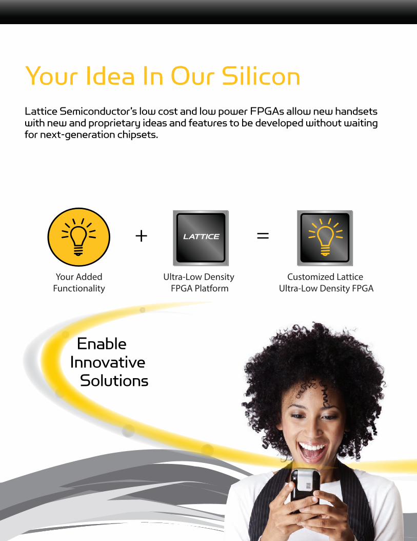
Your AddedFunctionality
+
Customized Lattice Ultra-Low Density FPGA
Ultra-Low Density FPGA Platform
=
Your Idea In Our SiliconLattice Semiconductor’s low cost and low power FPGAs allow new handsets with new and proprietary ideas and features to be developed without waiting for next-generation chipsets.
Enable Innovative Solutions

Your AddedFunctionality
+
Customized Lattice Ultra-Low Density FPGA
Ultra-Low Density FPGA Platform
=
Ultra-Low Density FPGAs Enable DifferentiationUltra-low density FPGAs from Lattice serve as companion chips to standard Application Processors (APs), enabling consumer mobile designers to quickly and easily bring new features and capabilities to market.
Quickly meet new customer demand Stay ahead of the competition Create proprietary solutions Innovate now!
For New Opportunities

4
Table of ContentsSensor Management ..........................................................................................................5 - 13EBI2 to I2C BridgingInterrupt AggregationAuto-PollingSLIMbus to Multiple I2C InterfacesSPI Port ExpansionEnabling “Always-On” Applications in Smartphones Enabling Universal Remote in SmartphonesEnabling “E-Commerce” Applications in SmartphonesTunable Antenna
Video and Imaging ............................................................................................................14 - 22Display Interface ConversionVideo UpscalingVideo XY SwappingImage Mirroring and DownscalingAutostereoscopic 3D Panel TCONCustomized Pattern Detection for 3D GlassColor Space Conversion and TCONVideo in VideoEnabling Dual Display Cameras
Memory and Storage ........................................................................................................23 - 25eMMC Support for ProcessorsSD MemorySmart Frame Buffer
Connectivity ......................................................................................................................26 - 36Keyboard Dock using USB1.1Media Dock with Image Upscaling and Audio MuxingUSB2.0 Host ControllerNokia’s Enhanced Control InterfaceInter-Processor CommunicationSIM SwitchingSD Mux and Resource SharingSPI to UART ExpansionAdding High-end Features to Low Cost PhonesTunable AntennaSLIMbus to I2SMIPI-BIF (Battery Interface) for SmartphonesMultiprocessor Systems

5
Eliminating “Sensor Choke” in Smartphones(EBI2 to I2C Bridging)
Too many I2C devices
Bridge slow I2C devices to a high-speed bus
Smartphones now have as many as 15 to 20 sensors.
All are trying to talk to the processor through a slow I2C port.
This chokes the application processor and kills system performance.
Lattice ultra-low density FPGAs can implement multiple buffered I2C controllers.
Connect them to the application processor through a high-speed parallel bus, (such as EBI2) and high-speed serial bus (such as SPI).

6
Smart Sensor Management for Smartphones(Interrupt Aggregation)
Multiple sensor interrupts slow down smartphone responses
Interrupt aggregator offloads processor and improves performance
Multi-touch screens can generate very heavy interrupts at a given time.
This tremendously increases processor overhead and potentially affects other tasks.
Lattice ultra-low density FPGAs can aggregate multiple sensor interrupts into efficient summaries to offload the processor.
The interface to the processor (red dotted box) can be customized to any available interface such as SPI or a processor local bus’ offering extra flexibility in terms of design integration.

7
Smart Sensor Management for Smartphones (Auto-Polling)
Sensor polling increases processor overhead
Offload processor with built-in auto-polling and data filtering
Some “chatty sensors”, such as gyroscopes, require constant polling from the processor.
This is very troublesome for the processor and often prevents the processor from entering into the sleep state.
Lattice ultra-low density FPGAs can incorporate auto-polling as a feature to offload the processor.
It can further be used to filter out unnecessary data to increase interrupt efficiency.

8
Sensor Expansion and Management via SLIMbus(SLIMbus to Multiple I2C Interfaces)
Increasing sensors, but no good way to connect to processor
Connect multiple sensors through MIPI-SLIMbus
Smartphones have increasing demand for sensors.
Most of these use slow I2C interfaces.
This creates an application processor I2C bottleneck.
Lattice ultra-low density FPGAs can implement a SLIMbus to multiple I2C adapters.
This allows the application processor to use the SLIMbus to manage the sensors.
9
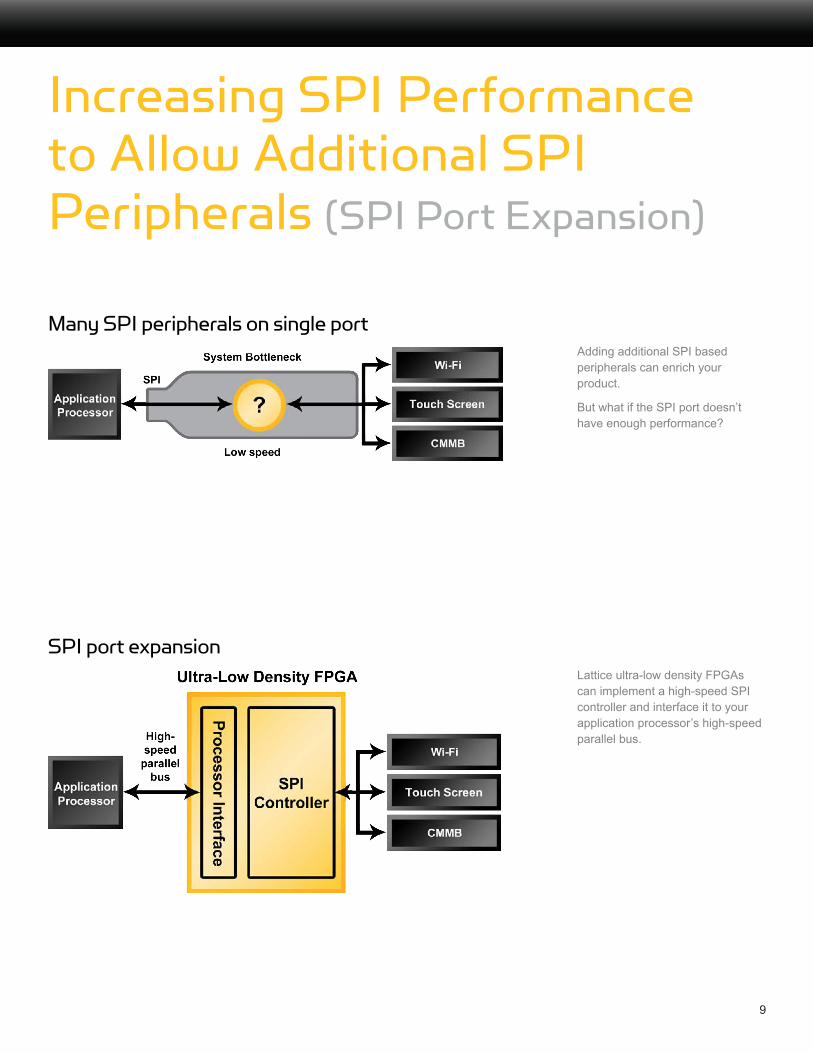
Increasing SPI Performance to Allow Additional SPI Peripherals (SPI Port Expansion)
Many SPI peripherals on single port
SPI port expansion
Adding additional SPI based peripherals can enrich your product.
But what if the SPI port doesn’t have enough performance?
Lattice ultra-low density FPGAs can implement a high-speed SPI controller and interface it to your application processor’s high-speed parallel bus.

10
Enabling “Always-On” Applications in Smartphones(Always-On Pedometer)
Sensor Management chips are too power hungry
Enable “Always-On” applications
Smartphones now have several sensors.
Sensor management chips consume too much power to be used in “always on” modes - e.g. Pedometer.
Lattice ultra-low density FPGAs can be used to create low power “always-on” solutions using the accelerometer.
Implement multiple I2C masters to completely isolate low & high power sensors.
Wake up high power sensors only after determining an event using only the low power accelerometer
Ultra-Low Density FPGA
11
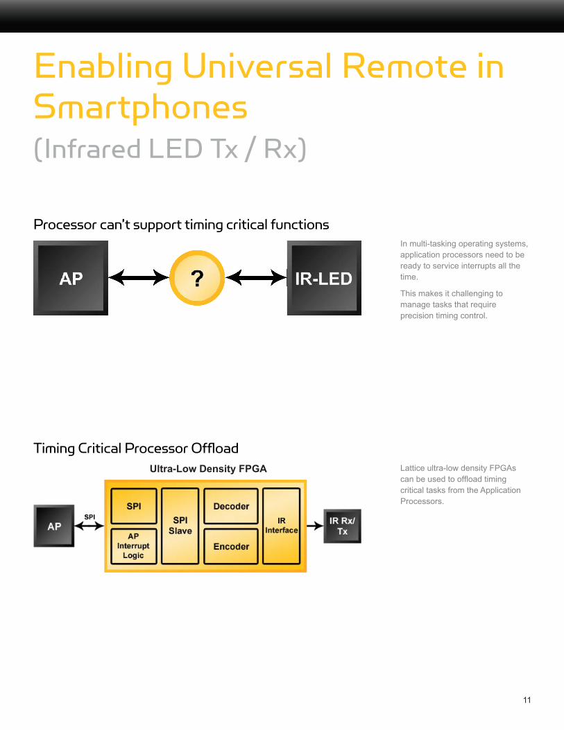
Enabling Universal Remote in Smartphones (Infrared LED Tx / Rx)
Processor can’t support timing critical functions
Timing Critical Processor Offload
In multi-tasking operating systems, application processors need to be ready to service interrupts all the time.
This makes it challenging to manage tasks that require precision timing control.
Lattice ultra-low density FPGAs can be used to offload timing critical tasks from the Application Processors.
Ultra-Low Density FPGA

12
Enabling “E-Commerce” Applications in Smartphones(Barcode Emulation)
LCD Glass too reflective for 1-D barcode readers
Timing Critical Processor Offload
1-D barcodes displayed on the LCD screens are not readable by traditional barcode scanners
Reflections from 1-D barcodes can be emulated using a LED. This requires time critical control of LEDs.
In multi-tasking operating systems, it is not efficient for application processors to control LEDs for barcode emulation.
Lattice ultra-low density FPGAs can be used to offload the timing critical barcode emulation function from the application processor.
13
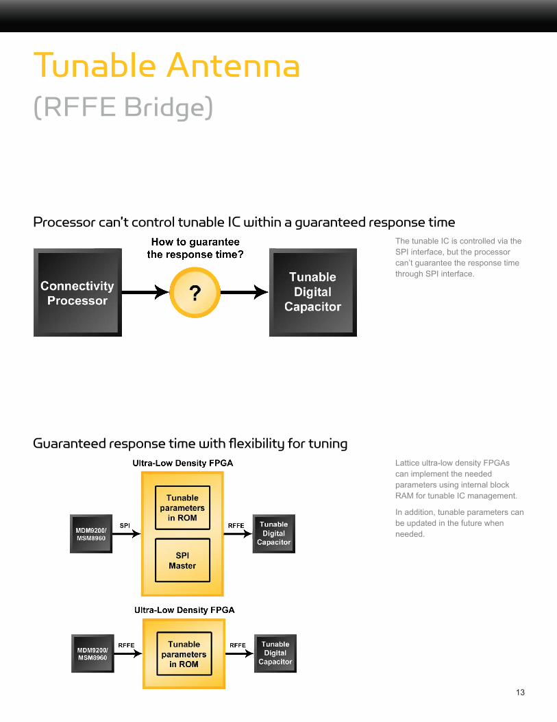
Processor can’t control tunable IC within a guaranteed response time
Guaranteed response time with flexibility for tuning
The tunable IC is controlled via the SPI interface, but the processor can’t guarantee the response time through SPI interface.
Lattice ultra-low density FPGAs can implement the needed parameters using internal block RAM for tunable IC management.
In addition, tunable parameters can be updated in the future when needed.
Tunable Antenna(RFFE Bridge)

14
Driving High-Resolution Displays in Tablets(Display Interface Conversion)
LVDS panel is serial (LVDS), but processor is parallel (RGB)
Parallel (RGB) to Serial (LVDS) conversion
Many of the large, high-quality displays popular in today’s tablets use serial LVDS inputs, while most application processors output parallel RGB video.
In addition, tablets often need to connect to external VGA displays such as projectors.
Lattice ultra-low density FPGAs can implement a 7:1 SERDES to match the application processor’s parallel video output to the serial video input on the display.
In addition, the Ultra-low density FPGA can downscale the high resolution video to VGA output.

15
Enabling HDMI Output from Smartphones (Video Upscaling)
Processor only supports low-resolution
Upscale low resolution to high resolution
Smartphones can output 720p/1080p have a competitive advantage.
But what if application processors can only output the lower resolutions?
Lattice ultra-low density FPGAs can upscale the application processor’s 480p/720p video output to match the HDMI 720p/1080p input.
16
Enabling TV Output from a Feature Phone(Video XY Swapping)
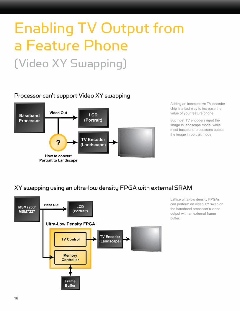
Processor can’t support Video XY swapping
XY swapping using an ultra-low density FPGA with external SRAM
Adding an inexpensive TV encoder chip is a fast way to increase the value of your feature phone.
But most TV encoders input the image in landscape mode, while most baseband processors output the image in portrait mode.
Lattice ultra-low density FPGAs can perform an video XY swap on the baseband processor’s video output with an external frame buffer.
17
720p Wireless Video Streaming from a Smartphone (Image Mirroring and Downscaling)
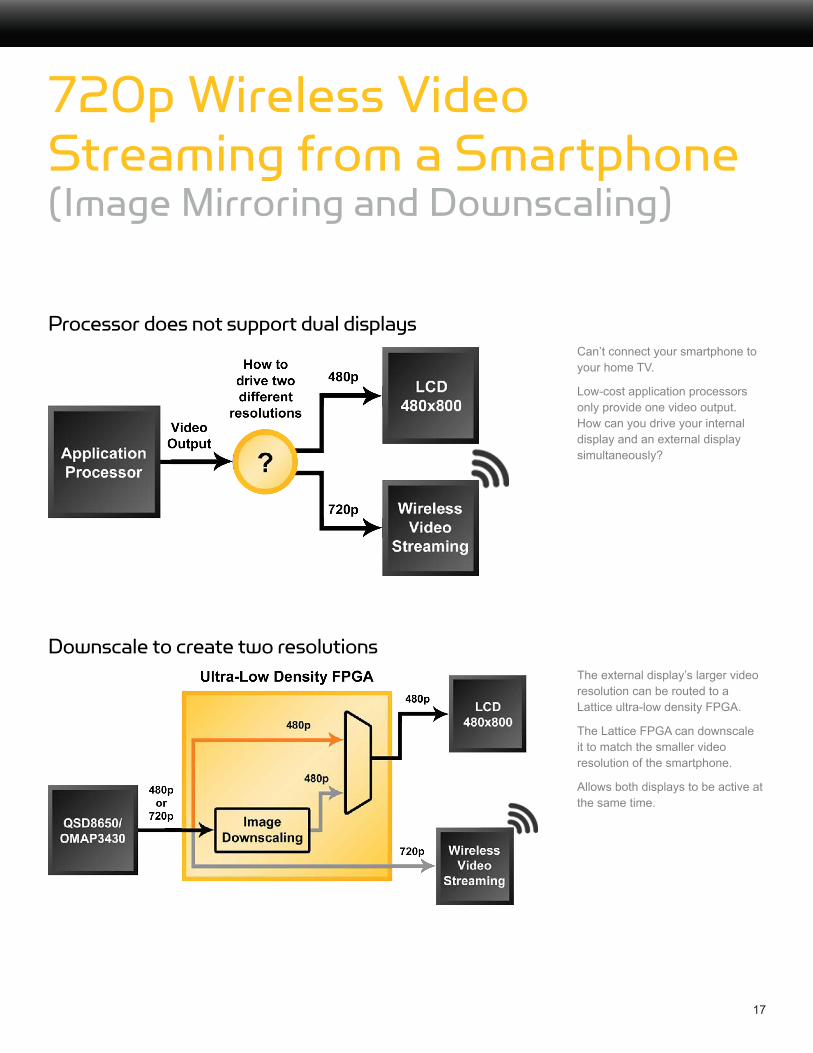
Processor does not support dual displays
Downscale to create two resolutions
Can’t connect your smartphone to your home TV.
Low-cost application processors only provide one video output. How can you drive your internal display and an external display simultaneously?
The external display’s larger video resolution can be routed to a Lattice ultra-low density FPGA.
The Lattice FPGA can downscale it to match the smaller video resolution of the smartphone.
Allows both displays to be active at the same time.

18
3D Video and Imaging(Autostereoscopic 3D Panel Timing Controller)
Processors can’t directly drive autostereoscopic 3D panels
Drive autostereoscopic 3D panel with built-in TCON
3D technology is new and there are no readily available timing controller chips to choose from.
Designers need a flexible timing controller to drive different sized displays.
Lattice ultra-low density FPGAs implement a 3D panel timing controller and drive to a autostereoscopic.
Directly connects to a autostereoscopic 3D display for handset / mobile based products.

19
Universal 3D Shutter Glasses(Customized Pattern Detector for Multiple TVs)
Different TV brands and glasses are often incompatible
Universal shutter glass with pre-defined pattern detection
TV makers define their own IR transmission standard.
This creates incompatibility for different glasses and TVs.
Users have to abandon their glasses when changing to different TV brands.
Lattice ultra-low density FPGAs can implement pattern detection circuits with preloaded patterns to support major TV brands.
In addition, IR noise filtering can be added to offer better quality viewing experience.

20
Managing Differing Video Requirements for Tablets(Color Space Conversion and Timing Controller)Processor can’t convert color space
Use an ultra-low density FPGA for color space conversion and display timing control
Successful tablets must be able to receive video input from multiple sources and display it on multiple devices.
However, this can be challenging for many application processors.
Lattice ultra-low density FPGAs can implement:
• Color Space Conversion• Display Timing Controllers• Image scaling

21
Dual Camera Video for Smartphones and Tablets(Displaying Video-in-Video Images)
Processor lacks multi-camera support
Multi-camera support using an ultra-low density FPGA with external SRAM
Dual cameras are becoming common in smartphones and tablets.
A popular application is to use two cameras to produce a video in video display.
Lattice ultra-low density FPGAs can:
• Convert the camera data to RGB
• Use an external frame buffer to build the video in video image
• Interface the video image to the application processor
22
Enabling Dual Display Cameras(Image Resolution Conversion)
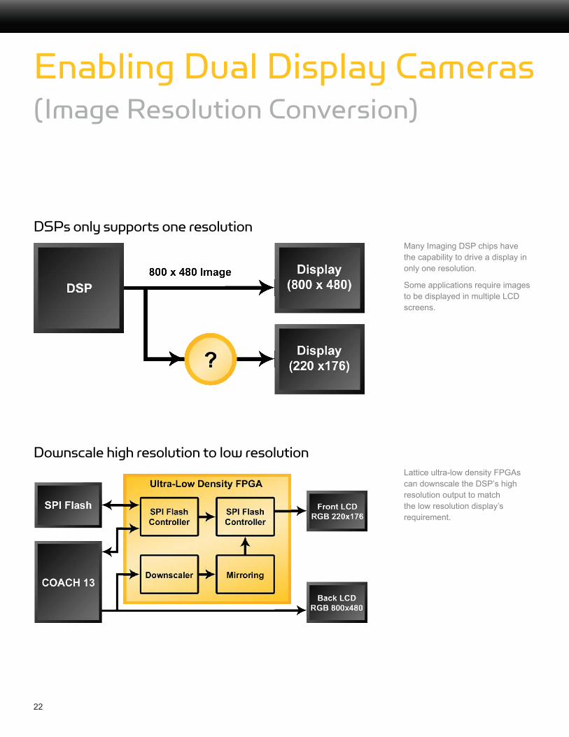
DSPs only supports one resolution
Downscale high resolution to low resolution
Many Imaging DSP chips have the capability to drive a display in only one resolution.
Some applications require images to be displayed in multiple LCD screens.
Lattice ultra-low density FPGAs can downscale the DSP’s high resolution output to match the low resolution display’s requirement.

23
Adopting Managed NAND for Mobile Devices(Built-in eMMC Controller)
Incompatible or lacking eMMC controller
Additional eMMC controller to lower system cost
Some processors have no built-in eMMC controller, unable to take advantage of existing managed NANDs.
Many processors offer eMMC controllers through SDIO ports. However SDIO ports may already be used to connect to other peripherals.
Implement an eMMC host controller inside a Lattice ultra-low density FPGA to take advantage of low cost managed NAND.
An eMMC controller can be customized to a x8 interface for higher performance.

24
Fast Addition of Wi-Fi or CMMB Modules(SDIO to High-Speed Parallel Bus Bridge)Module has two ports, but neither is free
Bridge SD card to AP bus, to free up SD port for Wi-Fi module
A fast way to enhance your product’s feature set is to use readily available modules, such as Wi-Fi or CMMB.
Most of these modules provide SDIO and SPI interfaces.
But what if neither of these interfaces are available?
A Lattice ultra-low density FPGA can implement an SD Host Controller and bridge it to the application processor’s high-speed parallel bus.
This allows the Wi-Fi module to be placed on the SD/SDIO port.
Lattice also provides reference driver code to enable rapid system integration.
25
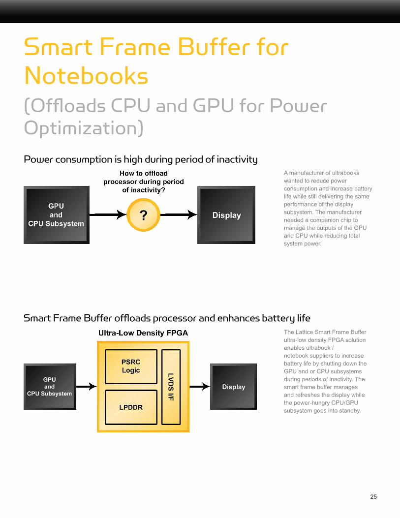
Smart Frame Buffer for Notebooks(Offloads CPU and GPU for Power Optimization)Power consumption is high during period of inactivity
Smart Frame Buffer offloads processor and enhances battery life
A manufacturer of ultrabooks wanted to reduce power consumption and increase battery life while still delivering the same performance of the display subsystem. The manufacturer needed a companion chip to manage the outputs of the GPU and CPU while reducing total system power.
The Lattice Smart Frame Buffer ultra-low density FPGA solution enables ultrabook / notebook suppliers to increase battery life by shutting down the GPU and or CPU subsystems during periods of inactivity. The smart frame buffer manages and refreshes the display while the power-hungry CPU/GPU subsystem goes into standby.
26
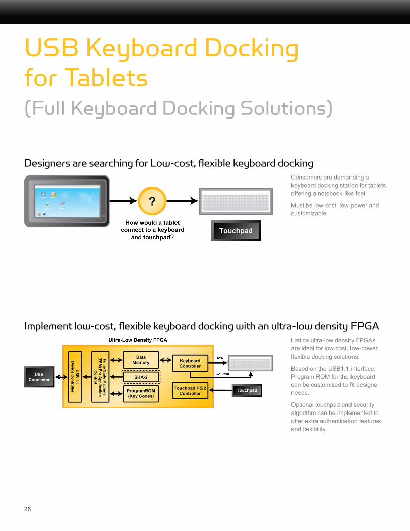
USB Keyboard Docking for Tablets(Full Keyboard Docking Solutions)
Designers are searching for Low-cost, flexible keyboard docking
Implement low-cost, flexible keyboard docking with an ultra-low density FPGA
Consumers are demanding a keyboard docking station for tablets offering a notebook-like feel.
Must be low-cost, low-power and customizable.
Lattice ultra-low density FPGAs are ideal for low-cost, low-power, flexible docking solutions.
Based on the USB1.1 interface, Program ROM for the keyboard can be customized to fit designer needs.
Optional touchpad and security algorithm can be implemented to offer extra authentication features and flexibility.

27
Media Docking for Smartphones(Image Upscaling and Audio Muxing)
Two audio sources must share one speaker and upscaling one
Muxing multiple audio sources and upscale to HDMI
The speaker is shared between built-in radio and smartphone audio output.
Need to output 720p to TV, but the phone only offers 480p.
Lattice’s media docking solution provides an easy way to connect all the audio and video sources from the media devices (radio/smartphone/tablet) to the external world.
The video scaling portion of the design takes video input source from the media device; upscales it and then sends to the external HDMI connector.
In addition, authentication security algorithms, such as SHA-2 can be implemented to guarantee use of vendor-approved parts.
28
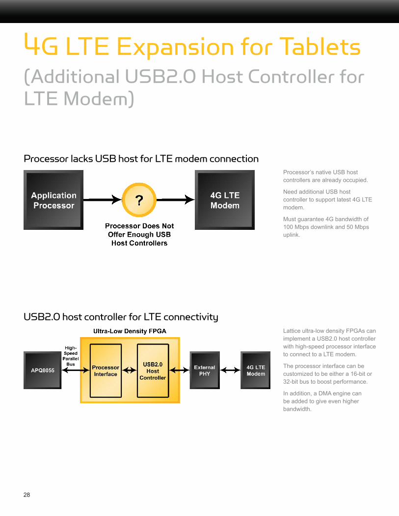
4G LTE Expansion for Tablets(Additional USB2.0 Host Controller for LTE Modem)
Processor lacks USB host for LTE modem connection
USB2.0 host controller for LTE connectivity
Processor’s native USB host controllers are already occupied.
Need additional USB host controller to support latest 4G LTE modem.
Must guarantee 4G bandwidth of 100 Mbps downlink and 50 Mbps uplink.
Lattice ultra-low density FPGAs can implement a USB2.0 host controller with high-speed processor interface to connect to a LTE modem.
The processor interface can be customized to be either a 16-bit or 32-bit bus to boost performance.
In addition, a DMA engine can be added to give even higher bandwidth.

29
Adding High-End Headsets to Smartphones(Nokia ECI Implementation)
Processor does not support high-end audio feature
Implement Nokia’s proprietary ECI for superior audio experience
One role of smartphones is to function as a media player.
Most media players interface to a high end headset, which includes media control functions.
How can this capability be added to a smartphone?
A Lattice ultra-low density FPGA to implement Nokia’s ECI.
Nokia’s Enhanced Control Interface (ECI) is similar to Apple’s Earphones with remote and microphone.
This lets smartphone designers quickly add a high-end audio device interface.

30
Dual SIM Phones(Inter-processor Communication)
How to allow inter-processor communication
Create an Inter-Processor Communication Unit (IPCU)
One way to implement a dual SIM phone is by using two baseband processors.
How can the two processors communicate with each other?
Lattice ultra-low density FPGAs can use any available port on either processor for implementing the inter-processor communication unit (IPCU).
Example interfaces for two processor using a pair of SPI slaves.
31
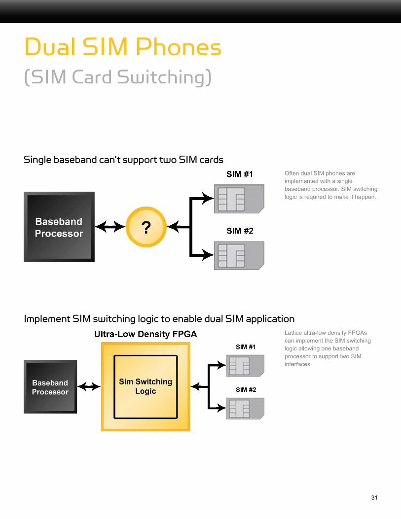
Dual SIM Phones(SIM Card Switching)
Single baseband can’t support two SIM cards
Implement SIM switching logic to enable dual SIM application
Often dual SIM phones are implemented with a single baseband processor. SIM switching logic is required to make it happen.
Lattice ultra-low density FPGAs can implement the SIM switching logic allowing one baseband processor to support two SIM interfaces.
32
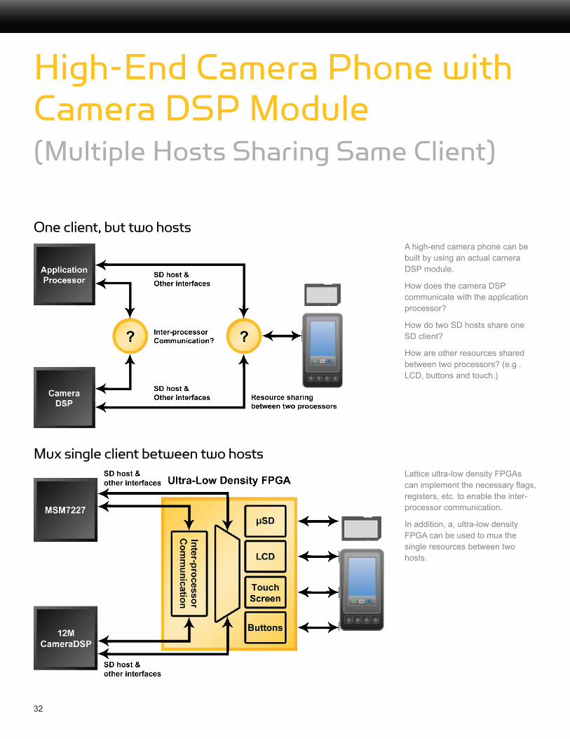
High-End Camera Phone with Camera DSP Module(Multiple Hosts Sharing Same Client)
One client, but two hosts
Mux single client between two hosts
A high-end camera phone can be built by using an actual camera DSP module.
How does the camera DSP communicate with the application processor?
How do two SD hosts share one SD client?
How are other resources shared between two processors? (e.g . LCD, buttons and touch.)
Lattice ultra-low density FPGAs can implement the necessary flags, registers, etc. to enable the inter-processor communication.
In addition, a, ultra-low density FPGA can be used to mux the single resources between two hosts.

33
Adding High-end Features to Low Cost Phones(UART Expansion via the SPI Port)
Processor lacks UART ports
UART port expansion through an ultra-low density FPGA
Adding additional features to a low-cost feature phone can make a big impact on your market share.
But the application processors in low cost phones usually have limited interfacing capacity.
Lattice ultra-low density FPGAs can implement multiple UART controllers and interface them to the application processor’s high-speed SPI port.

34
SLIMbus to I2S
Processor to peripherals interface mismatch
SLIMbus to I2S adapter solves the interface mismatch problem
Processors have implemented SLIMbus to replace traditional audio interfaces like I2S inside the handset. However the audio codecs are slow in adopting the SLIMbus interface, causing an interface mismatch.
Lattice ultra-low density FPGAs can implement a SLIMbus to I2S to solve this interface mismatch problem.
Reversely, an I2S to SLIMbus host controller can be implemented to support the connectivity processor (such as MDM9200) with the SLIMbus interface to hook up to the AP supports only I2S.
35
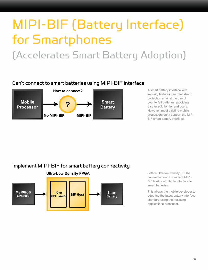
MIPI-BIF (Battery Interface) for Smartphones(Accelerates Smart Battery Adoption)
Can’t connect to smart batteries using MIPI-BIF interface
Implement MIPI-BIF for smart battery connectivity
A smart battery interface with security features can offer strong protection against the use of counterfeit batteries, providing a safer solution for end users. However, most existing mobile processors don’t support the MIPI-BIF smart battery interface.
Lattice ultra-low density FPGAs can implement a complete MIPI-BIF host controller to interface to smart batteries.
This allows the mobile developer to adopting the latest battery interface standard using their existing applications processor.

36
Multiprocessor systems (Custom Interface for Inter-processor Communication)
Sharing critical parameters between two processors
Custom inter-processor communication unit
Dual port RAMs are popular in multiprocessor systems where data needs to be shared between two processors.
However, DPRAMs require high number of I/Os and are not ideal for space constrained applications.
Lattice ultra-low density FPGAs can used to implement I/O optimized custom interfaces to share critical parameters between two processors.
Lattice ultra low density FPGAs are offered in several small packages that meet the requirements of space constrained applications such as Smartphones.

37
SENSOR
MANAGEMEN
T
CONNECTIV
ITY
VIDEO AND
IMAGING
MEMORY
AND STORAGE
CUSTOMMOBILEDEVICE
YOURAP
Mobile ApplicationTargeted IP
CONNECTIVITY
1-to-4 UART Expander
CMOS Camera Interface
PWM (16x3)
I2C Master / Slave Controller
SPI Master / Slave Controller
USB 2.0 Host Controller
USB 2.0 Device Controller
USB 2.0 OTG Controller
USB 2.0 Hub Controller
I2C Master / Slave Controller
PCI Master / Target Controller
MEMORY AND STORAGE
Cellular RAM Controller
MDDR Controller
CF+Controller
MS Pro Interface
NAND Flash Interface
SLC2MLC Interface
MMC Host Controller
SD Host Controller
SDIO Host Controller
MMC Client – MMC Mode Using FPGA RAMs as Memory
SD Client – SD Mode Using NAND Flash as Memory
NOR Flash Controller
Flash Controller with Wear Leveling
LPC Bus Controller
DDR/DDR2/LPDDR Memory Controllers
SDRAM Controller
SENSOR MANAGEMENT
I2C Master Controller
SPI Master Controller
SLIMbus Client Controller
UART
Expansion Memory Interface
Touchscreen Controller
PWM (16x3)
Keypad Scanner
IrDA Fast Tx/Rx
OTHER
Sigma-Delta ADC
Mico8 Microcontroller
LED/OLED Driver
Power Management Bus Controller
CRC (Cyclic Redundancy Checker)
AES Encryption / Decryption
RC4-based pseudo-random sequence generator
MIPI Battery Interface (BIF)
VIDEO AND IMAGING
Dual Display Controller
Graphics LCD Controller
LCD Controller (16x2 Character)
Touch Screen Controller
XGA to WVGA LANCZOS2 Scaler
XGA to WVGA Nearest Neighborhood Scaler
RGB565 to YCbCr 8bit (Color Space Conversion)
RGB666 to YCbCr 8bit (Color Space Conversion)
RGB888 to YCbCr 8bit (Color Space Conversion)
YCbCr 10bit to RGB666 (Color Space Conversion)
YCbCr 10bit to RGB888 (Color Space Conversion)
YCbCr 10bit to RGB565 (Color Space Conversion)
YCbCr 8bit to RGB565 (Color Space Conversion)
YCbCr 8bit to RGB888 (Color Space Conversion)
YCbCr 8bit to RGB666 (Color Space Conversion)
I2C Based Video Switching
Image Blending – Multiple Images and Text Overlay
Image Enhancements – Brightness and Contrast Controller
LVDS Transmitter/Receiver
LVDS Serializer/De-Serializer
DVI Receiver Controller
MIPI DSI Receiver / Transmitter Controller
MIPI CSI-2 Receiver / Transmitter Controller
Dual-LVDS Transmitter (after LVDS Serializer)

38
Lattice Ultra Low Density
FPGA
ReferenceExamples
IPBuildingBlocks
VIDEO ANDIMAGING
MEMORYAND STORAGE
SENSORMANAGEMENT
CUSTOM FUNCTIONS
CONNECTIVITY
STANDARD INTERFACESCUSTOM INTERFACES
STANDARD INTERFACESCUSTOM INTERFACES
3D IMAGING
IMAGE SCALING
ROTATION
VIDEO MUXING
MULTI-DISPLAY
PICTURE-IN-PICTURE
LCD CONTROLLER
COLOR SPACE CONVERSION
ARBITRATION
PRIORITY INTERRUPT
INTERRUPT TRAPPING
POLLING POWEROPTIMIZATION
AGGREGATION
PATTERN RECOGNITION
PROCESSOROFFLOAD
MDDR
SDRAM
DUAL SIM
CF
CELLULAR RAM
NAND FLASH
SD/MMC
SERIAL FLASH
I2C
UART
PWM
SPI
SDIO
GPIO
LVDS USB
Design ServicesIn addition to the Application Examples, Lattice offers a wide range of IP focusing in the areas of Sensor Management, Video and Imaging, Memory and Storage, and Connectivity. Lattice also offers custom design services.
Design Servicesfor CustomChipsets
Off the Shelf,Complete, UniqueDesigns
Broad Selectionfor BuildingCustom Designs

39
Lattice Ultra Low Density
FPGA
ReferenceExamples
IPBuildingBlocks
VIDEO ANDIMAGING
MEMORYAND STORAGE
SENSORMANAGEMENT
CUSTOM FUNCTIONS
CONNECTIVITY
STANDARD INTERFACESCUSTOM INTERFACES
STANDARD INTERFACESCUSTOM INTERFACES
3D IMAGING
IMAGE SCALING
ROTATION
VIDEO MUXING
MULTI-DISPLAY
PICTURE-IN-PICTURE
LCD CONTROLLER
COLOR SPACE CONVERSION
ARBITRATION
PRIORITY INTERRUPT
INTERRUPT TRAPPING
POLLING POWEROPTIMIZATION
AGGREGATION
PATTERN RECOGNITION
PROCESSOROFFLOAD
MDDR
SDRAM
DUAL SIM
CF
CELLULAR RAM
NAND FLASH
SD/MMC
SERIAL FLASH
I2C
UART
PWM
SPI
SDIO
GPIO
LVDS USB
Device Selection Guide
1. MachXO2 (ZE option) measured at 1.2V Vcc2. No PLL available in this package3. Only 1 PLL available4. Ultra high I/O count devices are supported for XO2-HC/HE options5. WLCSP package available for ZE option only6. Contact Lattice sales representative regarding this package, available for HE option only
iCE40 MachXO2
Feature LP384 LP1K LP4K LP8K HX1K HX4K HX8K 256 640/U 1200/U 2000/U 4000 7000
Logic Cells 384 1280 3520 7680 1280 3520 7680 256 640 1280 2112 4320 6864
Embedded RAM Bits 0 64K 80K 128K 64K 80K 128K 0 18K/64K 64K/74K 74K/92K 92K 240K
Phase-Locked Loops 0 1 2 2 1 2 2 0 0/1 1 1/2 2 2
Core Icc @ 0KHz1 21µA 100µA 360µA 360µA 267µA 667µA 1100µA 18µA 28µA 56µA 80µA 124µA 189µA
Memory Standards LPDDR DDR / DDR2 / LPDDR
LVDS Speed 525Mbps 756Mbps
Package Programmable I/O: Max I/O (LVDS Channels)
25-ball WLCSP (2.5 x 2.5 mm)5 18
32-pin QFN (5 x 5 mm) 21 (4) 21
36-ball ucBGA (2.5 x 2.5 mm) 25 (3) 25 (3)2
49-ball ucBGA (3 x 3 mm) 37 (6) 35 (5)64-ball ucBGA (4 x 4 mm) 44
81-ball ucBGA (4 x 4 mm) 55 (3) 63 (8) 63 (9)3
81-ball csBGA (5 x 5 mm) 62 (8)
84-pin QFNS2 (7 x 7 mm) 67 (7)
100-pin TQFP/VQFP (14 x 14 mm) 72 (9)2 55 78 79 79
121-ball ucBGA (5 x 5 mm) 95 (12) 93 (13) 93 (13)
121-ball csBGA (6 x 6 mm) 92 (12)
132-ball csBGA (8 x 8 mm) 95 (11) 95 (12) 95 (12) 55 79 104 104 104
144-pin TQFP (20 x 20 mm) 96 (12) 107 (14) 1074 107 111 114 114
184-ball csBGA (8 x 8 mm)6 150
225-ball ucBGA (7 x 7 mm) 167 (20) 178 (23) 178 (23)
256-ball caBGA (14 x 14 mm) 206 (26) 206 206 206
256-ball ftBGA (17 x 17 mm) 2064 206 206 206
332-ball caBGA (17 x 17 mm) 274 278
484-ball fpBGA (23 x 23 mm) 2784 278 334
40
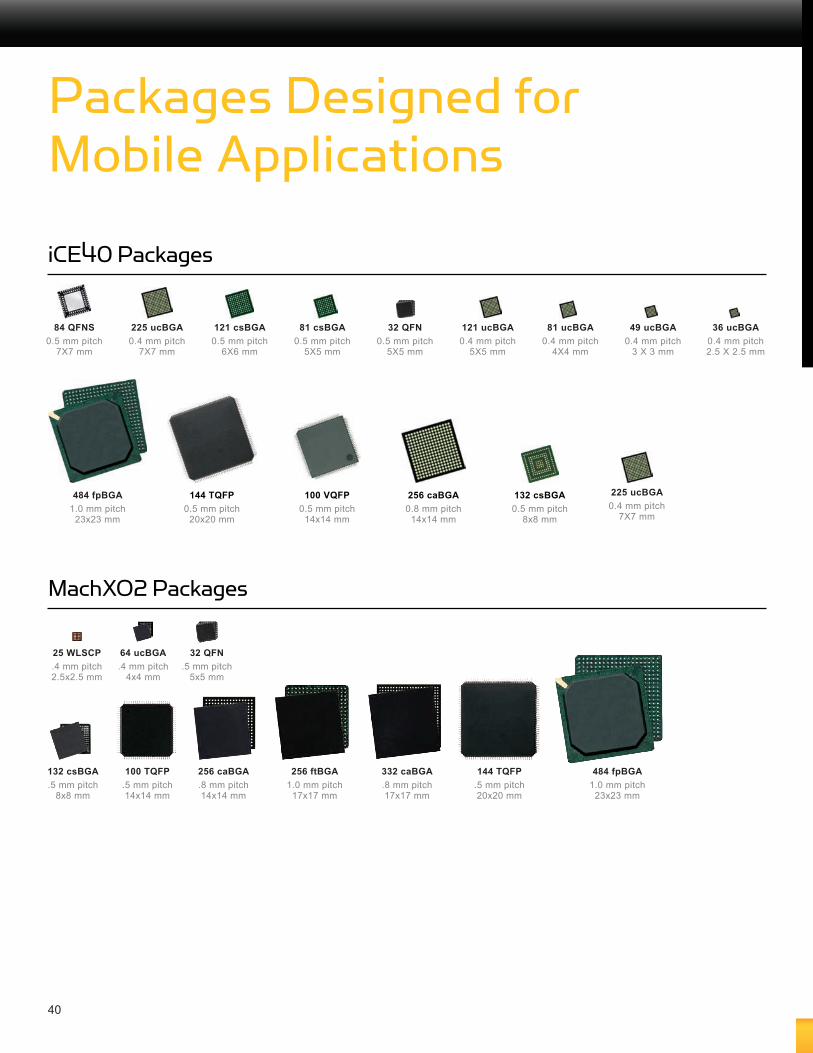
Packages Designed for Mobile Applications
MachXO2 Packages
25 WLSCP.4 mm pitch 2.5x2.5 mm
132 csBGA.5 mm pitch
8x8 mm
100 TQFP.5 mm pitch 14x14 mm
256 caBGA.8 mm pitch 14x14 mm
256 ftBGA1.0 mm pitch
17x17 mm
332 caBGA.8 mm pitch 17x17 mm
144 TQFP.5 mm pitch 20x20 mm
484 fpBGA1.0 mm pitch
23x23 mm
64 ucBGA.4 mm pitch
4x4 mm
32 QFN.5 mm pitch
5x5 mm
iCE40 Packages
84 QFNS0.5 mm pitch
7X7 mm
225 ucBGA0.4 mm pitch
7X7 mm
121 csBGA0.5 mm pitch
6X6 mm
81 csBGA0.5 mm pitch
5X5 mm
32 QFN0.5 mm pitch
5X5 mm
121 ucBGA0.4 mm pitch
5X5 mm
81 ucBGA0.4 mm pitch
4X4 mm
36 ucBGA0.4 mm pitch 2.5 X 2.5 mm
49 ucBGA0.4 mm pitch
3 X 3 mm
484 fpBGA1.0 mm pitch
23x23 mm
225 ucBGA0.4 mm pitch
7X7 mm
144 TQFP0.5 mm pitch
20x20 mm
100 VQFP0.5 mm pitch
14x14 mm
256 caBGA0.8 mm pitch
14x14 mm
132 csBGA0.5 mm pitch
8x8 mm
LATTICESEMI.COM
Copyright © 2013 Lattice Semiconductor Corporation. Lattice Semiconductor, L (stylized) Lattice Semiconductor Corp., and Lattice (design), iCE40, iCEcube2, Lattice Diamond, MachXO2 and ispMACH are either registered trademarks or trademarks of Lattice Semiconductor Corporation in the United States and/or other countries. Other product names used in this publication are for identification purposes only and may be trademarks of their respective companies.
October 2013 Order #: I0222F
Corporate HeadquartersLattice Semiconductor Corporation5555 Northeast Moore CourtHillsboro, Oregon 97124-6421 USATelephone: +1-503-268-8000Facsimile: +1-503-268-8347Web: http://www.latticesemi.com
Software LicensingEmail: [email protected]: http://www.latticesemi.com/licensing/index.cfm
Technical SupportUSA & Canada: 1-800-LATTICE (528-8423)For other locations: +1-503-268-8001PLD Technical and Software: [email protected] Signal: [email protected]
Additionally, customers can receive technical support for Lattice’s Programmable Logic Products from our Asia based applications group, by contacting Lattice Asia applications during the hours of 8:30 a.m. to 5:30 p.m. Beijing Time (CST) +0800 UTC (Chinese and English language only).Asia: [email protected]