i polycrystalline in-film deposition annual techni port ... · national technical information...
TRANSCRIPT
I I ......--------------,
I I NREL/SR-520-23994 � UC Category: 1263
Polycrystalline Cadmium Tell Fabricated by E Annual Techni
in-Film e Solar Cells
deposition port
J.U. Trefny and D. Mao Department of Physics Colorado School of Mines Golden, Colorado
NREL technical monitor: B. von Roedern
National Renewable Energy Laboratory 1617 Cole Boulevard Golden, Colorado 80401-3393 A national laboratory of the U.S. Department of Energy Managed by Midwest Research Institute for the U.S. Department of Energy under Contract No. DE-AC36-83CH10093
Prepared under Subcontract No. XAF-5-14142-11 January 1998

NOTICE
This report was prepared as an account of work sponsored by the National Renewable Energy Laboratory, managed by Midwest Research Institute, in support of its Subcon tract No. XAF-5-14142-11 with Colorado S chool of Mines. Neither the National Renewable Energy Laboratory, nor the Midwest Research Institute, nor Colorado S chool of Mines, nor an y of their emplo yees, nor any of their contractors, nor any of their sub contractors, nor any of their emplo yees, makes an y warranty, express or implied, or assumes an y legal liability or responsibility for the accuracy, completeness or usefulness of an y information, apparatus, produ ct or process dis closed, or represents that its use would not infringe privately owned rights.
This publication was reproduced from the best available camera-ready copy
submitted by the subcontractor and received no editorial review at NREL.
NOTICE
This report was prepared as an account of work sponsored by an agency of the United States government. Neither the United States government nor any agency thereof, nor any of their employees, makes any warranty, express or implied, or assumes any legal liability or responsibility for the accuracy, completeness, or usefulness of any information, apparatus, product, or process disclosed, or represents that its use would not infringe privately owned rights. Reference herein to any specific commercial product, process, or service by trade name, trademark, manufacturer, or otherwise does not necessarily constitute or imply its endorsement, recommendation, or favoring by the United States government or any agency thereof. The views
and opinions of authors expressed herein do not necessarily state or reflect those of the United States government or any agency thereof.
#.
Available to DOE and DOE contractors from: Office of Scientific and Technical Information (OSTI} P.O. Box62
Oak Ridge, TN 37831 Prices available by calling (423) 576-8401
Available to the public from: National Technical Information Service ( NTIS) U.S. D epartment of Commerce
5285 Port Royal Road Springfield, VA 22161 (703) 487-4650
'• J Printed on paper containing at least 50% wastepaper. including 20% postconsumer waste

Executive Summary
Objectives
The objective of this project is to develop improved processes for the fabrication of CdTe/CdS polycrystalline thin film solar cells. The technique we use for the formation of CdTe, electrodeposition, is a non-vacuum, low-cost technique that is attractive for economic, large-scale production.
Technical Approach
During the past year, our research and development efforts have focused on several steps that are critical to the fabrication of high-efficiency CdTe solar cells. These include the study of growth and properties of electrodeposition CdS, quantitative studies of CdTe-CdS interdiffusion using x-ray diffraction and photoluminescence, and back contact formation using Cu-doped ZnTe with an emphasis on low Cu concentrations. We have also started to explore the stability of our ZnTe-Cu contacted CdTe solar cells.
Results
Studies of the �rowth and properties of electrodeposjted CdS thin films. Uniform, high-quality CdS thin films are highly desirable for the fabrication of high
efficiency CdTe/CdS solar cells. Currently, chemical bath deposition is the most successful among all techniques. Other techniques, such as vacuum sublimation, have been used. However, because of a higher density of pinholes in the deposited films, the minimum CdS thickness required for obtaining high V oc is much greater than for CBD CdS. Electrodeposition is a non-vacuum technique and is compc:ttible with our CdTe deposition process. Moreover, it offers excellent control over the properties o(the thin films through the influence of deposition potential, bath temperature, pH, andcomposition of reactants. We have investigated the electrodeposition of CdS and its application in fabricating CdTe/CdS solar cells. The electrodeposition of CdS was done in a system that consisted of a glassy-carbon anode, a Ag/AgCl reference electrode, and a cathode (sample substrate). The experimental conditions we explored in this study were: pH from 2.0 to 3.0; temperatures of 80° and 9 Q<C; CdCl2 concentration of 0.2 M; deposition potential from -550 to -600 mV vs. Ag/AgCl electrode; [Na2&Q] concentration between 0.005 and 0.05 M.
The electrodeposition rate of CdS was studied as a function of the solution temperature, sodium thiosulfate concentration, pH, and the acid used. The deposition rate increases with increase of the thiosulfate concentration and decrease of solution pH. Such a dependence can be understood based on the known disproportion of thiosulfate ions. With decreasing pH and increasing thiosulfate concentration, the disproportion rate increases, leading to increased deposition rate of CdS on the electrode. The high deposition rate observed at high solution temperature may be caused by both an increased reaction rate at the electrode and the increased thiosulfate disproportion rate. We also observed that the acid used to adjust the pH has a large impact on the deposition rate. The deposition is faster in a hydrochloric acid solution than in a sulfuric acid solution. The Faradaic efficiency of the electrodeposition process was calculated. The Faradaic efficiency is lower at low pH, caused presumably by the hydrogen evolution at low pH which contributes to the reduction current. In all
lll
cases, the Faradaic efficiency was much lower than unity. The surface morphology of electrodeposited CdS thin ftlms was investigated using scanning
electron microscopy. The most pronounced difference in ftlm morphology was observed for different solution temperatures. Films d,eposited in a hydrochloric acid solution at 80<C consist of agglomerates of small crystallites. These agglomerates have a rather uniform size of -0.7 J.Lm and cover the tin oxide substrates uniformly. Films deposited at a higher temperature of 90oC are nonuniform with J.Lm-size CdS agglomerates covering only a small portion of the substrates. Therefore, in terms of ftlm uniformity and cell fabrication, deposition in a hydrochloric acid solution at 80<C is preferred. The improved uniformity can be related to the slow growth rate obtained under such conditions. The composition of the electrodeposited CdS was analyzed using Auger electron spectroscopy. The ratio of Cd and S concentrations is close to the stoichiometric value for films deposited at pH of 3.0. At lower pH, the films are more Cd rich. We have prepared CdTe/CdS cells using electrodeposited and physical vapor deposited CdTe on electrodeposited CdS. Moderate cell efficiencies were obtained in the preliminary study.
Studies of Cu-doped ZnTe back contact layer The formation of stable, low-resistance back contacts to polycrystalline CdTe is a critical
step in development of high efficiency CdTe thin ftlm solar cells. One back contact material, Cudoped ZnTe, has yielded very low contact resistance (<0.1 ohm.cm2) and high fill factors (>0.74) in CdTe solar cells [1, 2]. Because of the high diffusivity of Cu in polycrystalline thin films, it is desirable to bring the Cu doping concentration to as low a level as possible while still maintaining the performance of the contact. We have extended our previous research on ZnTe:Cu films by investigating films doped with low Cu concentrations ( <5.0 at. % ). The low Cu concentration enabled us to increase the ZnTe:Cu post-deposition annealing temperature without causing excessive Cu diffusion into CdTe or formation of secondary phases. The effects of low Cu doping level and high temperature annealing on the stability of the CdS/CdTe/ZnTe devices were also investigated.
The effects of Cu doping concentration and post-deposition annealing temperature on the structural, compositional, and electrical properties of ZnTe were studied systematically using xray diffraction (XRD), atomic force microscopy (AFM), electron microprobe, Hall effect and conductivity measurements. XRD measurements indicated that the crystalline phase of as-deposited and low-temperature annealed ZnTe films is dependent on Cu doping concentration. Low-Cudoped ftlms exhibited zincblend phase, whereas high-Cu-doped films showed wurzite phase. After annealing at high temperature (� 350C), all films exhibited zincblende structure. Electron probe microanalysis revealed a deficiency of cations in low-Cu-doped films and excess of cations in highCu-doped films. Hall effect measurements revealed a dependence of hole mobility on Cu doping concentration with the highest mobility (20 cm2Ns) obtained at a low Cu concentration. Carrier concentrations higher than mid-101SCm-3 were obtained at a Cu concentration of 2 at. % and relatively low annealing temperatures. Studies of the activation energy of dark conductivity suggested that intrinsic defects (e.g., Zn vacancies) are dominant acceptors for Cu concentrations lower than 4.5 at. % . Finally, ZnTe films with Cu concentrations as low as 1 at. %were used successfully as a back contact layer in CdTe based solar cells. Fill factors over 0.70 were obtained using ZnTe films of low Cu doping.
iv
r i
r I
[ Table of Contents
iii
v
I vi
vii
r 1 .
Executive Summary
Table of Contents
List of Figures
List of Tables
Introduction 1
1 . 1 Background 1
1 .2 Cell Fabrication Procedure 1
2. Electrodeposited CdS Films and
Their Application in CdS/CdTe Solar Cells 2
Electrodeposition Process 2
Structural and Compositional Analysis 5
Solar Cell Fabrication Using Electrodeposited CdS 8
3. Effect of Cu Doping on the Properties
of ZnTe:Cu Thin Films and the CdS/CdTe/ZnTe Solar Cells 10
Compositional Analysis 10
Hall effect and Conductivity Measurements 12
Optimization of ZnTe Contact Formation
on GPI and SCI CdTe/CdS Films 15
Mechanism and Stability Studies 18
4. Fabrication of CdTe/CdS Cells on Ti(h 20
5. Other Team Activities 21
6. Summary 22
7. Acknowledgements 2 3
8 . References 2 3
9. Appendices 24
9. 1 Personnel 24
9.2 Laboratory Improvements 25
9. 3 Publications 25
v

List of Figures
Figure 1. The deposition time required for the passage of 0.16 Coullcm2 charge as a function of the sodium thiosulfate concentration and solution temperature.
Figure 2. The deposition time required for the passage of 0.16 Coullcm2 charge as a function of the sodium thiosulfate concentration and solution pH.
Figure 3. The deposition time required for the passage of 0.16 Coul/cm2 charge as a function ofsolution pH and the acids used.
Figure 4. The Faradaic efficiency of the electrodeposition process as a function of solution pHand the acids used.
Figure 5. SEM images of electrodeposited CdS.
Figure 6. SEM images of CdS films electrodeposited on (a) Sn02 and (b) ITO substrates.
Figure 7. X-ray diffraction of electrodeposited CdS. The peaks are identified as: 1: (lOO)h; 3: (101)h; 4: (200)c; 7 : (llO)h or (220)c. Peaks 2, 5, 6 are dominated by Sn02.
Figure 8. Atomic concentration of Zn, Te, and Zn+Cu as a function of Cu doping concentration in the ZnTe films.
Figure 9 . X -ray photoemission spectra of Te 3d and Cu 2p core levels of ZnTe:Cu films.
Figure 10. Temperature dependence of dark conductivity of a ZnTe film doped with 2 a t . %
of Cu. Figure 11. Light 1-V curves of CdTe/CdS cells fabricated on Ti02-coated Sn02
substrates.
vi

List of Tables
Table 1 . Composition of CdS films prepared with electrode position.
Table 2. Cells made with the standard annealing conditions (annealing of CdTe/ CdS films, coated with CdCl2, in air at 4100C for 45 min).
Table 3. Cells made with the modified annealing conditions. Sample #5 was not annealed prior to the deposition of the CdTe films. The cells of ED#7 and E D#8 are contacted with ZnTe/ Au.
Table 4 . Cells made with physical vapor de posited CdTe on electrodeposited CdS.
Table 5. Composition of ZnTe doped with different amounts of Cu (measurement performed by Alice Mason of NREL). The film thickness was 0.8 Jlm.
Table 6. The dependence of film resistivi ty, sheet resistance, carrier concentration and mobility of ZnTe as a function of Cu concentration and post-de position annealing temperature. The film thic kness was 0.8 Jlm.
Table 7. Activation energy of dark c onductivity of Zn Te films as a function of Cu concentration and post-deposition annealing temperature.
Table 8. Performance of cells with different Zn Te:Cu annealing temperature. The Cu concentration was 2.0 at. %. The thickness of ZnTe was 80 nm.
Table 9 . Performances of cells fabricated with different Zn Te :Cu thic knesses. The Cu concentration was 4 .0 at. %. The annealing temperature was 250 0C .
Table 10 . Performance of cells fabricated with ZnTe contacts on GPI films.
Table 1 1 . Optimization of Cu concentration in ZnTe for SCI CdTe/CdS films.
Table 12 . Cell performance as a function of ZnTe post-deposition annealing temperature. The Cu concentration was 2 .0 at. %, ZnTe film thickness was 50 nm.
Table 13. Effect of Cu concentration in ZnTe on doping density and depletion width of CdTe deduced from capacitance-voltage measurements of cells .
Table 14. CdTe doping density as a function of annealing temperature. The Cu concentration was 2 .5 at. %.
Table 1 5 . Cell performance after temperature stress (1 500C) in the dark. The cells were at o pen circuit with no external applied bias.
Vll

Table 16. The CdS thic kness and treatment conditions .
Table 17. The photovoltaic performance of the cells listed in Table 16.
Vlll
I l
l

1. Introduction
1.1 Background
Polycrystalline thin-film CdTe has attracted a great deal of interest for low-cost, high efficiency photovoltaic energy conversion applications. Among the various techniques that are availa ble for CdTe thin film deposition, electrodeposition is a non-vacuum technique and has the advantage of low cost , efficient utilization of raw material, and scalability for high-volume production. The objective of the CSM contract was to improve certain processing steps of the cell fabrication and to further our knowledge of the polycrystalline thin film materials. Improvedefficiencies, high-quality film growth techniques, materials analysis, device fabrication and characterization have all been of particular interest in our work.
1.2 Cell Fabrication Procedure
The solar cell s tructure we investigate has a CdTe/CdS/SnOiglass structure. The standard cell fabrication procedure includes :
(1) Preparation ofCdS thin films (typical thickness of0.2 Jlm) by chemical bath deposition (CBD) or electrodeposition. CBD was performed in an alkaline solution containing cadmium acetate, ammonium acetate, ammonium hydroxide, and thiourea. Electrodeposition was done in an acidic solution containing CdCh and Na2S203.
(2) Annealing of the CdS films at 45 o·c for 50 min in a N2 atmosphere. A CdClz coating was applied to the CdS surface prior to annealing, using a mist generator containing a 1 . 2 M CdCb aqueous solution.
(3) The electrodeposition of CdTe (typical thickness of 2 - 3 .5 Jlm) using a system comprised of four electrodes : Cd and Te anodes, a Ag/ AgCl reference electrode, and a cathode (sample substrate). The typical electroplating conditions were : pH, 2; temperature, 8 o·c; 1 .2 M CdCl2; deposition current between 0.26 and 0.40 mA/cm2; deposition potential, -600 mV (vs.Ag!AgCl electrode); and anode current ratio close to 2.0.
( 4) Annealing of CdTe/CdS films at 41 o·c for 40 min in dry air. Prior to annealing, a CdCl2coating was applied to the CdTe surfaces using the same procedure as used for the CdS layers.
(5) Etching of the CdTe surface in a 0.1% Br-MeOH solution for 10 s. (6) Deposition ofZnTe films doped with Cu by vacuum evaporation. Cu concentration was
varied between 1 and 8 at. %. The ZnTe :Cu layer thickness was varied from 40 to 150 nm. (7) Post-deposition annealing in a Nz environment in the temperature range of 170 to 280 ·c. (8) Metal evaporation.
A wide variety of thin film and device characterization techniques were used to characterize our material. X-ray diffraction (XRD) measurements were performed on a Rigaku x-ray diffractometer using Cu-Ka radiation. Scanning electron microscopy (SEM) measurements were performed using a JOEL Model 840 instrument. Optical transmission and reflection measurements were performed using a CARY 5E UV-VIS-NIR spectrophotometer equipped with a PTFE integrating sphere. The finished cells were characterized using current-voltage, capacitancevoltage, and spectral response techniques.
1
2. Electrodeposited CdS Thin Films and Their Application in CdS/CdTe Solar Cells
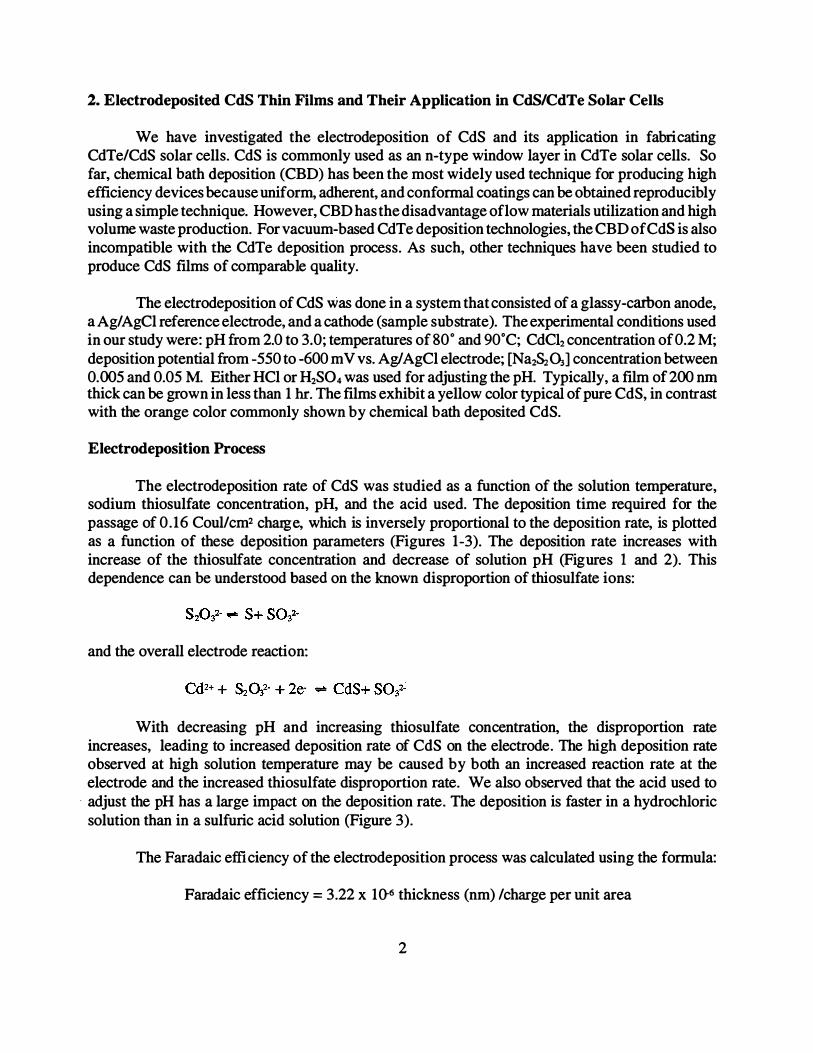
We have investigated the electrodeposition of CdS and its application in fabricating CdTe/CdS solar cells. CdS is commonly used as an n-type window layer in CdTe solar cells. So far, chemical bath deposition (CBD) has been the most widely used technique for producing high efficiency devices because uniform, adherent, and conformal coatings can be obtained reproduciblyusing a s imple technique. However, CBD has the disadvantage oflow materials utilization and high volume waste production. For vacuum- based CdTe deposition technologies, the CBD ofCdS is also incompati ble with the CdTe deposition process. As such, other techniques have been studied to produce CdS films of comparable quality.
The electrodeposition of CdS was done in a system that consisted of a glassy-carbon anode, a Ag/ AgCl reference electrode, and a cathode (sample substrate). The experimental conditions used in our study were: pH from 2.0 to 3.0; temperatures of 80° and 90oC; CdCh concentration of 0. 2 M; deposition potential from -550 to -6 00 m V vs. Ag/ AgCl electrode; [Na2��] concentration between0. 005 and 0.05 M. Either HCl or H2S04 was used for adjusting the pH. Typically, a film of2 00 nmthick can be grown in less than 1 hr. The films exhibit a yellow color typical of pure CdS, in con trast with the orange color commonly shown by chemical bath deposited CdS.
Electrodeposition Process
The electrodeposition rate of CdS was studied as a function of the solution temperature, sodium thiosulfate concen tration, pH, and the acid used. The deposition time required for the passage of 0.16 Coul/cm2 charge, which is inversely proportional to the deposition rate, is plotted as a function of these deposition parameters (Figures 1-3). The deposition rate increases with increase of the thiosulfate concentration and decrease of solution pH (Figures 1 and 2). Thisdependence can be understood based on the known disproportion of thiosulfate ions:
and the overall electrode reaction:
With decreasing pH and increasing thiosulfate concentration, the disproportion rate increases, leading to increased deposition rate of CdS on the electrode. The hi gh deposition rate o bserved at high solution temperature may be caused by both an increased reaction rate at the electrode and t he increased thiosulfate disproportion rate. We also observed that the acid used to
· adjust the pH has a large impact on the deposition rate. The deposition is faster in a hydrochloric solution than in a sulfuric ac id solution (Figure 3).
The Faradaic efficiency of the electrodeposition process was calculated using the formula:
Faradaic efficiency = 3. 2 2 x 1 Q-6 thickness (nm) /charge per unit area
2 f l

• •90°C 100 f-.
• 80°C
-c •
E 80-Q) E
F • c g en
60 0 0. Q)
0 •
40 -
•
r r I • 0.01 0.02 0.03 0.04 0.05
[Na2S203] (M)
Figure 1. The deposition time required for the passage of 0.16 Coul!cml charge as a function of thesodium thiosulfate concentration and solution temperature. The solution pH was 3.0. The acid used was HCI.
45 �
-c E 40 � -CD E ..... 35 -c � a; • 0 g- 30 r-0
25 f-.
I
0.01
• •
0.02
•
I
0.03
[Na2S203] (M)
-•-pH:2.5 -•-pH:3
• '
0.04 0.05
Figure 2. The deposition time required for the passage of 0.16 Coullcm1 charge as a function of the
sodium thiosulfate concentration and solution pH. The solution temperature was 900C. The acid used
was HCl.
3

.A.HCI •
+ H2S04 40 1-
- • c
§. 35 t-CD E i= c 30 t-2
<n 0 0. CD 25 t-0
•
20 t-A I I I
2.4 2.6 2.8 3 3.2 3.4
pH Figure 3. The deposition time required for the passage of 0.16 CouUcm% charge as a function ofsolution pH and the·acids used. The solution temperature was 9o·c.
� c CD 0 ::: CD 0
0.4 t-
as 0.3 r-e "0 eca
u..
0.2 t-
•
2.3
I I
2.4 2.5
•
•
•
•
I I
2.6 2.7 2.8 2.9 3
pH
Figure 4. The Faradaic efficiency of the electrodeposition process as a function of solution pH andacids used. The solution temperature was 9o·c.
4
I l
f {
{

The results are shown in Fig. 4 for deposition in both hydrochloric and sulfuric acid solutions. The Faradaic efficiency is lower at low pH. This is caused presumably by the hydrogen evolution at low pH which contributes to the reduction current. In both cases, the Faradaic efficiency was much lower than unity.
Structural and Compositional Analysis
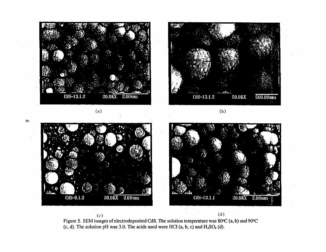
The morphology of electrodeposited CdS was studied using SEM. The most pronounced difference in film morphology was observed when the temperature of the solution was changed. Fig. 5 shows the SEM images of CdS films electrodeposited under different conditions. Films deposited in a hydrochloric acid solution at 80<C (Fig. 5 a, b) consist of agglomerates of smallcrystallites. These agglomerates have a rather uniform size of -0.7 J.lm and cover the tin oxide substrates uniformly . The crystallites that compose these agglomerates have a typical size of 50 nm. Films deposited at a higher temperature 90<C (Fig. 5 c) are nonuniform with J.lm-size CdS
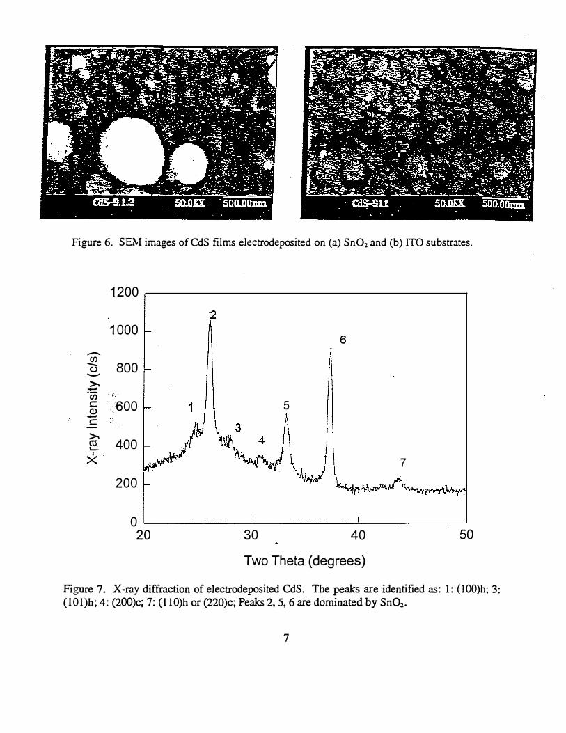
agglomerates covering only a small portion of the substrates. Films deposited in a sulfuric acid solution at 90oC (Fig. 5 d) are also nonuniform, consisting of agglomerates of varying sizes that cover the substrates completely. Therefore, in terms of film uniformity and cell fabrication, deposition in a hydrochloric acid solution at 80oC is preferred. The improved uniformity can be related to the slow growth rate obtained under such conditions. We have also investigated the effects of substrate materials. Fig. 6 shows the SEM images of films deposited on tin oxide and indium-tin-oxide (ITO) substrates. Films deposited on ITO substrates are much more uniform than films deposited on tin oxide substrates under the same deposition conditions (pH 3 .0 and 90<C).
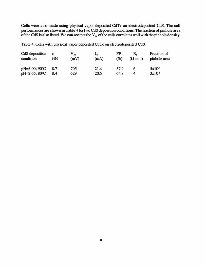
X-ray diffraction was used to characterize the crystalline phase of the electrodeposited CdS. Fig. 7 shows the typical result. The assignment of the peaks is given in the Figure caption. In addition to peaks that may correspond to either cubic or hexagonal CdS (peak 7), we observed several peaks that are present either in hexagonal phase only (peak 1 , 3) or in cubic phase only (peak 4) , indicating that the electrodeposited CdS is a mixture of hexagonal and cubic phases. This isdifferent from the chemical bath deposited film which, according to our previous study, exhibited only cubic phase.
The composition of the electrodeposited CdS was analyzed using Auger electron spectroscopy. The results are listed in Table 1 .
Table 1 . Composition of CdS films prepared with electrodeposition.
Samples
ED (pH =3) ED (pH = 2.65)
Cd (at. %)
40.6 44.4
S (at. %)
36.2 29 .7
O(at. %)
3.7 5.5
C (at. %)
13.7 1 1 .5
O( a %)
5 .5 8.4
The ratio of Cd and S concentrations is close to the stoichiometric value for films deposited at a pH of 3.0. At lower pH, the films are more Cd rich.
5
0\
--� .,... . .. .... ..... s•- , .. ,,... '''j;'•'' of·� ·-t::· . •. ·-· "•:1 JJi'�i;li'j . ... I ;i:� p.� . --·>.W·'�I· ·, .. \if'J"'II" •. '\ ... ���·�f. I
•. � .. .. ��: ·-. . .. . ·.
. . �,: ': ·: �··. . -·; .. ·: :: i';;J!I/ . : ���··:.. . • -� .! �:��- j J��}l/i. . /r��-: · ·:··· ·-'· · ··· · .. · ' ·,; · � .-� 1 '.ft1.}.'��.�1t' <.��·i;_·.�Jl, . . ;, :::l;< . ··:..:,:-�� ·.,. ' .• :;��-,·: ·. ·
·: . -� <;$;:_�151· '�_:':?_�� .. ·: · '· ;: -:j� ) . '
.
.?�.��) . . :1
· . . ; .. _..,_) . . .. ··'J' ·'* ··w .
.
.
.
.
_;•r.
.
··� ·��·-·a-�·��.�:- · -1�:?; �·�··�: -�.:\'· , . .�:·+ ··: ·��_:·�:; �� ·�· . . . ; .p. ..· ·�·· .. �� .,,,. ��.: . . :.:. ' >� ::. :, ... , �;:?��r: - ; ;:. �:· . .
.;.t, . .. ! i. �· .
. !·�:· t1�"1· . J)? · • ··; •·.- , · I ,,.
�:'1:.· .. , . ..,. ·"'· • ' .. . =�! (•!"t):' . • � ,.·. .�·. ··�·..
. • •.
· ·. :.. . 'I • " ' *"'" ./f}> 48 .. ' . · ·�nr·..
•. ·.:::. ··-•. , ' . -.� '·.�:�'J . ;;�.:ttl{{!�;.� .;. .J\; ,•; . . ';., '.�·:. ·.
. :·:· � - . ... . .. /'·� i '��'.;'WJ; ;,'r :.·.;\: . :; :.. ·.�.1·· ·.<'.·. ��JL.t.�f :·. '·:¢''\. : .. ' r . . :•
·· ; "' rt. ·. . :;:-_•{ '· ·;;·. ·.·::I. . :�.!.� :·•)(' ' �. . : ::••rf.ol· · 1 ��{.••
• : •. ...· ; .. l};o·,_ . . � .. (,.,, . : , .. t .. '.':� ... ...... · . .. !6 ,. · . I . ' . . . . ,. .• ,;;:<..:;�;It�..- . •ru!SriU.. -\.1
CdS-13.1.2 20.01\X 2.0Uum
(a)
. !:,-·.,.:· .. ··· t ._,,.;: .. · . �; -:;: • ··,, . • '
tl Ul.;'· '._
. .
($t .� '. A •
. 1·�L:�. t;A : ·r •' ·.' ; � .. : '
;· t I •• ' ., . . . . ""� • � ...
. . ' l.i""! ;·�r�;�. f� �-J_·. •·•. · t�.
·
.
-···.: \
.� ·r,�-·
1: �' . . '.'l?. / ... !, :-\:'].: ' :. � . . ,., I . . ... . � . . � .... "" � . .
-· · · · ·· · ·� ' �· � · <t:" �� . t . c. • tt.,� ... •' . . . t . . ·. � .
' • '
� -. • • . I • • 1 - 1;
�, - ' �.
• (' I �
,,
•
.
'r.
·:.
,.... • �< � � .
.
. � . ·.� ·
.
:� . . . ,) ;;;;jlp� 1· · ·•· . t. . . .. /� : . �,,� ·.3J! ..
.t�· •. ; . . ('
..
;:t��-
: ; · ·� . ,. . . �. -�
·�· · . . .... ·� .... ��· . . . ''·' . ...... '
' ,..,� . '•,: ··=-�;.J: .. ' . �� . f yl; -� � y • �,t IJ
-..
·8,
�
.'
., ...... ., • I . . . . .· � .•.. ·.�. :. ;.. . . . •: .. (1 . .
" 1:'. �ail .. '' .. d. . . . � � -<;,,IJ · ..
- 1� .. : .,.:, .. h
t'dS-9.1.2
. .· ... , . .
. ,,J
j
•
·
:�.
· .-� . .. .,,·..,. .. •
. i•"'A -.
•
• I
;i�-
(b)
' ·� • ··���� -� ""'!': r� . . .t�'lf� Q.1 ' i,..- · ·.·� ';:.�.;t :�>. �r. �,.., ... -�. :.mJ .�· ·� '--� ... \, ,·; , . ,, · :·, "ttf - · ; . . · . � . "' .. · '· . .. ,� . ·�·-4 ,,,. t . ' \I; .... :\. . .. .
.•.,
"'
. , :' . :r�o�i � . . ·�;:-�-/� . .; 'iM•r' .• . .i.• • •· • . • . ,":''tf.v ·.· ��� ·� · :� ��--tl "·'' . .. J} ':.;,� ··:
1, ' • t . >>) ·.. ·.:- . '·.}·.��" ·:'
. 1,. 1 . \'��... . .:�.. . . i:i't ��� �;. :j ··�· .. :;.\. . . - : ··':1''' "�� �. .• <:'·!1:··:. :' :.. :" -!::>: • '
. '·i�� ��· :��· � ·.\ .. i i ···"' :-. :··� . : .•• . \, !'•f ·. f_!] .,� :. : · l· - ·'f '� St
. '·• � .,.��l·· ·'·�.. .kl-� � :':1 � :-���, :·� :,. :·N�·�. · :·�
··"·· :A�' <�?F.�·� � ; ,, • ..r:.:� ;M� _�_..� :) -··.�,:ot�
CdS-13.1.1 20.0KX 2.00Wll .f ·. f• • \1'
(c) (d) Figure 5. SEM images ofclectrodeposited CdS. The solution temperature was 800C (a, b) and 9 00C (c, d). The solution pH was 3.0. The acids used were HCI (a, b, c) and H2S04 (d).
�
� �
Figure 6. SEM images ofCdS films electrodeposited on (a) Sn02 and (b) ITO substrates.
1200
1000 6
-CIJ - BOO (.) ->-
:!::::::: CIJ c :600 Q) -c
>-400 CO. L..-
I X
200
5
��J\¥j 7
0 �----------�------------�----------� 20 30 40 50
Two Theta (degrees)
Figure 7. X-ray diffraction of electrodeposited CdS. The peaks are identified as: 1 : (IOO)h; 3: (IOl)h; 4 : (200)c; 7: (llO)h or (220)c; Peaks 2, 5, 6 are dominated by Sn02•
7

Solar Cell Fabrication Using Electrodeposited CdS
We have prepared CdTe/CdS cells using electrodeposited CdS films. We found that in comparison to the CdS films grown by chemical bath deposition, electrodeposited CdS fi lms have poor adhesion to the tin oxide substrates and flake off easily during CdTe deposition or postdeposition annealing. This problem is especially severe when the CdTe films are thick or when the CdS fi lms are not annealed prior to CdTe deposition. When our standard CdTe/CdS annealing procedure was used, cells made with electrodeposited CdS exhibited a low open-circuit voltage and a low shunt resistance, resulting in low efficiency of the cells (Table 2).
Table 2. Cells made with the standard annealing conditions (annealing of CdTe/CdS films, coated with CdC12, in air at 41 OOC for 45 min).
Sample 11 Voc JS<: FF Rs Rsh (CdS thickness) (%) (mV) (rnA) (%) (Q-cm2)
#4 (50 nm) 4.68 371 23.8 52.9 6 .54 194 #6 (125 nm) 2.86 298 22.8 42.0 6.93 54.2 #8 (250 nm) 4.67 383 21 .7 56.1 5.43 1 85
We have modified the post-deposition annealing procedure in order to improve the adhesion of CdTe/CdS films formed on electrodeposited CdS. Significant improvement was o btained in terms of V oc, Rsh, and the resulting cell efficiency. The open-circuit voltage of 0.65 V and efficiency of 7 .7 % obtained with a CdS film thickness of 125 nm are comparable with what we obtained with CBD CdS of a comparable thickness. However, at larger CdS thicknesses, the efficiency of cells fabricated with electrodeposited CdS is much lower than what we obtain typically (upper 700 m V range) with CBD CdS.
Table 3. Cells made with the modified annealing conditions. Sample #5 was not annealed prior to the deposition of the CdTe films. The cells of ED#7 and ED#8 are contacted with ZnTe/Au.
Sample 11 Voc JS<: FF Rs Rsh (CdS thickness) (%) (mV) (rnA) (%) (Q-cm2)
#4 (50 nm ) 5.73 433 24.5 53.8 6.94 1 89 #5 (125 nm) 7.68 654 24.4 48.0 1 1 .3 126 #6 ( 125 nm) 6.63 503 23 .2 56.6 8 .28 382 #7 (185 nm) 7.08 61 2 20.1 57.4 5.55 167 #8 (250 nm) 7.30 5 18 22.6 62.1 4.74 376
8
t ..
Cells were also made using physical vapor deposited CdTe on electrodeposited CdS. The cell performances are shown in Table 4 for two CdS deposition conditions. The fraction of pinhole area of the CdS is also listed. We can see that the V oc of the cells correlates well with the pinhole density.
Table 4. Cells with physical vapor deposited CdTe on electrodeposited CdS.
CdS deposition , Voc Jsc FF Rs Fraction of condition (%) (mV) (rnA) (%) (Q-cm2) pinhole area
pH=3 .00; 900C 8 .7 705 21 .4 57.9 6 5x1 Q-6 pH=2.65; 800C 8.4 6 29 20.6 64.8 4 3xl Q-5
9
3. Effect of Cu Doping on the Properties of ZnTe:Cu Thin Films and the CdS/CdTe/ZnTeSolar Cells
The long-term stability of CdTe thin film solar panels places stringent requirements on the back contact formation techniques. The back contact material we used, thermally evaporated Cu doped ZnTe, has yielded very low contact resist ance ( < 0.1 ohm.cm2) on electrodeposited CdTe thin films and high fill factors (>0.74) in the resulting cells. Because of the well known high diffusivity of Cu in polycrystalline thin films, it is desirable to bring the Cu concentration in these materials to as low a level as possible while still maintaining the performance of the contact. Our previous studies investigated mostly ZnTe films doped with relatively high levels of Cu, between 4 and 10 at. %, with the best device obtained at a Cu concentration of 6 at. %. Hall effect measurement of the films indicated that the acceptor concentration was in the mid 102 0 cm -3 range. This high carrier concentration was more than enough to narrow the ZnTe/metal interface barrier within tunne ling di stance. It also indicated that only a small fraction ofthe total Cu concentration was activated. The low doping efficiency of Cu is caused by the combination of several factors: ( 1) the low proces sing temperature . that was used to limit the Cu diffusion into CdTe; (2) the possible formation of secondary phases between Cu and Te; (3) carrier compensation by structural defects in ZnTe.
We have extended our research by studying ZnTe films doped with low concentrations of Cu. With a lower Cu concentration, the ZnTe:Cu post-deposition annealing temperature can be increased without e xcessive Cu diffusion into CdTe. The formation of secondary phases will also be reduced. These two factors may lead to an improved Cu doping efficie ncy in ZnTe, therefore maintaining the quality of the contact. The decreased amount of Cu will certainly be beneficial for the long-term stability of the final devices.
Compositional Analysis
We have studied the ZnTe:Cu film composition as a function of Cu concentration. Electron probe microanalysis was performed on a series of ZnTe:Cu films with nominal Cu concentrations ranging fro� 1 at. % to 8 at. %. The results are listed in Table 5.
Table 5. Composition of ZnTe doped with different amounts of Cu (measurement performed by Alice Mason of NREL). The film thickness was 0.8 J.Lm.
Nominal Measured Measured Measured Cu (at. %) Cu (at. %) Zn (at. %) Te (at. %)
1.0 0.48 46.39 53.13 2.0 2.35 45.18 52.47 3.0 3.94 45.02 51.03. 4.0 6.80 43.84 49.36 6.0 9.79 42.05 48.16 8.0 13.8 39.56 46.68
10
{

_:_,..
Except for the lowest Cu concentration, the thickness monitor used for Cu evaporation during ZnTe:Cu deposition underestimated the Cu concentration. The increasingly large deviation of Cu concentration from the nominal concentration suggests that this discrepancy originated from the heating of the quartz crystal by the Cu source during the deposition. A comparison of the concentrations of cations (Zn, Cu) and anions reveals some interesting features (Figure 8): at low Cu concentrations ( < 6 at. % ), there is a deficiency of cations; at Cu concentrations higher than 6 at. %, the cation concentration exceeds the anion concentration, suggesting that Cu in these films exists mostly in the Cu2 Te-like state. This has implications on the doping mechanism in these films. The cation deficiency at low Cu concentration suggests the existence of Zn vacancies which act as acceptors. The existence of Cu2 Te-like bonding, on the other hand, suggests that most of the Cu atoms are electrically inactive because all the valence electrons are fully coordinated. Finally, we notice that the trend we observed here is consistent with the results reported by Gessert et al. for rf-sputtered Cu-doped ZnTe [3], even though the deposition technique and substrate temperature used were rather different in these two studies.
- 52 � 0 -
c 50.Q ca .... c 48 CD 0 c 0
0 46 0 E
44 0 - · <( 42
40 2 4 6 8 10 1 2 14
Cu Concentration (%)
Figure 8. Atomic concentration of Zn, Te, and Zn+Cu as a function of Cu doping concentration in the ZnTe films.
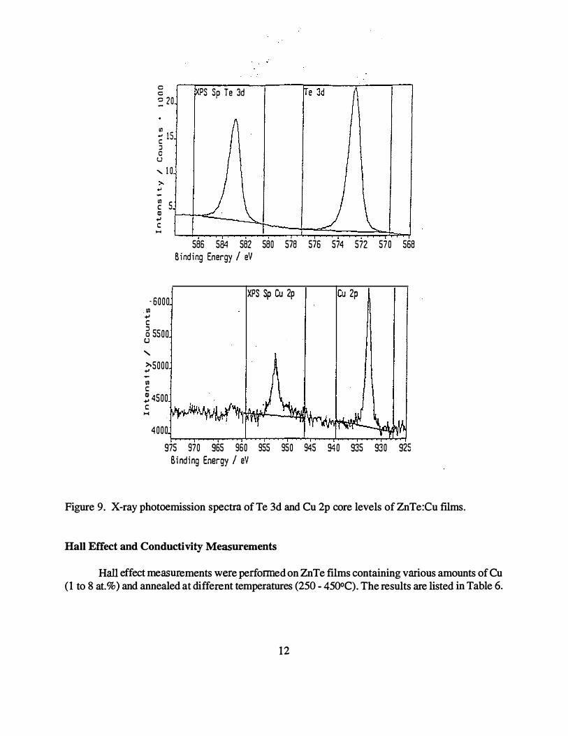
We have performed x-ray photoemission spectroscopy measurements on the ZnTe:Cu films to understand the oxidation states of the Cu dopants. Figure 9 shows the Te 3d and Cu 2p core level photoemission spectra. We do not see any chemical shifts or broadening in either core levels. The binding energy of the Cu 2p lines is in agreement with a Cu• assignment.
11
g PS Sp Te 3d= 20
IJ) .- lS c :J 0 u ...... 10
-� 5! r--+-::::::::::.._ __ --...:� c ....
586 584 582 580 578 576 574 572 570 568
-6000 Ill +' c 5 5500 u
' �5000 -Ul c !! 4500c .....
4000
Binding Energy I eV
XPS Sp Cu 2p u 2p
�������--��������� 975 970 965 960 955 950 945 940 935 930 925
Binding Energy I eV
Figure 9. X-ray photoemission spectra of Te 3d and Cu 2p core levels of ZnTe:Cu films.
Hall Effect and Conductivity Measurements
Hall effect measu rements w ere pe rfo nned on ZnTe films containing v arious amounts ofCu (1 to 8 at.%) and annealed at different temperatures (250 - 450°C). The results are listed in Table 6.
12

Table 6. The dependence of film resistivity, sheet resistance, carrier concentration and mobility of ZnTe as a function of Cu concentration and post-deposition annealing temperature. The fi lm thickness was 0.8 Jlm.
Nominal Cu Annealing R p Mobility Doping
concentration Temperature (OC) (Q/sq) ( !l-cm) ( cm2 N.s) (cm-3)
1% 250 4.8x1()8 3.8x1{)4 6.9 2.4xl013 300 8.0x1{)4 6.4 6.7 1.5xl017 350 9.0x1Q3 0.72 20 4.5xl017 400 1.5x1{)4 1.2 21 2.5xl017 450 1.8x10S 14.0 18 2.6x10¹⁶
2% 250 4.7x1{)4 3.8 0.1 1.4x10¹⁹ 300 4.0xl03 0.32 2.8 7.0xl018
350 1.8x1Q3 0.14 8.6 5.1x10¹⁸
400 3.6x1Q3 0.29 13 1.7x10¹⁸
450 6.8x1Q3 0.55 1.5 7.6x10¹⁸
3% 250 1.6x1{)4 1.3 1.7 2.9x10¹⁸
4% 300 3.0x1Q3 0.24 0.3 7.7xl019 350 1.2xl03 0.10 1.2 5.4xl019 450 2.3x1{)4 1.8 1.9 1.8x1Qts
6% 250 3.4x1{)4 2.7 1.1 2.2xl018
300 150 0.012 1.4 3.8xlQ2° 350 510 0.041 1.0 1.5x1Q20 400 990 0.079 0.6 1.3xlQ2° 450 690 0.055 2.3 4.9x10¹⁹
8% 250 3.3x1{)4 2.6 1.1 2.2x10¹⁸
We can observe several features from Table 6: 1. The lowest resistivity was obtained at an annealing temperature of 350oC. At higher
annealing temperatures, the resistivity increases again. In most cases, the increase of resistivity at high annealing temperature was caused by a decrease of carrier concentration.
2. Very high mobility (for polycrystalline p-type ZnTe) was obtained at low (1 to 2 at. %)Cu doping and relatively low annealing temperatures (350oC). With increase in Cu concentration, the mobility decreases, caused possibly by increased scattering by ionized impurities.
3. 2.0 at. % seems to be the lowest Cu doping that can yield a p-type doping concentrationof over 1018 cm-3• At even lower Cu concentration (0.5 - 1.0 at.%), charge compensation led to very low doping concentration .
13

4. The highest Cu doping efficiency was obtained at a Cu concentration of 6 at. % for filmsannealed at high temperatures. For films annealed at a low temperature (2500C). however, the highest doping efficiency was obtained with a Cu concentration of 2 at. %. As shown in the table, the carrier concentration of both 2 at. % and 3 at. % doped films is higher than that of 6 at. % and 8 at. % doped films for the annealing temperature of 2500C. Since low annealing temperature is desired for back contact formation on CdTe, this result suggests that a Cu doping of 2 at. % is preferable.
The conductivities of the films were measured as a function of temperature following annealing under different conditions. A typical result is shown in Figure 10 for a film doped with 2 at. % of Cu. A peak in resistivity was observed in the temperature range between 130 OC and
. 150 OC. consistent with our previous results obtained with films doped with higher Cu concentration. This peak disappears after 300 OC annealing.
0
IC Cu:2%
1.8 2 2.2 2.4 2.6 2.8 1 ooorr (1/K)
3 3.2 3.4
Figure 10. Temperature dependence of dark conductivity of a ZnTe film doped with 2 at. % of Cu.
The activation energy of the conductivity ofZnTe films was deduced from the temperature dependence of dark conductivity between 2� 120°C. The results are shown in Table 7. We observe several features:
1. The activation energy of conductivity is rather high (0.6 eV) for the undoped film. Theionization energy of the second level of a Zn-vacancy is a possible interpretation for this activation energy [4].
2. For Cu-doped films, the activation energy is smaller than that of the undoped film anddecreases with increasing Cu concentration and annealing temperature. In general, the activation
14
l

energy observed was between 0.2 and 0.5 eV. These values correspond well with the ionization energy reported for intrinsic defect levels in ZnTe (0.25 eV, and 0.5 eV) and are higher than the ionization energy of the Cuzn acceptor level (0.12, 0.15 eV) [5l This indicates that intrinsic defects (e.g., Zn vacancies) are the dominant acceptors. This can be correlated with the compositional analysis results. As discussed in a previous section, there is a high degree of cation deficiency in low Cu-doped films. This may lead to a high concentration of Zn vacancies. It is possible that the main effect of Cu was to create this cation deficiency rather than acting as an acceptor directly. If this is indeed the case, it may be possible to form Zn-deficient ZnTe films using other mechanisms, thereby eliminating Cu completely.
Table 7. Activation energy of dark conductivity of ZnTe films as a function of Cu concentration and post-deposition annealing temperature.
Cu Concentration Annealing Temp. (<C)
0% 300
1.0% 145 235 305
2.0% 140 230 300
3.0% 140 225 305
4.5% 145 190 310
Activation Energy (eV)
0.60
0.45 0.50 0.41
0.40 0.45 0.30
0.42 0.32 0.22
0.25 0.21 0.22
Optimization of ZnTe contact formation on GPI and SCI CdTe/CdS films
CdS/CdTe solar cells were fabricated with ZnTe films containing low Cu concentrations. Both electrodeposited CdTe films prepared at CSM and films prepared elsewhere (Solar Cells, Inc. and Golden Photon, Inc.) using other techniques were used. Good ohmic contacts were obtained on all films using Cu concentrations as low as 1.0 at. %.
(a) GPI samples
Two types of CdTe/CdS films were provided by GPI: regular and recrystallized (sample
15
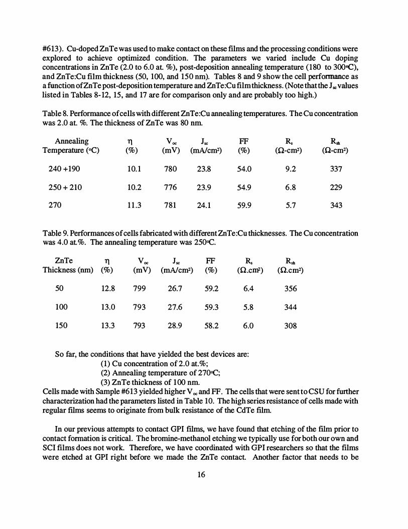
#613). Cu-doped ZnTe was used to make contact on these films and the processing conditions were explored to achieve optimized condition. The parameters we varied include Cu doping concentrations in ZnTe (2.0 to 6.0 at. %), post-deposition annealing temperature (180 to 300<C), and ZnTe:Cu film thickness (50, 100, and 150 nm). Tables 8 and 9 show the cell performance as a function ofZnTe post-deposition temperature and ZnTe:Cu film thickness. (Note thatthe J sc valueslisted in Tables 8-12, 15, and 17 are for comparison only and are probably too high.)
Table 8. Performance of cells with different ZnTe:Cu annealing temperatures. The Cu concentration was 2.0 at. %. The thickness of ZnTe was 80 nm.
Annealing 11 Voc Jsc FF R. Rsh Temperature (oC) (%) (mV) (mA/cm2) (%) (Q-cm2) (0-cm2)
240 +190 10. 1 780 23.8 54.0 9.2 337
250 + 210 10.2 776 23.9 54.9 6.8 229
270 1 1 .3 781 24.1 59.9 5.7 343
Table 9. Performances of cells fabricated with differentZnTe:Cu thicknesses. The Cu concentration was 4.0 at.%. The annealing temperature was 250oC.
ZnTe 11 Voc Jsc FF R. Thickness (nm) (%) (mV) (mA/cm2) (%) (Q.cm2)
50 12.8 799 26.7 59.2 6.4
100 13.0 793 27.6 59.3 5.8
150 13.3 793 28.9 58.2 6.0
So far, the conditions that have yielded the best devices are: (1) Cu concentration of 2.0 at.%; (2) Annealing temperature of 270oC; (3) ZnTe thickness of 100 nm.
R.h (Q.cm2)
356
344
308
Cells made with Sample #613 yielded higher V oc and FF. The cells that were sent to CSU for furthercharacterization had the parameters listed in Table 10. The high series resistance of cells made with regular films seems to originate from bulk resistance of the CdTe ftlm.
In our previous attempts to contact GPI films, we have found that etching of the ftlm prior to contact formation is critical. The bromine-methanol etching we typically use for both our own and SCI films does not work. Therefore, we have coordinated with GPI researchers so that the films were etched at GPI right before we made the ZnTe contact. Another factor that needs to be
16
!

considered is the porous film structure and rough surface of GPI samples. It was necessary to ensurethat the whole surface was contacted. For this purpose, we used graphite, Ag paint, and an In foil pad to contact the ZnTe:Cu films. However, no effects were apparent.
Table 10. Performance of cells fabricated with ZnTe contacts on GPI films.
Sample
#613
regular
(b) SCI samples
11 (%)
14.0
13.0
Voc (mV)
816
793
27.6
27.6
FF (%)
62.0
59.3
R. (Q-crri)
5.2
5.8
347
344
Optimization of ZnTe contact on SCI CdTe/CdS films included optimization of Cu concentration and ZnTe post-deposition annealing temperature. The CdTe surface was etched with 0. 1% (by volume) bromine-methanol solution for 10 s. The results for various Cu dopingconcentrations and ZnTe post-deposition annealing temperatures are summarized in Tables 1 1 and 12.
Table 1 1 . Optimization of Cu concentration in ZnTe for SCI CdTe/CdS films.
Cu 11 Voc Jsc FF Concentration (%) (V) (mA/cm2) (%)
1 .0% 1 1 .6 0.74 23.8 65.6 2.0% 12.4 0.73 24.8 68.0 3.0% 1 1 .6 0.77 23.3 65.0 4.5% 12.2 0.76 24.0 67.0
Table 12. Cell performance as a function of ZnTe post-deposition annealing temperature. The Cu concentration was 2.0 at.%, ZnTe film thickness was 50 nm.
Annealing 11 Voc Jsc FF R. Temp. (OC) (%) (mV) (mA/cm2) (%) (Q-cm2)
200 1 .8 532 9.4 36 20.1270 13.3 796 23.9 70 4.50 280 12.1 763 23.2 68 4.75 350 7. 1 678 20.7 50 18.8
17

The conditions that yielded best devices are: (a) Cu concentration of2.0 at.%; (b) annealing temperature of 270 oC.
Mechanism and Stability Studies
In order to probe any possible Cu diffusion from the ZnTe:Cu film into the CdTe, wemeasured the doping density in the CdTe layer using capacitance-voltage measurements. If Cu does diffuse into the CdTe during the cell fabrication, it would act as an acceptor in the CdTe and higher doping in CdTe would be expected for cells made with ZnTe films containing higher concentrations of Cu or annealed at higher temperatures. As shown in Table 13, there is no obvious correlationbetween CdTe doping density and Cu doping level in the ZnTe.
Table 13. Effect of Cu concentration in ZnTe on the doping density and depletion width of CdTe deduced from capacitance-voltage measurements of cells.
Cu Concentration Doping Density Depletion Width in ZnTe in CdTe (cm·3) (Jlm)
1 .0% 4.2xl014 1 .8
2.0% 5.0xl014 1 .6
3.0% 4.3xlOI4 1 .6
4.5% 2.1xl014 2.3
We also measured the doping density of CdTe as a function of ZnTe post-deposition annealing temperature. As shown in Table 14, we found that higher ZnTe:Cu annealing temperature leads to a higher doping density in CdTe, suggesting Cu diffusion into CdTe layer. We also found that for an annealing temperature of 300 OC, the region closer to the CdTe/Zn Te interface has higher doping density. No such a distinct region was observed in cells fabricated at lower annealing temperatures.
Table 14. CdTe doping density as a function of annealing temperature. The Cu concentration was 2.5 at. %
Sample Annealing Temperature Doping in CdTe
44gpi#1 240 OC+ 190 OC 3.9x10¹⁴ 44gpi#2 2500C+210 oc 5.3xl014 44gpi#3 270 0C 1 .0x1015 45gpi#4 300 oc 4.3x10¹⁵
18
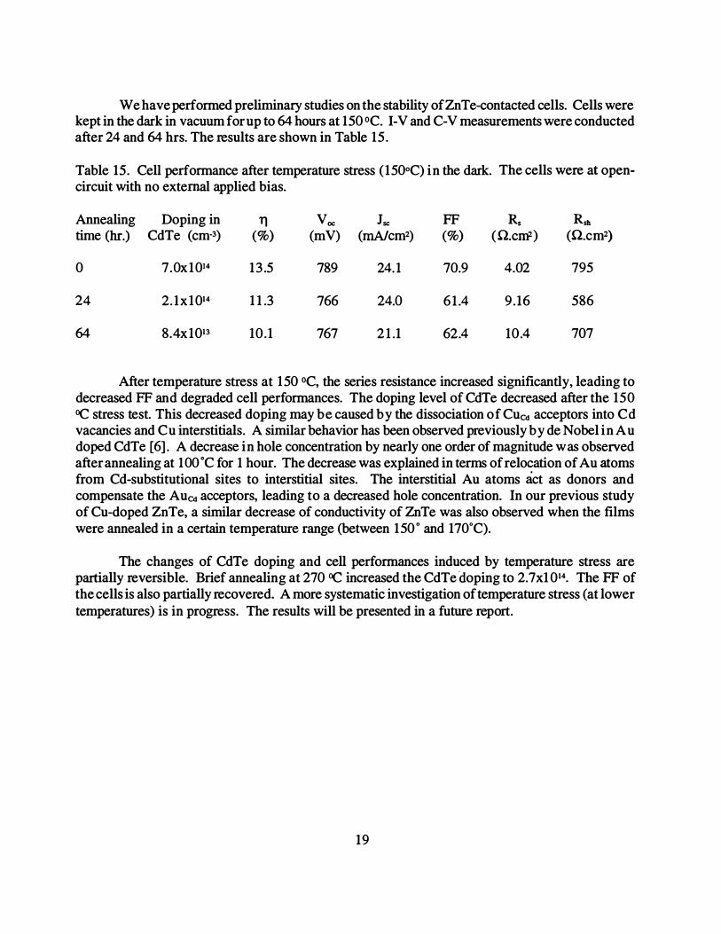
We have performed preliminary studies on the stability ofZnTe-contacted cells. Cells were kept in the dark in vacuum for up to 64 hours at 150 °C. 1-V and C-V measurements were conductedafter 24 and 64 hrs. The results are shown in Table 15.
Table 15. Cell performance after temperature stress (150oC) in the dark. The cells were at open-circuit with no external applied bias.
Annealing Doping in , Voc Jsc FF Rs Rsh time (hr.) CdTe (cm·3) (%) (mV) (mA/cm2) (%) (Q.cm2) (Q.cm2)
0 7.0x10¹⁴ 13 .5 789 24.1 70.9 4.02 795
24 2. 1x10¹⁴ 1 1 .3 766 24.0 61 .4 9.16 586
64 8.4x10¹³ 10.1 767 21 .1 62.4 10.4 707
After temperature stress at 150 °C, the series resistance increased significantly, leading to decreased FF and degraded cell performances. The doping level of CdTe decreased after the 150OC stress test. This decreased doping may be caused by the dissociation of CuCd acceptors into Cd vacancies and Cu interstitials. A similar behavior has been observed previously by de Nobel in Au doped CdTe [6] . A decrease in hole concentration by nearly one order of magnitude was observed after annealing at 100 ·c for 1 hour. The decrease was explained in terms of relocation of Au atomsfrom Cd-substitutional sites to interstitial sites. The interstitial Au atoms act as donors and compensate the AuCd acceptors, leading to a decreased hole concentration. In our previous study of Cu-doped ZnTe, a similar decrease of conductivity of ZnTe was also observed when the films were annealed in a certain temperature range (between 150• and 170.C).
The changes of CdTe doping and cell performances induced by temperature stress are partially reversible. Brief annealing at 270 OC increased the CdTe doping to 2. 7x1 014• The FF ofthe cells is also partially recovered. A more systematic investigation of temperature stress (at lower temperatures) is in progress. The results will be presented in a future report.
19

4. Fabrication of CdTe/CdS cells on TiO:·coated Sn02 substrates
We participated in team work in expl oring the effect ofTi92 as an intrinsic layer on the SnO::substrates. The TiO::: and SnO::: films were grown by the Harvard group and the USF group, respectively. The intention was to test if Ti02 would be more effective in preventing shuntingassociated with pinholes in CdS. The conduction band offset at the CdS/oxide interface is also expected to be smaller because of the lower electron affinity of Ti02•
We found that the TiO:� film is too resistive for the electrodeposition of CdTe. The CdTe films show very po o r adhesion and peel off during the depositi on or post-deposition annealing. By modifying our annealing procedure, we were able to fabricate cells with limited success. The light 1-V curves of cells fabricated with several CdS thicknesses on the TiO:/SnO::/glass substrates areshown in Figure 1 1 . ·
<.§.c: � :; ()
3-----------------,
2
0 0.0 0.2
0.6
0.5
0.4
0.3
0.2
0.1
No CdS Voc= 0.85 V J,.,= 20.8 mA/cm2
FF = 0.21 Efficiency = 3.5%
0.4 0.6
Voltage M
o.s
CdS: 1900 angstrom Voc= 0.65 V Joe= 14.2 mA/cm2
FF = 0.13 Efficiency = 1 .2%
1 .0
0.0 4--.--,-----.--,--�::::.:---.---.--..--J 0.0 0.1 0.2 0.3 0.4 0.5 0.6 0.7 0.8 0.9 1 .0 .
Voltage (V)
20
3.-------------------,
2
CdS: 560 angstrom Vee= 0.82 V Joe = 22.4 mA/c:n2
FF = 0.12 Efficiency = 2.3%
0 4----,------,----=;==---.---� 0.0 0.2 0.4 0.6 0.8 1 .0
Voltage M
Figure 11. Light 1-V curves of CdTe/CdS cellsfabricated on Ti{h-coated SnQ substrates.
From Figure 1 1 , we notice that cells with no CdS showed the highest efficiency. The V oc value of 0.84 - 0.85 e V is very high for electrodeposited CdTe. The photocurrent is also reasonable. The very poor fill factor was caused by the high resistance ofTi02• The high V oc and Jsc indicate that Ti02 may be a good candidate for the intrinsic layer between Sn02 and CdS or as the heterojunction partner with p-type CdTe. The low fill factor may be improved by doping of the Ti02 film.
Other Team Activities
For the thin CdS team activity, we have prepared CdTe/CdS cells using different CdS thicknesses on Sn02 substrates provided by USF. The CdS thicknesses, treatment conditions, and the photovoltaic performance of the cells studied are presented in Tables 16 and 17.
Table 16. The CdS thickness and post-deposition treatment conditions
Sample # CdS thickness CdCh-treatment of CdS
A 85 nm No B 45 nm No c 45 nm Yes D 85 nm Yes
Table 17. The photovoltaic performance of the cells listed in Table 16
Sample Voc (V)
A 0.70 B 0.71 c 0.66 D 0.70
Jsc (mA/cm2)
24.5 25.0 25.8 26.0
FF
0.59 0.59 0.48 0.59
Efficiency (%)
10.0 10.4 8.2
10.5
Because of the CdS consumption during final annealing of CdTe/CdS films, the final CdS thickness is much smaller than the nominal thickness listed in Table 16. The cells fabricated with very thin and CdCl2-treated CdS showed much lower Vox and fill factor, presumably caused by shunting. This was expected because of the CdS grain growth during CdC12-treatment which is likely to lead to the formation of pinholes.
21

6. Summary
During the past year, we have performed systematic studies of the growth and properties of electrodeposition CdS and back contact formation using Cu-doped ZnTe with an emphasis on low Cu concentrations. We have also started to explore the stability of our ZnTe-Cu contacted solar cells.
We have investigated the electrodeposition of CdS and its application in fabricating CdTe/CdS solar cells. The experimental conditions we explored in this study were: pH from 2.0 to 3.0; temperatures of 80° and 900C; CdC12 concentration of 0.2 M; deposition potential from -550 to -600 mV vs. Ag/AgCl electrode; [Na2S204] concentration between 0.005 and 0.05 M. The deposition rate increases with increase of the thiosulfate concentration and decrease of solution pH. We also observed that the acid used to adjust the pH has a large impact on the deposition rate. The deposition is faster in a hydrochloric acid solution than in a sulfuric acid solution. The surface morphology of electrodeposited CdS thin films was investigated using scanning electron microscopy. The most pronounced difference in film morphology was observed for different solution temperatures. Films deposited in a hydrochloric acid solution at 800C consist of agglomerates of small crystallites. These agglomerates have a rather uniform size of - 0.7 J.lm and
cover the tin oxide substrates uniformly. Films deposited at a higher temperature of 90°C are nonuniform with J.lm-size CdS agglomerates covering only a small portion of the substrates.
Therefore, in terms of film uniformity and cell fabrication, deposition in a hydrochloric acid solution at 800C is preferred. The improved uniformity can be related to the slow growth rate obtained under such conditions. CdTe/CdS cells were prepared using electrodeposited and physical vapor deposited CdTe on electrodeposited CdS. Moderate cell efficiencies were obtained in the preliminary study.
We have extended our preyious research of ZnTe:Cu films by investigating films doped with low Cu concentrations (<5.0 at. %). The low Cu concentration enabled us to increase the Zn Te:Cu post -annealing temperature without causing excessive Cu diffusion into CdTe or formation of secondary phases. The effects of Cu doping concentration and post-deposition annealing temperature on the structural, compositional, and electrical properties of ZnTe were studied systematically using x-ray diffraction, atomic force microscopy, electron microprobe, Hall effect and conductivity measurements. XRD measurements indicated that the crystalline phase of asdeposited and low-temperature annealed ZnTe films is dependent on Cu doping concentration. LowCu-doped films exhibited zincblend phase, whereas high-Cu-doped films showed wurtzite phase.After annealing at high temperature ( ;:;::3500C), all films exhibited zincblend structure. Electron probe microanalysis revealed a deficiency of cations in low-Cu-doped films and an excess of cations in high-Cu-doped films. Hall effect measurements revealed a dependence of hole mobility on Cu doping concentration with the highest mobility (20 cm2N s) obtained at a low Cu concentration of2 at.% and relatively low annealing temperatures. Studies of the activation energy of dark conductivity suggested that intrinsic defects (e.g., Zn vacancies) are the dominant acceptors for Cu concentrations lower than 4.5 at.%. Finally, ZnTe films with Cu concentrations as low as 1 at. % were used successfully as a back contact layer in CdTe based solar cells. Fill factors over 0. 70 were obtained using films of low Cu doping.
22

7. Acknowledgements
We thank the scientists at the National Renewable Energy laboratory (NREL) for various measurements, especially David Niles for XPS measurements, Alice Mason for electron probe microanalysis, and Helio Moutinho for atomic force microscopy measurements. We thank the NREL CdTe team members: Peter Sheldon, David Albin, Xiaonan Li, Tim Gessert, and Doug Rosefor many helpful discussions and experimental help. We thank Brian McCandless of the Institute of Energy Conversion, the University of Delaware for pinhole density survey and cell fabricationon electrodeposited CdS films and high temperature treatment of electrodeposited CdTe ftlms. The investigation of the effects of CdS film thickness and Ti02 coating on cell performances and back contact optimization on SCI and GPI films were part of a coordinated effort of the Thin Film Photovoltaic Partnership team. Chris Ferekides of the University of South Florida provided Sn02- coated glass substrates. Roy Gordan of Harvard University deposited the Ti02 layer. Solar Cells, Inc. and Golden Photon, Inc. provided CdTe/CdS films prepared by sublimation and spray pyrolysis. Finally, we thank Kenneth Zweibel and Bolko von Roedem of NREL for helpful discussions and encouragement.
8. References
� ' J . Tang, D. Mao, L. Feng, W. Song, and J.U. Trefny, Proc. 25th IEEE Photovoltaic Specialists Gpnference, 1996, pp. 925-928.
· · ..::
. -�! .. .,.. ��·�· J. Tang, L.,Feng, D. Mao, W. Song, Y. Zhu, and J.U. Trefny, Mater. Res. Soc. Symp. Proc. 426, 1996, pp. 355-360 .
:f;T.A. Gessert, A.R. Mason, R.C. Reedy, R. Matson, T.J. Coutts, and P. Sheldon, J. Electronic Jr!aterials, Vol. 24, p. 1443 (1995); T.A. Gessert, A.R. Mason, P. Sheldon, A.B. Swartzlander, D.Niles, and T.J. Coutts, J. Vac. Sci. & Technol. Vol. A14, p.806 (1996).
4. T.L. Larsen, C.F. Varotto, and D.A. Stevenson, J. Appl. Phys. 43, 172 (1972).
5. H. Tubota, Jap. J. Appl. Phys. 2, 259 (1963); M. Aven, and B. Segall, Phys. Rev. 130, 81 (1963).
6. D. de Nobel, Phillips Res. Rep. 14, 430 (1959)
23

9. Appendices
9.1. Personnel
Many individuals contributed to this work. Their names, titles, and representative responsibilities are summarized below.
John U. Trefny, Professor of Physics: Project Coordinator.
Duli Mao, Research Assistant Professor: Photovoltaic Development.
Don L. Williamson, Professor of Physics: Structural Properties of Materials.
Reuben T. Collins, Professor of Physics: Electronic and Optical Properties of Semiconductors.
Thomas E. Furtak, Professor of Physics: Electrochemistry, Optical Properties.
Timothy R. Ohno, Assistant Professor of Physics: Surface Physics.
Yuming Zhu, Graduate Research Assistant: CdS Chemical Bath Deposition.
Wenjie Song, Graduate Research Assistant: CdTe Electrodeposition and Cell Optimization.
Jian Tang, Graduate Research Assistant: ZnTe Back Contact, Cell Fabrication, and Stability.
Figen Kadirgan, Visiting Professor: Electrodeposition of CdS.
Sana Kutun, Visiting Graduate Student: Electrodeposition of CdS.
M. Hasan Asian, Graduate Student: Photoluminescence.
Ahmed Alkaoud, Graduate Student: Transparent Conducting Oxide.
Troy Berens, Graduate Student: Copper Indium Diselenide Thin Film Solar Cells.
Ahmed Balcioglu, Graduate Student: Surface Analysis and Deep Level Transient Spectroscopy.
24

9.2. Laboratory Improvements
1 . A major laboratory renovation project was finished during the past year. This laboratory renovation project was supported by the Infrastructure Program ofNational Science Foundation with matching funds from the School of Mines. The total investment of NSF and CSM in this new facility exceeded $800,000 and provided a new 2,200 sq. ft . thin film processing laboratory with 3 more filtered fume hoods, a class-1 ,000 clean room, ample lab space, and other hardware related to the safety of staff members and students. During the renovation, efforts were made to minimize the disruption of the construction work to the CdTe project.
2. A proposal for the "Acquisition of Characterization Instrumentation for AdvancedMaterials Research" to the Infrastructure (Instrumentation) Program of NSF was granted. This allowed us to acquire 4 pieces of equipment that are critically important for our thin film research: a Ten cor P-1 0 surface profiler with three-dimensional imaging capability, a Cary 5G UV-Vis-NIRspectrophotometer with diffuse reflection accessory, a variable temperature Hall effect measurement station, and a three-wavelength (633, 830, 1300 nm) ellipsometer. In addition, Professor Ohno has acquired an x-ray photoemission spectroscopy system, also sponsored by the Infrastructure (Instrumentation) Program of NSF. These new instruments have all arrived and are functioning. This is expected to greatly facilitate our CdTe thin films research.
For the infrastructure projects listed above, the Colorado School of Mines has provided about $800,000 in matching funds, demonstrating clearly its strong commitment to thin films and photovoltaics research.
9.3. Publications
"The Structural, Optical, and Electrical Properties of Vacuum Evaporated Cu-doped ZnTe Polycrystalline Thin Films", L.H. Feng, D. Mao, J. Tang, R. Collins, and J.U. Trefny, J. Electron. Materials 25,1433 (1996).
"Effect of Annealing on Microstructure, Residual Stress, and Photovoltaic Characteristics of Electrodeposited CdTe Films", B. Qi, D. Kim, D.L. Williamson, and J.U. Trefny, J. ofElectrochem. Soc. 143, 517 (1996).
"Effect of CdCiz Treatment of CdS Films on CdTe/CdS Solar Cells", W. Song, D. Mao, L. Feng, Y. Zhu, M.H. Asian, R.T. Collins, and J.U. Trefny, Mater. Res. Soc. Symp. Proc. 426, 1996, pp. 331-336.
"Study ofZnTe:Cu Back Contacts on CdTe/CdS Thin Film Solar Cells", J. Tang, L. Feng, D. Mao, W. Song, Y. Zhu, and J.U. Trefny, Mater. Res. Soc. Symp. Proc. 426, 1996, pp. 355-360.
"Chemical Bath Deposition of CdS Thin Films: Growth and Structural Studies", Y. Zhu, D. Mao, D.L. Williamson, and J.U. Trefny, Mater. Res. Soc . Symp. Proc. 426, 1996, pp. 227-232.
25
"Fabrication of CdTe Thin Film Solar Cells Using Electrodeposition", W. Song, D. Mao, Y. Zhu,J. Tang, and J.U. Trefny, Proc. 25th IEEE Photovoltaic Specialists Conference, 1996, pp. 873-876.
"The Properties and Optimization ofZnTe:Cu Back Contacts on CdTe/CdS Thin Film Solar Cells", J. Tang, D. Mao, L. Feng, W. Song, and J.U. Trefny, Proc. 25th IEEE Photovoltaic Specialists Conferenc� 1996, pp. 925-928.
"Effect of Cu Doping on the Properties of ZnTe:Cu Thin Films and CdS/CdTe/ZnTe Solar Cells", J. Tang, D. Mao, and J. U. Trefny, Proc. 14th NREL Photovoltaic Program Review Meeting, 1996, pp.639-646.
26
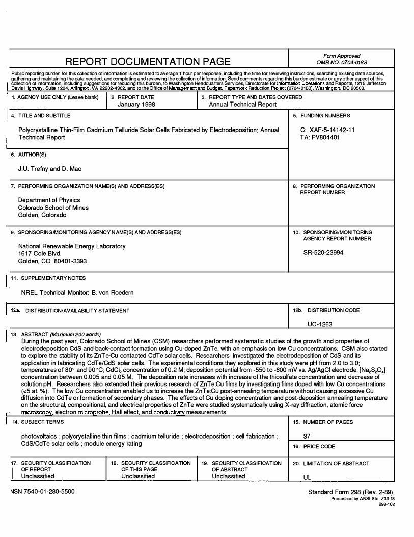
REPORT DOCUMENTATION PAGE Form Approved OMB NO. 0704-0188
Public reporting burden for this collection of information is estimated to average 1 hour per response, including the time for reviewing instructions, searching existing data sources, gathering and maintaining the data needed, and completing and reviewing the collection of information. Send comments regarding this burden estimate or any other aspect of this
I collection of information, including suggestions for reducing this burden, to Washington Headquarters Services, Directorate for lnfo�ation Op��tions and Reports, 1 21 5 Jefferson Davis HiQhwav. Suite 1 204, ArlinQton, VA 22202-4302, and to the Office of ManaQement and BudQet, Paperwork Reduction Project 0704-0188 , WashinQton, DC 20503. 1. AGENCY USE ONLY {Leave blank) 2. REPORT DATE 3. REPORT TYPE AND DATES COVERED
January 1 998 Annual Technical Report
I 4. TITLE AND SUBTITLE 5. FUNDING NUMBERS
Polycrystalline Thin-Film Cadmium Telluride Solar Cells Fabricated by Electrodeposition; Annual C: XAF-5-141 42-1 1
I Technical Report TA: PV804401
6. AUTHOR{S)
J.U. Trefny and D . Mao
7. PERFORMING ORGANIZATION NAME{S) AND ADDRESS{ES) 8. PERFORMING ORGANIZATION REPORT NUMBER
Department of Physics Colorado School of Mines Golden, Colorado
I I 9. SPONSORING/MONITORING AGENCY N AME{S) AND ADDRESS{ES) 10. SPONSORING/MONITORING
AGENCY REPORT NUMBER
National Renewable Energy Laboratory 1 6 1 7 Cole Blvd. SR-520-23994
Golden, CO 80401 -3393
I 1 1 . SUPPLEMENTARY NOTES
NREL Technical Monitor: B. von Roedern
l 12a. DISTRIBUTION/AVAILABILITY STATEMENT 12b. DISTRIBUTION CODE
UC-1 263 1 13. ABSTRACT (Maximum 200 words) During the past year, Colorado School of Mines (CSM) researchers performed systematic studies of the growth and properties of
I
I
I
electrodeposition CdS and back-contact formation using Cu-doped ZnTe, with an emphasis on low Cu concentrations. CSM also started to explore the stability of its Zn T e-Cu contacted CdT e solar cells. Researchers investigated the electrodeposition of CdS and its application in fabricating CdTe/CdS solar cells. The experimental conditions they explored in this study were pH from 2.0 to 3.0; temperatures of sao and 90°C; CdC� concentration of 0.2 M; deposition potential from -550 to -600 mV vs. Ag/AgCI electrode; [N�Sp4] concentration between 0.005 and 0.05 M. The deposition rate increases with increase of the thiosulfate concentration and decrease of solution pH. Researchers also extended their previous research of ZnTe:Cu films by investigating films doped with low Cu concentrations (<5 at. %). The low Cu concentration enabled us to increase the ZnTe:Cu post-annealing temperature without causing excessive Cu diffusion into CdTe or formation of secondary phases. The effects of Cu doping concentration and post-deposition annealing temperature on the structural, compositional, and electrical properties of ZnTe were studied systematically using X-ray diffraction, atomic force microscopy, electron microprobe, Hall effect, and conductivity measurements.
14. SUBJECT TERMS 15. NUMBER OF PAGES
photovoltaics ; polycrystalline thin films ; cadmium telluride ; electrodeposition ; cell fabrication ; CdS/CdTe solar cells ; module energy rating
17. SECURITY CLASSIFICATION 18. SECURITY CLASSIFICATION 19. SECURITY CLASSIFICATION OF REPORT OF THIS PAGE OF ABSTRACT Unclassified Unclassified Unclassified
\JSN 7540-01 -280-5500
16.
20.
37
PRICE CODE
LIMITATION OF ABSTRACT
UL
Standard Form 298 (Rev. 2-89) Prescribed by ANSI Std. Z39-18
298-102