i know what i did this summer… attend the summer ret research program at fiu flagler campus. dr....
TRANSCRIPT

I know what I did this summer…
• Attend the summer RET research program at FIU Flagler campus.
Dr. Masoud Milani
Stephanie Strange
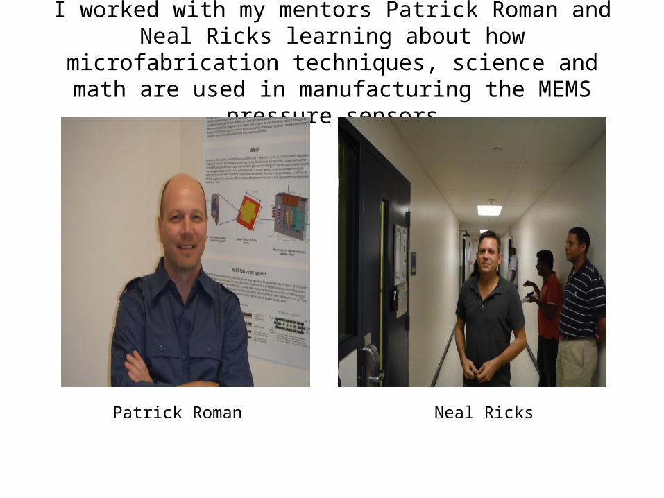
I worked with my mentors Patrick Roman and Neal Ricks learning about how microfabrication techniques, science and math are
used in manufacturing the MEMS pressure sensors
Patrick Roman Neal Ricks

Made a really cool poster on the MEMS pressure sensor
Take the Pressure Sensor Challenge
1. How does the sensor detect a change in voltage?
2. What do we call the process of creating thin layers on a silicon wafer?
3. Why is Nickel used to build the Wheatstone configuration?
4.What metals determine what charge the bare silicon wafer will carry?
5. Place the images on the right in the correct order of the fabrication process.
Special Acknowledgments to:Masoud Milani, Stephanie Strange , Patrick Roman and everyone at FIU Flagler campus for making the summerRET program a reality.
www.periodictable.com
c
FIU ENGINEERINGRET SUMMER PROGRAM
Micro Electrical Mechanical Systems (MEMS) Pressure SensorCarlos Hernandez, Patrick Roman, Neal Ricks, Dr. Nezih Pala, Masoud Milani
Manufacturing the Pressure sensor The FIU department of Engineering and Computer Science with the Motorola Nanofabrication Research Facility at FIU’s Flagler campus use micro fabrication processes to get the job done. The MEMS pressure sensor is a classic example of micro engineering today, it consists of a Wheatstone bridge sensor configuration on a silicon nitride membrane. The pressure sensor is activated when changes in resistance across the silicon nitride membrane takes place due to changes in pressure. The sensor can be used in a variety of applications from your phones microphone to your cars intake manifold.
When pressure is applied to the silicon nitride membrane the variable resistors elongate and create a change in voltage. This change in voltage can be used to send signals and commands to electronic devices. Silicon nitride is selected as the membrane material due to its microfabrication compatibility and robust mechanical properties.
A Wheatstone bridge is a circuitry pattern used in microfabrication processes. R1 and R4 represent the variable resistors , R2 and R3 are constant resistors . The variable resistors are placed on the silicon nitride membrane to measure changes in pressure.
N. Pala Mems Lecture
1. Pure silicon crystals doped with Boron (P) or Phosphorus (N) are cut and polished into 4 inch wafers that are 675 micrometers thick. The dopant determines the charge. 2. Deposition of Nitrogen across the wafer using thermal oxidation follows. This deposits a thin film of silicon nitride on both sides of the wafer. 3.Photolithography techniques are used to layer the front of the wafer. This layering creates the pattern for the Wheatstone bridge configuration. a. Frontside Photolithography - Coatb. Frontside Photolithography -Exposec. Frontside Photolithography -Develop
4. Metal deposition of chromium and Nickel are used to form the pattern for the Wheatstone bridge contacts and resistors. These metals are deposited into the patterns created during the frontside photolithography processes. An evaporator deposits 100 angstroms of Chromium and 4000 angstroms of Nickel on to the wafer. Chromium is used for its bonding properties with silicon nitride and Ni for its conducting properties. An acetone bath is used to remove excess metal deposition. Excess resist is also removed here with developer solutions, LOR. 5. The backside of the wafer is then processed with photolithography processes as well. This is how the back side of the wafer is shaped. It also follows a three step process. a. Backside Photolithography Coatb. Backside Photolithography - Exposec. Backside Photolithography - Develop6. Backside patterning of the wafer is done using a Reactive Ion Etcher which uses a plasma to etch out the of silicon nitride layer that remains.7. A piranha bath of sulfuric acid and hydrogen peroxide cleans the wafer to remove any remaining photoresist used in the layering processes of photolithography 8. Finally the silicon nitride on the back side is etched using a heated bath of potassium hydroxide to complete the backside of the wafer.
Photolithography is a microfabrication process which is used to pattern silicon wafers by shining UV light through a patterned mask onto light sensitive chemicals called photo resist. For the mems pressure sensor, two layers of resist are used that develop at different rates. This creates an undercut in the second layer of resist. By creating this undercut metals can be deposited and lifted away leaving behind the Wheatstone bridge pattern.
Photolithography
MEMS Pressure Sensor
a b
c d

Got to see some really cool PowerPoints presentations by Dr. Pala and Dr. Khizroev on microfabrication of the MEMS
pressure sensor and micro technology in fighting cancer
Dr. Sakhrat KhizroevDr. Nezih Pala

Hands on lab activities in building the MEMS pressure sensor

Collaborated with my peers in developing lesson plans geared towards science, technology, science and math
(STEM).

Made some new friends.

That is what I did this summer
• What a great opportunity and learning experience I had this summer. I can take back to the classroom what I learned and engage my students in real world applications of science and engineering.
I had a great time Dr. Milani hope to see you next summer….

The Endby
Carlos HernandezChemistry/ Miami Sunset Senior High