i introduction - wiley-vch · 2008-02-05 · slip casting of ceramics is a technique that has long...
TRANSCRIPT

IIntroduction
j1
Ceramics Science and Technology. Vol.1: Structures. Ralf Riedel and I-Wei Chen (Eds.)Copyright � 2008 WILEY-VCH Verlag GmbH & Co. KGaA, WeinheimISBN: 978-3-527-31155-2

1Modern Trends in Advanced CeramicsRalf Riedel, Emanuel Ionescu, and I.-Wei Chen
1.1Advanced Ceramics
Ceramics are defined as inorganic, non-metallic materials which are typically crys-talline in nature and containmetallic and non-metallic elements such as Al2O3, CaO,ZrO2, SiC, and Si3N4. There are several broad categories of ceramics classifying theindustrial products as follows: clay products, white ware, refractories, glasses, ce-ments, abrasives, and advanced ceramics.Advanced ceramics arematerials tailored to possess exceptional properties (super-
iormechanical properties, corrosion/oxidation resistance, thermal, electrical, opticalor magnetic properties) by controlling their composition and internal structure.They are subdivided into structural ceramics (wear parts, cutting tools, engine com-ponents and bioceramics), electrical ceramics (capacitors, insulators, substrates, in-tegrated circuit packages, piezoelectrics, magnets and superconductors), ceramiccoatings (engine components, cutting tools and industrial wear parts) and chemicalprocessing and environmental ceramics (filters, membranes, catalysts and catalystsupports).As an example of advanced ceramics, silicon carbide (SiC) bearings for chemical
plants are shown in Figure 1.1. This type of device must withstand aggressivechemical environments, show high compressive strength, high stiffness, low den-sity, high fracture resistance, and remain stable under thermal stress.
1.2Conventional Synthesis and Processing of Advanced Ceramics
1.2.1Synthesis of Ceramic Powders
The preparation of ceramic products typically involves heating processes of ceramicpowders which must undergo special handling in order to control purity, particle
j3
Ceramics Science and Technology. Vol.1: Structures. Ralf Riedel and I-Wei Chen (Eds.)Copyright � 2008 WILEY-VCH Verlag GmbH & Co. KGaA, WeinheimISBN: 978-3-527-31155-2

size, particle size distribution, and heterogeneity. These factors play an importantrole in the properties of the finished ceramic part. In principle, it is possible todistinguish finished ceramics made of naturally harvested materials from fullysynthetically prepared starting materials. While most of the binary oxide ceramicssuch as alumina or silica can be processed from natural sources, non-oxide ceramicsand more complex oxides such as high-temperature superconductors must be ob-tained by complex synthetic routes. Both the natural products and the syntheticmaterials must be controlled in terms of their chemical compositions and homoge-neity, specific shape, particle size, and particle size distribution (Figure 1.2).There are several synthetic methods for the preparation of ceramic powders.
Solid-state reactions are the most widely used processes as they are suitable for the
Figure 1.1 High-temperature and corrosion-resistant siliconcarbide (SiC) advanced ceramic (right) produced from siliconcarbide raw material (left) obtained by the reaction of silica withcarbon at temperature >2000 �C, according to the Achesonprocess.
Figure 1.2 SEM image of a sol–gel-derived silicon carbide/nitride-based composite powder. The particle size distribution of thepowder is shown in the inset.
4j 1 Modern Trends in Advanced Ceramics
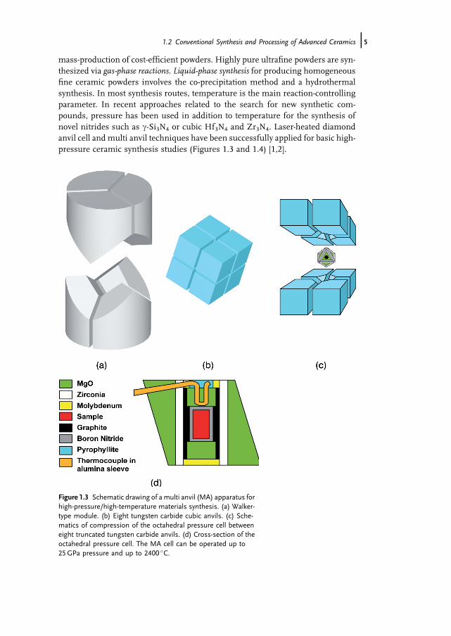
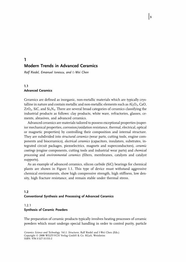
mass-production of cost-efficient powders. Highly pure ultrafine powders are syn-thesized via gas-phase reactions. Liquid-phase synthesis for producing homogeneousfine ceramic powders involves the co-precipitation method and a hydrothermalsynthesis. In most synthesis routes, temperature is the main reaction-controllingparameter. In recent approaches related to the search for new synthetic com-pounds, pressure has been used in addition to temperature for the synthesis ofnovel nitrides such as g-Si3N4 or cubic Hf3N4 and Zr3N4. Laser-heated diamondanvil cell and multi anvil techniques have been successfully applied for basic high-pressure ceramic synthesis studies (Figures 1.3 and 1.4) [1,2].
Figure 1.3 Schematic drawing of a multi anvil (MA) apparatus forhigh-pressure/high-temperature materials synthesis. (a) Walker-type module. (b) Eight tungsten carbide cubic anvils. (c) Sche-matics of compression of the octahedral pressure cell betweeneight truncated tungsten carbide anvils. (d) Cross-section of theoctahedral pressure cell. The MA cell can be operated up to25GPa pressure and up to 2400 �C.
1.2 Conventional Synthesis and Processing of Advanced Ceramics j5
1.2.2Forming
Forming processes involve a mix, slip, or plastic material which is formed into ashape. It is generally desirable to have high green densities, as this factor acts againstthe firing shrinkage. This leads also to reduced rejects and lower firingtemperatures.There are several forming processes for advanced ceramics. Some of these are
classified as traditional, namely die pressing or cold isostatic pressing (CIP). Slipcasting and extrusion, tape casting and injection-molding processes are classified aswet and high-tech forming processes.Die pressing is by far the most frequently used forming process for advanced
ceramics, and involves the uniaxial compaction of a granulated powder duringconfined compression in a die. The pressed green bodies can be then fired directlyor after isostatic pressing.Isostatic pressing involves the shaping of granular powders in a flexible, air-tight
container placed in a closed vessel filled with pressurized liquid. This methodassures a uniform compaction of the powders into a green body that retains thegeneral shape of the flexible container and any internal tooling profile.Slip casting of ceramics is a technique that has long been used for manufacturing
traditional ceramics. The advantages of slip casting include its ability to form greenbodies of a complex shape, without expensive tooling. The bodies produced arealmost invariably thin-walled with a uniform thickness. It is an inexpensive processwhen compared with other ceramicmanufacturing techniques. A slip is prepared byball-milling the appropriate powders along with binders, plasticizers, deflocculants,etc., in a solvent or water. In order to reproduce the castings, it is essential that the
Figure 1.4 Schematic drawing of a laser-heated diamond anvilcell (LH-DAC) for the high-pressure and high-temperature ma-terials synthesis (left). The inset on the right shows the sampleholder device. The LH-DAC can be operated at pressures up to100GPa and 7000 �C. For further details, see Refs. [1,2].
6j 1 Modern Trends in Advanced Ceramics

slip is characterized by means of its viscosity, dilatancy, solids content, etc. Such aslip is poured into a porousmold, where the liquid part of the slip will be absorbed bycapillary action into themold to leave a layer of ceramic and additives formed againstthe plaster. It is possible to improve green density and impart higher green strengthon a cast body by applying an ultrasonic frequency to the mold during casting.Another way to improve green body characteristics is to apply pressure (e.g., by gas)to the slip during casting. This can yield higher densities and minimize shrinkageafter casting.Due to the poor ductility and the high flow stress of ceramics, extrusion process
should be performed under a higher temperature and slower speed than for themetals in order to reduce the flow stress and to avoid fracture.Hot extrusion can be apromising ceramic manufacturing technique if a textured structure is desired.Nevertheless, this method is limited to large cross-section products of non-structuralceramics with a low melting point [3].Tape casting is used for producing, for example, multilayered capacitors, multi-
layered ceramic packages, piezoelectrics, ceramic fuel cells, and lithium ion batter-ies. The advantage of the tape casting method is that it is the best technique forcreating large, thin and flat ceramic parts, which are impossible to produce withother techniques such as pressing or extrusion. In the ceramic industries, theprocess of tape casting is considered comparable to traditional slip casting as italso uses a fluid suspension of ceramic particles as the starting point for processing.Injection-molding is a suitable process for the high-volume production of complex
design parts, and for manufacturing complex precision components with the high-est degree of repeatability and reproducibility. It is a combination of powder, injec-tion-molding and sintering technologies. The injection-molding process has theadvantage that it is a near net shape technique, so that grinding or major externalfinishing of the produced parts is not necessary.
1.2.3Sintering
The sintering process converts the greenmicrostructure to themicrostructure of thedense ceramic component. In this way, sintering is the last of the ceramic processingsteps where the ceramist has an influence on microstructural development. Thisinfluence is limited, however, as the worst inhomogeneities that pre-exist in thecompact are usually exaggerated during sintering; for example, flaws will persist oreven grow, while large particles may induce abnormal grain growth.The sintering process consists of solid particle bonding or neck formation, fol-
lowed by continuous closing of pores from a large open porosity to essentially pore-free bodies. There are various sintering processes which occur by different mechan-isms. Traditional household and sanitary ceramic ware are densified by viscous flow.In contrast, technical or advanced ceramics are produced by liquid-phase and solid-phase sintering, which utilize significantly smaller amounts of sintering additives ascompared to viscous flow densification. Liquid-phase sintering involves solution–reprecipitation and diffusion mechanisms, while solid-state sintering is dominated
1.2 Conventional Synthesis and Processing of Advanced Ceramics j7

by volume and grain boundary diffusionmechanisms responding to free energy andchemical potential differences. Another method of producing advanced ceramics isthe reactive sintering processes. Here, the solid phase precipitates from an interme-diary liquid phase which is generated during compaction. In a recent review, thephenomena associated with sintering have been fundamentally discussed from atheoretical point of view [4].When the particle size of the precursor powders decreases to nanosized powders,
new mechanisms such as grain boundary slip, dislocation motion, grain rotation,viscous flow and grain boundary melting become operative. Furthermore, sinteringof nanopowders enjoys a high driving force and enhanced kinetics due to thecurvature effect. Thus, the densification of nanopowders occurs at temperaturessignificantly below those of larger-grained powders by up to several hundreds ofdegrees. Consequently, small final grain sizes may result and sintering aids andundesirable phase transformation may be avoided.For theenhanceddensificationof ceramic powders, pressure-assisted consolidation
methods such as hot pressing, hot isostatic pressing, sinter forging, hot extrusion orultra-high pressure sintering can be applied. Hot pressing is a technique which com-bines external uniaxial pressure with temperature in order to enhance densification.Hot pressing is only suited to relatively simple shapes, with the products usuallyrequiring subsequent diamond grinding to achieve the finished tolerances. The hotisostatic pressing (HIP) technique combines high temperature and a gas pressure,which is uniformly applied to the powders in all directions. This is used industriallyto produce defect-free castings, complex shaped components, or high-density cera-mics and composites. As the interface must be isolated from the gaseous pressuremedium, encapsulation of the component is often performed. In order to transmit thegas pressure to the powder compact or previously partially sintered part, a gas-imper-meablemembranewhichencapsulates the compact orpartmust beprovided.This canbe achieved either by sealing of the exterior surface of the compact or partially sinteredpart, or by placing a flexible sleeve around them. A partially sintered body containingno open porosity can, however, be hot–isostatically pressed directly.Besides these methods, a number of non-conventional consolidation techniques
have been applied to ceramic powder sintering, including microwave sintering, shockor dynamic consolidation and field assisted sintering.Microwave sintering is characterized by reduced temperature gradients and pro-
cessing times due to the direct energy coupling with electric dipoles within theheating body [5]. The reduced processing time brings final property benefits byreducing the grain growth. This is, in part, achieved by bypassing the low-tempera-ture region where the rate of grain growth is higher than the rate of densification.Shock or dynamic consolidation occurs by the passage of a large-amplitude compres-
sive stress generated by plate impact or explosion, whereby no external heating isapplied. Thus, densification proceeds by plastic yielding; high temperatures (up tomelting temperatures) due to particle interfriction enable good interparticle bonding.Whereas in coarse materials the heating is only superficial, in nanopowders the heatmay transfer throughout the entire particle, thus retaining thefine grain size or out-of-equilibrium conditions (amorphous structures [6], supersaturated solid solutions [7]).
8j 1 Modern Trends in Advanced Ceramics

One major drawback of this method is the difficult coordination of the short stresswaves and heat generation events, which frequently leave specimens fractured.Spark plasma sintering (SPS) is a field-assisted compaction method which allows
very rapid heating and cooling rates, very short holding times, and the preparation offully dense samples at comparatively low sintering temperatures, typically a fewhundred degrees lower than in normal hot sintering. Instead of using an externalheat source (as in conventional hot pressing), an electrical current (DC, pulsed DC,or AC) is allowed to pass through the conducting pressure die and, in some cases,also through the sample; in this way the die itself acts as a heat source, so the sampleis heated from both inside and outside. In the SPS process, a pulsed DC (typically3.3ms of 0.5 to 10 kA intensity) is applied for the whole time period of the sinteringcycle. The SPS process allows the possibility of using very rapid heating rates (up to600 �Cmin�1 or more) and very short holding times (minutes) to obtain fully densesamples at comparatively low sintering temperatures. The factors that contribute tothe rapid densification process are: a mechanical pressure exceeding that used innormal hot pressing processes; fast heating and cooling rates; and the exposure to anelectric field [8]. The spark plasma sintering method has found applications in thepreparation of dense compacts containing nanosized grains (such as ZnO, Al2O3)[5,9], metastable constituents (e.g., a-sialons, MxSi12�(mþn)AlmþnOnN16�n, M¼Ce,La, Sr, Eu, Ba) [10], and laminated structures of dissimilar ceramics (TiN/Al2O3,(TiN)x(Al2O3)1�x) [11]. Other field-assisted sintering methods are plasma-activatedsintering (PSA), field-activated sintering technique (FAST) or pulse electro-dischargeconsolidation which have been effectively applied to nanopowder consolidation [12].After sintering, the consolidated and densified ceramic body is characterized by
its typical microstructure. The microstructure developed during sintering is deter-mined not only by the composition of the starting powder but also by the method ofsintering and by the applied gases, pressure, time and temperature. Figure 1.5
Figure 1.5 SEM image of a dense Si3N4/SiC micro/nano-compositeceramic obtained by liquid-phase sintering of amorphous SiCNpowder.
1.2 Conventional Synthesis and Processing of Advanced Ceramics j9

represents a typical microstructure comprising of Si3N4 and SiC obtained by liquid-phase sintering of a polysilazane-derived amorphous SiCN composite powder. Themicrostructure can be described as a nano/micro composite with nanosized b-SiCgrains and micron sized b-Si3N4 crystallites [13].
1.2.4Finishing
Every ceramic component in its as-processed state has individual features due touncontrollable minor changes in processing. Due to differential shrinkage andgravity effects during sintering, these can accumulate to a minimum of 1–2%distortion. This is in contrast to similar metallic or polymeric components, whichmaintain in-processing dimensional stability within a fraction of 1%. Thus, machin-ing is usually required in order to bring advanced ceramic components to a commonstandard. Routine machining of metal components to 25mm tolerance (1/1000-in)poses no difficulty or exaggerated costs, while similar tolerances for ceramics re-quire expensive precision diamond grinding. Distortion in the green forming andsintering of ceramics is typically�2% of the linear average dimensions. Unless post-sintering diamondmachining is performed, the�2% tolerance is typical for ceramiccomponents. For very small parts, the relative (percentage) tolerance usually in-creases, and frequently the tolerances of as-fired ceramics are 2% or 0.2mm, which-ever is greater. Diamond-machined (ground) components have typical tolerances of20 mm. Much better tolerances (�1 mm) are achievable for lapped and polishedcomponents.Machining is the controlled destruction of the surface to produce the desired
shape, size, finish, and strength. Machining of sintered ceramics should be under-taken only when it is not possible to achieve the necessary dimensional tolerance byother techniques, such as optimization of forming and sintering to avoid deforma-tion, minimization of densification shrinkage (e.g., through reaction bonding ofSi3N4, SiC, Al2O3), and green (before sintering) or white (after a pre-sintering step)machining. When needed, the machining costs of sintered ceramics are very high:even performing the relatively simple machining of a ceramic cutting tool incurs acost that is approximately 60–80% of the total manufacturing costs.Only a limited number of processes exist for finishing fully sintered advanced
ceramics, such as grinding, lapping, polishing (which can be done with cutting toolshaving geometrically undefined cutting edges), and turning, drilling or milling(where the cutting tools have geometrically defined cutting edges) [14]. Naturally,the cutting tool materials are very hard; for example, polycrystalline diamond (PCD)or cubic boron nitride (CBN) are often used.Grinding is an abrasive process that involves abrasive grits (hard particles with
sharp edges) bonded into a wheel which rotates at a high speed. The orientation ofthe individual grains is random; thus, a grain may encounter the working surfacewith a positive, zero, or negative rake angle. The geometry of grinding is variable,including surface grinding with a horizontal or vertical spindle, cylindrical grinding,internal grinding, centerless grinding, and form (plunge) grinding [15].
10j 1 Modern Trends in Advanced Ceramics
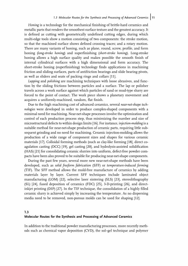
Honing is a technology for the mechanical finishing of brittle-hard ceramics andmetallic parts that renders the smoothest surface texture and the greatest accuracy. Itis defined as cutting with geometrically undefined cutting edges, during whichmulti-edge tools show a motion consisting of two components: the stroke motion,so that the machined surface shows defined crossing traces; and a rotary motion.There are many variants of honing, such as plane, round, screw, profile, and formhoning (long-stroke honing) and superfinishing (short-stroke honing). Long-strokehoning allows a high surface quality and makes possible the smooth finish ofinternal cylindrical surfaces with a high dimensional and form accuracy. Theshort-stroke honing (superfinishing) technology finds applications in machiningfriction and sliding surfaces, parts of antifriction bearings and slide bearing pivots,as well as sliders and seats of packing rings and collars [11].Lapping and polishing are machining techniques with loose abrasives, and func-
tion by the sliding frictions between particles and a surface. The lap or polishertravels across a work surface against which particles of sand or mud-type slurry areforced to the point of contact. The work piece shows a planetary movement andacquires a uniformly-machined, random, flat finish.Due to the high machining cost of advanced ceramics, several near-net-shape tech-
nologies were developed in order to produce complex-shaped components with aminimal need for machining. Near-net-shape processes involve the optimization andcontrol of each production process step, thus minimizing the number and size ofmicrostructural defects to within design limits [16]. For instance, injection-molding is asuitable method for near-net-shape production of ceramic parts, requiring little sub-sequent grinding and no need for machining. Ceramic injection-molding allows theproduction of a wide range of component sizes and shapes for various ceramicmaterials [17]. Colloidal forming methods (such as clay-like forming [18], direct co-agulation casting (DCC) [19], gel casting [20], and hydrolysis-assisted solidification(HAS) [21] for consolidating ceramic slurries into uniform, defect-free powder com-pacts have been also proved to be suitable for producing near-net-shape components.During the past few years, several more new near-net-shape methods have been
developed, such as solid freeform fabrication (SFF) or temperature-induced forming(TIF). The SFF method allows the mold-free manufacture of ceramics by addingmaterials layer by layer. Current SFF techniques include laminated objectmanufacturing (LOM) [22], selective laser sintering (SLS) [23], stereolithography(SL) [24], fused deposition of ceramics (FDC) [25], 3-D-printing [26], and direct-inkjet printing (DIP) [27]. In the TIF technique, the consolidation of a highly filledceramic slurry is achieved simply by increasing the temperature. As no dispersingmedia need to be removed, non-porous molds can be used for shaping [12].
1.3Molecular Routes for the Synthesis and Processing of Advanced Ceramics
In addition to the traditional powder manufacturing processes, more recently meth-ods such as chemical vapor deposition (CVD), the sol–gel technique and polymer
1.3 Molecular Routes for the Synthesis and Processing of Advanced Ceramics j11

pyrolysis have been applied to create high-purity starting materials with definedproperties. Furthermore, these processes can open up new areas of applicationpreviously unrealizable by conventional methods. In all three processes, the ceramicsolid is synthesized on the basis of lower molecular, inorganic or elemental organicprecursors (Figure 1.6).The aim of present research activities in the materials synthesis field is to develop
concepts for the production of novel multifunctional inorganic materials with atailor-made, nanoscaled structure. Industrial demands on future technologies havecreated a need for new material properties which exceed by far those of materialsknown today, and which can only be produced by designing the material structure ata nanoscale. Furthermore, the increasing miniaturization of components calls fornew process technologies which allow the reliable production of materials at andbelow a micrometer scale. In particular, inorganic–organic hybrid materials as wellas amorphous and polycrystalline ceramics are to be used as material classes andproduced by means of crosslinking routes in various states of condensation. Inaccordance with the so-called �bottom-up� approach, specific inorganic moleculesare to be assigned to higher molecular networks and solid-state structures in theform of molecular nanotools by means of condensation and polymerization pro-cesses. This method aims at linking organic components to inorganic structures,thus producing materials inaccessible by thermodynamically controlled chemicalsyntheses. Therefore, experimental studies focus on the development of solidsderived from molecular units via kinetically controlled synthesis processes in theinterface betweenmolecular and solid-state chemistry enabling specific adjustmentsto be made to the solid-state properties. Thus, the ultimate objective of the present-day investigations in this field is to systematically to study the �bottom-up� approachwith regard to the synthesis and exploration of novel materials. In this way it should
Figure 1.6 Molecular materials synthesis can be achieved viachemical vapor deposition (CVD), polymer pyrolysis, or sol–geltechniques. In the latter cases, the so-called �bottom up�approach requires that the molecules must be transformed topolymers before transformation to the desired inorganicmaterial.P, pressure; T, temperature.
12j 1 Modern Trends in Advanced Ceramics

be possible to establish the technological fundamentals for the development of thesenew materials and their potential use. Possible fields of application for materialsproduced at a nanoscale are key technologies of the 21st century such as transportsystems, information technology and energy, as well as environmental systems andmicro- or nano-electromechanical systems. The correlation between the structure ofthe molecular precursors and the nanostructure of the derived materials and theirproperties will provide the focal point for detailed experimental studies.In the following sections, the molecular routes which have great potential for use
in ceramic manufacturing and processing are briefly described.
1.3.1The CVD Process
In the CVD process, lowermolecular, volatile reactants in the gas phase are fed into ahot reaction zone in which a solid reaction product results, which may be collectedeither as a free powder or as a coating on a substrate. The deposition temperaturesfor ceramic products range from 600 to 1500 �C, depending on the reaction system[28,29]. If a plasma or laser is utilized to enhance the chemical reaction rate of theprecursors, the formation of the ceramic product can be effected at temperaturesbelow 500 �C. Some reaction systems and their ceramic products are detailed inTable 1.1. The thermodynamic instability of the gaseous reactants provides thedriving force for the reaction. The total deposition rate depends on the reactionrate, nucleation rate, and diffusion rate. The rate-determining factor at highertemperatures is diffusion, whereas at lower temperatures it is reaction.The CVD process is primarily used for:
. gas-phase infiltration of porous substrates [30]
. coatings and surface modification [24,31]
. production of ceramic whiskers
. high-purity, fine ceramic powders [32]
Figure 1.7 shows a hard, amorphous coating comprised of SiCN derived byplasma-enhanced CVD using a molecular precursor, namely R3Si�N¼C¼N�SiR3
Table 1.1 Reaction systems for chemical vapor deposition (CVD) of ceramic compounds.
Reaction systema Temperature [�C] Ceramic product Process
AlCl3/NH3 800–1200 AlN CVDAlCl3/NH3 400–600 AlN PACVDb
BCl3/NH3 800–1200 BN CVDSi(CH3)4 900–1400 SiC CVDSi(Cl4/NH3 1000–1400 Si3N4 CVDSiCl4/NH3 400–600 Si3N4 PACVDb
aData from Refs. [28] and [29].bPlasma-assisted CVD.
1.3 Molecular Routes for the Synthesis and Processing of Advanced Ceramics j13

with R¼CH3, having all required elements silicon, carbon and nitrogen in themolecular structure [33].In general, the CVD reaction system may be described by Eq. (1)
Aaþ BbÐCc þDd ð1Þ
in which A mole of gas a and B mole of gas b react to C mole of solid phase c(ceramic) and D mole of gaseous reaction product d. The appropriate reactionconditions may be specified as the partial pressures of all the gases and thetemperature.The formation of free ceramic powders in the reactor atmosphere results from
homogeneous nucleation. In contrast, deposition of substrate films or whiskersproceeds by heterogeneous nucleation. Homogeneous nucleation requires a highersupersaturation S of the gas phase [29] which is dependent on the equilibriumconstant K of the reaction system [Eq. (2)] and the partial pressures of the reactantand product gases:
S ¼ ½a�A½b�B½d�D K ð2Þ
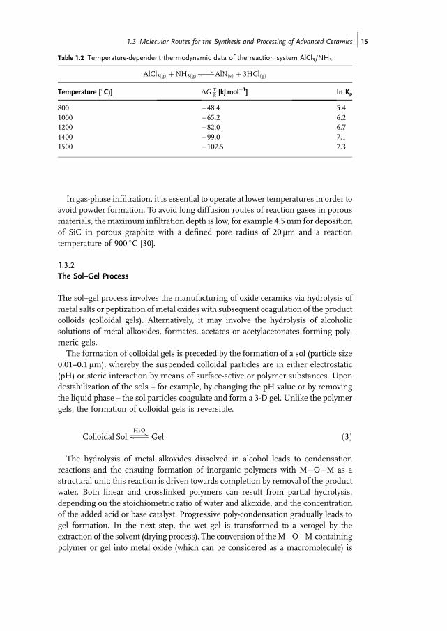
The equilibrium constant itself is strongly temperature-dependent, as exemplifiedby thermodynamic calculations in the system AlCl3/NH3 [32]. The values of K in thetemperature range between 1000 and 1500 �C calculated from the JANAF tables arelisted in Table 1.2 [34]. Due to the temperature dependence of K in accordance withEq. (2), it can be predicted – and confirmed experimentally– that high temperaturesfavor the formation of AlN powders, while low temperatures favor the formation of aAlN substrate film [32].
Figure 1.7 SEM image of a wear track of an amorphous SiCNhard coating on a steel substrate. The coating was produced by aradiofrequency plasma-enhanced chemical vapor depositionprocess (RF PE-CVD) using R3Si�N¼C¼N�SiR3 (R¼CH3) asmolecular single source precursor. The achieved film thickness isin the order of 20mm, and the hardness was determined as beingin the range 21–29GPa. For more details, see Ref. [33].
14j 1 Modern Trends in Advanced Ceramics
In gas-phase infiltration, it is essential to operate at lower temperatures in order toavoid powder formation. To avoid long diffusion routes of reaction gases in porousmaterials, themaximum infiltration depth is low, for example 4.5mm for depositionof SiC in porous graphite with a defined pore radius of 20mm and a reactiontemperature of 900 �C [30].
1.3.2The Sol–Gel Process
The sol–gel process involves the manufacturing of oxide ceramics via hydrolysis ofmetal salts or peptization ofmetal oxides with subsequent coagulation of the productcolloids (colloidal gels). Alternatively, it may involve the hydrolysis of alcoholicsolutions of metal alkoxides, formates, acetates or acetylacetonates forming poly-meric gels.The formation of colloidal gels is preceded by the formation of a sol (particle size
0.01–0.1mm), whereby the suspended colloidal particles are in either electrostatic(pH) or steric interaction by means of surface-active or polymer substances. Upondestabilization of the sols – for example, by changing the pH value or by removingthe liquid phase – the sol particles coagulate and form a 3-D gel. Unlike the polymergels, the formation of colloidal gels is reversible.
Colloidal SolÐH2OGel ð3Þ
The hydrolysis of metal alkoxides dissolved in alcohol leads to condensationreactions and the ensuing formation of inorganic polymers with M�O�M as astructural unit; this reaction is driven towards completion by removal of the productwater. Both linear and crosslinked polymers can result from partial hydrolysis,depending on the stoichiometric ratio of water and alkoxide, and the concentrationof the added acid or base catalyst. Progressive poly-condensation gradually leads togel formation. In the next step, the wet gel is transformed to a xerogel by theextraction of the solvent (drying process). The conversion of theM�O�M-containingpolymer or gel into metal oxide (which can be considered as a macromolecule) is
Table 1.2 Temperature-dependent thermodynamic data of the reaction system AlCl3/NH3.
AlCl3ðgÞ þNH3ðgÞÐAlNðsÞ þ 3HClðgÞ
Temperature [�C)] DGTR [kJmol�1] In Kp
800 �48.4 5.41000 �65.2 6.21200 �82.0 6.71400 �99.0 7.11500 �107.5 7.3
1.3 Molecular Routes for the Synthesis and Processing of Advanced Ceramics j15

accomplished via heat treatment in several calcination steps entailing the followingreactions subject to the temperature:
. 100–200 �C: separation of adsorbed solvent particles (water,alcohol)
. 200–600 �C: decomposition of organic residues and hydroxide,nitrate, sulfate, etc.
. 100–700 �C: inter- and intramolecular separation of water andalcohol forming the corresponding metal oxide.
As demonstrated in detailed investigations on the hydrolysis of tetraethoxy silane,the complete hydrolysis of alkoxides provides sol particles which aggregate to form acolloidal gel according to the pH value or dilution [35]. Some examples of oxidematerials produced by hydrolysis of metal alkoxides via this process are listed inTable 1.3.The drying process plays a decisive role in the production of defect-free gels – that
is, dense, crack-fee monolithics. During drying, considerable capillary forces comeinto play, and such forces increase with decreasing capillary radius according to theLaplace equation [36,37]:
DP ¼ 2gcosQ=rp ð4Þ
Here rp is the capillary radius,g is the surface energy of the liquid, and Y is thecontact angle at the gel–liquid– air interface. The capillaries may collapse upon crackformation, as discussed in detail by Scherer [37] or Defay [36].In order to avoid crack formation, the gel must be dried at an extremely slow rate
under controlled vapor pressure of the solvent. As the drying rate is inverselyproportional to the sample thickness, the crack-free drying process may take severalweeks. After overcoming these initial difficulties, it was nevertheless possible tocreate ceramic products with larger dimensions directly from alkoxides. Thus, high-purity glass panes for optical applications could be obtained [45].An understanding of the hydrolysis kinetics of the individual metal compounds
plays a decisive role in the hydrolysis of alkoxide mixtures for the production ofmultiphase ceramics. Double alkoxides such as Mg[Al(OR)4]2 with R¼Alkyl [44] are
Table 1.3 Metal alkoxides for the production of oxidic ceramics.
Metal alkoxide Ceramic
Ba(OEt)2 BaO [38]Y(OPri)3 Y2O3 [39]Al(OEt)3 Al2O3 [40]Si(OEt)4 SiO2 [41]Ti(OEt)4 TiO2 [42]Zr(OEt)4 ZrO2 [43]Mg[Al(OEt)4]2 MgAl2O4 [44]
16j 1 Modern Trends in Advanced Ceramics

present in the solution as molecular species, and therefore exhibit uniform reactionkinetics in the hydrolysis process:
Mg½AlðORÞ4�2 �������!H2O Mg½AlðOHÞ4�2 �������!T � 500�CMgAl2O4 ð5Þ
Therefore, starting from Mg[Al(OR)4]2 it is possible to manufacture a phase-purespinel, for example a spinel membrane, via the sol–gel process. The membrane isapplied to a microporous substrate made of a-Al2O3 in the form of a crack-free filmapproximately 1mm thick with an average pore radius of approximately 5 nm. Uponcalcination at 1200 �C, the deposited spinel particles exhibit crystal sizes smallerthan 50 nm [46].The Mg–Al double alkoxide was suggested by Greil et al. for the homogenous
coating of commercial Si3N4 powders to provide spinel sintering additive [47]. Othermetal alkoxides, such as Ti(OEt)4, Si(OEt)4 or Ba(OEt)2, have also been used to coatceramic powders in order to ensure a uniform distribution of the sintering additives,directly influencing grain growth during the densification process, or to form crys-talline secondary phases [48,49].The sol–gel process may also be used to create monodisperse, submicrometer
powder particles which could aid sintering because of a better packing density [50].Thus, according to Barringer and Bowen, monodisperse Al2O3 can be sintered at1250 �C instead of 1750 �C, as is common in the densification of conventional Al2O3
powders [51]. However, since colloidal crystals still contain defects such as grainboundaries over a longer length scale, there is no significant advantage of usingmonodisperse powders in practical applications.The sol–gel process is also applied for the production of oxide glass fibers and
ceramic fibers [52,53], as well as for surface modification. The sol–gel coating ofglass has been used in industry since the early 1970s [44]. Depending on thecomposition of the glass layer, it is possible to manufacture reflective or anti-reflec-tive films [54], passive, and doped coatings (for microelectronics). Furthermore, it isalso possible to produce films which, due to their low thermal expansion comparedwith the substrate, generate compression stress, thereby drastically increasing themechanical strength of the glass [55]. As reported by Schubert [56,57], metal ceramicnanocomposites can be created by metal–ligand complexation bonded to silicon inthe glass structure.A further application of the sol–gel process is the production of organically
modified silicates, the so-called ormosils. Ormosils (e.g., poly(methyl)siloxane) in-clude non-hydrolyzable organic groups, and can be classified as inorganic–organichybridmaterials [48,51]. Their mechanical properties lie between those of pure glassand plastics.
CH3SiðORÞ3 �������!H2O ½CH3SiO1:5�n þ ROH; R ¼ Alkyl ð6Þ
In particular, ormosils are used to coat contact lenses, as scratch-resistant surfacescan be created [58].
1.3 Molecular Routes for the Synthesis and Processing of Advanced Ceramics j17

A non-aqueous sol–gel process was developed for the first time in 1997 whichallowed the synthesis of nitrides and carbides by this method. A poly(methylsilyl-carbodiimide)-gel formation is shown in Figure 1.8 for the reaction of CH3SiCl3 withR3Si�N¼C¼N�SiR3 (R¼CH3) according to reaction Eq. (7) [59]:
nCH3SiCl3 þ 1:5n R3Si�N ¼ C ¼ N�SiR3 ðR ¼ CH3Þ!½CH3SiðNCNÞ1:5�n þ nðCH3Þ3SiCl
ð7Þ
A variety of other chlorosilanes as well as chlorine-substituted boron derivates(e.g. BCl3) or B-trichloroborazene can be reacted with R3Si�N¼C¼N�SiR3 to formnon-oxide gels [60]. In a final step, the gels are transformed to glasses and ceramicsby a thermal treatment up to 1000–1300 �C [59].
1.3.3Polymer-Derived Ceramics (PDCs)
The production of non-oxide ceramics starting from polymeric precursors wasreported for the first time during the early 1960s [61], although the first synthesisof a SiC material from polycarbosilane precursor dated back to the reports by Fritz[62] in 1956 and Yajima in 1957 [63]. Some years later, the first practical applicationwas reported, namely the manufacture of small-diameter Si3N4/SiC fibers frompolyorganosilicon precursors for high-temperature use [64]. The Yajima process forthe synthesis of SiC materials by thermolysis of polycarbosilanes was subsequentlyreported during the late 1970s [65].
Figure 1.8 Non-aqueous sol–gel process developed for thesynthesis of amorphous SiCN-gels. The gel is produced by thereaction of organochlorosilanes such as CH3SiCl3, withR3Si�N¼C¼N�SiR3 (R¼CH3) in the presence of pyridine ascatalyst (see Ref. [59]).
18j 1 Modern Trends in Advanced Ceramics

Silicon-based polymers have proven to be promising precursors for the produc-tion of advanced ceramic components such as fibers, coatings, infiltrated porousmedia, or complex-shaped bulk parts. In recent years, many examples of polysilanes,polycarbosilanes, polysilazanes and polysiloxanes as precursors for ceramics havebeen reported [66].Poly(organo)siloxanes are versatile materials, showing excellent chemical and
physical properties. Examples of poly(organo)siloxanes are [R2Si�O�]n or [RSi(O)1.5]n, with R¼H, alkyl, aryl, etc.. These have been used extensively for preparingSiCO ceramicmaterials via pyrolysis in inert or reactive atmospheres [67]. They haveunique thermomechanical properties owing to the combination of pronouncedelasticity at unusually low temperatures, and high thermal and thermo-oxidativestability at elevated temperatures. At the macroscopic level, the low-temperatureelasticity of polysiloxanes is primarily manifest in some of the lowest glass transitiontemperatures (Tg) known for polymers, low crystalline melting points (Tm), unusuallyrapid crystallization, specific liquid crystalline (LC) behavior, and small viscosity–temperature coefficients [68]. Essentially, these properties are determined directly bypolymer segmental chain mobilities which are all governed by the inherent chainflexibility (Si�O�Si with angles from 140� to 180�) and relatively weak intra- andintermolecular interactions.Similar to the low-temperature properties, the high-temperature stability and the
degradation of polysiloxanes are also determined directly by the specific interplay oftheir structural building blocks – that is, the inherent strength of the siloxanebond andthepronouncedflexibility of Si�Osegments and thewholemolecule. Thepartial ionicand double bond character of the Si�O bond in siloxanes leads to its exceptionalhomolytic strength, since both effects increase the binding force between the partici-pating silicon and oxygen atoms. The reason for this was the unique additional dp�ppbond between Si and O resulting in an Si�O bond dissociation energy of about108 kcalmol�1, which is considerably higher than, for example, those of C�C bonds(82.6 kcalmol�1), C�O bonds (85.2 kcalmol�1), or even Carom�C bonds (97.6 kcalmol�1) [68]. Consequently, the Si�O bond can withstand exposure to higher tem-peratures than the bonds normally found in organic polymers. Thus, polysiloxanes asa class exhibit higher thermal stabilities than their C�C counterparts.Silicon oxycarbide glasses can be produced only by the pyrolysis of polysiloxanes.
These amorphous materials are typically black-colored due to the presence of a freecarbon phase. Several studies conducted during the past few years have focused on theseparation of free carbon and the microstructural development of silicon oxycarbideceramics [69]. Furthermore, the modification of SiCO materials by boron and alumi-numhas attracted recent interest due to its strong influence on the thermomechanicalproperties and microstructure development of the silicon oxycarbide ceramics. Forinstance, the presence of boron in SiCO glasses inhibits the separation of free carbon,thus providinghigher electrical resistivity. It has been shownvia transmission electronmicroscopy (TEM) studies that the presence of boron induced a modified behavior inthe microstructure development, in that an enhancement of finely dispersed b-SiCnanocrystallites embedded in a high-temperature stable amorphous SiBCO phasewithout the formation of a-cristobalite were observed for SiBCO ceramics [70]. Due
1.3 Molecular Routes for the Synthesis and Processing of Advanced Ceramics j19

to its high temperature resistance and stable electrical properties, SiBCO is a candidatematerial for ceramic heaters.Poly(organo)silazanes which contain �Si�NH� structural units are isoelectronic
to polysiloxanes, are precursors for the production of silicon nitride and siliconcarbonitride (SixCyNz) ceramics through high-temperature pyrolyses [71]. Althoughthe bonding energy of the Si�O bond is higher than that of Si�N (432 and 316 kJmol�1, respectively), polysilazanes have been shown to be more thermally stablethan polysiloxanes. Solid-state 29Si NMR-studies have shown that polysilazane-de-rived Si�C�N materials are single-phase amorphous silicon carbonitride-contain-ing SiCxNy (xþ y¼ 4) units [72]. The insertion of boron in polysilazanes induces adramatic enhancement of the thermal stability, and also retards crystallization up to1800 �C. Si(B)CN ceramics can be heated to 2000 �C without degradation due to anetwork rearrangement which allows the amorphous Si(B)CN phase to encapsulatea-Si3N4 crystals, hindering the latter compound�s thermal decomposition [73].Polysilylcarbodiimides containing structural units of the form �Si�N¼C¼N�
were first synthesized by Pump and Rochow via metathesis reactions of dichlor-osilanes and bis(silyl)cyanamide [74]. Some three decades later, it was shown thatpolysilylcarbodiimides of the form [R2Si�N¼C¼N�]n, [RSi(N¼C¼N)1.5]n, and [Si(N¼C¼N)2]n with R¼H, alkyl or aryl, can serve as precursors for Si�C�N ceramics.Starting from polysilylcarbodiimide derivatives, the first two crystalline phases in theSi�C�N system were identified as SiC2N4 and Si2CN4 [75]. Furthermore, it wasfound that the synthesis of polysilylcarbodiimides starting from chlorosilanes andbis(trimethylsilyl)carbodiimide, R3Si�N¼C¼N�SiR3 (R¼CH3), in the presence ofcatalytic amounts of pyridine, occurs similarly to the aqueous reactions of alkox-ysilanes by means of the sol–gel process. Thus, in the non-oxide sol–gel process, bis(trimethylsilyl)carbodiimide adopts the role of H2O, leading to Si�C�N-based gelswhich can be calcinated or/and pyrolyzed to Si�C�N amorphous ceramics [76].Polysilanes and polycarbosilanes are classes of materials which have been subjected
to a large number of investigations due to their intriguing opto-electronic propertiesthat originate from their typical s-conjugation [77]. For example, peralkyloligosi-lanes may find potential applications in photoconducting and charge-transportingmaterials [78]. A major factor in the interest is their use as precursors for siliconcarbidematerials, especially in the Yajima process for continuous SiC ceramic fibers.In summary, silicon-containing pre-ceramic polymers provide the unique possi-
bility for the synthesis of new ceramic systems, not only Si�C�O and Si�C�N butalso Si�E�C�O (E¼B, Al, Ti) and Si�E�C�N (E¼B, Ti), which cannot be synthe-sized by means of the �classical� powder method. Since tailored properties of thefinal ceramic material can be achieved by chemical modification of the polymericprecursor, the PDC route offers an exceptional opportunity to synthesize novelmulti-component materials with outstanding properties. These include extraordinaryhigh-temperature and corrosion resistance, oxidation stability, and promising electric,magnetic and optoelectronic properties of interest for advanced ceramic applications[66]. Some examples of silicon-based polymers consolidated by warm pressing, andthe ceramic products obtained by subsequent pyrolysis of the formed polymers, areshown in Figure 1.9.
20j 1 Modern Trends in Advanced Ceramics

1.4Methods for Characterization of Advanced Ceramic Materials
The characterization methods for advanced ceramics can be divided into optical, X-ray and electron spectroscopy techniques, resonance characterization methods,diffraction techniques, electron optical methods, and surface characterization meth-ods. In addition, there are a variety of characterization methods which relate to thethermal and mechanical properties of ceramic materials. Some of these techniquesare briefly described in the following sections.Atomic emission spectroscopy (AES or OES) uses quantitative measurement of the
optical emission fromexcited atoms in order to determine analyte concentrations. Theanalyte atoms are vaporized and atomized by a flame, discharge, or plasma. This high-temperature atomization process provides sufficient energy to promote the atoms intohigh energy levels. The atoms then decay back to lower levels by emitting light. As thetransitions are processes between distinct atomic energy levels, the emission lines inthe spectra arenarrow.Themajor advantageof this technique (compared, for example,
Figure 1.9 Optical micrographs of warm-pressed, silicon-based polymersand ceramic products derived therefromby pyrolysis of the polymer at 1100 �Cin Ar. (a) Crosslinked and warm-pressedpolysilazane Ceraset�. (b) Amorphous SiCN
ceramic obtained by pyrolysis of sample shownin (a). (c) Crosslinked and warm-pressedpolysiloxane (Wacker, MK-polymer). (d)Amorphous SiCO ceramic obtained by pyrol-ysis of sample shown in (c).
1.4 Methods for Characterization of Advanced Ceramic Materials j21
with atomic absorption spectroscopy, AAS), is that all the atoms in the sample areexcited simultaneously, and thus can all be detected at the same time. Various AEStechniques are available, depending on the atomization source: direct current plasma(DCP); inductively coupled plasma (ICP); laser-induced breakdown excitation sources(LIBS); microwave-induced plasma (MIP); and spark and arc emission sources. Thecombination of electrothermal vaporization (EVT) with inductively coupled plasmaatomic emission spectroscopy (ICP-AES)was shown to be a promisingmethod for theanalysis of ceramic powders [79]. Since carbide-forming elements in powderedceramicmaterials are difficult to vaporize, several studieswere conducted on chemicalmodifiers. Substances such as KF, (C2F4)n, Na2B4O7, BaCO3, Ba(NO3)2, BaO, AgCl,CoF2 and Pb(BO2)2, as well as combinations thereof, can be used to achieve totalevaporation of elements from any type of powdered sample [79].X-Ray photoelectron spectroscopy (XPS, ESCA) is a surface quantitative spectroscopic
technique that measures the chemical formula, chemical state, and electronic state ofthe elements that exist within a material. This technique uses monoenergetic softX-rays which cause electrons to be ejected. Identification of the elements in thesample can bemade directly from the kinetic energies of these ejected photoelectrons.Furthermore, the relative concentrations of elements can be determined from thephotoelectron intensities. Other surface electron spectroscopy techniques includeAuger electron spectroscopy (AES) and electron energy loss spectroscopy (EELS).In order to study the chemical composition and chemical bonding situation in
ceramic materials, resonance methods such as ESR, NMR and Mössbauer spectros-copy are used. For instance, solid-state NMR spectroscopy can be used for the micro-structure analysis of silicon-containing amorphous polymer-derived ceramics(PDCs). By using 29Si MAS NMR studies, it was found that polysilazane-derivedSi�C�N ceramic materials showed only one amorphous Si�C�N phase, whereaspolysilylcarbodiimide-derived PDCs consisted of amorphous Si3N4 nanodomainsinterconnected by amorphous carbon (for details, see Figure 1.10) [80].The availability of tunable X-ray sources of a specific energy from synchrotrons
allows X-ray spectroscopy to be used in a resonance mode that probes the excitation ofcore electrons of selected atoms instead of all the elements in the sample. As itreflects the electronic structure of unoccupied states of the selected element, thismethod is sensitive to the local environment of the selected atom. X-ray absorptionspectra (XAS) show sharp absorption edges, followed by a decay curve which showssome fine structure called X-ray absorption fine structure (XAFS) [81]. The first 30 to50 eV of XAFS correspond to X-ray absorption near edge structures (XANES),whereas the remainder of the spectrum is referred to as extended XAFS (EXAFS).Both XANES and EXAFS are sensitive to the local environment of the atoms andprovide complementary information. Whereas XANES is sensitive to the chemicalenvironment of the specific element, such as chemical bonding, charge state, mag-netic state, EXAFS provides quantitative information about the local coordination ofthe atom such as coordination number and bond length. With reference to a stan-dard and in combination with theoretical tools, XANES and EXAFS can serve as apowerful tool when analyzing small amounts of elements in various samples, suchas ultra-thin films and ultra-dilute dopants [81].
22j 1 Modern Trends in Advanced Ceramics

The electron energy loss near edge structure (ELNES) corresponds to the low-energy domain of electron energy loss spectrum (EELS) [82]. Whenmeasured in thetransmission geometry, ELNES furnishes information which is almost identical tothat provided by XANES. The ELNES/XANES technique has found applications in
Figure 1.10 Solid-state NMR study of amor-phous materials in the SiCN system. (a) 29Si-MAS-NMR spectra of polysilazane-derivedamorphous SiCN ceramic annealed at the giventemperatures. (b) 29Si-MAS-NMR spectra ofpoly(silylcarbodiimide)-derived amorphousSiCN ceramic annealed at 1400 and 1500�C.While in (a) two chemical shift values are clearlydeveloped at �18 ppm and �48.5 ppm indi-
cating the presence of SiC4 and SiN4 tetrahedra,the spectra of the poly(silylcarbodiimide)-derived SiCN ceramic exhibit only the resonancecorresponding to SiN4 moieties. The presenceof the small shoulders at �34 and �21 ppm inthe spectrum of the material annealed at1500 �C indicates that the formation of mixedSiCxN4-x tetrahedra (x = 1�3) starts at thistemperature.
1.4 Methods for Characterization of Advanced Ceramic Materials j23

the identification of polymorphs (GaN, AlN, InN, and ZnO) [83], the characterizationof superficial and interfacial thin films [84], the identification of ultra-dilute dopantsor impurities [85], solving the atomic structure of solid solutions, or in describingdiluted magnetic semiconductors, such as ZnO:Mn polycrystalline materials [86].In order to extract statistically representative information on the microstructure of
advanced ceramics, such as void volume fraction, void size distribution, internalsurface areas, pore morphologies, small-angle scattering (SAS) has been shown to bea good characterization method that complements other techniques such as X-raymicrotomography or electron microscopy [87]. The quantitative parameters obtainedfrom small-angle X-ray scattering (SAXS) or small-angle neutron scattering (SANS)complement the visual information obtained by scanning electronmicroscopy (SEM)and TEM or X-ray microtomography (XMT), the phase composition information asobtained by X-ray diffraction (XRD) and neutron diffraction (ND), and informationobtained from other methods, from NMR to light scattering [87]. In particular, SASmethods (SAXS and SANS) provide information over macroscopic sample volumes,whereas electronmicroscopy only providesmore local information for a small volume.Thus, SAS methods have found applications in the characterization of structural,electronic ceramics and glasses, in describing sintering, cavitation and damage pro-cesses, in quantifying microstructures with high interface densities, as well as indiagnostic studies of nanostructured, fractal materials and suspensions [87].Transmission electron microscopy is a versatile electron optical technique to charac-
terize microstructures, and has been used intensively for advanced ceramics inorder to understand their properties, including grain boundary and interface phe-nomena [88]. For example, the TEM image shown in Figure 1.11 reveals the typicalmicrostructure of a Si3N4/SiC micro/nano-composite obtained by liquid-phase sin-tering of an amorphous SiCN powder. The image shows clearly that nano-sized SiCcrystallites are embedded within micron-sized silicon nitride crystals, though some
Figure 1.11 Transmission electron microscopy image of a Si3N4/SiC micro/nano composite obtained by liquid-phase sintering ofamorphous polysilazane-derived SiCN powder. The arrows in-dicate nanosized SiC crystallites. (Illustration courtesy R. Riedel.)
24j 1 Modern Trends in Advanced Ceramics

SiC is also found in the intergranular region. According to the design concept ofstructural ceramics developed by Niihara, this type of microstructure is denoted asan intra/inter-type nanocomposite [89]. In extensive studies, Niihara found thatnanocomposites exhibited significantly enhanced mechanical properties.The resolution of conventional high-resolution electron microscopy (HREM) is
0.17 to 0.20 nm at 200 to 300 kV, thus making the discrimination of atoms which arelocated closer than this distance impossible. Better resolutions of approximately0.1 nm can be achieved with high-voltage atomic resolution electron microscopy(HVAREM). Using this technique, it is possible to discriminate light atoms, forexample Ga and N, in GaN thin films [90]. A combination of HREM techniques,using methods such as nano-electron diffraction, energy dispersive X-ray spectros-copy (EDX) and electron holography, makes it possible to clarify atomic rearrange-ment, composition and electronic state structure of the nano-regions in advancedceramics [91].Although ceramics are hard, wear-resistant materials that retain a good degree of
their mechanical properties even at high temperatures, they are very brittle and areunable to deform plastically undermechanical stress. For example, while hardmetalsmay have a fracture toughness of up to 20MPam�1/2, most advanced ceramics havetoughness below 10MPam�1/2 [92] The failure of ceramic materials is dominated byfracture originating from sources of stress concentration – that is, their mechanicalperformances are dominated by the presence of processing defects (such as porosity,impurities, and microcracking) as much as by the microstructure [93].There are several aspects of the microstructure which should be taken into
account when describing the mechanical features of ceramic materials. The first isthe physical nature of the features, such as the composition and crystal structure ofthe solid phases, and the presence of pores, microcracks, and impurity phases. Thesecond aspect involves the microstructural scale of the features, such as their size,size distribution, volume fraction, and microstructural homogeneity. The thirdaspect is the orientation of microstructural features (e.g., morphological and crys-tallographic anisotropy) [93]. Thus, the challenge is to design materials with a phaseand microstructure that delivers both high hardness and fracture toughness.The fracture toughness in ceramics can be improved by various extrinsic shielding
mechanisms, such as in-situ toughening (growth of platelets or whiskers within themicrostructure), transformation toughening (transformation of tetragonal zirconiagrains into the lower densitymonoclinic phase at the crack tip, thus generating crackclosure forces), crack deflection, crack bridging (filament or fiber toughening), ormicrocrack toughening [94].Hardness is defined as resistance to penetration [95], thus relating to a response of
the surface to a mechanical load. Therefore, hardness is not necessarily a bulkproperty, and should be differentiated from strength [93]. There are typically twostandard methods for measuring the hardness of ceramics, namely the Knoop andVickers techniques. These involve the application of a load via a geometricallydefined indenter, such as a steel ball (as in the Rockwell technique), a diamondsquare pyramid (Vickers), or an elongated diamond pyramid (Knoop). Althoughthere is a well-known dependency of hardness on load, a full characterization by
1.4 Methods for Characterization of Advanced Ceramic Materials j25

hardness–load relationships is rather uncommon for ceramics (Figure 1.12). Fur-thermore, there is no relationship for converting different hardness test values (suchas Knoop to Vickers hardness), thus making the hardness comparison of differentceramic materials difficult. Studies on the Vickers hardness of several brittle cera-mics show hardness–load curves which exhibit a distinct transition to a plateau ofconstant hardness level; this involves a relationship between hardness (H), Young�smodulus (E), and fracture toughness (KIC). Using these parameters, a �brittlenessindex� B was proposed that is derived from deformation and fracture energy ratios(B�HE/KIC
2) and was claimed to have a potential predictive value in ceramic designapplications [92].Besides toughness and hardness, there are several mechanical properties of
ceramic materials which are relevant to their applications, including wear resistance,hot hardness, creep resistance, tribochemical stability, and thermal expansion coefficient.Due to the thermal activation of additional deformationmechanisms (cross-slip of
dislocations, creep via grain boundary and lattice diffusion, or viscous flow) thehardness decreases when materials are subjected to high temperatures. Symmetryof the crystal structure has dramatic effects on the hot hardness of the materials: forexample, cubic boron nitride shows at ca. 600 �C only 50% of its original hardness,while the hardness of diamond decreases remarkably at about 1100 �C. Materialswith less-symmetric crystal structures have fewer easy slip directions for thermallyactivated dislocation, thus featuring higher hot hardness values (e.g., B4C, which isthe hardest material known at temperatures around 1000 �C) [96].The thermal expansion coefficient is a critical thermomechanical property of ad-
vanced ceramic materials, when either a composite, a material joint or a coating on asubstrate is exposed to large changes in temperature. Thus, a misfit between thethermal expansion coefficients of the materials may cause cracking and delamina-tion. For this reason, materials with low expansion coefficients are usually preferred,typically for cutting applications.
Figure 1.12 Hardness versus load relationship of a SiC-basedceramic, showing the strong dependence of the measuredhardness of the applied load expressing the difficulties todetermine a reliable hardness value [135].
26j 1 Modern Trends in Advanced Ceramics

1.5Applications of Advanced Ceramics
During the past few decades, advanced ceramics have been used for industrialapplications due to their uniquemechanical, thermal, chemical, electrical, magnetic,optoelectronic, superconducting and gas-sensing properties. As such, ceramics havebecome important for advanced technologies such as energy transformation, storageand supply, information technology, transportation systems,medical technology andmanufacture technology. Several examples are given below.When used as cutting and slitting tools, advanced ceramics may show many ad-
vantages over metal and conventional tungsten carbide tools, since they are hard,inert, non-metallic, and non-magnetic, retain their properties at high temperatures,and have longer lifetimes. Today, advanced ceramics find widespread use in ma-chining and finishing applications. Ceramics used for cutting tools include alumi-na–silicon carbide whisker composites, silicon nitride, titanium carbide/titaniumnitride materials (cermets), SiAlONs, alumina–titanium carbide composites, poly-crystalline diamond and cubic boron nitride [97].Advanced ceramics are also very attractive for electronic applications as they can
operate at high power and high frequencies, at high temperatures, and in harshenvironments, and also combine properties such as electrical insulation and mag-netism which is not possible for metals. Using chemically synthesized powders,materials such as oxides, nitrides, carbides, and borides have been fabricated withtailored microstructures and properties (including band gap, electron or hole chargecarrier mobility) for electronic applications.A recent example of newly synthesized materials explored for semiconductor and
electro-optic applications is binary nitrides with spinel (Si3N4, Ge3N4) and thoriumphosphate (Zr3N4, Hf3N4) structures. Besides high hardness, the novel nitridepolymorphs of Si3N4 and Ge3N4 possess a direct band gap between 3.0 and 4 eV,which is comparable to the UV/blue light-emitting diode materials based on Al, Gaand In nitride [98,99]. The first such silicon nitride (cubic g-Si3N4) was synthesizedunder a high pressure [100]. Other cubic spinel nitrides since studied [101,102]showed that manyM3N4 (M¼C, Si, Ge, Sn, Ti, Zr) and c-AB2N4 (A¼C, Si, Ge, Sn, Ti,Zr, Hf; B¼C, Si, Ge, Sn, Ti, Zr, Hf ) compounds may also have interesting properties.Another example of emerging ceramic semiconductors is that of silicon carbide.
This material has excellent mechanical properties, oxidation resistance and corro-sion resistance at high temperatures, and a band-gap (3.2 eV) which is three time aswide as that of silicon. This allows the application of SiC in semiconductor devicesused in power electronics. A high electron velocity and a low intrinsic carrierconcentration are other interesting properties of SiC. Various bulk growth methodsfor SiC single crystals have been developed during the past few years to facilitatethese new applications [103].Among insulators, one area where very rapid growth has been witnessed for
ceramics is that ofmicrowave applications. Temperature-stable, medium-permittivitydielectric ceramics have been used for decades as resonators in filters for microwavecommunication due to their very low dielectric loss (high-quality factor) and their
1.5 Applications of Advanced Ceramics j27

high permittivity. Thus, ceramic materials with simple and complex perovskitestructures such as (Mg,Ca)TiO3, ZrTiO4, BaTi4O9, BaZn1/3Ta2/3O3 (BZT), Ca-TiO3-NdAlO3 (CTNA), ZrTiO4-ZnNb2O6 (ZTZN), Ba(Co,Zn)1/3Nb2/3O3 (BCZN) areused for base station resonators, whilst Ba4Nd9.33Ti18O54-based compounds findapplication as receivers in digital televisions [104].Piezoceramics are materials which couple electrical and mechanical stimuli/re-
sponses. For example, when a mechanical force is applied, an electrical responsearises which, in terms of voltage or charge, is proportional to the magnitude of theapplied stress. Conversely, when an electric field is applied, a mechanical stress ordeformation/shape change develops. Ceramics are widely used for electromechani-cal sensors and actuators. Some examples of piezo materials are crystalline quartz,barium titanate, vanadium niobate and lead zirconate titanate (PZT). Some of thesepiezomaterials, such as quartz, are single crystals which are not polarized in thestress-free state and whose piezoelectricity depends only on the crystal orientation.Other piezoelectrics, such as PZT, contain domains of spontaneous polarizations ofdifferent orientations [105]. Since the domains in the as-prepared materials arerandomly oriented, a poling process is required in order to achieve domain align-ment that gives rise to net piezoelectricity. This process is usually performed under ahigh electric field (ca. 10 kVcm�1) at slightly elevated temperatures (ca. 100 �C) for ashort time.During recent years, polymer-derived ceramics (PDCs) have been demonstrated
as being new materials suitable for micro electromechanical system (MEMS) applica-tions, especially at relatively high temperatures. MEMS is a device that often involvestransduction processes which couple mechanical, electrical, thermal, magnetic,radiant, and chemical processes [106]. For instance, SiCO ceramics have been usedin the preparation of MEMS by using mixtures of polysiloxane polymers with avariety of active (Ti, TiH2, Al) or passive (SiC, Al2O3, TiB2) fillers. Under micromolding, these polymers melt, are then solidified by chemical or thermal cross-linking, and the shaped green body is subsequently pyrolyzed to the final MEMScomponent. In this way, SiCO micro gear components [107,108] and a SiCON [109]micro igniter (Figure 1.13) have recently been developed using the polymer-to-ceramic transformation process.Advanced ceramics are also increasingly used as materials for prostheses, such as
orthopedic and dental implants, due to their good combination of stability, biocompati-bility, strength, and wear resistance [110]. For example, leucite-reinforced glass cera-mics have been used for dental implants (crowns), showing fracture strengths of95MPa [111] compared to porcelains that have fracture strength values of ca. 70MPa.Zirconia (typically a solid solution with 3mol.% Y2O3 to stabilize the tetragonal form)is also used commercially for this purpose. Tetragonal zirconia and aluminahave beenused as femoral heads in total hip replacements; zirconia (in the tetragonal form) hasbetter strength and toughness, but aluminahas abetter thermal conductivity. Recently,alumina–zirconia nanocomposites were also explored for joint prostheses. The ma-terials were synthesized by a new colloidal processing route which involves a stablesuspension of high-purity alumina in diluted solutions of zirconium alkoxide. Due tothe small size of zirconia nanograins and the narrow grain-size distribution thereof,
28j 1 Modern Trends in Advanced Ceramics

larger amounts of tetragonal zirconia could be retained in the material, thus contrib-uting to improved fracture toughness (5.9MPam�1/2 for 10 vol.% ZrO2). These na-nocomposites can function at loads which are two-fold higher than the monoliths(ZrO2 or Al2O3), without delayed fracture. Additionally, they show similar hardnessvalues to alumina and are not susceptible to the hydrothermal instability observed incase of zirconia bioceramics [112].Solid oxide fuel cells (SOFCs) utilize the rapid ionic conductivity of either oxygen or
proton to allow solid-state charge transport across an oxide (electrolyte) membranethat separates oxidation and reduction reactions on two sides, consuming oxygenand fuel (H2 or hydrocarbons). SOFCs offer the potential for efficient power gener-ation in distributed power systems and transport systems, resulting in lower CO2
emission and reduced pollution from combustion products such as NOx and SOx.SOFCs have some advantages over other types of fuel cell, for example their highoperation temperatures allow the flexibility in the type of fuel that can be used [113].Standard SOFCs operate at temperatures of about 900–1000 �C, and use yttria-stabilized zirconia (YSZ, in the cubic form) as electrolyte. These high temperatures,however, generate considerable constraints on the materials that can be used forinterconnections and balance of plant (e.g., LaCrO3 degrades during long-termoperation). Thus, some recent developments focus on new electrolytes (such asCe(Gd)O2�x or La(Sr)GaO3) that can maintain a sufficiently high ionic conductivityat lower operating temperatures of about 800 �C. A lower operating temperaturemayalso allow the application of other cell concepts which, along with improved fabri-cation processes, may have a significant potential for reducing the fabrication costsof SOFCs [114].Chemical sensing is another application where the ionic or electronic conductivity
of oxide ceramics is utilized. As the world becomes more environmentally andsecurity conscious, chemical sensors are increasingly used in a wide range ofindustrial and consumer applications, such as steelmaking, metal casting, power
Figure 1.13 A micro igniter based on SiCON and produced froma pre-ceramic polymer. (Source: Rishi Raj, University of Coloradoat Boulder.)
1.5 Applications of Advanced Ceramics j29
plants, airplanes, automobiles, and public safety. Many of these applications demandrugged and reliable sensors capable of operation in harsh environments. Chemicalsensors detect the presence of various gases (CO, NOx, O2, CO2, hydrocarbons, andvolatile organic compounds) for emission control and air quality monitoring, as wellas early warning of smoke, fire, and hazardous chemicals in public places and masstransportation systems [115]. One oxygen sensor, which is used in every vehicle foremission and combustion control, utilizes the same above-mentioned YSZ forSOFCs. In this application, a galvanic signal develops across the YSZ electrolyteto correspond to the partial pressure of oxygen in the exhaust gas. Many gas sensorsuse semiconductor metal oxide-based ceramic materials. These remain stable in airat high temperatures while reacting with gases (some of them are chemically ag-gressive) at their surfaces, without undergoing irreversible chemical reactions, aswould other semiconductors (e.g., Si) [116]. These sensors may be broadly classifieddepending on how they utilize the various interaction mechanisms at the sensorsurface: bulk conduction-based sensors (TiO2, BaTiO3, CeO2, Nb2O5), metal/oxidejunction controlled sensors (Pd/SnO2, Pt/TiO2), and surface-layer conductive sen-sors. For example, SnO2-based bulk-type sensors integrated with a direct or anindirect heating coil (Ir–Pd or Cr alloy wire) operating at temperatures of 300–450 �Care widely used for toxic and inflammable gas leak detectors [116]. In addition to YSZand SnO2, perovskite-type oxides (ABO3) are well represented in sensor applicationsdue to their ability to exhibit a wide range of ionic and electronic conductionbehaviors. For example, LnFeO3-based (Ln¼La, Sm) sensors have shown goodsensitivity to CO and NO2 [117], and SmFe1�xCoxO3-based sensors have showngood response and recovery behavior to O3 and NO2 [117]. Another ceramic ofinterest is for In2O3-based sensors; with different dopants (Ga, P, B, Se, Bi, Cu,and Mn), this material shows different selectivity for different gases [118].During the past two decades, much research effort has been expended concerning
the development and manufacture of ceramic materials for thermal barrier coatings(TBCs) on turbine parts. TBCs are used to coat transition pieces, combustion lines,first stage blades and vanes and other hot-path components of gas turbines, as wellas in aerospace applications [119]. TBCmaterials must respect certain basic require-ments such as a high melting point, no phase transformation in the temperaturerange from room temperature to the operating temperature, chemical inertness, lowthermal conductivity, thermal expansion match with the substrate, good adherenceto the substrate, and low sintering rate of the porousmicrostructure [120]. Thus, veryfew ceramic materials have been used as TBCs, such as zirconia, stabilized zirconiamaterials (3YSZ, 7-8YSZ, 18YSZ, 5wt.% CaOþZrO2), mullite, alumina, ceria,LaZr2O7, GdZr2O7, BaZrO3, titania, Y3Al5O12 (YAG), LaMgAl11O19, LaPO4, NiCo-CrAlY (bond coat of TBC) or superalloys (e.g., IN737 as substrate of TBC) [119]. Themost frequently used compounds are zirconia-based materials, partially or fullystabilized by magnesia or other alkaline-earth metal oxides (calcia, strontia, bariumoxide), yttria, hafnia, ceria or other rare-earth metal oxides (REO), such as gadolinia,neodymia, dysprosia, lanthana, or other transition metal oxides (e.g., nickel oxide,iron oxide, cobalt oxide, scandium oxide), to yield a zirconia tetragonal microstruc-ture that resists phase changes. Due to the high-temperature stability, low thermal
30j 1 Modern Trends in Advanced Ceramics

conductivity, and relatively simple deposition by plasma spraying, flame spraying orPDV techniques, YSZ materials have been extensively used for TBC applications.Nevertheless, these materials have some disadvantages, such as the limited opera-tion temperature for long-term applications (<1473K, above which temperaturesintering occurs), phase transformation (above 1443K) which leads to the formationof cracks in the coating [121], and the presence of a high concentration of oxygen ionvacancies which, at high temperature, assist the oxygen transport and oxidation ofthe bond coat at the ceramic–bond coat interface (the formation of thermally grownoxide, TGO) [122].Silicon-based ceramics and ceramicmatrix composites (CMCs) showgreat promise
as candidates for high-temperature structural components in next-generation gasturbine engines.However, they showa rapid degradation in awater vapor atmosphere,due to volatilization of the protective silica scale. Thus, the normally protective silicascale [123], which is responsible for the excellent oxidation resistance of the silicon-containing ceramics in clean, dry oxygen, can be severely degraded by reacting withimpurities such as alkali salts [124] or water vapors [125]. The most promising ap-proach to enhance the protection of thesematerials fromwater vapor attack is the useof plasma-sprayed external environmental barrier coatings (EBCs) [126]. One of the firstsystems to be considered as an EBC candidate for the protection of SiCwas a double-layeredmullite–zirconia-based system (amullite layer onSiC followedby a top layer ofzirconia) [125]. The advantages of the system lay in the close match of the coefficientsof thermal expansion for SiC andmullite. Nevertheless, the expansion of the zirconiatop layer was observed to be almost twice that of SiC, which caused cracking in thecoating on thermal cycling, and eventual delamination [127]. The presence of cracks inthe zirconia layer, which propagated into existing cracks in themullite layer, led to theexposure ofmullite, and resulted in silica loss from themullite. Consequently, furthercracking occurred in the mullite, and this resulted in SiC oxidation. Other materialswere studied as EBCcandidates in order tomatch the coefficient of thermal expansionand to guarantee phase stability, low volatility in the operating temperature range andthe ability to act as a barrier to steam. Calcium aluminosilicate (CAS), yttrium silicateand barium strontium silicate were found to be suitable materials for EBCs [126].Despite these materials showing certain disadvantages, such as the need for heattreatment after thermal spraying (in case of CAS), it was shown that these EBCswouldprovide protection to theCMCsubstrates, thereby achieving a three-fold improvementin their useful lifetime.The development of structural ceramics for high-temperature applications has be-
come an important topic during the past few decades. Ceramics must exhibit certainproperties for high-temperature applications, such as oxidation resistance, chemicalstability, low volatility, resistance to creep deformation at interfaces, sufficient tough-ness at ambient temperature, and thermal-shock resistance [128]. Studies on theseproperties showed that, in general, non-oxide ceramics (e.g., SiC, SiN) are promisingfor applications at high temperatures, but are unlikely to operate above 1500 �C.While ceramic oxide/non-oxide composites may react at temperatures above1200 �C, oxide-based ceramics can be designed to have, for example, substantialcreep resistance in the range of 1500 to 2000 �C.
1.5 Applications of Advanced Ceramics j31

In recent years, PDCs have been investigated for their use as structural ceramicsin high-temperature applications such as ceramic brakes (Figure 1.14) [66]. Polymer-derived Si�C�N ceramics have been found to exhibit superplasticity and highstrength and fracture toughness at elevated temperatures after in-situ crystallizationto b-Si3N4/b-SiC composites [129]. In contrast, amorphous Si�C�Nmaterials havebeen reported to have ultrahigh temperature creep and oxidation resistance. De-composition was observed in nitrogen and nitrogen-free atmospheres above 1500–1600 �C, due to the presence of excess carbon in the materials compositions [130].Polymer-derived silicoboron carbonitride materials (Si�B�C�N) have remarkablyhigher thermal, chemical, and mechanical stability than boron-free silicon carboni-trides. Their extraordinary thermal stability up to 2000 �C in a protective atmosphereis believed to rely on kinetic rather than thermodynamic reasons. Thus, structuraldisorder in the Si�B�C�N ceramics which results in increased free activationenergies for crystallization and solid-state reaction of the Si�N bond with carbonprovides the thermal stability for these materials [131]. Furthermore, the presence ofb-Si3N4, even at temperatures up to 2200 �C in nitrogen, indicates that carbon andboron kinetically stabilize the Si�B�C�N composition, thereby enforcing a stabi-lizing effect on Si3N4 [132].Recently, it was shown that the presence of ZrO2 in Si�C�N ceramic systems
improves their oxidation resistance [133]. Furthermore, the presence of ZrO2 (in theform of a zirconium alkoxide) in the polymeric precursor allowed the preparation ofSiCN�ZrO2 fibers by altering the rheological behavior of the pre-ceramic polymer[134]. As this functionalization method of SiCN precursors has been claimed to be
Figure 1.14 Ceramic matrix composite (CMC) for application asmotor-cycle brakes. The CMC is produced from a carbon fiberfabric infiltrated by a SiC forming a pre-ceramic polymer. After thepolymer infiltration process (PIP), the device is transformed intoa Cf/SiCm composite by high-temperature annealing. TheStarblade� brake disc promises an improved brake performance,together with an enhanced lifetime. (Source: Starfire Systems,Inc.)
32j 1 Modern Trends in Advanced Ceramics

fairly general, alkoxides of metals such as titanium, hafnium, silicon and aluminumcan be used for modifying the rheology of the polymers and preparing SiCN-basedceramic fibers.
1.6Outlook
Despite the relatively small sales of less than US$50 billion per year, advancedceramic products form an integral part of modern technology that underlies theWorld�s economy and human civilization. Most of these products work �behind thescene�, as ceramic bearings in the pumps on an airplane, as catalyst supports in acatalytic converter in a truck, as oxygen sensors in an integrated steel mill, as a cold/hot water valve in a kitchen faucet, or as an insert and joint in a replaced hip. Theseadvanced ceramic products are precise and long-lasting, requiring little mainte-nance yet performing crucial functions. They are also relatively new, becomingcommonplace only during the past 20 years. However, during the next 20 yearsother advanced ceramic products – both small and large – will undoubtedly emerge,and some will surely play a crucial role in our future. For example, if commerciallyviable SOFCs using zirconia and dye-sensitized solar cells using anatase becomeavailable, they will help to meet the World�s energy needs, with reduced pollution-related costs and a suppression of the greenhouse gas effect.Where they are used, advanced ceramic products usually offer superior perfor-
mance that cannot be replicated by other materials. Despite their intrinsic attributes,however, advanced ceramics almost always encounter high entry barriers – largelybecause material designers and engineers are not familiar with the properties andmanufacture of ceramics, and so rarely specify a ceramic product in its own right.Nevertheless, when an advanced ceramic product is successfully introduced to themarket place, over time it typically enjoys an increasing market share, and is seldomdisplaced by another material.There is a common impression, shared among most ceramists, that advanced
ceramic products are expensive to manufacture and difficult to mass produce, andhence are sold only to small markets not known for large profits. In reality, advancedceramic products need not be expensive. For example, approximately 1012multilayerceramic capacitors (MLCC) are sold every year for about US$10 billion for use incomputers, televisions, cell phones and other consumer products. Thus, themanufacturing cost is about 1 US cent per piece, which contains hundreds ofengineered thin layers of high-K dielectrics and electrodes. Advanced ceramic pro-ducts can also be highly profitable. For example, among the components of a flat-screen television, the thin glass sheet that supports the liquid crystal display (LCD)has the highest profit margin.Clearly, low-cost, high-profit margin, mass-produced advanced ceramic products
are possible, and advanced ceramics do indeed have a bright future. The key to thissuccess is a superior material/manufacturing technology and unique product attri-butes, coupled with entrepreneurship and business execution. On the technical side,
1.6 Outlook j33

innovation and a better understanding of all aspects of advanced ceramics areevidently needed. These include the discovery of new ceramic compounds andforms, designs from first principles, detailed characterization of key processingsteps and properties, and affordable manufacturing technology from start to finishfor products with desired microstructure and properties. The subsequent chaptersin this book, and in other volumes of this series, provide a more detailed view ofsome of these aspects.
References
1 Horvath-Bordon, E., Riedel, R.,Zerr, A.,McMillan, P.F., Auffermann, G., Prots,Y., Bronger, W., Kniep, R. and Kroll, P.(2006) Chem. Soc. Rev., 35, 987.
2 Zerr, A., Riedel, R., Sekine, T.i,Lowther, J.E., Ching, W.-Y. and Tanaka,I. (2006) Adv. Mater., 18, 2933.
3 Wu, X. and Chen, I.-W. (1992) J. Am.Ceram. Soc., 75, 1846.
4 Wakei, F. (2006) J. Am. Ceram. Soc., 89,1471.
5 (a) Clark, D.E. and Sutton, W.H. (1996)Annu. Rev. Mater. Sci., 26, 299; (b) Katz,J.D., Blade, R.D. and Scherer, C.P.(1989) Ceram. Eng. Sci. Proc., 19, 857.
6 Glade, S.C. and Thadhani, N.N. (1995)Met. Mater. Trans., 26, 2565.
7 Dogan, C.P., Rawers, J.C., Govier, R.D.and Korth, G. (1994)Nanostr. Mater., 4,631.
8 Nygren, M. and Shen, Z. (2003) SolidState Sci., 5, 125.
9 Shen, Z., Johnsson, M., Zhao, Z. andNygren, M. (2002) J. Am. Ceram. Soc.,85, 1921.
10 (a) Grins, J., Ezmaeilzadeh, S. andBerastegui P. (2001) J. Mater. Chem.,112358; (b) Shen, Z. and Nygren, M.(2001) J. Eur. Ceram. Soc., 21, 611.
11 Shen, Z. and Nygren, M. (2002) KeyEng. Mater., 206–213, 2155.
12 (a) Misra, R.S., Mukherjee, A.M. andYamazaki, K. (1996) J. Mater. Res., 11,1144; (b) Goodwin, T.J., Yoo, S.H.,Matteazzi, P. and Groza, J.R. (1997)Nanostr. Mater., 8, 559; (c) Kimura, H.and Kobayashi, S. (1994) J. Japan Inst.
Met., 58, 201; (d) Nishimura, T.,Mitomo, M., Hirotsuru, H. andKawahara, M. (1995) J. Mater. Sci. Lett.,14, 1046.
13 (a) Greiner, A. (1992) Diploma thesis,University of Stuttgart; (b) Lecomte, E.(1999) PhD thesis, DarmstadtUniversity of Technology.
14 Jahanmir, S., Ramnlu, M. and Koshy,P. (eds) (1998) Machining of Ceramicsand Composites, Marcel Dekker Inc,USA.
15 Marinescu, I.D., Tonshoff, H.K. andInasaki, I. (eds) (1999) Handbook ofCeramic Grinding and Polishing,William Andrew Publishing, Norwich,NY, USA.
16 Wang, L. and Aldinger, F. (2002) Adv.Eng. Mater., 2, 110.
17 Mutsuddy, B.C. and Ford, R.G. (1995)Ceramic Injection Molding, Chapman &Hall, London.
18 Lange, F.F. and Luther, E.P. (1994) in:Tailoring of Mechanical Properties ofSi3N4 Ceramics, (eds M.J. Hoffmann,and G. Petzow), Kluwer Academic,Dordrecht.
19 Graule, T.J., Gauckler, L.J. and Baader,F.H. (1996) Ind. Ceram., 16, 31.
20 Omatete, O.O., Janney, M.A. andNunn, S.D. (1997) J. Eur. Ceram. Soc.,17, 407.
21 Kosmac, T., Novak, S. and Sajko, M.(1997) J. Eur. Ceram. Soc., 17, 427.
22 Griffin, E.A. and McMillin, S. (1995)Ceramic Processing and Sintering, Vol.6Marcel Dekker, New York.
34j 1 Modern Trends in Advanced Ceramics

23 Stierlen, P. and Eyerer, P. (1999) (edsD.L. Bourell J.J. Beaman, R.H. Crawford,H.L. Marcus, and J.W. Barlow),Proceedings of the Solid FreeformFabrication Symposium Austin, Texas.
24 Griffith,M.L. andHalloran, J.W. (1996)J. Am. Ceram. Soc., 79, 2601.
25 Agarwala, M.K., Bandyopadhyay, A.,Weeren, R.W., Safari, A., Danforth, S.C., Langrana, N.A., Jamalabad, V.R.and Whalen, P.J. (1996) Am. Ceram.Soc. Bull., 75, 60.
26 Cima, M.J. and Sachs, E.M. (1991)Ceramic Processing and Sintering, Vol.2Marcel Dekker, New York.
27 Teng, W.D. and Edirisinghe, M.J.(1998) Br. Ceram. Trans. J., 97, 169.
28 Sinton, D.P., Besman, T.M. and Loden,R.A. (1988) Ceram. Bull., 67, 350.
29 Kato, A., Hojo, J. and Watasi, T. (1982)Mater. Sci. Res., 17, 123.
30 Fitzer, E. and Hegen, D. (1979) Angew.Chem., 91, 316.
31 Riedel, R., Kunesch, J., Passing, G.,Kaysser, W.A. and Petzow, G. (1990)(eds R.B. Bhagat, A.H. Clauer, P.Kumar, and A.M. Ritter), ProceedingsInternational Conference onMetal andCeramic Matrix Composites:Processing, Modelling andMechanicalBehaviour, TMS-Verlag, p. 579.
32 Riedel, R. and Gaudl, K. (1991) J. Am.Ceram. Soc., 74, 1331.
33 Zhou, Y., Probst, D., Thissen, A.,Kroke, E., Riedel, R., Hauser, R.,Hoche, H., Broszeit, E., Kroll, P. andStafast, H. (2006) J. Eur. Ceram. Soc.,26, 1325.
34 Chase, M.W., Davis, C.A., Downley, J.R., Fridup, D.J., McDonald, R.A. andSyvernd, A.N. (1985) JanafThermochemical Tables. J. Phys.Chem. Ref. Data, 3rd edn, 14.
35 Zelinski, B.J.J. and Uhlmann, D.R.(1984) J. Phys. Chem. Solids 45, 1069.
36 Defay, R., Prigogine, I., Bellemans, A.and Everett, D.A. (1966) in SurfaceTension and Adsorption, Longman,London.
37 Scherer, G.W. (1990) J. Am. Ceram.Soc., 73, 3.
38 Mazdiyansi, K.S., Dolloff, R.T. andSmith, J.S. (1969) J. Am. Ceram. Soc.,52, 523.
39 Brown, L.M. and Mazdiyansi, K.S.(1970) Inorg. Chem., 9, 2783.
40 (a) Farbenindustrie, I.G. (1925)Deutsches Patent, 475557. (b)Chem.Abstr., (1929) 23, 3718.
41 Augst, F. and Sufraga, F. (1971)Deutsche Offen., 2033373.
42 Herman, D.F. (1953) US Patent2654770. Chem. Abstr. 1954, 48,13710.
43 Bradley, D.C. and Wardlaw, W. (1950)Nature, 165, 75.
44 Dislich, H. (1971) Angew. Chem., 83,428.
45 Hench, L.L. (1984) Mater. Res. Soc.Symp. Proc., 32, 101.
46 Pflanz, K., Riedel, R. and Chmiel, H.(1992) Adv. Mater., 4, 662.
47 Kulig, M., Oroschin, W. and Greil,P. (1989) J. Eur. Ceram. Soc., 5, 209.
48 Roosen, A. and Bowen, H.K. (1989)(ed. H. Hausner), Proceedings 2ndInternational Conference on Ceramicsand Powder Processing Science,Deutsche Keramische Gesellschaft,Bad Honnef.
49 Jenett, H., Bubert, H., Riedel, R. andStadelmann, H. (1990) Mikrochim.Acta [Wien], II, 207.
50 (a) Barringer, E.A. and Bowen, H.K.(1982) J. Am. Ceram. Soc., 65, C-199;(b) Matijevic, E. (1989) (ed H.Hausner), Proceedings 2ndInternational Conference on Ceramicsand Powder Processing Science,Deutsche Keramische Gesellschaft,Bad Honnef.
51 Barringer, E.A. and Bowen, H.K.(1985) Ceram. Eng. Sci. Proc., 5, 285.
52 Schmidt, H. (1990) Erzmetall, 43, 75.53 Sakka, S. (1988) J. Non-Cryst. Solids,
100, 142.54 Dislich, H. (1988) (ed P. Picozzi),
Proceedings of the European Meeting
References j35

�Inorganic Coating on Glass�,University of L’Aquila p 113.
55 Schmidt, H. (1989) J. Non-Cryst. Solids,112, 419.
56 Schubert, U., Breitscheid, B., Amberg-Schwab, S. and Buhler, H. (1990) SmallMetal Particles in Ceramic Matrices bySol-Gel Processing of Metal Complexes.Lecture 7th Cimtec World CeramicCongress, Italy.
57 Schubert, U. (1991) KleineMetall- und Metalloxidpartikel inkeramischen Matrices. Lecture DFG-Kolloquium, �SchwerpunktprogrammKeramischeHochleistungswerkstoffe�, Bonn.
58 Schmidt, H., Seiferling, B., Phillip, G.and Deichmann, K. (1988) (eds J.D.Mackenzie and D. Ulrich),Ultrastructure Processing of AdvancedCeramics, John Wiley, New York,p. 651.
59 Gabriel, A. and Riedel, R. (1997)Angew. Chem., 109, 371.
60 Kroke, E., Völger, K.-W., Klonczynski,A. and Riedel, R. (2001) Angew. Chem.Int. Ed., 40, 1698.
61 (a) Ainger, F.W. and Herbert, J.M.(1965) in: Special Ceramics, (ed P.Popper), Academic Press, New York,p 168; (b) Chantrell, P.G. and Popper,P. (1965) in: Special Ceramics,Academic Press, New York, p 76.
62 Fritz, G. (1956) Z. Anorg. Allg. Chem.,286, 149.
63 Yajima, S., Hayashi, J. and Imori, M.(1957) Chem. Lett., 9, 931.
64 (a) Verbeek, W. (1973) German PatentNo. 2218960. (Bayer AG), (US PatentNo. 3853567), November 8; (b)Verbeek, W. and Winter, G. (1974)German Patent No. 2236078 (BayerAG) March 21; (c) Winter, G., Verbeek,W. and Mansmann, M. (1974) GermanPatent No. 2243527 May 16.
65 Yajima, S., Hasegawa, Y., Okamura,K. and Matsuzawa, I. (1978) Nature(London), 273, 525.
66 Riedel, R., Mera, G., Hauser, R. andKlonczynski, A. (2006) J. Ceram. Soc.Jpn., 114, 425.
67 Wilson, A.M., Zank, G., Eguchi, K.,Xing, W., Yates, B. and Dahn, J.R.(1997) Chem. Mater., 9, 1601.
68 Dubrovnic, P.R. (1995) in: SiliconContaining Polymers, The Royal Societyof Chemistry, Cambridge, p185.
69 (a) Soraru, G.D., D’Andrea, G.,Campostrini, R., Babonneau, F. andMarriotto, G. (1995) J. Am. Ceram. Soc.,78, 379; (b) Trassl, S., Motz, G., Rössler,E. and Ziegler, G. (2002) J. Am. Ceram.Soc., 85, 239; (c) Trassl, S., Kleebe,H.-J., Störner, H., Motz, G., Rössler, E.and Ziegler, G. (2002) J. Am. Ceram.Soc., 85, 1268; (d) Belor, V., Corriu, R.J.P., Leclerq, D., Mutin, P.H. and Vioux,A. (1992) J. Polym. Sci., 30, 613.
70 Klonczynski, A., Schneider, G., Riedel,R. and Theissmann, R. (2004)Adv. Eng.Mater., 6, 64.
71 Kroke, E., Li, Y.-L., Konetschny, C.,Lecomte, E., Fasel, C. and Riedel, R.(2000) Review article: Silazane-derivedceramics and related materials.Mater.Sci. Eng., R26, 97.
72 Iwamoto, Y., Völger, W., Kroke, E. andRiedel, R. (2001) J. Am. Ceram. Soc., 84,2170.
73 Riedel, R., Kienzle, A., Dressler, W.,Ruwisch, L., Bill, J. and Aldinger, F.(1996) Nature, 382, 796.
74 Pump, J. and Rochow, E.G. (1964) Z.Anorg. Allg. Chem., 330, 101.
75 Riedel, R., Greiner, A., Miehe, G.,Dressler, W., Fuess, H., Bill, J. andAldinger, F. (1997) Angew. Chem. Int.Ed. Engl., 36, 603.
76 (a) Gabriel, A.O., Riedel, R., Strock, S.and Maier, W. (1997) Appl. Organomet.Chem., 11, 833; (b) Riedel, R., Kroke,E., Greiner, A., Gabriel, A.O., Ruwisch,L., Nicolich, J. and Kroll, P. (1998)Chem. Mater., 10, 2964.
77 Miller, R.D. and Michl, J. (1989) Chem.Rev., 89, 1359.
36j 1 Modern Trends in Advanced Ceramics

78 West, R. and Carberry, R. (1975)Science, 189, 179.
79 Nickel, H. and Zadgorska, Z. (1993)Spectrochim. Acta, 488, 25.
80 Iwamoto, Y., Völger, W., Kroke, E. andRiedel, R. (2001) J. Am. Ceram. Soc., 84,2170.
81 Tanaka, I., Mizoguchi, T. andYamamoto, T. (2005) J. Am. Ceram.Soc., 88, 2013.
82 Egerton, R.F. (1996) Electron Energy-Loss Spectroscopy in the ElectronMicroscope, Plenum Press, New York.
83 Mizoguchi, T., Tanaka, I., Yoshioka,S., Kunisu, M., Yamamoto, T. andChing, W.Y. (2004) Phys. Rev. B, 70,045103.
84 Kimoto, K., Matsui, Y., Nabatame, T.,Yasuda, T., Mizoguchi, T., Tanaka, I.and Toriumi, A. (2003)Appl. Phys. Lett.,83, 4306.
85 (a) Tanaka, I., Mizoguchi, T., Matsui,M., Yoshioka, S., Adachi, H.,Yamamoto, T., Okajima, T., Umesaki,M., Ching, W.Y., Inoue, Y., Mizuno,M., Araki, H. and Shirai, Y. (2003)Nature Mater., 2, 541; (b) Mizoguchi,T., Sakurai, M., Nakamura, A.,Matsunaga, K., Tanaka, I., Yamamoto,T. and Ikuhara, Y. (2004) Phys. Rev. B,70, 153101.
86 Kunisu,M., Oba, F., Ikeno, H., Tanaka,I. and Yamamoto, T. (2005) Appl. Phys.Lett., 86, 121902.
87 Allen, A.J. (2005) J. Am. Ceram. Soc.,88, 1367.
88 Ikuhara, Y. (2002) J. Ceram. Soc. Jpn.,110, 139.
89 Niihara, K. (1991) J. Ceram. Soc. Jpn.,99, 974.
90 Iwamoto, C., Shen, X.Q., Okumura,H., Matsuhata, H. and Ikuhara, Y.(2001) Appl. Phys. Lett., 79, 3941.
91 Oku, T. (2001) J. Ceram. Soc. Jpn., 109,S17.
92 Quinn, J.B. and Quinn, G.D. (1997) J.Mater. Sci., 32, 4331.
93 Sherman, D. and Brandon, D. (1999)Adv. Eng. Mater., 1, 161.
94 Ritchie, R.O. (1999) Int. J. Fracture,100, 55.
95 McColm, I.J. (1990) Ceramic Hardness,Plenum, New York.
96 Swain, M.V. (1994) (eds R.W. Cahn, P.Haasen, and E.J. Kramer), MaterialsScience and Technology, Vol.11 VCH,New York.
97 Whitney, E.D. (1994) CeramicCutting Tools, Noyes Publications,New Jersey.
98 Nakamura, S. (1997)MRS Bull., 22, 29.99 Ponce, F.A. and Bour, D.P. (1997)
Nature, 386, 351.100 Zerr, A., Miehe, G., Serghiou, G.,
Schwarz, M., Kroke, E., Riedel, R.,Fuess, H., Kroll, P. and Boehler, R.(1999) Nature, 6742, 340.
101 Ching, W.-Y., Mo, S.-D., Ouyang, L.,Rulis, P., Tanaka, I. and Yoshiya, M.(2002) J. Am. Ceram. Soc., 85, 75.
102 Oba, F., Tatsumi, K., Tanaka, I. andAdachi, H. (2002) J. Am. Ceram. Soc.,85, 97.
103 Sudarshan, T.S. and Maximenko, S.I.(2006) Microelectron. Eng., 83, 155.
104 Reaney, J.M. and Iddles, D. (2006) J.Am. Ceram. Soc., 87, 2063.
105 (a) Kamlah, M. (2001) ContinuumMech. Thermodyn., 13, 219; (b) Kamlah,M. and Wang, Z. (2003) ComputationalMater. Sci., 28, 409.
106 Korvink, J.G. and Paul, O. (2006)MEMS, William Andrew Publishing,Springer, Norwich, NY, USA.
107 Harshe, R., Balan, C. and Riedel, R.(2004) J. Eur. Ceram. Soc., 24, 3471.
108 Harshe, R. (2004) Ph. D. Thesis, TUDarmstadt.
109 Liew, L.-A. (2002) Ph. D. Thesis,University of Colorado at Boulder.
110 Rekow, D. and Thompson, V.P. (2007)J. Mater. Sci: Mater. Med., 18, 47.
111 Guazzato, M., Albakry, M., Ringer, S.P.and Swain, M.V. (2004) Dent. Mater.,20, 441.
112 Chevalier, J., De Aza, A.H., Fantozzi,G., Schehl, M. and Torrecillas, R.(2000) Adv. Mater., 12, 1619.
References j37

113 Metcalfe, I.S. (2003) Chem. Eng.Technol., 26, 857.
114 Holtappels, P., Vogt, U. and Graule, T.(2005) Adv. Eng. Mater., 7, 292.
115 Szabo, N., Lee, C., Trimboli, J.,Figueroa, O., Ramamoorthy, R.,Midlam-Mohler, S., Soliman, A.,Verweij, H., Dutta, P. and Akbar, S.(2003) J. Mater. Sci., 38, 4239.
116 Park, C.O. and Akbar, S.A. (2003) J.Mater. Sci., 38, 4611.
117 Itagaki, Y., Mori, M., Hosoya, Y., Aono,H. and Sadaoka, Y. (2007) Sensors andActuators B, 122, 315.
118 Korotcenkov, G., Boris, I., Cornet, A.,Rodriguez, J., Cirera, A., Golovanov, V.,Lychkovsky, Yu. and Karkotsky, G.(2007) Sensors and Actuators B, 120,657.
119 Cao, X.Q., Vassen, R. and Stoever, D.(2004) J. Eur. Ceram. Soc., 24, 1.
120 (a) Cernuschi, F., Bianchi, P., Leoni,M. and Scardi, P. (1999) J. Therm.Spray Technol., 8, 102; (b) Vassen, R.,Tietz, F., Kerkoff, G., Stoever, D.,Lecomte-Beckers, J. and Schuber, F.(1998) (ed J. Ennis) Proceedings of the6th Liege Conference on Materials forAdvanced Power Engineering,Forschungszentrum Jülich GmbH,Jülich, Deutschland, p. 1627.
121 Thornton J. and Majumdar, A. (1995)(ed A. Ohmori), Proceedings of the14th International Thermal SprayConference. Thermal Spray: CurrentStatus and Future Trends, ASMInternational, Kobe, Japan, p. 1075.
122 Vassen, R., Kerkhoff, G. and Stoever,D. (2001) Mater. Sci. Eng. A, 303, 100.
123 Jacobson, N.S. (1993) J. Am. Ceram.Soc., 76, 3.
124 Jacobson, N.S., Smialek, J.L. and Fox,D.S. (1990) in: Handbook of Ceramicsand Composites, (ed N.S.Cheremisinoff ), Marcel Dekker, NewYork, p 99.
125 Opila, E.J. and Hann, R. (1997) J. Am.Ceram. Soc., 80, 197.
126 Lee, K.N. (2000) Surface CoatingsTechnol., 133–134, 1.
127 Eaton, H.E. and Linsey, G.D. (2002) J.Eur. Ceram. Soc., 22, 2741.
128 Raj, R. (1993) J. Am. Ceram. Soc., 76,2147.
129 Wakai, F., Komada, Y., Sakaguchi, S.,Murayama, M., Izaki, K. and Niihara,K. (1990) Nature (London), 344, 421.
130 (a) Riedel, R., Passing, G.,Schönefelder, H. and Brook, R.J.(1992) Nature (London), 355, 714; (b)Riedel, R., Kleebe, H.-J., Schönefelder,H. and Aldinger, F. (1995) Nature(London), 391, 773.
131 Wang, Z.-C., Aldinger, F. and Riedel,R. (2001) J. Am. Ceram. Soc., 84, 2179.
132 (a) Matsunaga, K., Iwamoto, Y.,Fischer, C.A.J. and Matsubara, H.(1999) J. Ceram. Soc. Jpn., 107, 1025;(b) Matsunaga, K. and Iwamoto, Y.(2001) J. Am. Ceram. Soc., 84, 2213.
133 Saha, A., Shah, S.R. and Raj, R. (2004)J. Am. Ceram. Soc., 87, 1556.
134 Saha, A., Shah, S.R. and Raj, R. (2003)J. Am. Ceram. Soc., 86, 1443.
135 Brazhkin, V., Dubrovinskaia, N., Nicol,M., Norikov, N., Riedel, R.,Soloshenko, V. and Zhao, Y. (2004)Nature Materials, 3, 576.
38j 1 Modern Trends in Advanced Ceramics