i/ ii vi&-o dt|c
TRANSCRIPT

.... DT|Cvi&-O DDEPARTMENT OF THE AIR FORCE E
AIR UNIVERSITY -- .....
AIR FORCE INSTITUTE OF TECHNOLOGY
Wright-Patterson Air Force Base, Ohio
A0061 4mbom
Nano-=". .. 9 1 17 169'
NliJJJlli ~ i / ii l lil l

AFIT/GE/ENG/88D-41
ROBOTIC TACTILE SENSOR FABRICATEDFROM PIEZOELECTRIC
POLYVINYLIDENE FLUORIDE FILMS
* THESIS
Rocky R. RestonCaptain, USAF
AFIT/GE/ENG/88D-41
Approved for public release; distribution unlimited

AFIT/GE/ENG/88D-41
ROBOTIC TACTILE SENSOR FABRICATED FROM PIEZOELECTRIC
POLYVINYLIDENE FLUORIDE FILMS
THESIS
Presented to the Faculty of the School of Engineering
of the Air Force Institute of Technology
Air University
In Fulfillment of the
Requirements for the Degree of
Master of Science in Electrical Engineering
Accession For
Rocky R. Reston, B.S.E.E. DTIC TABUnannounced El
Captain, USAF Justificatio
Distribution/December, 1988 Availability Codes
Avaii and/or-Dist Special
Approved for public release; distribution unlimited

Acknowledgements
Throughout this effort, many people have provided me with assistance in
a wide variety of forms. Foremost among them has been my thesis advisor,
Maj Edward S. Kolesar. His ideas and technical direction were thought
provoking and a source of inspiration; and his skills at finding 'just the right
phrase" helped to improve the quality of this work. I 'lso appreciate the advice N
given to me by the other members of my committee, Dr. Matthew Kabrisky,
Col Char:es Hatsell, and Capt Billy Hodges. I would also like to thank Mr.
Donald Smith and Mr. William Troop for their assistance with the equipment
in the Cooperative Electronics Laboratory.
Finally,, I want to thank my wife, for her patience, understanding
and support, and my parents for their guidance and confidence.
ii;
,i

Table of Contents
Acknowledgements........................................... ii
List of Figures.............................................. v
List of Tables............................................... ix
Glossary..................................................
Abstract.................................................. xiii
1. Introduction........................................... 1-1
Motivation............................................ 1-1Summary of Current Knowledge............................ 1-2Problem Statement...................................... 1-5Assumptions........................................... 1-5Scope................................................ 1-6Approach.............................................. 1-6Order of Presentation.................................... 1-8
11. Background............................................ 2-1
Introduction........................................... 2-1Piezoelectricity......................................... 2-3Piezoelectric Materials.................................... 2-13PVDF Film Tactile Sensors................................ 2-19Conclusion............................................. 2-22
III. Experimental Procedures................................ 3-1
Introduction........................................... 3-1Integrated Circuit....................................... 3-1Test Probe............................................ 3-9Test Protoboard......................................... 3-12-LED Test Grid.......................................... 3-12PVDF Film Etching/Cutting Process......................... 3-12Tactile Sensor Fabrication................................. 3-14Test and Evaluation...................................... 3-17Conclusion............................................. 3-29

IV. Experimental Data and Analysis............................ 4-1
Introduction........................................... 4-1Integrated Circuit Testing................................. 4-1PVDF Film Test........................................ 4-4Tactile Sensor Performance Test............................ 4-7Conclusion............................................. 4-14
V. Conclusions and Recommendations.......................... 5-i
Conclusions------.....................5-iRecommendations............. .......................... 5-2
Appendix A- Materials and Equipment.......................... A-1
Appendix B: MOSIS Spice Parameters.......................... B-i
Appendix C: PVDF Film Specifications.......................... C-i
Appendix D: IC Magic Listing................................ D-1
Appendix E: Data Collection Programs.......................... E-i
Appendix F: Tactile Sensor Test Data........................... F-I
Bibliography............................................. BIB-i
Vita................................................... VIT-i
iv

List of Fig'ures
Figure Page
1-1. Optical Tactile Sensor.................................1-3
1-2. Piezoresistive Tactile Sensor ............................... 1-4
2-1. Concept of a Center of Inversion in a Crystalline Structure. (a)Crystal with a Center of Inversion, and (b) Crystal without aCenter of Inversion .. ................................. 2-4
2-2. Simple Dipole ........................................ 2-5
2-3. Example Crystal in Two States. (a) Equilibrium and (b)Strained ............................................. 2-8
2-4. Stress Types. (a) Normal Stress and (b) Shear Stress ....... 2-10
2-5. Barium Titanate Crystallites . .......................... 2-15
2-6. Perovskite Structure . ................................ 2-16
2-7. PVDF o-and p-Phases. The small white spheres representhydrogen atoms, the larger white spheres represent carbon atoms,and the cross-hatched spheres represent fluorine atoms ...... 2-18
2-8. PVDF Poling . ...................................... 2-20
2-9. Equivalent Spatial Resolution of the Human Fingertip ...... 2-21
2-10. Sample Tactile Sensor . ............................... 2-23
3-1. Integrated Circuit Partitioning ........................... 3-2
3-2. Schematic of the Discrete Sensor Element Amplifier Design. .. 3-5
3-3. Spice Plot of Amplifier Characteristics .................... 3-6
3-4. Caltech Intermediate Form (CIF) Plot of the Tactile Sensor'sAm plifier ............................................ 3-7
3-5. Caltech Intermediate Form (CIF) Plot of the IntegratedCircuit .............................................. 3-9
V

Figure Page
3-6. Microprobe Sub-Assembly .............................. 3-11
3-7. Schematic of a Single LED Indicator Element ............... 3-13
3-8. IC/Photoresist/PVDF/Compression-Block Sandwich .......... 3-16
3-9. Fabricated Tactile Sensor .............................. 3-17
3-10. Instrumentation Configuration for the Resistor Measurement andInterconnection Tests ................................. 3-20
3-11. Instrumentation Configuration for the Amplifier Test ......... 3-213-12. Isolated PVDF Film and Amplifier Instrumentation
Configuration .. ..................................... 3-23
3-13. Instrumentation Configuration for the Tactile Sensor Test .... 3-25
3-14. The Group Response Test Load ......................... 3-28
4-1. Typical Electrical Performance Curves for the MOSIS FabricatedMOSFETs ........................................... 4-2
4-2. Actual Amplifier Performance Characteristics (Average of SixDifferent Amplifiers) ................................... 4-4
4-3. Missing Interconnection (Magnified 1,470 Times) ............ 4-5
4-4. Response of the Solef 40pm Thick Film for 100g and 500g LoadsThe Film was Orientated so that a Load Application Produced aPositive Voltage Change ................................ 4-6
4-5. Response of the Solef 40pm Thick Film to a 5OOg Load. The Filmwas Oriented so that a Load Application Produced a NegativeVoltage Change ....................................... 4-8
4-6. Individual Sensor Response to a 21g Load Placed on a TactileSensor Fabricated from the Solef 40Rm Thick PVDF Film..... 4-9
4-7. Average Response for Each of the Tactile SensorConfigurations ....................................... 4-10
4-8. Nearest Neighbor Response to a 21g Load Placed on a TactileSensor Fabricated from the Solef 40pm Thick PVDF Film..... 4-11
vi

Figure Page
4-9. Amplifier Output After 10 Minutes With a 10V Bias for theVarious Sensor Configurations .......................... 4-12
4-10. Three-Dimensional Graph of the Group Response Test. TheZ-Axis Value is the Difference Between the Loaded and UnloadedStates of the Sensor. The Numbers on the X and Y Axes Referto the Center of a Sensor .............................. 4-14
4-11. Topographical Slice of the Group Response at a 0.3V Level. TheNumbers on the X and Y Axes Refer to the Center of a Sensor. 4-15
5-1. Gate-Electrode Switch Connected to the Input of the Sensor
Amplifier. The Amplifier is Shown With Dotted Lines ......... 5-3
F-1. 25gm Thick PVDF Film With a 0.8g Load ................. F-1
F-2. 25pLm Thick PVDF Film With a 14.5g Load...................F-i
F-3. 25pm Thick PVDF Film With a 21g Load .................. F-2
F-4. 25Lm Thick PVDF Film With a 37g Load .................. F-2
F-5. 25Rm Thick PVDF Film With a 61g Load .................. F-3
F-6. 25Rm Thick PVDF Film With a 76g Load .................. F-3
F-7. 45m Thick PVDF Film With a 0.8g Load ................. F-4
F-8. 40m Thick PVDF Film With a 14.5g Load ................. F-4
F-9. 40gm Thick PVDF Film With a 21g Load .................. F-5
F-9. 40ptm Thick PVDF Film With a 37g Load .................. F-5
F-1. 40gm Thick PVDF Film With a 61g Load .................. F-6
F-12. 40Rm Thick PVDF Film With a 76g Load .................. F-6
F-13. 52m Thick PVDF Film With a 0.8g Load ................. F-7
F-14. 52pRm Thick PVDF Film With a 14.5g Load .................. F-7
F-1. 52Rm Thick PVDF Film With a 21g Load .................. F-8
F-16. 521im Thick PVDF Film With a 37g Load .................. F-8
vii

.......
Figure Page
F-17. 521Lm Thick PVDF Film With a 6ig Load ................... F-9
F-18. 52pLm Thick PVDF Film With a 76g Load ................... F-9
F-19. ii0ptm Thick PVDF Film With a 0.8g Load................. F-10
F-20. iiLm Thick PVDF Film With a 14.5g Load................ F-i0
F-2i. I IO~m Thick PVDF Film With a 2 1g Load .................. F-li
F-22. 1 lOpm Thick PVDF Film With a 37g Load .................. F-i I
F-23. ii1ptm Thick PVDF Film With a 61g Load .................. F-12
F-24. 1 ipm Thick PVDF Film With a 76g Load .................. F-12
viii
f

List of Tables
Table Page
1-1. Tactile Sensor Comparison............................... 1-5
2-1. Barium Titanate Coupling Factors......................... 2-17
A-i. Materials and Equipment................................. A-i
C-i. PVDF Film Electrical and Mechanical Parameters............. C-i
C-2. PVDF Film Chemical Re2sistance........................... C-1
ix

Glossary
A ............ Area of a Sensor Electrode
AFIT ......... Air Force Institute of Technology
c ............ Stiffness Coefficient
C ............ Coulombs
°C ........... Degrees Centigrade
CAD ......... Computer Aided Design
CIF .......... Caltech Intermediate Form
cm ........... CentimetersCMOS ........ Complementary Metal-Oxide-Semiconductor
d ............ Piezoelectric Strain Constant
DC .......... Direct Current
E ............ Electric Field
F ............ Force
F ............ Farads
'F ........... Degrees Fahrenheit
g, gm ......... Grams
GND ......... Ground
GPIB ......... General Purpose Instrumentation Bus
HCI .......... Hydrochloric Acid
HP .......... Hewlett Packard
Hz ........... Hertz
IC ........... Integrated Circuit
k ............ Electro-Mechanical Coupling Factor
Kg ........... Kilograms
Kil .......... Kilo-Ohms
1 ............ Length of Dipole
LED ......... Light Emitting Diode
m ........... Meters
Magic ........ VLSI CAD Layout Tool
x

MHz ......... Mega-Hertz
MIT ......... Massachusetts Institute of Technology
mm .......... Millimeters
MOSFET ...... Metal-Oxide-Semiconductor Field Effect
Transistor
MOSIS ....... Metal-Oxide-Semiconductor Implementation
Service
MPa ......... Mega-Pascals
N ........... Newtons
NaKC4 H4 O6 .4H2O Rochelle Salt
NASA ........ National Aeronautic and Space Administration
p ............ Dipole Observation Point
P ............ Polarization
pF ........... Pico-Farads
PC .......... Printed Circuit
PVDF ........ Polyvinylidene Fluoride
q ............ Charge Generated by PVDF Film
Q ........... Fundamental Unit of Charge
r ............ Distance Between p and the Dipole Center
r ............ Polar Coordinate Unit Vector
RC .......... Resistance-Capacitance
RTV ......... Room Temperature Vulcanizing
s .............. Elastic Compliance Coefficient
S ............ Strain
SEM ......... Scanning Electron Microscope
Spice ......... Simulation Program with IC Emphasis
t ............ PVDF Film Thickness
V ............ Volts
Vbias ......... Bias Voltage
Vdd .......... Amplifier Supply Voltage
VdS .......... Drain-Source Voltage
Vg ........... Gate Voltage
xi

VLSI ......... Very Large Scale Integration
Vsource ........ .Electrometer Source Voltage
X ............ Stress
E............. Dielectric Constant (Permittivity)
Er ............ Permittivity Relative to Free Space
.Permittivity of Free Space
.m .......... Microns
........... Ohms
6............ Angle Between the Axis of a Dipole and the
Radial to the Point of Observation............ Polar Coordinate Unit Vector
xii

AFIT/GE/ENG/SSD-41
Abstract
The purpose of this research effort was to design, fabricate and test a
robotic tactile sensor fabricated from polyvinylidene fluoride (PVDF) films
coupled to a silicon substrate containing active amplification circuitry. The
integrated circuit incorporated 25 sensor electrode pads (0.6mmx0.6mm each)
arrayed in a 5x5 grid with a spacing of 0.6mm between electrodes (this
corresponds to a spatial resolution four times greater than the human
fingertip). The on-board amplification circuitry consisted of a dual MOSFET
amplifier (with a gain of 5) for each sensor electrode.
Four different sensor configurations were fabricated and tested. The
configurations varied only in the thickness of the PVDF film used (25ptm,
40pLm, 52pLm, and 1 10km). The individual elements of each of the sensor
configurations were tested and the sensor based on the 251im thick film was
considered the optimal sensor of the four. This decision was based on its
superior biasing ability and its linear operation over the test loading range
(0.8g to 76g). Additionally, there was essentially no coupling between nearest
neighbors for all of the sensor configurations. A group loading test (where
multiple elements were loaded) was also performed, but problems with
obtaining a consistent no-load output across the entire array prevented a true
picture of the performance of the sensor. Methods for improving the tactile
sensor (including a means for obtaining a consistent no-load output across the
entire array) are discussed in the final chapter.
xiii

ROBOTIC TACTILE SENSOR FABRICATED FROM PIEZOELECTRIC
POLYVINYLIDENE FLUORIDE FILMS
I. Introduction
Motivation
Traditionally, robots are used in very controlled and defined environments
(1:177). However, in future military and industrial applications, robots "should
be able to adapt to any work environment because it is often not practical to
adapt the environment to them" (1:177). The two most important senses a
robot should possess are vision and touch (1:177). In fact, developing the
tactile sense for robots is one of NASA's highest priorities (2:17). Several
approaches have been investigated to implement tactile sensing (optical,
piezoresistive, capacitive, etc.) (2:18-19). Among these is a tactile sensor based
on the piezoelectric effect observed in poled polyvinylidene fluoride (PVDF)
(3:53).
Last year, Capt Pirolo investigated the response of several sensor array
electrode configurations fabricated from PVDF film. This research effort will
be concerned with extending Capt Pirolo's work by reducing the overall size
of the sensor arrays to approximate that of the adult fingertip, enhancing the
sensor's spatial resolution, and increasing the sensor's sensitivity by integrating
1-1
the PVDF film with the gate electrode contact of a metal-oxide-semiconductor
field effect transistor (MOSFET).
Summary of Current Knowledge
Three fundamental approaches have been implemented to realize tactile
sensors: optical, piezoresistive, and piezoelectric (1:184). The optical and
piezoresistive approaches have been studied for some time (as witnessed by
their commercial availability) (4:50). Recently, however, tactile sensors based
on te piezoelectric effect found in certain ferroelectric polymers (primarily
PVDF) have received more attention (4:46). Naturally, each of these three
approaches have their respective advantages and disadvantages which, in turn,
are based on their fundamental approach for converting a force into an
electrical signal.
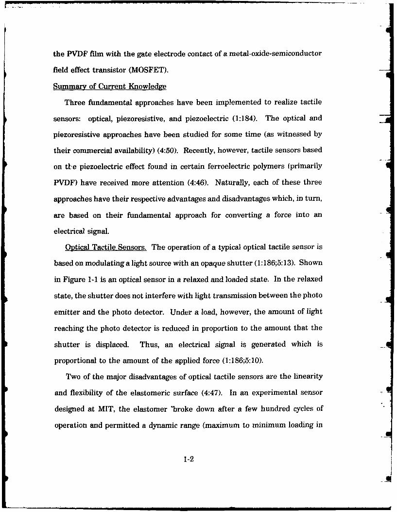
Optical Tactile Sensors. The operation of a typical optical tactile sensor is
based on modulating a light source with an opaque shutter (1:186;5:13). Shown
in Figure 1-1 is an optical sensor in a relaxed and loaded state. In the relaxed
state, the shutter does not interfere with light transmission between the photo
emitter and the photo detector. Under a load, however, the amount of light
reaching the photo detector is reduced in proportion to the amount that the
shutter is displaced. Thus, an electrical signal is generated which is
proportional to the amount of the applied force (1:186;5:10).
Two of the major disadvantages of optical tactile sensors are the linearity
and flexibility of the elastomeric surface (4:47). In an experimental sensor
designed at MIT, the elastomer 'broke down after a few hundred cycles of
operation and permitted a dynamic range (maximum to minimum loading in
1-2

the sensor's linear region) of only 18 to 1 [N]" (4:47). A major advantage,
however, is that they are currently commercially available (4:50;5:10).
Tactile Array Single Site
Stnzue
Mo Detectter
zt-z A- ran Afodende ikiLetbb
Figure 1-1. Optical Tactile Sensor (5:13).
Piezoresistive Tactile Sensors. Piezoresistive sensors are based on the
principle that the resistance of certain materials change when pressure is
applied to them (1:193;4:48). In the example shown in Figure 1-2, the actual
sensing element is the silicon diaphragm. The resistance of this diaphragm can
be measured between the two gold-plated pads. The major disadvantages of
piezoresistive tactile sensors include: high electrical noise, moderate
1-3

hysteresis, low sensitivity, and long response time constants (4:48). Again, a
major advantage is that they are commercially available (1:185;4:50)
Fo
Madm
Me 7o- ,
Figure 1-2. Piezoresistive Tactile Sensor (4:51).
Piezoelectric Tactile Sensors. Although optical and piezoresistive sensors
are commercially available, their disadvantages prompted the investigation of
an alternative sensing technique. An experimental tactile sensor (developed
at the University of Pisa) that showed great promise was based on the
piezoelectric effect (see Table 1-1) (1:198). Since this research is concerned
with developing piezoelectric tactile sensors, they are discussed in detail in
Chapter II. However, some of the major advantages of piezoelectric tactile
sensors include: high durability, low cost, high conformality, and high spatial
resolution (1:196). The major disadvantage, though, is that static pressures are
difficult to measure with piezoelectric tactile sensors because induced charges
tend to dissipate after a short period of time which results in a limited steady-
state response (1:196).
1-4

Problem Statement
A piezoelectric tactile sensor using PVDF film will be fabricated from a two-
dimensional array of aluminum electrodes that also serve as the gate electrode
contacts to discrete MOSFETs. The MOSFET electrode arrays will be designed
using in-house computer-aided design (CAD) tools, and then fabricated by the
Metal-Oxide-Semiconductor Implementation Service (MOSIS), a cooperative
group of silicon foundries which fabricate integrated circuits for education and
research. The fabricated circuits will then be coupled to a homogeneous
sample of the piezoelectric PVDF film. The resulting tactile sensors (which
differ by the PVDF film thickness used) will be tested and their performance
compared.
Table 1-1. Tactile Sensor Comparison (1:185).S patial
Approach Resolution Sensitivity Range Status
Optical 1.8 mm 3 gm 0-681 gm Commercial
Resistive 1.3 mm 230 gm 0.2-5 Kg Commercial
Resistive 2 mm 10 gm 10-1K gm Commercial
Piezoelectric 3 mm 20 gm 20-80K gm Experimental
Assumptions
The following assumptions were made:
1. The ICs fabricated by MOSIS, although manufactured by a specific,
undetermined vendor, are representative of all the MOSIS vendors.
2. Electrical fringing effects can be neglected when the electrode
separations are 5 times greater than the PVDF film thickness.
1-5

3. The average spatial resolution of the human fingertip, as reported in the
literature, establishes the minimum sensor element density.
4. The thickness of the adhesive used to attach the PVDF film to the IC
is negligible so that the electrical effects of the PVDF film dominate.
This research will be limited to an investigation and performance
characterization of the pressure sensitivity and coupling (mechanical and
electrical) of several sensor configurations. The critical variables will be the
PVDF film thickness and electrode spacing (by examining the response
between neighbors of varying distance). Other par&neters, such as
temperature, electrode size, and long-term performance will be left to future
studies.
Approach
The basic approach consists of three fundamental stages: design,
fabrication, and performance evaluation. The general steps are listed below.
Design.
Desig of the Sensor Electrode Array. The overall dimensions of the
electrode array will be 6O00x6000m (due to chip size constraints). Each
square electrode (since the VLSI CAD program, Magic, only deals with
rectangles, circular objects are very difficult to construct) will be separated
(edge-to-edge) from neighboring electrodes by a minimum of 600Lm (so fringing
effects can be neglected). A 5x5 electrode array, given these restrictions, will
have a spatial resolution approximately 4 times greater than that of the adult
human fingertip (6:205). MOSIS fabricated MOSFETs will have their gates
1-6

connected to the electrodes, and their drains and sources connected to external
pads. An additional pad will permit external biasing of the sensing electrode
to establish a consistent initial condition on the PVDF film (which was a
possible cause of the fluctuations reported in Pirolo's research) (7:5.9-5.11).
Design of the Loading Test Probe. This probe will be used to compare
the force and pressure sensitivity of the tactile sensors (1g to 100g weight
distributed over the 0.36mm 2 surface area of each electrode). This situation
correlates with pressures spanning of 0.28 N/cm2 to 28 N/cm2 .
Fabrication. Both the integrated circuits and the loading test probe will
be fabricated by outside agencies. The ICs will be fabricated by MOSIS using
the design created with Magic (8). The loading test probe will be fabricated
by the AFIT Model Shop. The tactile sensors will be constructed using four
basic steps: charge removal, adhesive application, compression baking, and bias
voltage connection.
Test and Evaluation. The performance of the sensor arrays will be tested
with the mechanical load test probe and the electrometer (the data will be
recorded on a data collection computer using a GPIB interface). The first
phase of evaluation will characterize the performance of the integrated circuits.
In the second phase, the PVDF will be tested to insure that it generates the
proper signals. The third phase will focus on the evaluation of the
performance of the assembled tactile sensors (both individual elements and
coupling effects between elements).
Through these tests, the pressure sensitivity of individual sensor elements
will be quantified, the coupling (electrical and mechanical) between them will
1-7

be established, the feasibility of using the MOSFETs as high impedance
amplifiers will be documented, and the effectiveness of using an external
biasing voltage to minimize transitory sensor instability will be explored. The
majority of the data will be statistically analyzed and presented in a graphical
format.
Order of Presentation
Background information on piezoelectricity and piezoelectric materials is
discussed in Chapter II. Chapter III develops and extends the general
approach discussed in this chapter into more detailed steps which includes
the design rationale. Test and evaluation results and analysis are presented
in Chapter IV. Chapter V summarizes the test and evaluation results to
develop conclusions and recommendations concerning this research.
1-8

II. Backaround
Introduction
Scope. Since the purpose of this thesis effort is to design a robotic tactile
sensor based on the piezoelectric effect, a fundamental understanding of
piezoelectricity, and piezoelectric materials (specifically polyvinylidene fluoride)
is critical. In this chapter, piezoelectricity is introduced with some basic
definitions and a brief history. Following this discussion, the two fundamental
piezoelectric theories (atomic and macroscopic) are presented so that the
diverse family of piezoelectric materials can be addressed. From this
discussion, the advantages of polyvinylidene fluoride (PVDF) film are compared
to the requirements for a robotic tactile sensor, and an example of a PVDF film
tactile sensor design is examined.
Motivation. Perhaps one of the most unusual aspects of piezoelectric
materials is their versatility. They can function in three very different modes:
generator, motor, and capacitor (9:1). When used as a generator, the
piezoelectric material can change mechanical energy into electrical energy.
When used as a motor, it can convert electrical energy into mechanical energy.
Finally, since piezoelectric materials are dielectrics, they can be used as
capacitors to store electrical energy.
Definitions. Before proceeding, two definitions are necessary. First,
piezoelectricity is defined by W. G. Cady as:
• . . electric polarization produced by mechanical strain in crystals
belonging to certain classes, the polarization being proportional to the
2-1

strain and changing sign with it. This statement defines the directpiezoelectric effect. Closely related to it is the converse effect . . .whereby a piezoelectric crystal becomes strained, when electricallypolarized, by an amount proportional to the polarizing field [10:4].
A related term, pyroelectricity, is defined as "a state of electric polarity
produced on certain crystals by change of temperature.. " (10:4). An
understanding of pyroelectricity is not essential to understanding
piezoelectricity, but it does have some historical significance.
History. The history of piezoelectricity actually began with the initial
discovery of pyroelectricity in 1703 when Dutch merchants brought tourmaline
crystals back from Ceylon (10:1). Tourmalines are very pyroelectric, so when
they were placed in hot ashes, the ashes would stick to the crystals' surface.
After a period of time, the crystals would cool down and repel the ashes (10:1).
This peculiar behavior earned the tourmaline crystal the name "Ceylon
magnet" (10:1). In 1824, Brewster, who had been examining similar behavior
in crystals other than tourmaline, began using the term "pyroelectricity" to
describe this action (10:1).
It was not until 1880, however, that the Curie brothers (Jacques and
Pierre), who were investigating the relationship between pyroelectricity and
crystal symmetry, found a similar relationship with pressure (9:2;10:2). Thus,
they became the "fathers" of piezoelectricity.
The Curie brothers initially discovered that an electric field was generated
by an applied mechanical stress (or the direct piezoelectric effect). In 1881,
Lippman proposed the converse effect, which was immediately verified by the
Curies (9:2;10:4).
2-2

In the following years, a number of scientists began refining the theory of
piezoelectricity. Foremost among them was Woldemar Voigt who, in 1910,
published his celebrated work, Lehibuch der Kristallphysik, where he showed
which of the 32 crystal classes would be piezoelectric (and what piezoelectric
i• constants would be nonzero) (10:5).
Once the piezoelectric effect had been quantified for a number of materials
(particularly quartz and rochelle salt), other scientists began applying the
* •piezoelectric effect to solve various problems. One of the first scientists to find
a practical application for piezoelectricity was Langevin. During World War I,
he developed a way of locating submarines by interrogating submersed objects
with high frequency (ultrasonic) waves. Consequently, he provided the
groundwork for the science of ultrasonics (9:2;10:5).
After Langevin, there was a flurry of activity and research associated with
piezoelectric crystals, ceramics, and organic materials. This research
culminated in the piezoelectric thin film materials that are finding their way
into a plethora of applications today (11:2-3).
Piezoelectricity
In order to gain an appreciation for the operation of piezoelectric devices,
it is necessary to have an understanding of both the physics describing the
piezoelectric effect (atomic analysis), and the origin of the piezoelectric
constants (macroscopic analysis). The treatment here will be necessarily
simplified and condensed. A more thorough analysis can be found in W. G.
Cady's book, Piezoelectricity (10).
2-3
I

Atomic Analysis. Fundamental to an understanding of the atomic analysis
of the piezoelectric effect is the concept of a center of inversion (or a center of
symmetry) (7:2.7;9:1;12:7). A center of inversion permits non-piezoelectric
crystals to maintain an overall neutral charge when stressed (see Figure 2-1a).
Thus, the basic reason why certain crystals are piezoelectric is that they lack
this center of inversion (7:2.7;9:1;12:7). When pressure is applied to an
asymmetric crystal, the crystal becomes polarized and creates an electric field
(see Figure 2-1b) (7:2.7).
0- (!- )0(b
I Center of,o . . Inversion
L ---------
STRESS Center of
O Inversion ( STRESS
2-4
+STRESSSTRESS
Figure 2-1. Concept of a Center of Inversion in a CrystallineStructure. (a) Crystal with a Center of Inversion, and (b)Crystal without a Center of Inversion (7:2.7).
2-4
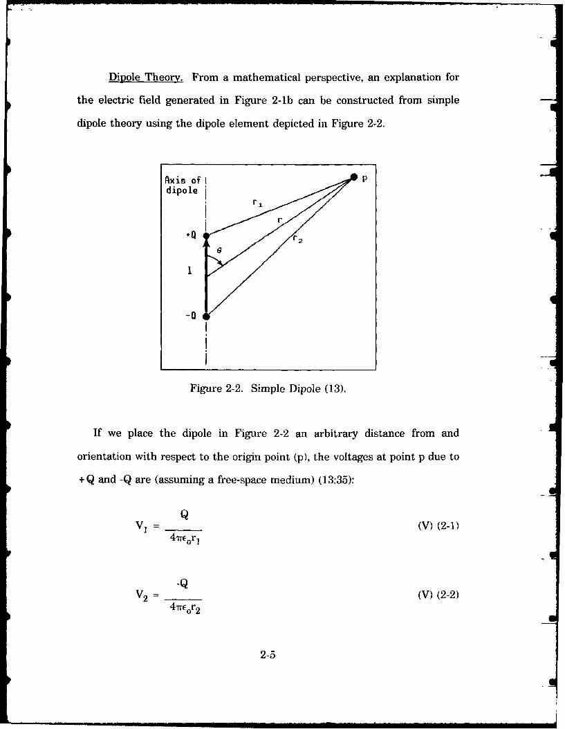
Dipole Theory. From a mathematical perspective, an explanation for
the electric field generated in Figure 2-lb can be constructed from simple
dipole theory using the dipole element depicted in Figure 2-2.
Axis of I r -dipole i
ir+0 r2
-0
1
Figure 2-2. Simple Dipole (13).
If we place the dipole in Figure 2-2 an arbitrary distance from and
orientation with respect to the origin point (p), the voltages at point p due to
+Q and -Q are (assuming a free-space medium) (13:35):
QV 1 = (V) (2-1)
-QV2 = (V) (2-2)
4 -7rE 0ro2
2-5
where Q is the fundamental unit of charge, and Eo is the dielectric constant of -
free-space.
Using the principle of linear superposition, the total voltage observed at
point p is (13:35):
VTOT = V1 + V2 = (V). (2-3)4-ire0 r 1 r 2
For r much greater than the charge separation (1) (see Figure 2-2), the
distances between p and each of the charges can be approximated by (13:36):
lcos(0)r1 = r - (m) (2-4)
2
lcos(O)r 2 = r + (m). (2-5)
2
The total voltage can then be re-written as:
Qlcos(O)VTOT = (V). (2-6)
47eo[r 2-(0.25) 2cos 2 (0)]
2-6
Since r is much greater than 1, the 12 term in the denominator can be ignored.
Thus (13:36):
Qlcos(0)VTOT = (V). (2-7)
4,E 0r2
By definition, the electric field is the negative gradient of the voltage
(13:35). Therefore, the electric field is (in polar coordinates) (13:36):
Qlcos(0) ^ Qlsin(0)E = r + 0 (V/m). (2-8)
2 rEor 3 41rEor 3
Dipole Theory Applied to Crystals. As an example, consider the crystal
shown in Figure 2-3. In its equilibrium state (Figure 2-3a), there is no net
electrical field. When the crystal is strained as shown in Figure 2-3b, however,
the net electric field becomes:
Q1E = 0 (-0.155) (V/m) (2-9)
47rrE 0r 3
where 1 is the distance between the central (negative) ion and any of the
positive ions, and r is the distance to the point of observation.
2-7

120 20 115 1150
to9+'0 + Q A .
1 0.1280 1380(a) (b)
Figure 2-3. Example Crystal in Two States. (a) Equilibrium and (b) Strained(7:2.9).
This simple two-dimensional case illustrates how some of the early
piezoelectric researchers were able to predict which of the 32 crystal classes
would be piezoelectric.
Although the atomic view is a convenient way to understand the nature of
piezoelectricity, it is difficult to predict a given crystal's exact behavior using
atomic theory. The reason for this dilemma has been discussed by Cady in his
book, Piezoelectricity:
In spite of the fact that molecular or atomic theories of piezoelectricitybegan to appear very soon after the Curies' discovery, a satisfactorytheoretical treatment of the phenomenon can hardly be said to havepassed the initial stage. The resources of modern lattice dynamics arestill unequal to the task of predicting anything better than a roughapproach to the order of magnitude of the piezoelectric effect, even for Athe simplest structures [10:7311.
2-8

I ,I iI ~I.. up ., l!i. .... . .
Therefore a larger, macroscopic view was adopted to establish useful
predictions about a piezoelectric crystal's behavior.
Macroscopic Analysis. The macroscopic nature of piezoelectricity and the
piezoelectric coefficients are based on three fundamental physical properties
of a crystal: stress, strain, and polarization (10:178).
Stress. The stress applied to a crystal's surface has the units of force
per unit area, and has six degrees of freedom (three normal stresses and three
shearing stresses) (9:21;10:47). Figure 2-4a is a normal stress, while
Figure 2-4b depicts a shear stress. Stresses will be represented by the letter
'X' with a subscript spanning between one and six, that corresponds with each
of the degrees of freedom (7:2.12):
Xx' Yy, Zz, Yz, Zx, Xy = X1, X2, X3 , X4, X5, X6 (N/m 2). (2-10)
The upper-case letters on the left side of Eq (2-10) denote the direction of the
force, and the subscript represents the normal to the surface to which the
force is being applied (7:2.14;10:47).
Strain. Strain is the relative deformation of a crystal under an applied
stress (7:2.14;10:47). It is similar to stress since it has six degrees of freedom; -
however, because it is a ratio, it is unitless. Strain will be represented by the
letter 'S' with a subscript having a value between one and six (7:2.15):
X, Yy, Zz, Y, Zx, = S1, $21 S3 , S4 , S5 , S 6 (unitless). (2-11)
2-9
• i.lll i ii l al li I i .ms.e...

Like stress, the subscripted letters indicate the direction of the normal to the
crystal's surface to which the force causing the strain is being applied. The
other letters (x, y, and z) represent the direction of the applied force (10:47-
52).
F (a)
1 x
F
Figure 2-4. Stress Types. (a) Normal Stress and (b) Shear Stress(7:2.14).
Polarization. Polarization differs from stress and strain in that it only
has three degrees of freedom (there is no such thing as a "shearing"
polarization). It is represented using the letter 'P' with a subscript spanning
between one and three (7:2.18).
P1 = x-directed polarization
P 2 = y-directed polarization (C/m 2). (2-12)
P 3 = z-directed polarization
2-10

General Elastic Crystal Equations. For a generic crystal (not
piezoelectric), the stresses and strains are related by Hooke's Law
(7:2.16;10:48):
6 6Si =i Y Sik Xk (unitless) (2-13)
i k
6 6Xi Y- Cik Sk (N/m 2 ) (2-14)
ik
where Sik is the elastic compliance coefficient, and Cik is the stiffness coefficient
(7:2.17).
Furthermore, the polarization of a crystal is directly related to the applied
electric field (7:2.18;14:511):
3 3Pm = X3 im E
(C/m 2) (2-15)M i
where Eim is the dielectric constant, and Ei is the applied electric field.
These equations pertain only to non-piezoelectric materials since, if the
crystal were piezoelectric, Eqs (2-13), (2-14), and (2-15) would take on extra
terms.
Piezoelectric Crystal Equations. The additional terms in the
piezoelectric equations stem from the fact that in a piezoelectric crystal, a
mechanical strain generates a polarization (the direct effect). Similarly, for the
converse effect, an electrical field generates a stress. The direct piezoelectric
effect can thus be represented by (7:2.18;10:183):
2-11

6 3Pr = 1: dmiX + XXkm Ek m = 1,2,3 (C/m 2) (2-16)
k
where dmi is the piezoelectric strain constant, and the superscript X refers to
a constant strain.
Furthermore, the converse effect can be represented by (7:2.18;10:183):
6 3Si = Yx sEik Xk + X. dmi Em i = 1,2...5,6 (unitless) (2-17)
k m
where the superscript E in sEik refers to a constant electric field.
The electro-mechanical coupling factor (k) indicates the energy conversion
efficiency of a particular piezoelectric material. It is the ratio of the energy
generated (mechanical or electrical) to the energy provided (electrical or
mechanical) (15:10). Oftentimes, the coupling factor will be subscripted to
indicate the direction of the applied energy and the location of the electrodes
(11:18). A numbering convention of x=1, y=2, and z=3 is used for the
subscripts (11:9). As an example, k13 means that the coupling factor was
measured with electrodes perpendicular to the 1 (or x) direction, and the strain
was induced in (or applied to) the 3 (or z) direction (this numbering convention
is also used for the piezoelectric strain coefficient). Typical values of the
electro-mechanical coupling factor range from zero (non-piezoelectric) to almost
unity.
2-12

With an understanding of the origin of the piezoelectric coefficients and
the definition of the electro-mechanical coupling factor, comparisons between
various piezoelectric materials can be made.
Piezoelectric Materials
Early Materials. Two of the earliest materials used in piezoelectric devices
were quartz and rochelle salt. This was probably due to their relative
abundance (quartz occurs naturally, and rochelle salt was used for medicinal
purposes) (9:114).
Rochelle Salt. Rochelle salt has a very high coupling factor (0.9).
Unfortunately, it suffers from environmental restrictions because of its
composition (which consists of a significant amount of water) (9:115). The
chemical formula for rochelle salt is NaKC4H4 06.4H20, and the water
molecules are an integral part of its structure (9:115). If the environment
changes, the crystals' performance will be degraded. That is,
... if the humidity of the surrounding atmosphere is below 35 per centat 25°C, the water vapor pressure of the crystal is greater than thevapor pressure of water in the surrounding atmosphere and the crystalwill lose water and dehydrate. . .Above 85 per cent humidity, the crystalwill absorb water from the atmosphere on its surface and will slowlydissolve if kept in such an atmosphere [9:117].
Therefore, care must be taken when using rochelle salt in uncontrolled
environments. One way to minimize the effects of the environment is to place
the crystal (with its electrodes attached) into a hermetically sealed container
along with both powdered and dehydrated rochelle salt (9:117). Consequently,
the humidity stabilizes at the desired range for proper operation of the
rochelle salt crystal.
2-13

W* gu _. 111 ll E= l I I - -iii - " lE J J I - w Ip 1..
The piezoelectric efficiency of Rochelle salt is also strongly temperature
dependant (9:129). It only functions effectively in the temperature range of
-18°C to 24*C (9:117). Because of these environmental constraints, rochelle
salt was primarily used as a transducer at low-frequencies (9:114).
Quartz. Since quartz does not require water molecules in its crystal
matrix, it has a major environmental advantage compared to rochelle salt.
Unfortunately, its coupling factor is only on the order of 0.1 (15:10). In spite
of its low coupling factor, it does make a very stable oscillator element, which
explains its widespread use in watches and other time-dependent devices
(9:78).
Ceramics. Piezoelectric ceramics would have seemed an impossibility to
researchers prior to World War II since a ceramic is a conglomeration of
random crystallites (see Figure 2-5) (15:1). However, in 1946, a method for
transforming a polycrystalline material into a piezoelectric material was
discovered:
... the polarity needed to impart piezoelectric properties can be givento an originally isotropic polycrystalline ceramic, more or lesspermanently, by temporary application of a strong electric field. Thisprocess, called "poling", is analogous to the magnetizing of a permanentmagnet [15:1].
Poling, then, refers to the application of an intense direct current electric
field across the ceramic. This field tends to align the polarization axes of the
crystallites in the ceramic, thus rendering it piezoelectric.
2-14

One of the first piezoelectric ceramics extensively investigated was barium
titanate since it possessed a higher coupling factor compared to the other
known piezoelectric materials (except for rochelle salt) (15:53). The basic cell
of barium titanate (as well as most other piezoelectric ceramics) is the
Perovskite structure shown in Figure 2-6 (15:53).
loum
Figure 2-5. Barium Titanate Crystallites (15:65).
2-15
...... .... .... ... . .... . . . . . -,] i, , n i I mm l lm lll a1111 r- - --

When the coupling factors of a pure crystal of barium titanate are compared
with the ceramic version (see Table 2-1), there is a noticeable difference. This
difference is attributable to the fact that "the anisotropy is much smaller for
the poled ceramics than for a single crystal" (15:72).
~Barium aygen Q Titanium
Figure 2-6. Perovskite Structure (15:49).
2-16

Table 2-1. Barium Titanate Coupling Factors (15:74).
CouplingFactor Ceramic Crystal
k15 0.476 0.570k31 0.208 0.315k33 0.493 0.560
Organic Polymers. The poling process is also fundamental to piezoelectric
organic polymers. Among them is the polymer polyvinylidene fluoride (PVDF).
In 1969, Kawai determined that polarized PVDF "developed far greater piezo
activity than any other synthetic or natural polymer" (16:975). PVDF can be
polarized in a manner very similar to the process used to make ceramics
piezoelectric (poling) (11:5).
Fabrication. In order to make poling effective, however, it is necessary
to align as many of the polymer chains as possible. This result is accomplished
by stretching the material into thin sheets. Because of this step, PVDF films
cannot be made very thick. Typical thicknesses range between 9 and 800
microns (11:14). After stretching the PVDF film, it is necessary to pole it to
turn it into a piezoelectric material.
The predominant phase in the stretched PVDF film is the non-polar a-
phase (see Figure 2-7a) (12:26-27). Since the polarized (and hence,
piezoelectric) p-phase is the preferred phase (see Figure 2-7b), the PVDF sheet
must go through a poling step to convert as many of the a-phase crystallites
into the P-phase (see Figure 2-8) (12:27).
Disadvantages. One of the major disadvantages of PVDF film is its
sensitivity to extreme temperatures (80'C to 120'C). When the PVDF film
2-17

I I ! I . . . . l l .w _ I I I -! ! I , , . •
7J
reaches these temperatures, mechanical relaxation in the material degrades
its piezoelectric activity (12:51).
Other disadvantages of PVDF film compared to traditional piezoelectric
materials include: a relatively low coupling coefficient (0.19), sensitivity to
electromagnetic interference, and the relative thinness of the films -
(7:2.25-2.26). Despite these disadvantages, PVDF film has found its way into
a myriad of applications because it possesses many other desirable
characteristics.
Alpha Beta
Figure 2-7. PVDF ot-and p-Phases. The small white spheresrepresent hydrogen atoms, the larger white spheres representcarbon atoms, and the cross-hatched spheres represent fluorineatoms (12:27-28).
2-18

Advantages. The major advantages of PVDF film compared to
conventional piezoelectric materials include (7:2.24-2.25):
1. The film can function over an extremely wide frequency range (DCto approximately 10MHz).
2. It has a low acoustic impedance. (This feature makes it a goodimpedance match for medical ultrasound and hydrophoneapplications.)
3. The film possesses a higher dielectric strength than piezoceramicmaterial (30 V/micron versus 1.5 V/micron) and, therefore, can beexposed to higher electric fields.
4. The film has a relatively high electrical impedance. (This advantageallows the film to provide a complimentary match to high-impedancedevices (for example, CMOS) and circuits.)
5. Since the film is thin and flexible, it can be laminated to a vibratingstructure without significantly distorting the motion of the structure.
6. Because the film is a high molecular weight fluoropolymer, it ismechanically strong and resistant to extreme environmentalconditions (most solvents, acids, oxidants, and ultraviolet radiation).
7. The film can be cut and formed into complex shapes or prepared asa large transducer area.
8. The material and fabrication costs of the film are generally lowerthan those of other piezoelectric materials.
These attractive properties make the disadvantages of PVDF film tolerable,
and thus, it is an ideal candidate for a wide range of piezoelectric devices.
PVDF Film Tactile Sensors
One of the recent applications of PVDF film has been in the arena of tactile
sensors (11:37). PVDF film is an appropriate piezoelectric material to use in
this application since its advantages strongly correlate with the basic
requirements and considerations of an ideal tactile sensor.
2-19

I ........
poling
voltage~poling
direction
Figure 2-8. PVDF Poling (12:29).
Considerations. Several of these considerations include (but are not limited
to) the following factors. First, in order to function in a human environment,
a tactile sensor should possess the spatial resolution of the human fingertip .
(4:46;6:200-201). Secondly, since the initial application of these sensors will
probably be in industry (where robots are used in hazardous environments),
the sensor material should be relatively inert. Thirdly, it should have a
bandwidth of at least DC to 100 Hz (for the control loop requirement) (4:46).
Finally, it would be desirable to have the sensor perform low level integration
of the inputs in order to minimize the information traffic to the central
processor (17:82).
All of these objectives can be realized with a PVDF film tactile sensor. The
spatial resolution of a human fingertip (see Figure 2-9) can be achieved simply
by patterning an array of electrodes on the surface of the film. The stability
of PVDF film in hazardous environments has been discussed along with its
2-20

frequency limitations. Finally, since PVDF film is available in thin sheets, the
material can be applied directly to either a printed circuit board or a silicon
substrate where sensing, amplification and signal processing can be
accomplished (4:51).
• 0 •20 •
e . a Rol* F ertp (
th~ ~Fiue 2-9. P fl a e uvale Sparae ytioaleslu rsition ofer(ue
for thermal sensing purposes) and a flexible layer (4:52).
2-21

The flexible layer between the two piezoelectric layers serves to make the
outer layer more sensitive by flexing, thereby creating more strain in the
epidermal PVDF film layer (4:52). The electrodes can be realized using a
metallization technique, a conductive epoxy, or a conductive metallic adhesive
tape. Finally, in addition to providing a support structure for the sensor, the
backing can serve to locate the sensing, amplification, and integration circuitry.
Conclusion
Piezoelectricity, the conversion between mechanical energy and electrical
energy, has a fascinating history. From the discovery of tourmaline to the
development of piezoelectric polymers, scientists have explored the
fundamental properties of piezoelectricity, and attempted to explain them in
various ways.
The physical theory of piezoelectricity (in the atomic view) is based on the
relatively simple dipole theory, while the macroscopic (and more pragmatic)
analysis establishes the piezoelectric constants and the coupling factc" in terms
of stress, strain, polarization, and Hooke's Law.
With an understanding of piezoelectric theory, various piezoelectric
materials can be discussed and compared. Ranging from the early materials
* (quartz and rochelle salt) to the more recent materials (ceramics and
polymers), all of the piezoelectric materials have advantages and disadvantages.
The advantages of the PVDF polymer can be used as the basis of a robotic
tactile sensor. A PVDF film tactile sensor can be configured to possess the
spatial resolution of the human fingertip; and the sensor can be coupled to
2-22

either a PC board or an integrated circuit which incorporates sensing,
amplification and signal processing circuitry.
Conductors
Protective -O EpidermalLayer -Sensor
oDermal1Sensor
0 ' Resistive 'Coating'
Metal SPVF Film Square MetalPlate /W Er- Plate
Printed CircuitBoard
Figure 2-10. Sample Tactile Sensor (4:52;7:2.53).
2-23

II. Experimental Procedures
Introduction
In order to accomplish the goal of realizing a tactile sensor, a number of
items must be designed and fabricated (the integrated circuit, a loading test
probe, and a test board). In addition to the design of the sensor's hardware,
of parallel importance is the development of a method for testing the tactile
sensor and its subcomponents. The design and fabrication of the hardware and
the basic test plan is presented in a chronological order, starting with the
design of the integrated circuit and ending with a completed test plan.
Integrated Circuit
The design of the integrated circuit was influenced by a number of factors
which included the design of the electrodes, investigation of signal propagation
delays, and the design of the sensor amplifiers. In order to design and
fabricate an integrated circuit in a reasonable period of time (less than three
months), it was decided that MOSIS would fabricate the ICs from a design
accomplished with AFIT's CAD tools and submitted electronically. To further
increase the probability that the returned circuits would be operative (since
there was no way of controlling any of the processing steps), and to reduce the
cost of the sensor (since submicron geometry features were not required), the
3 micron MOSIS technology was selected (the largest feature size and most
inexpensive MOSIS technology).
3-1

Electrode Size. The size of the IC sensor element electrodes was based on
two important factors, the spatial resolution of a human fingertip (the
minimum distance between two points before they become indistinguishable
from a single point) and the amount of real-estate available on a MOSIS
fabricated integrated circuit. Since the largest feasible IC size was limited to
an area of 7900mX92001m, and a portion of the area had to be reserved for
the amplification circuitry, the area available for the electrodes was limited to
a 6000mx6000.m square centered on the IC (see Figure 3-1).
,6000 jrm
Figure 3-1. Integrated Circuit Partitioning.
Furthermore, in order to minimize the degree of electrical and mechanical
coupling between discrete sensor elements, a 5x5 sensor array was utilized,
whereby individual electrodes were separated from their nearest neighbors by
a distance equal to the edge length of a square electrode array element.
Twenty-five electrodes (600pmx6Opm each) in a 6000pmx6001m square
3-2

corresponds to a spatial resolution that is approximately four times greater
than that of the human fingertip (6:205).
This choice of electrode size affected the voltage generated by the PVDF
film since voltage is related to area by V = (qt)/(EA) where q is the charge
generated by the PVDF film, t is the thickness of the PVDF film, E is the
permittivity of the PVDF film (E = EoE), and A is the area of the sensor
electrode (13:70). The worst case would be the voltage generated by the
thinnest (25jLm thick) film with an applied weight of ig (an applied force of
0.01N). This force distributed over an area of 600pLmx600pLm should generate
approximately 0.1V (from Appendix C, d33 = 16pC/N so q=0.16pC, and ,= 11).
The maximum voltage would be generated by the thickest (110Pm thick)
film with an applied weight of 100g (an applied force of IN). This
configuration will produce a voltage at the sensor electrode of approximately
50V (this assumes that there are no charge saturation effects; that is, an
unlimited supply of charge carriers).
Line Length Considerations. When connecting the electrodes to the
amplifiers, two interconnect strategies were evaluated. The first used a direct
route to the amplifiers, and the second was devised to insure that the electrical
length of each electrode/amplifier interconnect was identical. Obviously the
simplest approach is to use the direct route. However, if the difference in
signal propagation delays between the electrodes becomes significant, the
second method is preferable. In order to make the determination of which
method to use, a simple calculation was accomplished based on the typical
3-3

interconnect resistance and capacitance parameters characteristic of 3 Lm
feature size integrated circuits.
Assuming an interconnect length of 4000pm (a maximum value in the IC
design), a conductor width of 6 m, a capacitance between the metal layer and
the substrate of 1x10 "4 pF/pm 2 , and a sheet resistance (for aluminum) of
0.05i/square, the resistance of the line would be approximately 33f, and the
capacitance would be about 2.4pF (18:121,135). This results in an RC time
constant of roughly 80 pico-seconds. This time constant was considered
insignificant, so the direct wiring route was adopted.
Amplifier Design. In order to achieve a gain greater than unity for the in
situ amplifiers, two inverting amplifiers were used. Although a single stage,
non-inverting amplifier was desii ed (as the PVDF film response increases, the
output of the amplifier should increase), a single-stage non-inverting amplifier
would only have a maximum gain of unity. Therefore, two inverting amplifiers
were placed in series. The preliminary design is shown in Figure 3-2.
This amplifier was modelled in Spice using the default three micron feature
size MOSIS models to determine appropriate resistor values (19). Since
process parameters could vary between the default Spice model and the actual
fabricated amplifier, the amplifier was designed so that its linear region would
be centered on 5 volts (for a 1OV Vdd). The approximate minimum voltage
generated by the PVDF film was calculated to be 0.1V (see page 3-3), so the
output voltage with a gain of 5 in the linear region (see Figure 3-3) would be
0.5V (which should be detectable by external measurement devices). The
linear amplification region is approximately 2V wide (see Figure 3-3). N-type
3-4

-- --
MOSFETs were used because electrons possess a higher mobility and this
feature manifests itself in a larger gain per transistor area (18:40-41). The
MOSFET geometry used incorporated a 3pm gate length and a 12im gate
width.
Vdd
5K Ohms 5K Ohms
In Out
Figure 3-2. Schematic of the DiscreteSensor Element Amplifier Design.
The resistors were designed using an n-diffusion so that they could be
placed in the same well as the transistors. A sheet resistance of 25fl/square
was assumed for the n-diffusion (18:121). In order to create a 5KfI resistor
(from the Spice analysis), 200 squares were required. Consequently, a resistor
was created that was 4.5 m wide and 900 pm long (see Figure 3-4).
To minimize the line resistance and capacitance, the amplifier should be as
close to the sensor electrode as possible. However, since the electrodes will be
beneath a layer of PVDF film, it would make testing difficult (since there
would be no direct access to the electrode signal, or to the amplifier).
3-5

Therefore, a compromise was attained, and the amplifiers were placed on the
periphery of the integrated circuit (see Figure 3-5).
I t_ ISK -
~~ I___ __IF - -------
7 '
8 8 1O
Figure 3-3. Spice Plot of Amplifier Characteristics.
For subsequent testing and verification of the amplifier characteristics, it
was important to place sufficient pads to permit separate testing of each
component (two MOSFETs and two resistors per amplifier). With the three
pads shown in Figure 3-4 (and the Vdd and ground pads shown in Figure 3-5),
it is possible to test each resistor and transistor.
3-6

clfplot* Window. -36751 252*3 -121S8 41S58 --- ScC19 I micron in .315 inches (381K)
: Input•Test TestPad ,Pad
.9,J
.............. .. .. -------_ _.__._.w, i
MO SFE T
Resistor
OutputBonding
Pad
Figure 3-4. Caltech Intermediate Form (CIF) Plot of the Tactile Sensor'sAmplifier.
Bias Voltage Considerations. Since the minimum signal generated by the
PVDF film should be near O.1V (see page 3-3), a bias voltage is required to
bring the signals into the linear region of the amplifier. The easiest way to
3-7

Li
accomplish this objective is to provide a resistor network on the input of the
amplifier (20:397-400). The disadvantage with using this method, however, is
that placing a relatively low resistance (compared with the high gate-to-
substrate resistance of the MOSFET) between the electrode (which is the
signal source) and ground would defeat the objective of using a MOSFET as a
high input impedance amplifier, and would further attenuate an already small
amplitude signal.
An alternative scheme was devised to provide a biasing voltage for the top
surface of the PVDF film. Since PVDF is a polar dielectric, the biasing voltage
will be transferred to the electrode on the bottom of the film through the
PVDF dipole moment after the system has equilibrated (13:35-37).
MOSIS CIF Submission. The complete layout for the integrated circuit is
shown in Figure 3-5. The two vertical amplifier strips on either side of the
circuit are electrically isolated, so the second strip can be used if one strip gets
damaged. Located at each of the four corners are large pads which can be used
to bias the top layer of the PVDF film. The entire electrode array is
surrounded by alignment marks to facilitate locating particular elements after
the array is covered with the PVDF film (that is, for proper placement of the
loading test probe). The pads on the extreme left (16 pads) and right (17 pads)
are the bonding pads. Should the IC behave as anticipated, these pads will
permit testing of the IC without any probes. Also, the two sides without
bonding wires will permit mounting the PVDF film and minimize damaging
the delicate wire bonds. This layout was created using the Magic VLSI circuit
3-8
00

editor and converted to a CIF file which was then sent to MOSIS (8). The
Magic file is listed in Appendix D.
Amplifier Strip Sensor Electrode
WWWH Vdd
.~~~.......: ...-i ...
Alignment Bias Voltage) ND
Mark Pad
Figure 3-5. Caltech Intermediate Form (CIF) Plot of the Integrated Circuit.
Test Probe
Minimum and Maximum Loading Forces. The minimum and maximum
test probe loading forces were derived from a suggested minimum force of
10 2N applied over an area of 1x10 -6 m2 , and a suggested maximum force of
3-9

ION applied over the same area (6:201). These parameters equate to a
minimum weight of 3.7g applied over a discrete electrode area (6001imx600pm),
and a maximum weight of 3.7Kg applied over the same area (assuming a
gravitational acceleration of 9.8m/sec 2).
The maximum weight seemed a bit unrealistic (it is similar to
administering a 3Kg weight via a pencil point to the human fingertip) and
would also be difficult to keep aligned over the small geometries of the tactile
sensor. The maximum weight was therefore reduced to 100g (and the
minimum weight was reduced to 1g).
Alignment Considerations. It was also necessary to determine, within the
width of one electrode (600 m), where the loading probe would make contact,
so a means of aligning the probe with respect to the tactile sensor's surface
was devised. Rather than designing a relatively complex alignment
mechanism, an existing instrument was identified; that is, a micromanipulator
was used with an IC microprobe station. A loading probe sub-assembly, which
was compatible with the micromanipulator arm, was then designed.
Microprobe Sub-Assembly. A diagram of the microprobe sub-assembly is
shown in Figure 3-6 along with a loading weight (50g when made out of lead).
Since the loading probe was fabricated from aluminum, it should weigh
approximately 2g (based upon the volumetric density of aluminum).
Actual Minimum and Maximum Weights (Calibration). The loading probe
and three weights were fabricated in the AFIT Model Shop. When they were
returned, the entire system (micromanipulator and loading test probe with
zero, one, two and three weights) was calibrated.
3-10

PROBE Aluminum
7.5cm
0cmm-07om .5c.07c
0.5cm
1.25cmm
TT
1.2.8cm
Figure 3-6. Microprobe Sub-Assembly.
3-11

With no weights, the loading probe presented a weight of 0.8g to a balance
located in the same relative position as that of the tactile sensor during the
test phase. With all three weights, the probe presented 76g to the balance.
These weights were slightly lower than predicted, but still sufficient for
investigating a range of weights (forces) spanning two orders of magnitude.
Test Protoboard
A protoboard was configured to provide the proper signals to the tactile
sensor IC for testing. These signals included ground (pins 9 and 42), Vdd (pins
23 and 55), and Vbias (pins 4, 8, 24, 41, and 56). The protoboard also permitted
easy access to the output signals.
LED Test Grid
In order to facilitate examining the response of the entire tactile sensor
array, and to provide a means of obtaining a qualitative feel for the operation
of the sensor, a second test board was designed and fabricated. This board
consisted of an array of LEDs connected to the output of each of the 25
amplifiers. The schematic of a single LED indicator is shown in Figure 3-7.
This board produced a visual picture of the state of the entire sensor array
without having to probe each of the outputs. This tool was invaluable during
the initial biasing phase of each test, since the LEDs displayed the same
relative brightness when the sensor elements were in a similar bias state.
PVDF Film Etching/Cutting Process
A process for etching and cutting the bulk PVDF film for subsequent tests -
was also created. The vendor procured films are available in sheets roughly
8 by 11 inches with aluminum metallization on both surfaces. Since the
3-12

required PVDF film samples had to be cut into squares the size of the
electrode array (6mmx6mm), and since they could have metal on only one side,
the following process was implemented to realize the desired PVDF material
configuration (the required materials and equipment are listed in Appendix A):
AmpOutput
330 Ohms
Figure 3-7. Schematic of a Single LEDIndicator Element.
1) A grid of 6mm by 6mm squares was created on a sheet of plain white
paper.
2) A glass-slide was placed beneath the bulk PVDF film and a section of
PVDF film was cut (using a #11 scalpel) so that it would fit within the
borders of the glass-slide. A drop of isopropyl alcohol was placed on the
glass-slide prior to the placement of the PVDF film to keep the film in
place. The top surface was marked with an indelible marker by placing
a dot in one corner (this action facilitated subsequent determination of
the polarity of the PVDF film sample).
3) The exposed metallized surface of the film was etched with a cotton
swab wetted with dilute ferric chloride (1 part ferric chloride to 10 parts
3-13

de-ionized water). The etchant was kept away from the PVDF film
boundaries since it could diffuse beneath the film. Etching through the
thin aluminum film occurred in approximately 1 to 5 minutes, and it was
marked by a distinct darkening of the etched area.
4) The PVDF film was then cleaned by rinsing it thoroughly in de-ionized
water for 2 minutes. This rinse was accomplished by removing the PVDF
film from the glass-slide. When the rinsing operation was completed, a
fresh glass-slide was used to hold the PVDF film (the PVDF film was
oriented so that the orientation dot was on the top surface). Excess
moisture was removed from the PVDF film/glass-slide assembly with a
paper towel.
5) The glass-slide was placed over the 6mm paper grid. Using the gridlines
as a guide, the PVDF film was cut into 6mm squares. A sharp scalpel
was essential, and the cuts were made as smoothly and as quickly
possible. The PVDF film squares were cut from the center (etched area)
of the film so that there was no possibility of leaving metal on both
sides of the film. The orientation dot was then transferred to each
square with an indelible marker.
6) The squares were stored dry in folded lens tissue (after insuring that the
squares were separate and had no chance of scratching each other).
Tactile Sensor Fabrication
The procedure for creating tactile sensors was developed and refined after
attempting several experimental procedures. Unanticipated problems with
3-14

charge storage on both the floating gates and the PVDF film squares damaged
some of the integrated circuits. To minimize this failure mechanism, the
following procedures were implemented to fabricate the tactile sensors from
the integrated circuits and the cut PVDF film samples (the required materials
and equipment are listed in Appendix A):
1) Since charges can be stored on the floating gate and on the PVDF film
squares, it is essential that these charges be neutralized immediately
before contacting the IC and the PVDF film squares. To neutralize these
charges, the IC was dipped into grounded water (200ml of de-ionized
water and 1 drop of concentrated HCI in a beaker with an electrical
connection to earth ground) for 1 minute. The same procedure was
accomplished for the PVDF film square. The IC was dried with nitrogen
gas carefully aimed so as not to break any of the delicate wire bonds.
The PVDF film square was dried with lens tissue.
2) A drop of the adhesive (Shipley Miroposit 1400-17 Photoresist) was
deposited on a clean glass-slide. A small amount of photoresist was then
drawn up into a 1mm glass pipette. Enough photoresist was transferred
to the IC to thinly cover the central 9 electrodes (a dissecting microscope
proved useful). The PVDF film square was carefully placed (metal side
up--verified with an ohm-meter) on the IC so that it covered all 25
electrodes. Some photoresist escaped near the PVDF film edges.
3) A compression block (made from a glass-slide cut into approximately
7mmx7mm squares with a diamond scribe, was coated with a thin layer
silicone oil. The compression block was gently placed on the PVDF film
3-15

(silicone oil between the compression block and the PVDF film) using
tweezers. Once the compression block was in place, a binder clip was
positioned so that it compressed the IC/photoresist/PVDF
film/compression-block sandwich (see Figure 3-8). The whole assembly
was placed into a 70°C oven for 20 minutes. After baking, any stored
charge was removed by dipping the whole assembly in grounded water.
Slicone Ioil Compression Block FF
F1Ceramic Case
pin PIn
Side View
Figure 3-8. IC/Photoresist/PVDF/Compression-Block Sandwich.
4) The top (metallized) surface of the PVDF film was connected to an
external pin with a 1 mil wire and silver paint. Originally, the
metallized surface would have been connected to the bias voltage pads
by placing silver paint on one or more corners of the PVDF film and
drawing the paint over the edge so that it contacted the bias voltage
pad. However, the silver paint residue is difficult to remove from the
surface of the IC. Thus, in order to conserve ICs (so that a single IC
could be used for multiple tests), a 1 mil wire provided the connection
3-16

between the metallized surface of the PVDF film and to external pin 4
(see Figure 3-9). Good electrical contact was verified by placing one lead
of a continuity checker on top of the PVDF film and another lead on pin
4 of the IC.
AWW
Figure 3-9. Fabricated Tactile Sensor.
Test and Evaluation
The final area of design was the development of a test plan which was
broken down into logically arranged sub-tests which contributed to the
3-17

knowledge concerning the performance of the components of the tactile sensor
before actually fabricating and testing the completed tactile sensor. These sub-
tests consisted of an integrated circuit test, a PVDF film sample test, and a
complete tactile sensor test (the materials and equipment used in these tests
are listed in Appendix A).
Integrated Circuit Testing. The purpose of this test was to verify proper
operation of the fabricated ICs (insuring that the vendor did not make any
fabrication errors) and to validate the design by amplifying controlled test
signals. This test was compartmented into 4 major areas: MOSFET tests,
resistor tests, amplifier tests and sensor element interconnection tests.
MOSFET Characteristics. The MOSFETs were tested by randomly
selecting several MOSFETs from various ICs and connecting the gate, source,
and drain (using the probe pads and the microprobe station) to a
semiconductor parameter analyzer (Hewlett Packard Model HP 4145). After
the discrete transistor curves were obtained, amplifier testing was initiated.
If malfunctions were noted, further tests would be conducted to determine if
the fault was a MOSIS fabrication problem, or a design flaw. The test protocol
included the following critical steps:
1) The selected IC was placed on a blank protoboard (to protect the IC
pins) and this assembly was placed on the stage of the microprobe
station (Micromanipulator Model 6200).
2) Three microprobes (Micromanipulator Model 450) were connected to the
gate, source and drain connections of the semiconductor parameter
analyzer. The three microprobe tips were then carefully guided to rest
3-18

on their respective pads (see Figure 3-4).
3) The MOSFET test for a Vds range of 0 to 10V and a Vg range of 0 to 1OV
was initiated (this is a built in test for the HP 4145).
4) The data was plotted on an attached plotter.
5) The test was repeated on several different transistors and ICs.
Resistor Value Measurement. This measurement determined the actual
value of the amplifier resistors (which were designed to be 5Kfl). Since the
amplifier was designed with potential fabrication variations in mind, the actual
resistor values would have to be considerably different from the predicted
values (approximately less than 1Kft or greater than 10Kl) before the amplifier
performance would have been adversely affected. This measurement was
composed of the following steps:
1) The selected IC was placed on a blank protoboard (to protect the pins),
and this assembly was placed on the stage of the microprobe station.
2) Two microprobes were connected to the two inputs of an ohm-meter (see
Figure 3-10).
3) One microprobe was gently placed on the Vdd pad (see Figure 3-5), and
the other microprobe was gently placed on a pad connected to a resistor
(see Figure 3-4). The resistance value was taken from the ohm-meter
(Fluke Model 77/AN).
4) Step 3 was repeated on several different ICs.
3-19

Ohm-Meter
Figure 3-10. Instrumentation Configuration for the ResistorMeasurement and Interconnection Tests.
Amplifier Characteristics. For a random selection of amplifiers, a known
signal was applied to their inputs, and the outputs were compared with the
predicted Spice values (see Figure 3-3). If the results were within the margin
of error associated with the fabrication process, the next test was accomplished.
Otherwise, as before, further tests would be conducted in order to determine
if the fault was a MOSIS fabrication problem, or a design flaw. The program
provided in Appendix E was used to automate the routine. The following
procedure was followed when conducting this test:
1) The selected IC was positioned on a wired protoboard with appropriate
ground and Vdd connections (see page 3-12), and this assembly was
placed on the stage of the microprobe station.
2) A microprobe was connected to the Vsource output of the electrometer
(Keithley Model 617). The microprobe tip was gently placed on the
input pad of the amplifier (see Figure 3-4). The input of the
3-20

electrometer was connected to the output pin of the amplifier (see
Figure 3-11).
3) A 10V Vdd was applied to the IC through the protoboard connections.
4) The Vsource of the electrometer was set to OV, and the Vsource output
was enabled. The electrometer was set to measure volts and the data
collection computer (Zenith Model 248) was connected to the GPIB port
of the electrometer.
5) The program listed in Appendix E was run.
6) The test was repeated for several amplifiers.
GPIB IN V Source
S Protoboard
Figure 3-11. Instrumentation Configuration for the AmplifierTest.
Interconnect Verification. The final IC test was implemented to verify
the proper interconnection between the electrode array elements and their
respective amplifiers. If there was a good electrical connection between the
electrodes and their amplifiers, and the previous tests proved successful, the
3-21

ICs were fabricated (in all probability) without any characteristic flaws. This
test was accomplished using the microprobe station to probe the electrode
(which will eventually lie beneath the PVDF film) and the input pad of the
amplifier (which was used to inject a signal in the previous test) to verify that
there were no open circuits (with a ohm-meter). This test was composed of
the following steps:
1) The selected IC was placed on a blank protoboard (to protect the pins),
and this assembly was placed on the stage of the microprobe station.
2) Two microprobes were connected to the two inputs of an ohm-meter
(see Figure 3-10).
3) One microprobe was gently placed on the selected electrode, and the
other microprobe was gently placed on the input to the respective
amplifier (see Figure 3-4). A good connection resulted in a low (< I Of).
reading.
4) Step 3 was repeated for the entire electrode array.
PVDF Film Test. The next test dealt with the properties of the PVDF film
and was implemented to insure that the film possessed the required
piezoelectric properties (in addition to determining the film polarization). A
sample of PVDF film was connected to an IC amplifier through the microprobe
station to insure that the signals generated by the strained PVDF film could
be amplified by the IC amplifier. Also, the signal change between the trained
state and the relaxed state (either positive or negative) was used to determine
the polarity of the sample. Since each sample had a marking dot indicating the
3-22
m Im • . a i ... ...

top surface of the bulk sheet, the polarity of the sample was used to determine
the polarity of the sheet. The polarity property was used to decide which -
surface to etch for subsequent tactile sensor preparation. This test was
composed of the following critical steps:
1) The PVDF film sample (with copper tape attached to both sides) was
placed between the glass-slides and one surface of the sample was
connected to the Vsource output of the electrometer, and the other
surface was connected to a microprobe (s'e Figure 3-12).
GPIB I
GPIB IN V Source
thestgoprobe2)AnI wsset a nd plce in .. prtbadwt prpIaegon
and V dd connections (see page 3-12). This assembly was then placed on
the stage of the microprobe station.
3) The input of the Keithley 617 electrometer was connected to the output
of the amplifier (see Figure 3-12). The Vsource of the electrometer was
3-23

Sd . . .. I I ! II pI -_ l m
set to 4V and enabled. The GPIB port of the electrometer was
connected to the data collection computer. The microprobe tip was
gently placed on the input pad of an amplifier (see Figure 3-4).
4) The program listed in Appendix E was run.
5) Ten seconds into the program, a weight (100g-500g) was gently lowered
on the glass-slide.
6) Thirty seconds into the program, the weight was removed.
7) The test was repeated for a number of weights and PVDF film
orientation.
Tactile Sensor Testing. After the tactile sensors were fabricated, their
performance characteristics were measured. The first phase of tactile sensor
tests concentrated on the performance of individual sensor elements. The
second phase focused on determining the degree of coupling between nearest
neighbor sensor elements. Phase three compared the response of the various
sensor configurations to a fixed bias voltage. The fourth and final phase
demonstrated the response of the sensor to an applied load with a distinctive
shape.
Individual Sensor Response. This test characterized the response of an
individual element with respect to a series of test loads. Six measurements
were accomplished for each sensor configuration for six different loads
(resulting in 36 tests for each sensor configuration). Simultaneously,
measurements were accomplished with respect to a sensor element's nearest
3-24

neighbors to facilitate the next phase of tests. The following procedure was
used to perform this test:
1) A tactile sensor was prepared and placed in a protoboard with
appropriate ground and Vdd connections (see page 3-12). This assembly
was then placed on a flat and level surface.
2) The output pin of the tactile sensor element under test was connected
to channel 1 of digitizing oscilloscope (Hewlett Packard Model HP 54100)
as shown in Figure 3-13. The output pin of the nearest neighbor of the
element under test was connected to channel 2 of the oscilloscope (see
Figure 3-13). The GPIB port of the oscilloscope was connected to the
data collection computer. The oscilloscope was set to trigger on a 3V
signal on channel 1.
] Protoboard I
Figure 3-13. Instrumentation Configuration for the TactileSensor Test.
3-25

* . . p . I I - I * * lS 1 ,, .
3) The loading test probe (with an appropriate load) was positioned next
0 to the mounted tactile sensor.
4) The applied bias voltage was adjusted such that there was a constant 2V
output on channel 1 (the output of the sensor element under test).
0 5) The loading test probe was gently lowered onto the sensor element.
6) The data displayed on the oscilloscope was both printed and saved to a
disk (using the programs listed in Appendix E).
* 7) Steps 4 through 6 were repeated for the next load to be evaluated.
8) Steps 1 through 7 were repeated for all tactile sensor configurations.
Nearest Neighbor Response. The purpose of this test was to determine
the degree of coupling between a strained element and its nearest neighbors.
If the nearest neighbor (from the individual sensor response test) shows a high
degree of coupling, the "individual sensor response" test was repeated for the
next nearest neighbor and so on until there was no detectable coupling. This
information is critical for establishing the minimum separation between sensor
elements in order to minimize undesirable coupling.
Bias Voltage Response. This test determined the effect of a fixed bias
4 voltage applied to the various sensor configurations for a fixed amount of time.
The no-load output voltage of the amplifier at the end of the time period
yielded a relative idea as to how quickly the various PVDF film thicknesses
Bresponded to bias voltages. This provided the information necessary to
determine the optimal sensor configuration. The following steps were used to
implement this test:
3-26
0

1) A tactile sensor was selected and placed in a protoboard with appropriate
ground and Vdd connections (see page 3-12).
2) The amplifier output of the central electrode was connected to the
electrometer's input. The GPIB port of the electrometer was connected
to the data collection computer.
3) A Vdd of 10V was applied.
4) A 10V bias voltage was applied and periodic electrometer measurements
were made using the program listed in Appendix E.
5) The program was stopped after 10 minutes.
6) The test was repeated for the other tactile sensor configurations.
Group Response. This test demonstrated the operation of the entire
sensor array with an applied load with a distinctive shape. The load consisted
of a plastic ring with an outside diameter of 5mm and an inside diameter of
2.5mm mounted on a 300g weight (see Figure 3-14).
Initial experiments indicated that without an elastomeric membrane
between the load and the tactile sensor, only a few sensors would be activated
(since both the load and the tactile sensor had minor surface variations and
perfect alignment was difficult). Therefore, prior to this test, the entire tactile
sensor surface was coated with Dow Corning 3140 RTV silicone sealer (so that
the level of silicone was even with the height of the package--it was smoothed
with a glass-slide) and allowed to cure for 48 hours in a 50°C oven. This
coating provided an elastomeric membrane to minimize any surface variations
between the tactile sensor and the object.
3-27

Bottom Side
300g2omm 3.9
Figure 3-14. The Group Response Test Load.
Since this was the last test, the tactile sensor configuration used was the
optimal configuration that was determined from the results of the previous
tests. The following test procedure was used:
1) The tactile sensor was placed in a protoboard with appropriate ground
and Vdd connections (see page 3-12). This assembly was placed on a flat
and level surface.
40 2) The bias voltage was adjusted so that there was a constant 2V output
on the sensors. The input of the electrometer was connected to a probe
(to aid in quickly scanning the values on the 25 amplifiers). The GPIB
port of the electrometer was connected to the data collection computer.
3) Prior to the load application, the values of the entire electrode array
were scanned using the program listed in Appendix E.
4) The load was gently lowered onto the surface of the tactile sensor.
5) The values of the entire electrode array were scanned using the program
listed in Appendix E.
3-28

Conclusion
This chapter discussed the considerations that influenced the design of the
major hardware components required to implement and evaluate an IC-based
PVDF film tactile sensor. Also described were the critical steps required to
fabricate tactile sensors from the basic subcomponents. Finally, a detailed test
plan was presented which integrates the results from tests associated with
the individual subcomponents of the sensor before tests were conducted on a
fabricated tactile sensor. This feature eliminated many unknowns that would
have undoubtedly appeared if only a completed tactile sensor were tested. The
results of these tests and all the pertinent data collected are discussed in the
next chapter.
3-29
IV. Experimental Data and Analysis
Introduction
The data collected from the performance tests described in Chapter III is
presented in this chapter along with an analysis of the results. The order of
presentation is identical to the order of the performance tests discussed in
Chapter III, as are the major areas of investigation: the integrated circuit, the
PVDF film, and the tactile sensor.
Integrated Circuit Testing
The integrated circuit tests were composed of the MOSFET test, the
resistor test, the amplifier test and the interconnect test. Since the MOSFETs
were the components most susceptible to fabrication variations, they were
tested first.
MOSFET Characteristics. The MOSFET electrical performance test was
conducted in accordance with the procedure discussed in Chapter III. The
theoretical (Spice) MOSFET curves are compared with the experimental values
in Figure 4-1. The experimental values were collected with a Hewlett Packard
semiconductor parameter analyzer (model HP 4145) and were very close to the
values predicted by Spice (19). Since the transistors were the components
most sensitive to fabrication variations, the results from this test indicated that
there were probably no significant fabrication errors introduced by the vendor,
so the next test was initiated.
4-1

~4 S--
--1
xq
'- -i '. . . .. . . .
Figure 4-1. Typical Electrical Performance Curves for the MOSIS FabricatedMOSFETs.
Resistor Value Measurement. The resistor measurement test described in
Chapter III yielded an average value for the resistors of 6.4Kfl. The designed
value was 5KF (see Chapter III) with an assumed sheet resistance for the n-
doped silicon of 25(/square. The actual sheet resistance (based on 6.4Kf1 over
200 squares) was 32fl/square, and the vendor reported value for this IC run
was 29.5(/square. These values are all well within the margin of error
associated with the amplifier design (which could tolerate a resistor value as
high as 10KO). However, because of the larger resistance, the linear region
4-2

I I I I I o| |I I oi | I ' -, -
of the amplifier was expected to shift away from the 5V operating point. The
next test confirmed this observation.
Amplifier Characteristics. The amplifier test described in Chapter III was
used to test six amplifiers from different ICs. A plot of the average result
(and the corresponding standard deviation) is shown in Figure 4-2. The center
of the linear region shifted from the designed value of 5V to approximately 4V.
This shift can be attributed to the increased value of the amplifier resistors.
The full linear region of the amplifier was still available, so the only change in
subsequent performance testing would be a reduction of the bias voltage. Since
the amplifier performed as expected, the only barrier to a fully functional IC
would be a flaw in the interconnections between the amplifiers and the sensor
electrodes.
Interconnect Verification. The final IC test revealed one small error.
Specifically, the amplifier connected to bonding pad 10 had a missing
connection to its corresponding sensor electrode. The interconnect stopped
short of the intended sensor electrode by 31Lm (see Figure 4-3). This was not
a fabrication problem because a subsequent check of the submitted design also
showed a missing connection. The error was introduced into the original
design when the zoom-out mode in the VLSI CAD tool, Magic, was used. When
in the zoom-out mode, a 3jjm error is indistinguishable from a valid connection.
The missing connection to amplifier 10 (numbered after the corresponding
bonding pad location) was turned into an advantage because it was
subsequently used as a control amplifier after the PVDF film was applied. The
remaining 24 sensor electrodes had good connections; so, with the exception of
4-3
...- -i .. i~m i l i li ai i l l i I I i i i i |A-

the single bad connection, the IC performed as expected. The next test
determined if the IC would amplify actual PVDF signals.
Figure 4-2. Actual Amplifier Performance Characteristics (Average of SixDifferent Amplifiers).
PVDF Film Test
The PVDF film test was performed as described in Chapter II. Shown in Figure 4-4
is the average of three test trials associated with the Solef 40Rpm thick film.
There is very little change between the peak amplitudes of the various loads
due to the saturation effect of the amplifier. The PVDF film was biased so
that the amplifier produced approximately a 4V output signal in the no-load
4-4

. . .. ,- .- I at •-- . . . . .
state (which required a bias voltage of approximately 4V). However, from
Figure 4-2, the amplifier begins to saturate with an input voltage of
approximately 5V. Since there is only a IV linear region (in the increasing
positive voltage sense), the amplifier saturated for the loads used in this test.
Figure 4-3. Missing Interconnection (Magnified 1,470 Times).
The different rates of decay during the time that the film was loaded are
the only obvious manifestations of the magnitude of the loads. The rate of
decay is based on the time it takes the charge generated in the PVDF film to
4-5

equilibrate through the fixed resistances associated with the test
instrumentation arrangement (in this case, the input impedance of the
microprobe). As the load increases, the amount of charge generated increases
(see Chapter II). Therefore, the larger the load, the slower the rate of decay
(since there is more charge to equilibrate). This behavior is evident
in Figure 4-4 since the slowest rate of decay is caused by the 500g load, while
the fastest decay rate is caused by the 100g load.
4A
0 4-~~2 -"----- -
Figure 4-4. Response of the Solef 40jm Thick Film for 100g and 500g LoadsThe Film was Orientated so that a Load Application Produced a PositiveVoltage Change.
4-6
SI

Another key piece of information revealed by this test was the polarity of
the film. When the same sample of PVDF film used in Figure 4-4 was turned
over, and the test repeated, Figure 4-5 depicts the result. Reversing the
orientation of the film reversed the direction of the voltage change when a load
was applied. Using this simple test, the polarity of each of the bulk PVDF film
sheets was determined. The surface which was subsequently etched was the
surface which had to be facing down (that is, contacting the gate electrodes)
in order to create a positive change in the output voltage when a load was
applied (as in Figure 4-4).
Tactile Sensor Performance Test
The tactile sensor performance tests were composed of the individual sensor
response test, the nearest neighbor response test, the bias voltage response
test, and the group (multiple sensor element) response test. The individual
sensor response test was accomplished first to facilitate determining the
optimal sensor configuration for the group response test.
Individual Sensor Response. The individual sensor response test was
performed on film thicknesses of 25Rm, 40Rm, 52Rm, and 110pm. The 110Lm
thick film was chosen as the upper bound since it was too thick to uniformly
conform to the surface features of the IC. The 25pRm thick film was chosen as
the lower bound because the thinnest film available (9Vwm thick), was much to
thin too work with (it tended to buckle and wrinkle).
A sample of the results of a load application during this test is shown in
Figure 4-6. The full set of data collected during this series of tests is presented
in Appendix F. A summary of the average readings for each of the four tactile
4-7

sensor configurations is shown in Figure 4-7. Biased with a no-load output of
2V, the 110m thick film was operating close to the saturation point of the
amplifiers. Therefore the 1 10gLm thick film test was repeated, but with a no-
load output of 1.5V for the amplifiers. The results are also shown in
Figure 4-7.
Figure 4-5. Response of the Solef 401cm Thick Film to a 500g Load. The Filmwas Oriented so that a Load Application Produced a Negative Voltage Change.
For the conditions of this test (2V no-load output), the film thickness which
performed the best was the 25tm thick film. It exhibited an essentially linea'
response for loads between 0.8g and 76g. The other films could also exhibit
4-8
. . . .i a I I I II I I IP *2

this linear response if the bias voltage were decreased (as was the case for the
ll0 m film with a 1.5V no-load output), but the purpose of this test was to
compare the individual element responses for the various sensor configurations
under identical conditions. The issue of coupling between neighboring
elements for the four sensor configurations was addressed in the next test.
S
Figure 4-6. Individual Sensor Response to a 21g Load Placed on a TactileSensor Fabricated from the Solef 40im Thick PVDF Film.
Nearest Neighbor Response. The nearest neighbor response shown
in Figure 4-8 is representative of all of the tactile sensor configurations. There
was essentially no detectable response in the nearest neighbor for any
4-9

combination of load or film thickness. This means that the sensor elements
can be placed much closer together than they were in this research. Assuming
that the individual element sizes will remain the same, and additional
electrodes will be placed in the gaps between the existing electrodes, the
density of the sensor array would be sixteen times greater than the spatial
resolution of a human fingertip (6:205).
+|
4-10
-i. - : - - 4
V +
Figure 4-7. Average Response for Each of the Tactile Sensor Configurations.
4-10

---
Figure 4-8. Nearest Neighbor Response to a 21g Load Placed on a TactileSensor Fabricated from the Solef 40jm Thick PVDF Film.
Bias Voltage Response. The various sensor configurations seemed to
perform equally well (assuming appropriate biasing conditions), however, the
time required to bias each film thickness varied considerably (see Figure 4-9).
The 25Rm thick film attained equilibrium bias conditions the fastest. This was
expected for two reasons. First, as the film thickness decreases, the amount
of material that must be reoriented (through the dipole moment) is reduced.
Second, the thinner the film, the larger the magnitude of the electric field for
a fixed applied voltage. Consequently, the 25pLm thick film represented the
4-11

optimum thickness because it had a linear response for the loading test, and
it biased the fastest in the bias voltage response test.
. . . . . . . -- -- - - - - - -
Figure 4-9. Amplifier Output After 10 Minutes With a 10V Bias for theVarious Sensor Configurations.
Group Response. The final test used the optimal sensor configuration (the
251xm thick film) and the load described in Chapter III to determine the
response of the sensor to a load which was larger than a single element. The
major problem encountered in performing this test was obtaining a relatively
consistent no-load output voltage across the entire electrode array. Even if all
of the electrodes had an identical charge state at the beginning of the test
4-12

(that is, immediately after tactile sensor fabrication), the first time a load was
placed on the sensor, each of the sensor electrodes was driven into a different
charge state. This problem was somewhat overcome by scanning the array
twice. Once immediately prior to loading the sensor, and again immediately
after loading the sensor. The difference between the two readings was then
plotted.
Figure 4-10 shows the difference between the loaded and unloaded states.
This plot is oriented so that element (1,1) is the sensor connected to pin 10.
Since element (1,1) had the unconnected sensor electrode, its value (for the
purposes of Figure 4-10) was assumed to be the same as an element which was
in an equivalent spatial position with respect to the load (in this case, element
(4,1) was used).
A topographical slice through the 0.3V level (chosen after the data was
collected) reveals a recognizable representation of the load shape described in
Chapter III (see Figure 4-11). The distance between the centers of neighboring
sensor elements is 1.2mm, so Figure 4-11 shows an approximate inner diameter
of two elements (or 2.4mm) and an approximate thickness of one element (or
1.2mm). The actual inner diameter was approximately 2.5mm and the actual
thickness was approximately 1.25mm. Although the amplitude of the output
of the loaded sensor contained information about the mass of the load, the
inconsistent no-load bias state prevented drawing any conclusions concerning
the mass seen by the sensor.
4-13

//
Figure 4-10. Three-Dimensional Graph of the Group Response Test. The Z-Axis Value is the Difference Between the Loaded and Unloaded States of theSensor. The Numbers on the X and Y Axes Refer to the Center of a Sensor.
Conclusion
The performance tests discussed in this chapter included the IC tests, the
PVDF film test, and the tactile sensor tests. With the exception of a single
missing connection between an amplifier and a sensor electrode pad, the IC
4-14

L _,
passed all of its tests. The PVDF film test demonstrated the ability of the IC
to amplify PVDF film signals without sacrificing any ICs. Finally, the complete
tactile sensor performed better than expected in the tactile sensor tests.
0A
t
Ci
Figure 4-11. Topographical Slice of the Group Response at a 0.3V Level. TheNumbers on the X and Y Axes Refer to the Center of a Sensor.
4-15

The tactile sensors were sensitive to extremely small loads (0.8g) and
exhibited essentially no coupling between nearest neighbor elements.
Although problems in attaining a consistent no-load output voltage for the
entire array prevented a demonstration of the sensors ideal performance for
a large load, the information provided by the sensor array was still adequate
to "recognize" the circular shape of the load. These tests, also revealed a
number of possible improvements to the tactile sensor design. These
improvements will be discussed in the next chapter along with some general
conclusions.
4-16

V. Conclusions and Recommendations
Conclusions
The goal of this research was to design and fabricate a tactile sensor by
intimately coupling a sample of PVDF film to an integrated circuit containing
a high input impedance amplifier circuit. In order to accomplish this objective,
hardware and a test methodology was devised. The hardware consisted of an
integrated circuit (containing 25 sensor electrodes and 25 associated MOSFET
amplifiers), and a loading test probe (capable of applying loads between 0.8g
and 76g). The test methodology was developed such that any problems with
the IC or the PVDF film would be discovered prior to the fabrication of a
tactile sensor.
This research effort was successful in designing, fabricating and
characterizing the performance of a robotic tactile sensor fabricated from
PVDF film. The response of the optimal sensor configuration (fabricated from
25Rm thick PVDF film) was linear across the load range investigated (0.8g to
76g), there was no detectable coupling between nearest neighbors, and the
group response test demonstrated the potential of using this tactile sensor in
future robotics applications to recognize contacted shapes. There remains
room for improvement, particularly with respect to the trea of obtaining a
consistent bias voltage across the entire sensor array.
5-1

Recommendations
In order to improve the performance of the tactile sensors designed in this
research, the following recommendations are presented:
Gate-Electrode Switch. In order to initialize the charge state on each of
the sensor electrodes to the same value, an additional MOSFET for every
electrode can be introduced as a gate-electrode switch. The drain of this new
MOSFET would be attached to the interconnect between the sensor electrode
and the amplifier (see Figure 5-1). The source of all of the gate-electrode
switches would be connected together to an external pad, and their gates would
be connected and routed to another external pad. Placing a high voltage on
the gates of these switches would force the charges on all of the sensor
electrodes to the value provided on the external pad, and the entire electrode
array would be driven to a consistent biased state. A sensor reading would
then be accompanied by a prior initialization, and the problems with
inhomogeneous charge distribution would be eliminated.
PVDF Film Adhesive. Although the photoresist adhesive was adequate for
the purposes of short term testing, and proved useful in recycling ICs for
multiple tests (the photoresist was easily removed with acetone), the
photoresist tended to fracture after approximately two days. Since the
fundamental design has been validated, subsequent research will require
sensors for long term use. Therefore, a more robust adhesive should be used.
The conformal coatings used for PC boards are possible candidates for rugged
adhesives. They are available in a variety of formulations (silicone, urethane,
and acrylic), they are thin enough to spread evenly across the surface of an IC,
5-2

and they have the necessary electrical insulating properties to prevent shorts
on the IC.
oVddr- L- - -I
5K Ohms t t 5K OhmsI I
i I
In Out
_L .
Figure 5-1. Gate-Electrode SwitchConnected to the Input of the SensorAmplifier. The Amplifier is ShownWith Dotted Lines.
Array Glass Cut. Instead of cutting through the overglass directly around
each electrode, an overglass cut should be performed over the entire electrode
area. This feature will facilitate a more intimate contact between the sensor's
electrode and the PVDF film.
Increased Electrode Density. Since it was determined that there was no
detectable coupling between nearest neighbor elements, the density of the
sensor array can be quadrupled by placing sensor elements betw,"een existing
elements. The spatial resolution will then be approximately sixteen times
greater than that of a human fingertip. Also, since the response of the optimal
sensor configuration to a load of 0.8g was a voltage change in excess of IV, the
5-3

size of the individual sensor elements could be reduced, further increasing the
* spatial resolution of the sensor.
Resident Analog Multiplexer. Finally, a resident analog multiplexer would
permit scanning the entire electrode array without mechanically moving the
• data collection probe. This analog multiplexer could be implemented with
either an internal clock to send each sensor element's response in succession
(after a trigger pulse), or an external digital signal to select a particular sensor
• element. This word would only have to be log 2N bits wide where N is the
number of array elements (that is, 32 elements would require 5 bits).
5-4
-- ,.,, .-- ,-,Nmmmm~m mm imml l l - I

Appendix A: Materials and Equipment
Table A-1. Materials and Equipment.
Materials Equipment
Solef PVDF film (251Lrm, and 40Rm), Solvay Hewlett Packard HP 54100 Digitizing& Cie Company, Brussels, Belgium Oscilloscope, Hewlett Packard, Colorado
Kynar PVDF film (52pLm, and ll1Om), Springs, COPennwalt Corporation, Hewlett Packard HP 4145 ParameterKing of Prussia PA Analyzer, Hewlett Packard, Colorado
Shipley Photoposit 1400-17 Photoresist, Springs, COShipley Company, Inc., Whitehall PA Fluke 77/AN Multimeter, John Fluke
Dow Corning 3140 RTV Silicone Coating, Manufacturing Company, Everett WADow Corning Corporation, Midland MI Keithley 617 Electrometer, Keithley
Ferric Chloride Instruments, Inc., Cleveland OHSilver Paint Zenith 248 Data Collection Computer (WithMOSIS Circuits IEEE-488 Interface), Zenith DataCotton Swabs Systems, Glenview IL1 mil Bonding Wire ISI WB-6 Scanning Electron Microscope,Binder Clips International Scientific Instruments, Inc.,De-Ionized Water Milpitas CAConcentrated (37%) HCI Micromanipulator Model 6200 Test Station,Glass Slides The Micromanipulator Company, Inc.,Isopropyl Alcohol Escondido CA
Micromanipulator Model 450/360VMManipulators (3), The MicromanipulatorCompany, Inc., Escondido CA
Dissecting MicroscopeLoading Test ProbeWeights (3)Group Test LoadProtoboardScalpel (#11)
A-1

Appendix B: MOSIS Spice Parameters
SMOSIS PMOS MOSFET MODEL FOR 3 MICRON CMOS PVDFET 20 JUL 88
.MODEL P PMOS LEVEL= 2.00000 LD=0.325645U TOX =41 8.OOOE-10
+ NSUB= 7E +15 VTO =-0.822049 KP= 1.73164E-05 GAMMA= 0.583513
-PHI= 0.600000 UO=209.614 UEXP= 0.214077 UCRIT =72408.3
+ DELTA= 0.734324 VMAX= 100000. XJ= .4U LAMBDA= .0374271
+NFS= 1.34086E+ 12 NEFF= 1.001000 NSS= 1E+ 12 TPG= -1.00000
c+ RSH =112.300010 CGSO =2.69008E-10 CGDO =2.69008E-10 CGBO =7.43469E- 10
+ CJ= 2.376E-4 MJ= 0.475 CJSW= 3.652E-10 MJSW= 0.2747 PB =0.72
SMOSIS N-CHANNEL MOSFET MODEL FOR 3 MICRON CMOS 20 JUL 88
.MODEL N NMOS LEVEL=2.00000 LD=0.4U TOX=418.OOOE-10
+ NSUB =2.97056E+ 16 VTO =0.881794 KP =5.49941E-05 GAMMA= 1.20205
+ PHI= 0.600000 UO =665.699 UEXP= 0.240761 UCRIT= 73478.7
+ DELTA= 0.001 VMAX= 64117.6 XJ= 0.4U LAMBDA= 2.92501E-02
+NFS=2.896196E+ 12 NEFF= 1.001 NSS= 1E+ 12 TPG= 1.0000U
+ RSH =29.370003 CGSO =3.30431E-10 CGDO =3.30431E-10 CGBO =2.47823E- 10
+ CJ =0.0003789 MJ= 0.5283 CJSW= 4.15E- 10 MJSW= 0.32 PB =0.84
B-i

• oI_ I 1. II P I | | I mui , , •I
Appendix C: PVDF Film Specifications
Table C-1. PVDF Film Electrical and Mechanical Parameters.
Solef Solef Kynar Kynar25pLm (21) 40ptm (21) 52vm (22) ll 1 xm (22)
d33 16pC/N 16pC/N 20-22pC/N 20-22pC/N
E r (at 1KHz) 11 11 11-13 11-13
k33 10-15% 10-15% 19% 19%
Tensile 18OMPa 180MPa 160-33OMPa 160-33OMPaStrength
Table C-2. PVDF Film Chemical Resistance (23).
Chemical Maximum Temperature for Exposure
Acetone Not Recommended
Acetone (10% in Water) 125°F
Butyl Acetate 80°F
Ferric Chloride 2750F
Hydrochloric Acid (Concentrated) 2750F
Isopropyl Alcohol 140'F
Methyl Ethyl Ketone Not Recommended
Silicone Oil 250'F
* Xylene 200°F
C-1
.. . .. ,=- ....-- ,6 i =i ,,.,,i a s n

Appendix D: IC Magic Listing
Top Cell: IC rect 1105 4236 1110 4301 rect 865 1084 870 1318rect 1105 4231 1277 4236 rect 2301 1189 2306 1318
magic rect 4852 4222 4948 4227 rect 3072 1223 3077 1386tech scmos rect 4943 4139 4948 4222 rect 3864 1341 5030 1346timestamp 579294502 rect 4943 4134 5641 4139 rect 3864 1201 3869 1341<< metall > > rect 499 3943 733 3948 rect 496 1079 870 1084rect 0 5263 6133 5266 rect 728 3788 733 3943 rect 5025 917 5030 1341rect 0 3 3 5263 rect 3035 3860 5459 3865 rect 5203 1275 5208 1816rect 1159 5218 1177 5222 rect 728 3783 2295 3788 rect 5372 1633 5377 2172rect 1159 5211 1163 5218 rect 2290 3612 2295 3783 rect 5490 1991 5495 2255rect 1173 5211 1177 5218 rect 3035 3604 3040 3860 rect 5490 1986 5639 1991rect 1159 5207 1177 5211 rect 5454 3781 5459 3860 rect 5372 1628 5639 1633rect 1182 5218 1197 5222 rect 5454 3776 5639 3781 rect 5203 1270 5637 1275rect 1204 5218 1219 5222 rect 3873 3735 5344 3740 rect 5025 912 5643 917rect 1225 5218 1243 5222 rect 3873 3619 3878 3735 rect 1461 726 1466 863rect 1248 5218 1265 5222 rect 494 3585 1135 3590 rect 4655 745 4660 828rect 1182 5211 1186 5218 rect 1130 3434 1135 3585 rect 4655 740 5477 745rect 1204 5211 1208 5218 rect 1130 3429 1282 3434 rect 499 721 1466 726
Credt 1182 5207 1193 5211 rect 5339 3423 5344 3735 redt 5472 559 .5477 740rect 1204 5207 1219 5211 rect 5339 3418 5639 3423 rect 5472 554 5637 559rect 1159 5195 1163 5207 rect 4865 3413 5217 3418 rect 243 379 263 472rect 1169 5195 1173 5207 rect 499 3227 579 3232 rect 186 359 263 379rect 1182 5199 1186 5207 rect 574 3101 579 3227 rect 188 134 613 160rect 1215 5199 1219 5207 rect 574 3096 3078 3101 rect 5761 262 5781 302rect 1182 5195 1197 5199 rect 499 2869 2282 2874 rect 5761 242 5956 262
* rect 1204 5195 1219 5199 rect 2277 2816 2282 2869 rect 2651 3 2681 4rect 1232 5195 1236 5218 rect 3073 2809 3078 3096 rect 3451 3 3481 4rect 1248 5199 1252 5218 rect 5212 3065 5217 3413 rect 4651 3 4681 4rect 1261 5199 1265 5218 rect 5212 3060 5639 3065 rect 5051 3 5081 4rect 1248 5195 1265 5199 rect 3855 2958 5457 2963 rect 6130 3 6133 5263rect 1270 5218 1281 5222 rect 3855 2824 3860 2958 rect 0 0 6133 3
* rect 1270 5195 1274 5218 rect 5452 2707 5457 2958 < < metal2 > >rect 1277 5199 1281 5218 rect 5452 2702 5643 2707 rect 1266 4696 1464 5169rect 1284 5199 1288 5222 rect 1140 2630 1284 2635 rect 1468 4696 1666 5169rect 1277 5195 1288 5199 rect 1140 2516 1145 2630 rect 2066 4696 2264 5169rect 192 5132 445 5158 rect 4841 2617 5211 2622 rect 2268 4696 2466 5169rect 419 5009 445 5132 rect 496 2511 1145 2516 rect 2866 4696 3064 5169rect 419 4983 612 5009 rect 5206 2349 5211 2617 rect 3068 4696 3266 5169rect 185 4883 375 4903 rect 5206 2344 5643 2349 rect 3666 4696 3864 5169rect 355 4759 375 4883 rect 3053 2255 5495 2260 rect 3868 4696 4066 5169rect 5873 4956 5953 4976 rect 499 2153 2267 2158 rect 4466 4696 4664 5169rect 5873 4954 5880 4956 rect 2262 1998 2267 2153 rect 4668 4696 4866 5169rect 5576 4850 5637 4855 rect 3053 2017 3058 2255 rect 5257 5131 5949 5157rect 499 4659 733 4664 rect 3855 2172 5377 2177 rect 5257 5112 5283 5131rect 728 4548 733 4659 rect 3855 2023 3860 2172 rect 609 4235 1031 4433rect 5576 4581 5581 4850 rect 1136 1826 1272 1831 rect 5119 4235 5541 4433rect 3060 4576 5581 4581 rect 1136 1800 1141 1826 rect 609 4033 1031 4231rect 728 4543 2266 4548 rect 4809 1816 5208 1821 rect 5119 4033 5541 4231rect 2261 4409 2266 4543 red 495 1795 1141 1800 rect 609 3435 1031 3633rect 3060 4406 3065 4576 rect 495 1437 640 1442 rect 5119 3435 5541 3633rect 3871 4492 5638 4497 rect 635 1391 640 1437 rect 609 3233 1031 3431rect 3871 4404 3876 4492 rect 635 1386 3077 1391 rect 5119 3233 5541 3431rect 499 4301 1110 4306 rect 865 1318 2306 1323 rect 609 2635 1031 2833
D-1

'e-;
rect 5119 2635 5541 2833 rect 619 96 1007 484 rect -234 -30 -164 40rect 609 2433 1031 2631 rect 5130 112 5518 500 rect 68 10 168 110red 5119 2433 5541 2631 rect 5962 219 6050 307 < < polycontact > >
* rect 609 1835 1031 2033 rect 5965 41 6053 129 rect -91 95 -87 99rect 5119 1835 5541 2033 use amp2 amp2_l rect -91 60 -87 64rect 609 1633 1031 1831 array 0 0 -578 0 11 358 < < m2contact > >rect 5119 1633 5541 1831 timestamp 579044557 rect -234 141 -164 211rect 609 1035 1031 1233 transform -1 0 254 0 1 550 rect -234 -30 -164 40rect 5119 1035 5541 1233 box -245 -81 168 277 rect -91 114 -87 118rect 609 833 1031 1031 use elec2 elec2 0 rect -77 67 -73 71
* red 5119 833 5541 1031 array 0 4 800 604 800 rect -59 59 -55 63rect 1266 96 1464 569 timestamp 579290076 rect 68 10 168 110rect 1468 96 1666 569 transform 1 0 1066 0 1 633 < < psubstratepcontact > >rect 2066 96 2264 569 box -100 -100 900 900 rect -109 -41 -101 239rect 2268 96 2466 569 use amp2 amp2 0 < < glass > >rect 2866 96 3064 569 array 0 0 454 012 358 rect -228 147 -170 205
• rect 3068 96 3266 569 timestamp 579044557 rect -228 -24 -170 34rect 3666 96 3864 569 transform 1 0 5882 0 1 383 rect 74 16 162 104rect 3868 96 4066 569 box -245 -81 168 277 use pfet2 pfet2 1rect 4466 96 4664 569 < < end > > timestamp 578945382rect 4668 96 4866 569 transform 0 1 -94 -1 0 91rect 5344 95 5370 106 box 0 -2 12 12rect 5344 69 5959 95 Amplifier Cell: AMP2 use res5k res5k 1< < nwell > > timestamp 578945382rect 92 5097 192 5197 magic transform -1 0 -27 0 1 91rect 85 4858 185 4958 tech scmos box -22 -8 41 52rect 612 4762 1012 5162 timestamp 579044557 use pfet2 pfet2 0rect 5949 5118 6049 5218 < < polysilicon > > timestamp 578945382rect 5095 4712 5495 5112 rect -90 91 -88 95 transform 0 1 -94 -1 0 48
* rect 5953 4920 6053 5020 rect -90 48 -88 60 box 0 -2 12 12rect 86 312 186 412 < < metall > > use res5k res5k 0rect 88 101 188 201 rect -121 239 -101 277 timestamp 578945382rect 613 90 1013 490 rect -245 171 -234 176 transform -1 0 -27 0 -1 36rect 5124 106 5524 506 rect -121 -41 -109 239 box -22 -8 41 52rect 5956 213 6056 313 rect -91 99 -87 114 < < labels > >rect 5959 35 6059 135 rect -101 83 -96 87 rlabel pwell -105 -51 -105< < m2contact > > rect -82 83 -68 87 -51 1 GNDrect 92 5097 192 5197 rect -77 71 -73 83 rlabel pwell -6 -45 -6 -45 1rect 85 4858 185 4958 rect -77 64 -73 67 Vddrect 612 4762 1012 5162 rect -87 60 -73 64 < < end > >rect 5949 5118 6049 5218 rect -59 55 -55 59rect 5095 4712 5495 5112 rect -77 51 -55 55rect 5953 4920 6053 5020 rect -77 44 -73 51 Electrode Cell: ELEC2rect 86 312 186 412 rect -101 40 -96 44rect 88 101 188 201 rect -86 40 -64 44 magicrect 613 90 1013 490 rect -121 -81 -101 -41 tech scmosrect 5124 106 5524 506 rect -9 -81 11 277 timestamp 579290076rect 5956 213 6056 313 < < metal2 > > < < metal2 > >rect 5959 35 6059 135 rect -164 179 -129 183 rect 0 800 10 900< < glass > > rect -133 118 -129 179 rect -100 790 10 800rect 98 5103 186 5191 rect -133 114 -91 118 rect 200 800 205 821rect 91 4864 179 4952 rect -194 67 -77 71 rect 398 800 402 806rect 618 4768 1006 5156 rect -194 40 -190 67 rect 595 800 600 821rect 5955 5124 6043 5212 rect -55 59 68 63 rect 200 790 600 800rect 5101 4718 5489 5106 < < pwell > > rect 790 800 800 900tect 5959 4926 6047 5014 rect -121 -81 12 277 rect 790 790 900 800rect 92 318 180 406 < < nwell > > rect 200 780 205 790rect 94 107 182 195 rect -234 141 -164 211 rect 398 789 402 790
D-2
. . i i - i i I Ii I i l P i I ' I -

rect 595 780 600 790 FET Cell: PFET2 Resistor Cell: RES5Krect -31 595 20 600red 0 402 10 595 magic magicrect -6 398 11 402 tech scmos tech scmosrect 0 205 10 398 timestamp 578945382 timestamp 578945382rect -31 200 20 205 < < polysilicon > > < < ndiffusion > >rect 780 595 843 600 rect 0 4 2 6 rect -19 49 -10 52rect 790 402 800 595 rect 10 4 12 6 rect -19 -4 -16 49rect 789 398 806 402 < < ndiffusion > > rect -18 -8 -16 -4rect 790 205 800 398 rect 2 8 4 12 rect -13 -5 -10 49rect 780 200 843 205 rect 8 8 10 12 rect -7 49 2 52rect 0 198 10 200 rect 2 6 10 8 rect -7 -5 -4 49rect 200 10 205 20 rect 2 2 10 4 rect -13 -8 -4 -5rect 398 10 402 11 rect 2 -2 4 2 rect -1 -5 2 49rect 595 10 600 20 rect 8 -2 10 2 rect 5 49 14 52rect -100 0 10 10 < < ndcontact > > rect 5 -5 8 49rect 0 -100 10 0 rect 4 8 8 12 rect -1 -88-5rect 200 0 600 10 rect 4 -2 8 2 rect 11 -51449rect 200 -36 205 0 < < ntransistor > > rect 17 49 26 52rect 398 -6 402 0 rect 2 4 10 6 rect 17 -52049rect 595 -36 600 0 << end >> rect 11 -820-5rect 790 0 900 10 rect 23 -5 26 49rect 790 -100 800 0 rect 29 49 38 52< < nwell > > rect 29 -5 32 49rect 200 200 600 600 rect 23 -8 32 -5< < m2contact > > rect 35 -4 38 49rect 200 200 600 600 rect 35 -8 37 -4< < glass > > < < ndcontact > >rect 206 206 594 594 rect -22 -8 -18 -4<< end > > rect 37 -8 41 -4
<< end >>
D-3

Appendix E: Data Collection Programs
Amplifier Test Program
100 DEF SEG-&HC400 'ADDRESS OF GP-IB INTERFACE110 INIT%=0 'OFFSET OF INITIALIZE ROUTINE120 TRANSMIT%=3 'OFFSET OF TRANSMIT ROUTINE140 SEND%= 9 ' OFFSET OF SEND ROUTINE160 ENTER%=21 'OFFSET OF ENTER ROUTINE200 'GP-IB ADDRESSES OF INSTRUMENTS220 PRINTER%= 1: MY.ADDR%=21: K617%=27250 SYSCON%=0 'PC488 ACTS AS CONTROLLER260'270 CALL INIT%(MY.ADDR%,SYSCON%)290 S$="REN SDC 27"300 CALL TRANSMIT%(S$,STATUS%)340 'SET-UP ELECTROMETER FOR MEASUREMENT360 S$="FOX" 'SET TO MEASURE VOLTS -370 CALL SEND%(K617%,S$,STATUS%)410 INPUT "NAME OF DATA FILE?", DFILE$420 OPEN "O",#1,DFILE$430 INPUT "ZEROING ELECTROMETER, HIT RETURN WHEN READY', NULL$440 S$="C1XZlXCOX"450 CALL SEND%(K617%,S$,STATUS%)460 INPUT "HIT RETURN TO BEGIN TEST RUN", NULL$470 S$="Q7X"480 CALL SEND%(K617%,S$,STATUS%)490 S$="GlX"500 CALL SEND%(K617%,S$,STATUS%)510 FOR VS = 0 TO 10.1 STEP .05520 VS$= "V" + RIGHT$(STR$(VS),LEN(STR$(VS))-1)530 S$="DlX"+VS$+"XOlX"540 CALL SEND%(K617%,S$,STATUS%)550 VSR$=SPACE$(12)560 S$="B4X"570 CALL SEND%(K617%,S$,STATUS%)580 CALL ENTER%(VSR$,LENG%,K617%,STATUS%)581 VSR=VAL(VSR$)590 FOR Q= 1 TO 800:NEXT Q 'PAUSE FOR READING TO STABILIZE600 S$ = "DOXBOX"610 CALL SEND%(K617%,S$,STATUS%)620 VRD$=SPACE$(12)630 CALL ENTER%(VRD$,LENG%, K617%,STATUS%)631 VRD=VAL(VRD$)640 FOR Q= 1 TO 800:NEXT Q 'PAUSE FOR READING TO STABILIZE660 PRINT VSR,VRD670 WRITE #1,VSRVRD680 NEXT VS690 CLOSE #1
E-1

PVDF Film Test Program
100 DEF SEG-&HC400 'ADDRESS OF GP-IB INTERFACE110 INIT%=0 'OFFSET OF INITIALIZE ROUTINE120 TRANSMIT%= 3 'OFFSET OF TRANSMIT ROUTINE130 SEND%= 9 ' OFFSET OF SEND ROUTINE150 ENTER%-21 'OFFSET OF ENTER ROUTINE180'190 'GP-IB ADDRESSES OF INSTRUMENTS200'210 PRINTER%= 1: MY.ADDR%=21: K617%=27240 SYSCON%=0 'PC488 ACTS AS CONTROLLER250'260 CALL INIT%(MY.ADDR%,SYSCON%)280 S$="REN SDC 27"290 CALL TRANSMIT%(S$,STATUS%)330 'SET-UP ELECTROMETER FOR MEASUREMENT350 S$="FOX" 'SET TO MEASURE VOLTS360 CALL SEND%(K617%,S$,STATUS%)400 INPUT "NAME OF DATA FILE?", DFILE$410 OPEN "O",#1,DFILE$420 INPUT "ZEROING ELECTROMETER, HIT RETURN WHEN READY', NULL$430 S$="CIXZIXCOX"440 CALL SEND%(K617%,S$,STATUS%)450 INPUT "HIT RETURN TO BEGIN TEST RUN", NULL$460 S$="Q7X"470 CALL SEND%(K617%,S$,STATUS%)480 S$="G1X"490 CALL SEND%(K617%,S$,STATUS%)500 TI = TIMER520 VRD$ = SPACE$(12)530 CALL ENTER%(VRD$,LENG%,K617%,STATUS%)535 T = TIMER-TI540 VRD= VAL(VRD$)550 SC=INT(8*VRD)560 PRINT T;TAB(SC);"*"570 WRITE #1,T,VRD590 IF T<61 THEN 530600 CLOSE #1
E-2
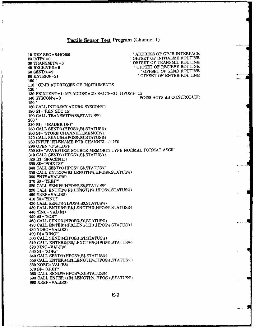
Tactile Sensor Test Program (Channel 1)
10 DEF SEG=&HC400 'ADDRESS OF GP-IB INTERFACE20 INIT%=0 'OFFSET OF INITIALIZE ROUTINE30 TRANSMIT% =3 'OFFSET OF TRANSMIT ROUTINE40 RECEIVE% = 6 'OFFSET OF RECIEVE ROUTINE50 SEND%= 9 ' OFFSET OF SEND ROUTINE60 ENTER%=21 'OFFSET OF ENTER ROUTINE100'110 ' GP-IB ADDRESSES OF INSTRUMENTS120'130 PRINTER%= 1: MY.ADDR%= 21: K617% =27: HPOS% 15140 SYSCON%=0 'PC488 ACTS AS CONTROLLER150'160 CALL INIT%(MY.ADDR%,SYSCON%)180 S$="REN SDC 15"190 CALL TRANSMIT%(S$,STATUS%)200'220 S$- 1EADER OFF"250 CALL SEND%(HPOS%,S$,STATUS%)260 S$="STORE CHANNEL1,MEMORY1"270 CALL SEND%(HPOS%,S$,STATUS%)280 INPUT "FILENAME FOR CHANNEL 1";DF$290 OPEN "0",#1,DF$300 S$="WAVEFORM SOURCE MEMORY1 TYPE NORMAL FORMAT ASCII310 CALL SEND%(HPOS%,S$,STATUS%)320 R$=SPACE$(15)330 S$ ="POINTS?"340 CALL SEND%(HPOS%,S$,STATUS%)350 CALL ENTER%(R$,LENGTH%,HPOS%,STATUS%)360 PNTS=VAL(R$)370 S$="YREF?"380 CALL SEND%(HPOS%,S$,STATUS%)390 CALL ENTER%(R$,LENGTH%,HPOS%,STATUS%)400 YREF=VAL(R$)410 S$='YINC?"420 CALL SEND%(HPOS%,S$,STATUS%)430 CALL ENTER%(R$,LENGTH%,HPOS%,STATUS%)440 YINC = VAL(R$)450 S$ = '"YORT460 CALL SEND%(HPOS%,S$,STATUS%)470 CALL ENTER%(R$,LENGTH%,HPOS%,STATUS%)480 YORG=VAL(R$)490 S$ ="XINC?"500 CALL SEND%(HPOS%,S$,STATUS%)510 CALL ENTER%(R$,LENGTH%,HPOS%,STATUS%)520 XINC=VAL(R$)530 S$="XOR?"540 CALL SEND%(HPOS%,S$,STATUS%)550 CALL ENTER%(R$,LENGTH%,HPOS%,STATUS%)560 XORG=VAL(R$)570 S$ ="XREF?"580 CALL SEND%(HPOS%,S$,STATUS%)590 CALL ENTER%(R$,LENGTH%,HPOS%,STATUS%)600 XREF=VAL(R$)
E-3

610 S$ ="DATA?"620 CALL SEND%(HPOS%,S$,STATUS%)630 S$="MLA TALK 15"640 CALL TRANSMIT%(S$,STATIJS%)650 X$ =SPACE$(15)660 Y$=SPACE$( 15)670 FOR 1= I TO PNTS680 CALL RECEIVE%(Y$,LENGTH%,STATUS%)690 X=(I*XINC)+XORG700 Yt=((VAL(Y$)-YREF)*YINC) +YORG710 WRITE #1,X,Y720 NEXT I730 CLOSE #1740 S$="LISTEN 15 MTA"750 CALL TRANSMIT%(S$,STATUS%)760 S$ = "LOCAL"770 CALL SEND%(HPOS%,S$,STATUS%)780 SYSTEM
E-4

Tactile Sensor Test Program (Channel 2)
10 DEF SEG=&HC400 'ADDRESS OF GP-IB INTERFACE20 INIT%=0 'OFFSET OF INITIALIZE ROUTINE30 TRANSMIT%=3 'OFFSET OF TRANSMIT ROUTINE40 RECEIVE%=6 'OFFSET OF RECIEVE ROUTINE50 SEND%=9 'OFFSET OF SEND ROUTINE60 ENTER%=21 'OFFSET OF ENTER ROUTINE100'110 'GP-IB ADDRESSES OF INSTRUMENTS120'130 PRINTER%= 1: MY.ADDR% = 21: K617%=27: HPOS% 15140 SYSCON%= 0 'PC488 ACTS AS CONTROLLER150'160 CALL INIT%(MY.ADDR%,SYSCON%)180 S$="REN SDC 15"190 CALL TRANSMIT%(S$,STATUS%)200'220 S$="HEADER OFF"250 CALL SEND%(HPOS%,S$,STATUS%)260 S$="STORE CHANNEL2,MEMORY2'270 CALL SEND%(HPOS%,S$,STATUS%)280 INPUT "FILENAME FOR CHANNEL 2";DF$290 OPEN "O",#1,DF$300 S$='WAVEFORM SOURCE MEMORY2 TYPE NORMAL FORMAT ASCII"310 CALL SEND%(HPOS%,S$,STATUS%)320 R$=SPACE$(15)330 S$= "POINTS?"340 CALL SEND%(HPOS%,S$,STATUS%)350 CALL ENTER%(R$,LENGTH%,HPOS%,STATUS%)360 PNTS=VAL(R$)370 S$='YREF?"380 CALL SEND%(HPOS%,S$,STATUS%)390 CALL ENTER%(R$,LENGTH%,HPOS%,STATUS%)400 YREF = VAL(R$)410 S$="YINC?"420 CALL SEND%(HPOS%,S$,STATUS%)430 CALL ENTER%(R$,LENGTH%,HPOS%,STATUS%)440 YINC=VAL(R$)450 S$ = "YOR?"460 CALL SEND%(HPOS%,S$,STATUS%)470 CALL ENI .- -...- ' T NGTH%,HPOS%,STATUS%)480 YORG= VAL(R$)490 S$ = "XINC?"500 CALL SEND%(HPOS%,S$,STATUS%)510 CALL ENTER%(R$,LENGTH%,HPOS%,STATUS%)520 XINC=VAL(R$)530 S$ ="XOR?"540 CALL SEND%(HPOS%,S$,STATUS%')550 CALL ENTER%(R$,LENGTH%,HPOS%,STATUS%)560 XORG= VAL(R$)570 S$ ="XREF?"580 CALL SEND%(HPOS%,S$,STATUS%)590 CALL ENTER%(R$,LENGTH%,HPOS%,STATUS%)600 XREF=VAL(R$)
E-5

610 S$="DATA?"620 CALL SEND%(HPOS%,S$,STATUS%)630 S$="MLA TALK 15"
* 640 CALL TRANSMIT%(S$,STATUS%)650 X$=SPACE$(15)660 Y$ =SPACE$(15)670 FOR I= 1 TO PNTS680 CALL RECEIVE%(Y$,LENGTH%,STATUS%)690 X=(I*XJNC)+XORG700 Y= ((VAL(Y$)-YREF)*YINC) +YORG
*710 WRITE #1,X,Y720 NEXT I730 CLOSE #1740 S$ ="LISTEN 15 MTA750 CALL TRANSMIT%(S$,STATUS%)I760 S$ = "LOCAL"
* 770 CALL SEND%(HPOS%,S$,STATUS%)780 SYSTEM
E-6

Bias Voltage Response Program
10 DEF SEG=&HC40020 INIT% = 0:TRANSMIT% = 3:RECEIVE% = 630 SEND% = 9:SPOLL% = 12:ENTER% = 2140 MY.ADDR% = 21:K617% = 27:SYSCON% = 0 'Instrument Addresses60 CALL INIT%(MY.ADDR%,SYSCON%)70 S$="REN SDC 27"80 CALL TRANSMIT%(S$,STATUS%)90 '****SET-UP ELECTROMETER FOR MEASUREMENT100 VSET$="0"110 S$="FOX" 'SET TO MEASURE VOLTS120 CALL SEND%(K617%,S$,STATUS%)130 S$ ="DOX"140 CALL SEND%(K617%,S$,STATUS%)150 REM INPUT "NAME OF DATA FILE?", DFILE$160 DFILE$ ="rlbvlt.dat"
170 OPEN "O",#1,DFILE$180 FLAG= 0190 REM INPUT "ZEROING ELECTROMETER, HIT RETURN WHEN READY", NULL$200 S$="ClXZIXCOX"210 CALL SEND%(K617%,S$,STATUS%)220 REM INPUT "HIT RETURN TO BEGIN TEST RUN", NULL$230 S$="O1Q7X"240 CALL SEND%(K617%,S$,STATUS%)250 S$="GlX"260 CALL SEND%(K617%,S$,STATUS%)270 RT=O280 VRD$ = SPACE$(12)290'300 'BEGIN DATA LOOP310 T=0320 TMR2 = TIMER330 WHILE ABS(TIMER-TMR2) < 25:WEND340 CALL ENTER%(VRD$,LENG%,K617%,STATUS%)350 T=T+25360 RT=RT+25370 VRD=VAL(VRD$)380 PRINT RT,VRD390 WRITE #1,RT,VRD400 CLOSE #1410 OPEN DFILE$ FOR APPEND AS #1420 '430 GOTO 310440'450 CLOSE #1460 SYSTEM
E-7
A

.. ... i iI I I !.
Group Test Program
10 DEF SEG=&HC400 'ADDRESS OF GP-IB INTERFACE20 INIT%= 0 'OFFSET OF INITIALIZE ROUTINE30 TRANSMIT%=3 'OFFSET OF TRANSMIT ROUTINE40 RECEIVE%=6 'OFFSET OF RECIEVE ROUTINE50 SEND%=9 'OFFSET OF SEND ROUTINE
• 60 SPOLL%= 12 'OFFSET OF SERIAL POLL ROUTINE70 ENTER%-21 'OFFSET OF ENTER ROUTINE100 'GP-IB ADDRESSES OF INSTRUMENTS110 PRINTER%=1: MY.ADDR%=21: K617%=27120 BK2032% = 6130'140 SYSCON%=0 'PC488 ACTS AS CONTROLLER150'160 CALL INIT%(MY.ADDR%,SYSCON%)180 S$="REN SDC 27"190 CALL TRANSMIT%(S$,STATUS%)200 'SET-UP ELECTROMETER FOR MEASUREMENT220 S$="FOX" 'SET TO MEASURE VOLTS230 CALL SEND%(K617%,S$,STATUS%)270 INPUT "NAME OF DATA FILE?", DFILE$280 OPEN "O",#1,DFILE$290 INPUT "ZEROING ELECTROMETER, HIT RETURN WHEN READY', NULL$300 S$="CIXZlXCOX"310 CALL SEND%(K617%,S$,STATUS%)320 INPUT "HIT RETURN TO BEGIN TEST RUN", NULL$330 S$ ="Q7X"340 CALL SEND%(K617%,S$,STATUS%)350 S$="G1X"360 CALL SEND%(K617%,S$,STATUS%)370 VRD$=SPACE$(12)380 FOR ELC = 1 TO 25390 READ PN400 PRINT"HIT RETURN TO READ PIN";PN410 INPUT NULL$420 CALL ENTER%(VRD$,LENG%,K617%,STATUS%)430 VRD=VAL(VRD$)440 READ XV,YV450 PRINT XV,YV,VRD460 WRITE #1,XV,YV,VRD470 NEXT ELC480 CLOSE #1490 DATA 10,1,1,11,1,2,12,2,1,13,2,2,14,2,3,15,3,1500 DATA 16,3,2,17,4,1,18,4,2,19,4,3,20,5,1,21,5,2,22,5,3510 DATA 43,5,4,44,5,5,45,4,4,46,4,5,47,3,3,48,3,4,49,3,5520 DATA 50,2,4,51,2,5,52,1,3,53,1,4,54,1,5
E-8

Appendix F: Tactile Sensor Test Data
2 M n-
TR -i k D 7 r
5 R- -1 1• --, I
-C 5 -K ~ -0 1 j. -
T.-
Figure F-1. 25R m Thick PVDF Film With a 0.8g Load.
0
I I-H I- 1-1-- - ....--1 -1 --
-2 -2 2' 3 I 23I 00 0 ' 0 j ./
;II i
L!-T i
Figure F-2. 25pRm Thick PVDF Film With a 14.5g Load.
F-1
* -,---=, -4- L mm mmm ll~~l m - ±m

F r F. 2 - t DF lm Wit dI 1 1 ,1i ' I ' I
* 6T-1
K ' I tHI L- I : '| I -----
-L -Z 3 Z; 5 _
Figure F-4. 25km Thick PVDF Film With a 37g Load.
, , ! *F - ,a'
i iI - IT 2 ' !,L h1JI ,
, 4+ 1-1
I I ' ' ' I I ,
-,,-+,--, ,-k-4-,- , a - - 4 :
Figure F-4. 25pxm Thick PVDF Film With a 37g Load.
F-2

25 M icrorn Tn/ (i -" '% F. i
-Z)s -0 3 -0 i 0 i o 3 0 c C. 9 1 ? I I
Figure F-5. 25 Lm Thick PVDF Film With a 61g Load.
2 M, Lrc, n T 4-,- , i 4
-- -77 -
3C..
Figure F-6. 25 tm Thick PVDF Film With a 76g Load.
F-3
3 _ _ - _
" i 2 -I I np I -I - , -...

4J M V r:,r- Tr cLS PrE W t
I I 7 I I I . •
S°r -- - '- r - - ... - -1 --
XKI , -- , i-,, ,
Li4F4
Figure F-7. 4O tm Thick PVDF Film With a 0.8g Load.
I If
Figure F-8. 40m Thick PVDF Film With a 14.5g Load.
F-4
0

40 M i cron ) ci T-IL. FS,- Q4ur's ,t; 21 :c u
6 - - I - t - -,.. m
S 7-
- 5 - 3 -0 0 C0 3 1 CfI 1 _ 1
Figure F-9. 40tm Thick PVDF Film With a 21g Load.
4- M '.'', : ""j
F rn! .-- P- w # tJ h a 3 tg _- 1
.. . .. _ ... .--- _
i~1 I-r 77
4- 4 -
C K1 4 1 Z) 5
Figure F-10. 4 0ptm Thick PVDF Film With a 37g Load.
F-5

. I. , ii I .. . ...I I I I I 11 1 I [. , ,, m m it i
0: Micror T. Ick -VDF F
5" Al- W t a F,19 08
o8 - .4---- -- -- - I--1-i ,f-' ° .. .. .~~- -T ' --- - + -i -
SI I I
S -01 -0 1 0 1 0 9 1-
I3 -
Te (Seconds;
Figure F-11. 40pm Thick PVDF Film With a 61g Load.
4 _ MiCr-o- T ick F-vDF F
1 '2 3,n w 5 a0 .080
T i 11J--§
Figre F-12. 40pLm Thick PVDF Film With a 76g Load.
F-6

52 Micr-on Tn ,rk c VDk FI m5, P t' a 0 6g
10 -4 i.--.----
T=T
-05 -0 3 -0 1 C 05 0 0 9 11 13
Figure F-13. 521im Thick PVDF Fi!m With a 0.8g Load.
52 Micron T k ",- F, Im
8 i - - .. ... .- -: ' - -i
'K-4---
8T- _LT- - ,
-0 -0 - 3 -0 1 -,) 1 0 3 C -, Q 0 1 1 3
Figure F-14. 52Am Thick PVDF Film With a 14.5g Load.
F-7

52Mrm 7~c 71tw
s iurs F t Thic g .D F W
-IfIIr-. - - ,-- j I-)9 . . . .... ....9
-- - -- ek I _
1-- - - - - I--~ -- -i
1-* Seots
Figure F-15. 52xm Thick PVDF Film With a 21g Load.
S, >'S * IrF a 3g LOad
I; __ _
5 -
-, ~--1-111
Figure F-16. 52pm Thick PVDF Film With a 37g Load.
F-8

5- P-fl d, a 6-Y
II I?~ 7 1VI
-7I- ' - - I
- - 4 -
3 T- 7 iFigure F-17. 521Rm Thick PVDF Film With a 61g Load.
.... . .. ... F - -- -
._Kl~$Th t--t----
Figure F-18. 52p.m Thick PVDF Film With a 76g Load.
F-9

110 Micron TnliCK PVDF Film C2V BiaseodS. Rri- *Itm a 0 Gg Lad
30
-0 3 -0 3 - 0 0 3 3 7 a
Orme S eccf,: , -
Figure F-19. 11Om Thick PVDF Film With a 0.8g Load.
i M .-- - T-,c< 'VE F B E
T1 .....7 -N7-7
6 - -~---t -- --t-- 1 -.-- --- .
I I
I-a-I - e.- r-,
Figure F-20. 10 1m Thick PVDF Film With a 14.5g Load.
F-10

4---
-t 4- t, -4 -
M ~W~<~~
Figure F-22. 11O Lm Thick PVDF Film With a 37g Load.
F-1

NA MC -) 7 rCK V v B-~S .P-n E'g at
SIII I I II -2
-..
* I--- - + - - -------- ---.-
I ' i 'I , :
Figure F-23. 1101m Thick PVDF Film With a 61g Load.
-. . -. 4 - - 4
Figure F-24. 1ll1m Thick PVDF Film With a 76g Load.
F-12

Bibliography
1. Pennywitt Kirk E. "Robotic Tactile Sensing," Byte, 11: 177-200 (January1986).
2. Barth, Philip W. "Sensor Applications in Robotics," Robotics Engineering: 17-20 (September 1986).
3. Chatigny, J. Victor and Lester E. Robb. "Piezo Film Sensors," Sensors: 50-55 (May 1986).
4. Dario, P. and D. De Rossi. "Tactile Sensors and the Gripping Challenge,"IEEE Spectrum: 46-52 (August 1985).
5. McAlpine, George A. "Tactile Sensing," Sensors: 7-16 (April 1986).
6. Dario, P. and others. "Ferroelectric Polymer Tactile Sensors for Prostheses,"Ferroelectrics, 60: 199-214 (1984).
7. Pirolo, Capt David G. Piezoelectric Polymer Tactile Sensor Arrays forRobotics. M.S. Thesis, AFIT/GE/ENG/87D-52. School of Engineering, AirForce Institute of Technology (AU), Wright-Patterson AFB OH, December1987.
8. Osterhout, John K. "Magic: A VLSI Layout Editor," 1986 Berkeley CADTools User's Manual. Berkeley, (1986).
9. Mason, Warren P. Piezoelectric Crystals and Their Application toUltrasonics. New York: D. Van Nostrand Company, Inc., 1950.
10. Cady, Walter G. Piezoelectricity, An Introduction to the Theory andApplications of Electromechanical Phenomena, Volumes I and II. New York:Dover Publications, Inc., 1964.
11. KYNAR Piezo Film Department. Kynar Piezo Film Technical Manual.Pennwalt Corporation, King of Prussia PA, 1987.
12. KYNAR Piezo Film Department. Kynar Piezo Film Technical Manual.Manual 10-M-11-83-M. Pennwalt Corporation, King of Prussia PA, 1983.
13. Kraus, John D. Electromagnetics (Third Edition). New York: McGraw-Hill,1984.
14. van der Ziel, Aldert. Solid State Physical Electronics (Second Edition).Englewood Cliffs: Prentice-Hall, 1968.
BIB-1

15.Jaffe, Bernard and others. Piezoelectric Ceramics. New York: AcademicPress, 1971.
16. Kawai, Heiji. 'The Piezoelectricity of Poly (vinylidene Fluoride)," JapanJournal of Applied Physics, 8: 975-976 (May 1969).
17. KYNAR Piezo Film Department. Appendix A, Human Tactile Capabilities.Pennwalt Corporation, King of Prussia PA, 1984.
18. Weste, Neil and Kamran Eshraghian. Principles of CMOS VLSI Design ASystems Perspective. Reading MA: Addison-Wesley Publishing Company,1985.
0 19. Tuinenga, Paul W. SPICE: A Guide to Circuit Simulation & Analysis UsingPSpice. Englewood Cliffs NJ: Prentice-Hall, Inc., 1988.
20. Millman, Jacob. Microelectronics. New York: McGraw-Hill Book Company,1979.
21. Solvay & Cie. Solef Piezo Film Principal Properties. Experimental ProductData Sheet. Solvay & Cie, Brussels, Belgium, 1987.
22. KYNAR Piezo Group. Kynar Piezo Film. TR-3M-8-86-PF1O1. PennwaltCorporation, King of Prussia PA, undated.
23. KYNAR Plastics Department. Kynar polwinylidene Fluoride ChemicalResistance Chart. 25-M-8-85-TR. Pennwalt Corporation, King of Prussia PA,undated.
0
tt
V|
'I
BIB-2

Vita
Captain Rocky R. Reston was born on
He graduated from Air Academy High School, Colorado Springs,
Colorado in 1980, and immediately entered the United States Air Force
Academy where he graduated in 1984 with a Bachelor of Science in Electrical
Engineering and a commission in the United States Air Force. Upon
graduation, he was assigned to the Radar Test Facility of the 4 4 84th Test
Squadron, Tyndall Air Force Base, Florida as an instrumentation engineer. In
May of 1987, he entered the School of Engineering, Air Force Institute of
Technology.
VIT-1
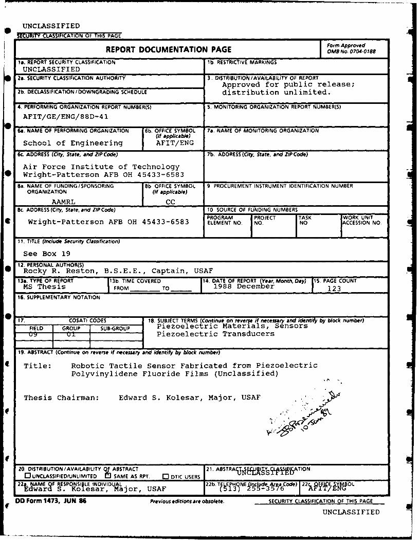
UNCLASSIFIEDSECURITY CLASSIFICATION OF THIS PAGE
Form ApprovedREPORT DOCUMENTATION PAGE OMB No. 0704-0188
la. REPORT SECURITY CLASSIFICATION lb. RESTRICTIVE MARKINGSUNCLASSIFIED
2a. SECURITY CLASSIFICATION AUTHORITY 3. DISTRIBUTION /AVAILABILITY OF REPORTApproved for public release;
2b. DECLASSIFICATION /DOWNGRADING SCHEDULE distribution unlimited.
4. PERFORMING ORGANIZATION REPORT NUMBER(S) 5. MONITORING ORGANIZATION REPORT NUMBER(S)
AFIT/GE/ENG/88D-41
6a. NAME OF PERFORMING ORGANIZATION 6b. OFFICE SYMBOL 7a. NAME OF MONITORING ORGANIZATION(If applicable)
School of Engineering AFIT/ENG
6c. ADDRESS (City, State, and ZIP Code) 7b. ADDRESS (City, State, and ZIP Code)
Air Force Institute of TechnologyWright-Patterson AFB OH 45433-6583
Sa. NAME OF FUNDING/SPONSORING 8b OFFICE SYMBOL 9 PROCUREMENT INSTRUMENT IDENTIFICATION NUMBER
ORGANIZATION (If applicable)
AAMRL CCSc. ADDRESS (City, State, and ZIP Code) 10 SOURCE OF FUNDING NUMBERS
PROGRAM PROJECT TASK WORK UNITWright-Patterson AFB OH 45433-6583 ELEMENT NO. NO. NO ACCESSION NO.
11. TITLE (Include Security Classification)
See Box 19
12. PERSONAL AUTHOR(S)Rocky R. Reston, B.S.E.E., Captain, USAF
13a. TYPE OF REPORT 113b. TIME COVERED 14. DATE OF REPORT (Year, Month, Day) 15. PAGE COUNTMS Thesis I FROM TO 1988 December . 123
16. SUPPLEMENTARY NOTATION
17. COSATI CODES 18. SUBJECT TERMS (Continue on reverfe if necessary and identify by block number)
FIELD GROUP SUB-GROUP Piezoelectric Materials, Sensors09 _1 I Piezoelectric Transducers
19. ABSTRACT (Continue on reverse if necessary and identify by block number)
Title: Robotic Tactile Sensor Fabricated from PiezoelectricPolyvinylidene Fluoride Films (Unclassified)
Thesis Chairman: Edward S. Kolesar, Major, USAF
20. DISTRIBUTION /AVAILABILITY ABSTRACT 21. ABSTRACJgJdI{ ty5ATIONr UNCLASSIFIED/UNLIMITED 0 SAME AS RPT. 3 DTIC USERS
22a. NAME OF RESPONSIBLE INDIVIDUAL 22b. TEEPHNE41qrtd oe3 racode) 22c1 ,JE .Y4OLEdward S. Kolesar, Major, USAF
DD Form 1473, JUN 86 Previous editions are obsolete. SECURITY CLASSIFICATION OF THIS PAGE
UNCLASSIFIED

UNCLASSIFIEDSECURITY CLASSIFICATIN OF THIS PAGE
(C on t i/ed from Block 19)
The purpose of this research effort was to design,
fabricate and test a robotic tactile sensor fabricated from
polyvinylidene fluoride (PVDF) films coupled to a silicon
substrate containing active amplification circuitry. The
integrated circuit incorporated 25 sensor electrode pads
(0.6mmxO.6mm each) arrayed in a 5x5 grid with a spacing of
0.6mm between electrodes (this corresponds to a spatial
resolution four times greater than the human fingertip). The
on-board amplification circuitry consisted of a dual MOSFET
amplifier (with a gain of 5) for each sensor electrode.
Four different sensor configurations were fabricated and
tested. The configurations varied only in the thickness of
the PVDF film used (25 microns, 40 microns, 52 microns, and
110 microns). The individual elements of each of the sensor
configurations were tested and the sensor based on the 25
micron thick film was considered the optimal sensor of the
four. This decision was based on its superior biasing ability
and its inear operation over the test loading range (0.8g toande
76g). Addiionally, there was essentially no coupling between
nearest neighbors for all of the sensor configurations. A
group loading test (where multiple elements were loaded) was
also performed, but problems with obtaining a consistent no-
load output across the ertire array prevented a true picture
of the performance of the sensor. Methods for improving the
tactile sensor (including a means for obtaining a consistent
no-load output across the entire array) are discussed in the
final chapter.
UNCLASSIFIEDSE&TRITY CLASSIFICATION OF THIS PAGE