i-fuse™: a disruptive otp technology · device trimming / calibration (eliminate eeprom) mcu code...
TRANSCRIPT

Attopsemi Technology, May 13, 2019 1
I-fuse™: A Disruptive OTP Technology
Jeffrey Lin/Shine Chung
May 5, 2019
Attopsemi Technology
1A2-A1 No. 1 Li-Hsin 1st Rd, Hsinchu, Taiwan 300-78
886+(3)666-3150x211, 886+920-566-218
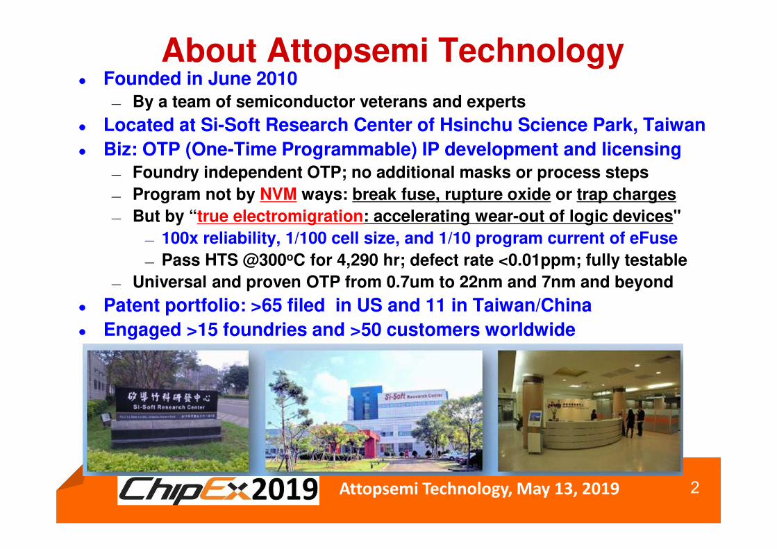
Attopsemi Technology, May 13, 2019 2
About Attopsemi Technology Founded in June 2010
— By a team of semiconductor veterans and experts
Located at Si-Soft Research Center of Hsinchu Science Park, Taiwan
Biz: OTP (One-Time Programmable) IP development and licensing— Foundry independent OTP; no additional masks or process steps
— Program not by NVM ways: break fuse, rupture oxide or trap charges
— But by “true electromigration: accelerating wear-out of logic devices"
— 100x reliability, 1/100 cell size, and 1/10 program current of eFuse
— Pass HTS @300oC for 4,290 hr; defect rate <0.01ppm; fully testable
— Universal and proven OTP from 0.7um to 22nm and 7nm and beyond
Patent portfolio: >65 filed in US and 11 in Taiwan/China
Engaged >15 foundries and >50 customers worldwide

Attopsemi Technology, May 13, 2019 3
Different OTP TechnologiesStore data Permanently but Program Once
NVM device
Other OTP: NVM mechanismsBreak fuse, Rupture oxide, or trap charges in floating gates
Other OTP: NVM ProblemsLarge size, HV PGM, charge pumps, hard to use, low reliability
Revolutionary I-fuse™: true logic device OTP to win
Floating-gateOxide rupture
eFuse
Non-break fuse Break fuse Rupture oxide Trap charges
≦0.6um ≦0.18um ≦ 0.18um, ≧14nm ≧0.35um, ≦ 0.6um
Deterministic Explosive Explosive Statistical
No problem Grow back Self-healed data retention
<0.01ppm defect 29ppm defect 10ppm defect 100ppm defect
I-fuse™

Attopsemi Technology, May 13, 2019 4
B_Fuse
0.00E+00
1.00E-03
2.00E-03
3.00E-03
4.00E-03
5.00E-03
6.00E-03
7.00E-03
8.00E-03
0 0.2 0.4 0.6 0.8 1 1.2 1.4 1.6 1.8 2
V
I(A)
B_03
B_04
B_05
Critical current: Onset of Thermal run away (QGEN > QLOSS)
(UD50SP)
eFuse
(d)
Power devices should not operate in thermal runaway. So programming a fuse should not.
I-fuse™: non-explosive fuse; Guaranteed reliable by physics
eFuse: explosive fuse => create debris => grow back
Electromigration
threshold
I-fuse eFuse
(c)
(d)
(XH018)
V
Break point: Onset of Thermal runaway (QGEN > QLOSS)
I-Fuse™ vs. eFuse Programming
I-fuse™
(c)

Attopsemi Technology, May 13, 2019 5
I-Fuse™: ProgrammingeFuse: apply voltage to spec; generate a high current to blow eFuses
I-fuse™: has a natural program window
Program window can be adjust by cell size, I-fuse™ structure, etc.
I-fuse™ program window characterization
Start with a very low voltage to PGM I-fuse™
Increment PGM voltage until all bits can be PGM’d—Low Bound (LB)
Increment PGM after LB until read failure--- exceeding High Bound (HB)
Set the typical PGM voltage as average of LB and HB
PGM yield can be estimated from the program defect curve

Attopsemi Technology, May 13, 2019 6
Un-Programmed PGM below LB• Before program, W is
uniformly distributed• Insufficient PGM: some W got
insufficiently migrated
Si
W W
Si
TEM/EDX of I-fuse™ on WSi2 (1/2)

Attopsemi Technology, May 13, 2019 7
I-fuse™ PGM PGM over HB• After program, W migrated
to anode; Si intact• Si got severely damaged, W
scattered around
Si
W W
Si
TEM/EDX of I-fuse™ on WSi2 (2/2)
Attopsemi Technology, May 13, 2019 8
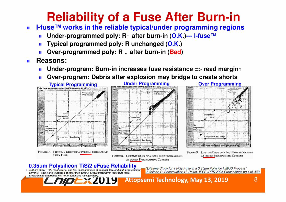
Reliability of a Fuse After Burn-inI-fuse™ works in the reliable typical/under programming regions
Under-programmed poly: R↑ after burn-in (O.K.)--- I-fuse™
Typical programmed poly: R unchanged (O.K.)
Over-programmed poly: R ↓ after burn-in (Bad)
Reasons:Under-program: Burn-in increases fuse resistance => read margin↑Over-program: Debris after explosion may bridge to create shortsTypical Programming
0.35um Polysilicon TiSi2 eFuse Reliability
Under Programming Over Programming

Attopsemi Technology, May 13, 2019 9Attopsemi ConfidentialAttopsemi Confidential
I-Fuse™ Passed 150oC HTOL, 2Khr I-fuse™ passed HTOL 150oC, 2,000hr to AEC-Q100 Grade 0 qual
— Cell current distributions for pre-/post PGM cells are narrow
— Separation between pre-/post PGM cells are far apart
Cell current variation after stress vs. before stress (32Kb)— Pre-PGM cell currents decreased --- additional annealing for fuse
— Post-PGM cell currents virtually didn’t changed
Cell current before HTOLCe
ll c
urr
en
t a
fte
r 2
Kh
r H
TO
L
Cell current before & after
Cu
mu
late
d p
erc
en
tag
eProgram bits
Un-program bits
Attopsemi Technology, May 13, 2019 10
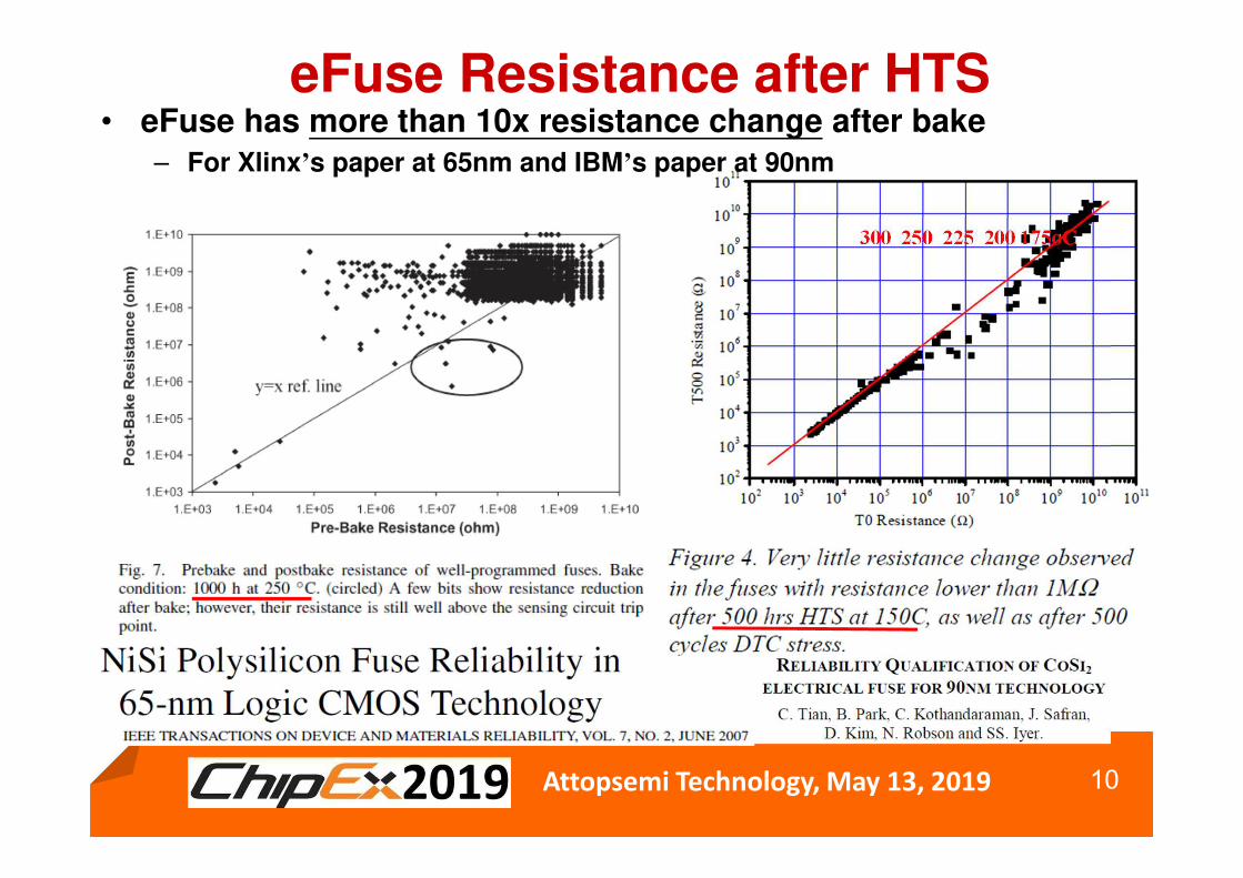
eFuse Resistance after HTS • eFuse has more than 10x resistance change after bake
– For Xlinx’s paper at 65nm and IBM’s paper at 90nm
300 250 225 200 175oC

Attopsemi Technology, May 13, 2019 11Attopsemi Confidential
I-Fuse™: ZERO DefectField return is very costly
10x costs from wafer sort, packaged chip, module, PCB, to system
ZERO defect after shipping
Defects should be found out and screened before shipping
I-fuse™ can achieve ZERO defect
OTP dilemma: fully tested before shipping; but can’t be used any more
Guarantee cell programmable: if initial fuse resistance <400Ω
Guarantee 100% programmable: if programmed within specs
Fully testable*: every functional block, including program circuits
Create non-destructive program state to read 1 for complex tests
Concurrent low-voltage PGM and read same cell => fake reading 1
$0.1 $1 $10 $100 $1000

Attopsemi Technology, May 13, 2019 12
Conclusion: Non-Explosive I-Fuse™Low Program Voltage & Current
Small size
No charge pump
PGM voltage about core or I/O voltage
Short program time
Deterministic programming behavior
Narrow resistance distribution
Easy to use (No HV device/circuit)
High reliability
High temperature
High data security
Fully testability
Applications: AI, IoT, Automotive, Industrial, communication
The only OTP programming mechanism can be modeled by physics: heat generation/dissipation and electro-migration

Attopsemi Technology, May 13, 2019 13
BACKUP

Attopsemi Technology, May 13, 2019 14
OTP Applications
Memory redundancy (replace laser fuse)
Chip ID, Security Key, IoT
Device trimming / calibration (eliminate EEPROM)
MCU code storage (replace flash)
Product feature selection
OTP (One-Time-Programmable): a memory IP be programmableonly once to store permanent dataOTP allows each IC to be customized after fabrication
Every chip needs OTP, if available, affordable, & reliable
3D IC repair

Attopsemi Technology, May 13, 2019 15
Electro-migration
Rupture
Melt
Debris
Defect: 1E-5 (IBM)
E-fuse
Soft breakdown
Hard breakdown
Gate oxide Breakdown
IEDM 97-73
Logic EPROM
e-
e-
70A: 0.35um MOS
•Only good for 0.35/0.5um CMOS
• Data retention

Attopsemi Technology, May 13, 2019 16
Efuse vs. I-Fuse™
28nm and beyond eFuse* I-fuse™
Program current Up to 100mA <3mA
HTS qual 4Kb passed 125oC 1Khr with 2 cells per bit
256Kb passed 250oC 1Khr without any redundancy
Read time in life < 1sec Unlimited read time
Program yield A few % loss ~100%
Scalability NO YES
Testability NO YES. Achieve ZERO defect
Revolutionary I-fuse™ fixes all problems in eFuse
Reliability & qualification guaranteed by physics
Robust OTP technologies NOT to cause any problems
* Customers testimonies

Attopsemi Technology, May 13, 2019 17
Beyond 28nm: I-Fuse™ vs. Anti-Fuse(AF)
Fuse current programming prevails AF voltage programming !!! Non-explosive I-fuse™ prevails explosive eFuse !!!
Narrower fuse => low PGM current
Low PGM current => low PGM volt.
I-fuse™ scalable to 14/7/5/3/2/1nm
Non-breaking I-fuse wins breaking
I-fuse™: current PGMBVJ/BVO: Breakdown voltage of junction/oxide
VPP~BVO
Tox
BVj
Supply voltages lower and lower
Oxide/PGM voltage can’t scaled
Junction breakdown before oxide
AF Hard to work beyond 14/16nm
Anti-fuse: voltage PGM
Icrit
0
0.002
0.004
0.006
0.008
0.01
0.012
0.014
0.016
0.018
0.02
0.022
0.024
0 50 100 150 200 250 300 350 400 450 500
Lg
WSi
TiSi
NiSi
CoSi
WSi
HKMG
PGM current (A)
Nodes (nm)

Attopsemi Technology, May 13, 2019 18
• Founder: Shine Chung• Harvard graduate in Applied Physics• 30 years of IC design experience• Memory design in AMD, Intel, and HP• PA-WW architect (PA-WW: precedent of Intel’s Merced)• Director at TSMC (eFuse pioneer)• VLSI and ISSCC technical committee for 4 years• Two-time TSMC innovation award recipient• 61 patents granted before Attopsemi• Filed >65 U.S. patents and 54 granted after Attopsemi
The Team
• Co-founder & VP of Eng: WK Fang• MSEE from Ann Harbor, U. of Michigan• 20-year experiences in memory • Technical Manager at TSMC• Department Mgr for eFuse• Design managers for N90/N65 SRAM TV, eDRAM• MTS in SRAM, FIFO, CAM at IDT

Attopsemi Technology, May 13, 2019 19
BACKUP