hyppi noc: bringing hybrid plasmonics to an opto
TRANSCRIPT

HyPPI NoC: Bringing Hybrid Plasmonics to an Opto-Electronic Network-on-Chip
Vikram K. Narayana, Shuai Sun, Armin Mehrabian, Volker J. Sorger, and Tarek El-GhazawiDepartment of Electrical and Computer Engineering
The George Washington UniversityWashington, D.C. 20052
{vikram,sunshuai,armin,sorger,tarek}@gwu.edu
Abstract—As we move towards an era of hundreds of cores,the research community has witnessed the emergence of opto-electronic network on-chip designs based on nanophotonics, inorder to achieve higher network throughput, lower latencies,and lower dynamic power. However, traditional nanophotonicsoptions face limitations such as large device footprints com-pared with electronics, higher static power due to continuouslaser operation, and an upper limit on achievable data rates dueto large device capacitances. Nanoplasmonics is an emergingtechnology that has the potential for providing transformativegains on multiple metrics due to its potential to increasethe light-matter interaction. In this paper, we propose andanalyze a hybrid opto-electric NoC that incorporates Hy-brid Plasmonics Photonics Interconnect (HyPPI), an opticalinterconnect that combines photonics with plasmonics. Weexplore various opto-electronic network hybridization optionsby augmenting a mesh network with HyPPI links, and comparethem with the equivalent options afforded by conventionalnanophotonics as well as pure electronics. Our design spaceexploration indicates that augmenting an electronic NoC withHyPPI gives a performance to cost ratio improvement of upto 1.8×. To further validate our estimates, we conduct tracebased simulations using the NAS Parallel Benchmark suite.These benchmarks show latency improvements up to 1.64×,with negligible energy increase. We then further carry outperformance and cost projections for fully optical NoCs, usingHyPPI as well as conventional nanophotonics. These futuristicprojections indicate that all-HyPPI NoCs would be two ordersmore energy efficient than electronics, and two orders morearea efficient than all-photonic NoCs.
Keywords-Hybrid Plasmon-Photonics; Network-on-Chip;Hybrid NoC;
I. INTRODUCTION AND MOTIVATION
With the drive towards an increasing number of coresover the past decade, the field has witnessed network-on-chip (NoC) architectures becoming mainstream in high-performance computing and embedded processors. However,challenges arising from the steadily rising memory demandsof applications, as well as the rising power budget for on-chip networks, has led researchers to actively investigatenanophotonics-based opto-electronic networks [1].
Photonic interconnects have been considered as a pro-mising on-chip option in the ITRS roadmap since the mid-2000s. Because of the parallelism of bosons, it is ableto support Wavelength Division Multiplexing (WDM) fora higher bandwidth compared to electrical interconnects.
Furthermore, the low optical attenuation of photonics en-ables on-chip communications with small energy lossesduring light propagation. Photonics is thus efficient forpassive operations such as data transmission. Examples ofproposed photonic NoCs include: Corona [2], a NoC withmulti-write single-read optical loops accessed through token-based arbitration; LumiNoC, a NoC with multiple opticalsubnets [3]; Flexishare [4], a multi-stage optical crossbarinterconnect; and ATAC, a hybrid NoC that uses an opticalloop for broadcast operations [5].
While nanophotonics has proven to be promising, activeoperations that involve light manipulation face some fun-damental limitations. As such, purely photonic devices arediffraction limited, which means that device sizes belowthe wavelength scale will lead to a leakage of light intothe surrounding medium. This often leads to bulky devicesthat are an order of magnitude larger than electronics.For example, consider a typical nanophotonic link shownin Fig. 1a. Microring resonators (MRRs) tuned to therequired wavelength are utilized for modulating the laserby selectively diverting light from the main waveguide totransmit binary data [6]. The ability to rapidly tune anddetune from the default wavelength requires MRRs to havea high quality factor (Q factor), which affects the photonlifetime and device scaling. This usually leads to an upperlimit on operating frequency and larger device footprint. Asseen in Fig. 1a, the MRR diameter can be as small as 5µm but requires an additional 15 µm spacing to eliminatethermal crosstalk [7], leading to a single MRR area that iscomparable to the size of a 5×5 crossbar for 64-bit flit size∗.Consequently, challenges arise in dense integration withnanometer-scale electronics. Furthermore, there are higherpower demands due to thermal trimming required for theMRRs [1].
To overcome these limitations, we have recently proposedHybrid Plasmonic Photonic Interconnect (HyPPI), an inter-connect that relies on combining nanophotonics with anemerging technology called plasmonics [9]. While HyPPIhas been recently studied earlier, its implications at the on-chip network level has not been explored, and is thus thefocus of the investigations in this paper.
∗Router data obtained from DSENT [8] for 11 nm tech. node.
arX
iv:1
703.
0464
6v1
[cs
.ET
] 1
4 M
ar 2
017

(a) Nanophotonic Link (b) Plasmonic MOS Structure
Figure 1. Nanophotonics and Plasmonics.
II. HYBRID PLASMON PHOTON INTERCONNECTS(HYPPI)
As discussed, conventional nanophotonics is diffractionlimited. To overcome this hurdle, plasmonics and metaloptics have emerged as an alternative. Plasmonics essentiallycomprises of light waves that propagate along the surface ofa conductor, and involves coupled electron and light oscilla-tions propagating on a metal waveguide. Surface plasmons,while having the same frequency as the incident light, havemuch smaller wavelengths, allowing very small footprintdevices. This in turn enables ultrafast operating frequencydue to much lower device capacitance. However, plasmon-ics suffers from high ohmic losses, restricting propagationdistances to only a few microns.
As described, both photonic and plasmonic interconnectshave their own shortages in either individual device perfor-mance or propagation distance. To overcome these, photonicinterconnects can be combined with plasmonic interconnectsto achieve higher operating frequency, higher energy effi-ciency and longer propagation distance with smaller on-chipfootprint (HyPPI) [9]. A modulator based on a plasmonicmetal oxide semiconductor (MOS) type structure [10] isshown Fig. 1b. Unlike several tens of microns needed byMRR-based nanophotonics, this device has a size of theorder of 1µm. By using a conventional photonic SOI waveg-uide, the propagation distance of HyPPI can be extended tothe centimeter range while maintaining ultrafast speed andlow energy consumption due to the plasmonic modulator.
III. BUILDING HYBRID ON-CHIPNETWORKS
HyPPI is an excellent candidate as a point-to-point link, toreplace electronic links in a network-on-chip (NoC). How-ever, due to reliance on the electronic routers for directing
flits across the NoC, there are a lot of optical to electrical(O-E) and electrical to optical (E-O) conversions that occuras a result. For instance, consider the Mesh NoC shownin Fig. 2a. Each one of the ’Regular Link’ can be optical,however, a node communicating from the left end to theright end will incur several O-E-O conversions. One possibleapproach to address this issue is through the use of expresslinks [11]. An example with 2 hops express links in thehorizontal direction is shown in Fig. 2b. Since additionallinks demand a larger number of ports from the participatingrouters, we consider express links only in the horizontaldirection.
The other option is to use an all-optical NoC, see Fig-ure 2c. However, in our opinion, completely optical NoCsare not yet fully mature for migration from contemporaryelectronic networks. For instance, earlier work showed thatlinks in fully-optical NoCs are underutilized in real applica-tions due to their low injection rates [12]. We thus believethat it is better to deploy photonic links only for long-rangetraffic and for nodes that communicate heavily. Furthermore,with the lack of memory storage in optics (no flip flops orregisters or buffers), an all-optical network will require asuitable infrastructure for arbitration and/or routing, withproposed approaches using token-based arbitration [2] ora parallel electronic path for channel setup [13]. Thus,we prefer to adopt the cheaper and well-understood andeasily routable electronics for short distances. Furthermore,due to additional clock cycles overhead in opto-electricconversions, optical links become inferior for short distancetraffic between, for instance, neighboring core routers.
We thus believe that as a first step, augmenting electronicNoCs with long optical links (nanophotonics or HyPPI) is aviable path forward, Fig. 2a, and Fig. 2b. With Electronic,Photonic, Plasmonic, and HyPPI as our options, we need to
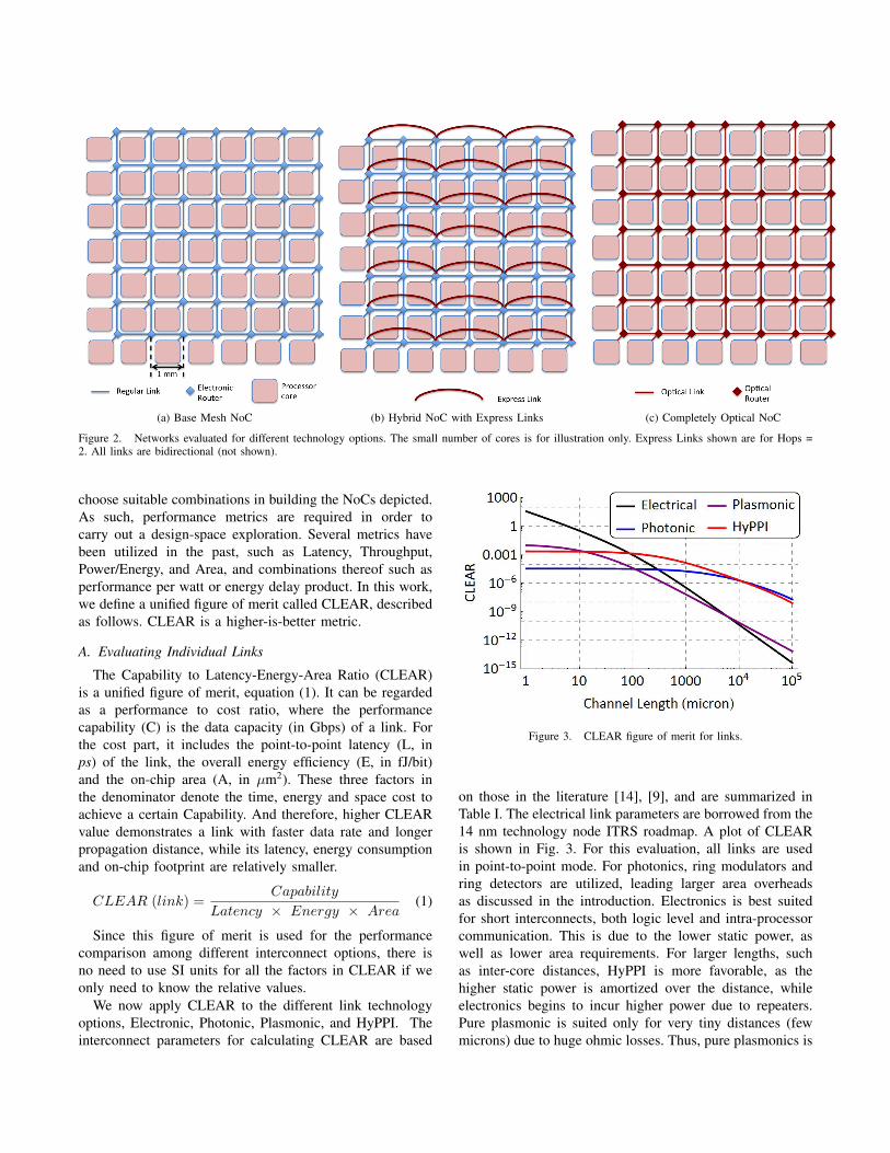
(a) Base Mesh NoC (b) Hybrid NoC with Express Links (c) Completely Optical NoC
Figure 2. Networks evaluated for different technology options. The small number of cores is for illustration only. Express Links shown are for Hops =2. All links are bidirectional (not shown).
choose suitable combinations in building the NoCs depicted.As such, performance metrics are required in order tocarry out a design-space exploration. Several metrics havebeen utilized in the past, such as Latency, Throughput,Power/Energy, and Area, and combinations thereof such asperformance per watt or energy delay product. In this work,we define a unified figure of merit called CLEAR, describedas follows. CLEAR is a higher-is-better metric.
A. Evaluating Individual Links
The Capability to Latency-Energy-Area Ratio (CLEAR)is a unified figure of merit, equation (1). It can be regardedas a performance to cost ratio, where the performancecapability (C) is the data capacity (in Gbps) of a link. Forthe cost part, it includes the point-to-point latency (L, inps) of the link, the overall energy efficiency (E, in fJ/bit)and the on-chip area (A, in µm2). These three factors inthe denominator denote the time, energy and space cost toachieve a certain Capability. And therefore, higher CLEARvalue demonstrates a link with faster data rate and longerpropagation distance, while its latency, energy consumptionand on-chip footprint are relatively smaller.
CLEAR (link) =Capability
Latency × Energy × Area(1)
Since this figure of merit is used for the performancecomparison among different interconnect options, there isno need to use SI units for all the factors in CLEAR if weonly need to know the relative values.
We now apply CLEAR to the different link technologyoptions, Electronic, Photonic, Plasmonic, and HyPPI. Theinterconnect parameters for calculating CLEAR are based
Figure 3. CLEAR figure of merit for links.
on those in the literature [14], [9], and are summarized inTable I. The electrical link parameters are borrowed from the14 nm technology node ITRS roadmap. A plot of CLEARis shown in Fig. 3. For this evaluation, all links are usedin point-to-point mode. For photonics, ring modulators andring detectors are utilized, leading larger area overheadsas discussed in the introduction. Electronics is best suitedfor short interconnects, both logic level and intra-processorcommunication. This is due to the lower static power, aswell as lower area requirements. For larger lengths, suchas inter-core distances, HyPPI is more favorable, as thehigher static power is amortized over the distance, whileelectronics begins to incur higher power due to repeaters.Pure plasmonic is suited only for very tiny distances (fewmicrons) due to huge ohmic losses. Thus, pure plasmonics is
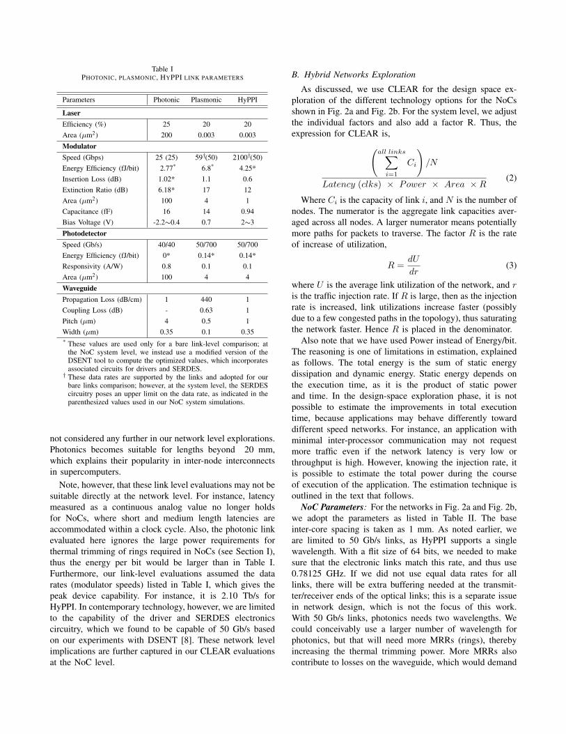
Table IPHOTONIC, PLASMONIC, HYPPI LINK PARAMETERS
Parameters Photonic Plasmonic HyPPI
LaserEfficiency (%) 25 20 20Area (µm2) 200 0.003 0.003
ModulatorSpeed (Gbps) 25 (25) 59†(50) 2100†(50)Energy Efficiency (fJ/bit) 2.77* 6.8* 4.25*Insertion Loss (dB) 1.02* 1.1 0.6Extinction Ratio (dB) 6.18* 17 12Area (µm2) 100 4 1Capacitance (fF) 16 14 0.94Bias Voltage (V) -2.2∼0.4 0.7 2∼3
PhotodetectorSpeed (Gb/s) 40/40 50/700 50/700Energy Efficiency (fJ/bit) 0* 0.14* 0.14*Responsivity (A/W) 0.8 0.1 0.1Area (µm2) 100 4 4
WaveguidePropagation Loss (dB/cm) 1 440 1Coupling Loss (dB) - 0.63 1Pitch (µm) 4 0.5 1Width (µm) 0.35 0.1 0.35* These values are used only for a bare link-level comparison; at
the NoC system level, we instead use a modified version of theDSENT tool to compute the optimized values, which incorporatesassociated circuits for drivers and SERDES.† These data rates are supported by the links and adopted for our
bare links comparison; however, at the system level, the SERDEScircuitry poses an upper limit on the data rate, as indicated in theparenthesized values used in our NoC system simulations.
not considered any further in our network level explorations.Photonics becomes suitable for lengths beyond 20 mm,which explains their popularity in inter-node interconnectsin supercomputers.
Note, however, that these link level evaluations may not besuitable directly at the network level. For instance, latencymeasured as a continuous analog value no longer holdsfor NoCs, where short and medium length latencies areaccommodated within a clock cycle. Also, the photonic linkevaluated here ignores the large power requirements forthermal trimming of rings required in NoCs (see Section I),thus the energy per bit would be larger than in Table I.Furthermore, our link-level evaluations assumed the datarates (modulator speeds) listed in Table I, which gives thepeak device capability. For instance, it is 2.10 Tb/s forHyPPI. In contemporary technology, however, we are limitedto the capability of the driver and SERDES electronicscircuitry, which we found to be capable of 50 Gb/s basedon our experiments with DSENT [8]. These network levelimplications are further captured in our CLEAR evaluationsat the NoC level.
B. Hybrid Networks Exploration
As discussed, we use CLEAR for the design space ex-ploration of the different technology options for the NoCsshown in Fig. 2a and Fig. 2b. For the system level, we adjustthe individual factors and also add a factor R. Thus, theexpression for CLEAR is,
(all links∑
i=1
Ci
)/N
Latency (clks) × Power × Area ×R (2)
Where Ci is the capacity of link i, and N is the number ofnodes. The numerator is the aggregate link capacities aver-aged across all nodes. A larger numerator means potentiallymore paths for packets to traverse. The factor R is the rateof increase of utilization,
R =dU
dr(3)
where U is the average link utilization of the network, and ris the traffic injection rate. If R is large, then as the injectionrate is increased, link utilizations increase faster (possiblydue to a few congested paths in the topology), thus saturatingthe network faster. Hence R is placed in the denominator.
Also note that we have used Power instead of Energy/bit.The reasoning is one of limitations in estimation, explainedas follows. The total energy is the sum of static energydissipation and dynamic energy. Static energy depends onthe execution time, as it is the product of static powerand time. In the design-space exploration phase, it is notpossible to estimate the improvements in total executiontime, because applications may behave differently towarddifferent speed networks. For instance, an application withminimal inter-processor communication may not requestmore traffic even if the network latency is very low orthroughput is high. However, knowing the injection rate, itis possible to estimate the total power during the courseof execution of the application. The estimation technique isoutlined in the text that follows.
NoC Parameters: For the networks in Fig. 2a and Fig. 2b,we adopt the parameters as listed in Table II. The baseinter-core spacing is taken as 1 mm. As noted earlier, weare limited to 50 Gb/s links, as HyPPI supports a singlewavelength. With a flit size of 64 bits, we needed to makesure that the electronic links match this rate, and thus use0.78125 GHz. If we did not use equal data rates for alllinks, there will be extra buffering needed at the transmit-ter/receiver ends of the optical links; this is a separate issuein network design, which is not the focus of this work.With 50 Gb/s links, photonics needs two wavelengths. Wecould conceivably use a larger number of wavelength forphotonics, but that will need more MRRs (rings), therebyincreasing the thermal trimming power. More MRRs alsocontribute to losses on the waveguide, which would demand

Table IINETWORK PARAMETERS USED FOR ALL NOCS IN THIS WORK
Parameters Value
Nodes# Nodes 16×16 (256 nodes)Core Spacing 1 mmCore Clk Freq 0.78125 GHz
RouterFlit Size 64 bits# Ports 5 (base) or 7 (hybrid)# Virtual Channels (VCs) 4Buffers per VC 8 flitsPipeline Depth 3 stagesArea From Modified-DSENTStatic Power From Modified-DSENTDynamic Energy per Flit From Modified-DSENT
LinkLatency 1 clk Elec.,else 2 clksCapacity 50 Gb/sArea From Modified-DSENTStatic Power From Modified-DSENTDynamic Energy per Flit From Modified-DSENT
Figure 4. Hybrid NoC Router with Optical Express Links.
higher laser power. For energy and area estimations, we usedthe DSENT tool [8] for an accurate analysis, using 11 nmtechnology node. For HyPPI, we modified DSENT basedon the component parameters listed in Table I (except, ofcourse, the energy efficiency numbers listed in the table,because power is computed by DSENT; photonic modulatorinsertion loss and extinction ratio are also optimized byDSENT).
The latency value for electronic links is 1 clock cycle.The architecture of the hybrid router, with base electronicsaugmented by optical express links, is shown in Fig. 4. Onlytwo virtual channels are shown for simplicity; router param-eters are listed in Table II. As depicted, the basic routingalways uses electronics. Since express links are bidirectional,
the hybrid router needs two additional ports. For opticalexpress links, an additional clock cycle is required for O-Econversion at the receiver. At the sending end, the routeroutput buffer already has a register which is utilized as astaging area for the transmitter, and thus the transmitterpipeline is already accounted for within the router delay.This is an accurate assumption because each link has adedicated router port. Each E-O conversion implies an on-chip laser. The link propagation delay, for all lengths that weconsider, is bounded within one clock period (i.e. 1 clock@ 0.78125 GHz). Thus the total latency for all optical linksis 2 clock cycles.
Evaluation Methodology: With the different networksas set up in Fig. 2a and Fig. 2b, we then used synthetictraffic statistics to model input traffic, based on Soteriou et.al [15], with p = 0.02 σ = 0.4. The value of p signifies theacceptance probability of a flit, and thus captures the spatialhop distribution. Low p implies longer hops. The value ofσ gives the standard deviation of the traffic injection whichfollows a gaussian distribution; a larger value implies morenodes are injecting traffic. The maximum injection rate isset to 0.1. This value is typical for NoCs, and capturingthe benefits of optical networks at these injection ratesis crucial [8] since optical links have high static power.Optical links (such as nanophotonics and HyPPI) typicallyshow good performance at high injection rates, since thestatic power is amortized across their high data rate. Hencerealistic injection ratios are important. For the traffic model,we used only flit counts between source-destination pairs,and temporal information is ignored (except for the injectionrate).
After setting up the traffic, each network was then ana-lyzed in order to compute the resulting injection rate acrossevery link in the network. An oblivious shortest-path routingmethod was adopted, in order to match the routing techniqueused in the BookSim 2.0 simulator [16] for custom networks,the simulator we use in a later section in this paper.
Based on the injection rate information obtained for eachlink, the power consumption was computed based on thestatic power and dynamic energy per flit numbers fromDSENT. This was carried out across all network compo-nents, the links and routers.
Based on the resulting estimate for the average utilizationof the network, R was also calculated according to equa-tion (3). The average latency is also estimated based on theshortest paths, using the individual latency values for thelinks and routers.
Base Mesh: Based on the outlined methodology, wecomputed CLEAR using equation (2) for the base meshnetwork created using different technologies. Results areshown in Fig. 5, first bar. The units used were, Gb/s forC, clks for L, Watts for E (power), and mm2 for A. Therespective Latency, Power, and Area values are also shownin Fig. 5, in order to understand the CLEAR trends. The

(a) CLEAR: Base E-Mesh + Express (b) CLEAR: Photonic Mesh + Express (c) CLEAR: HyPPI Base Mesh + Express
(d) Latency: Base E-Mesh + Express (e) Latency: Photonic Mesh + Express (f) Latency: HyPPI Base Mesh + Express
(g) Power: Base E-Mesh + Express (h) Power: Photonic Mesh + Express (i) Power: HyPPI Base Mesh + Express
(j) Area: Base E-Mesh + Express (k) Area: Photonic Mesh + Express (l) Area: HyPPI Base Mesh + Express
Figure 5. Comparing different flavors of hybrid NoCs (injection rate = 0.1).

Table IIICAPABILITY (C) AND RATE OF UTILIZATION INCREASE (R)
ParameterExpress Links Topology Plain
3 Hops 5 Hops 15 Hops Mesh
C (Gb/s) 218.75 206.25 193.75 187.5R 0.808 0.885 1.050 1.122
Capability (C) and Rate of utilization increase (R) are fixedfor a given topology across all technology options, andare summarized in Table III. We observe that for the basemesh network, HyPPI seems to be the best option in termsof CLEAR. Note that the routers are still electronic, forall cases considered. Despite the large number of O-E-O conversions, HyPPI being a plasmonic interconnect haslower energy requirements (comparable to electronics) andalso has a much smaller footprint, thus demonstrating a largeCLEAR. The latency, however, is poorer for both the opticalinterconnects (photonics and HyPPI), due to the O-E-Oconversion overheads resulting in an additional clock cycleper hop. Nevertheless, HyPPI fares very well in terms ofarea, as each waveguide of HyPPI has less than 5µm width(including the pitch). On the other hand, each electronic wireis 160nm wide with 160nm spacing, and thus a 64-bit linkrequires around 20µm in width, thus giving a larger areaoverhead for the network. Photonics has a larger footprintthan HyPPI and high static power overhead, and thus farespoorly. We also varied the injection rate from 0.01 to 0.1,and noticed only a small reduction in CLEAR value withthe injection rate, and hence we did not plot those here.
Hybrid NoCs: We explored the various hybrid NoCsusing different technologies for the base Mesh network.With a fixed base network, we tried out Express Links usingall four technology options, with different number of hops.Note that the base network Mesh can use any technology.We observe some interesting trends here. Consider the baseelectronic mesh augmented with express links of differenttechnology types, outputs shown in Fig. 5a,5d,5g, and 5j.Augmenting with photonics long links is the worst optionin terms of CLEAR, poorer than electronic long links. Wecan attribute this to a significant increase in power dueto the photonics links. On the other hand, a reverse trendis observed when we adopt photonics as the base meshnetwork, Fig. 5b,5e,5h, and 5k. Here, using photonics forlong links only improves CLEAR, compared with addingelectronic long links. This is due to the fact that the basephotonic mesh already expends a lot of power, hence theadded long links do not considerably increase the power; butthey add benefits in terms of reduced area compared withlong link electronics. Photonics uses only one waveguideper link, and thus needs less space. In all the plots, wenotice that increasing the hop length reduces CLEAR. Thisis because there are fewer long links incorporated when thenumber of hops is higher (thus, capacity C is lower, and
Table IVSTATIC POWER, WITH ELECTRONIC BASE MESH + EXPRESS LINKS OF
DIFFERENT TECHNOLOGIES
Express Links Total NoC Static Power (W)Technology 3 Hops 5 Hops 15 Hops
Electronic 1.532 1.533 1.547Photonic 3.076 2.458 1.839HyPPI 1.545 1.539 1.533
Static Power for Base Electronic Mesh: 1.53 W
R is higher, see Table III). For instance, in a 16×16 NoC,with Hops=3 we have 5 waveguides per direction in eachrow (see Figure 2b); whereas with Hops=5, we have only 3waveguides per direction in each row. We need waveguidesfor each direction to ensure that the links are bidirectional.
In all cases, we note that HyPPI as the base mesh networkprovides the best results in terms of CLEAR value. However,if the lowest latency is the target, then a base electronic meshis the better option, augmented with HyPPI links to minimizearea and power overheads. In terms of total power, the baseHyPPI and base electronic options are similar. Area-wise,the base HyPPI mesh with augmented HyPPI links givesthe lowest overhead.
The final choice of hybridization depends on the specificrequirements. For further analysis, we use an Electronic basemesh keeping performance (low latency) as the target. Aswe can see in Figure 5, augmenting an electronic mesh withHyPPI can give a CLEAR improvement by up to 1.8× (forExpress Hops = 3).
IV. EXPERIMENTAL RESULTS
In order to evaluate the hybrid NoCs further, we useElectronics as the base technology, and augment it withexpress links. For NoC simulations, we use traces frombenchmark suites that run on parallel HPC platforms. Weuse BookSim 2.0 simulator [16] in trace mode to obtainlatency estimates. The network parameters are as listedin Table II. For energy estimates, we obtain the dynamicenergy consumption per flit from our modified DSENT, anduse it to compute the total dynamic energy based on thecommunication volume and the network paths taken by theflits. Static power consumption for the different networks issummarized in Table IV. All traffic traces are based on 256-node benchmarks, as the network has a 16×16 configuration.
We used the NAS Parallel Benchmarks (NPB) [17],Class A workloads. The following kernels were used - FT,CG, MG, and LU. These benchmarks were executed on aCray XE6m supercomputer and traffic traces obtained usingMPICL. The traces were then converted into BookSim-compatible traces. At times, the traces contained packets thatwere of very large size (hundreds of kilobytes). Such packetswere broken down into smaller packets. For simplicity, allsimulations used two types of packets - 1 flit per packet

Figure 6. Average Latency for NAS Parallel Benchmarks. The opticaltechnology in O-Mesh could be either Photonics or HyPPI.
Table VDYNAMIC ENERGY, FT BENCHMARK
Express Links Total Dynamic Energy (J)Technology 3 Hops 5 Hops 15 Hops
Electronic 0.0054 0.0066 0.0128Photonic 0.9353 0.9353 0.9353HyPPI 0.0049 0.0049 0.0049
Dynamic Energy for Plain (Base) Electronic Mesh: 0.0042 J
and 32 flits per packet. All large packets from the origi-nal network trace were split up into smaller packets, andinjected into the network at their respective source nodes,respecting the link bandwidths. The inter-node and intra-node bandwidth in the Cray is in the range 10-13 GB/s,which exceeds our link bandwidth (50 Gb/s, or 6 GB/s), sothe traces will not saturate the NoC simulator.
A. Latency
The latency results for the networks are summarized inFig. 6. Latency in clock cycles is shown for base ElectronicMesh, as well as Express Links NoCs with Hops = 3,5, and 15. Hops=15 makes the network effectively a 2Dtorus. The optical express links could use either photonics orHyPPI. The latency is the same in both cases, because theirindividual link latencies are identical (2 clks) as previouslynoted. Thus we don’t differentiate between them in Fig. 6.As expected, adding express links reduces the averagelatency. The CG benchmark has short range traffic and isthus benefited maximum by Hops=3, showing a latencyreduction by a factor of 1.25×. On the other hand, MGhas long range traffic and thus benefits from longer hops,exhibiting a 1.64× latency reduction for Hops=15. The LUbenchmark is almost completely comprised of 1-hop traffic,
and thus doesn’t derive significant latency improvements.On the other hand, FT has all-to-all traffic, and thus benefitsfrom all types of express links, with a maximum of 1.3×using Hops=15.
B. Energy
Augmenting the electronic mesh thus brings notable ben-efits to latency for real applications. To check whetherthese improvements come at the cost of energy, we lookat the results for the FT benchmark in the NPB suite,Table V. Compared to the base mesh, the hybrid NoC withHyPPI-based express links hardly shows any increase in therelative dynamic energy. In addition, the static power of theelectronic mesh is 1.53 W, which is not significantly lowerthan the 1.533-1.545 W for the hybrid NoC with HyPPIexpress links, see Table IV. The trends in dynamic energyfor the other benchmarks of the NPB suite are very muchsimilar, and are thus not reported here.
Adopting an electronic base mesh with HyPPI expresslinks is therefore an excellent option for building hybridNoCs. It is still a hybrid network, and incurs overheads forO-E-O conversion at every hop. Fully optical NoCs couldpotentially provide higher performance, energy, and areabenefits, and we explore this further in the next section.
V. PROJECTIONS FOR ALL-OPTICAL NOCS
Fully optical NoCs, comprised of optical routers and links,are a promising option that need to be evaluated further.Specifically, designers can better leverage the advantagesof photonics by using its routing capabilities based onmultiple wavelengths, or WDM. There have been all opticalNoCs proposed in the literature [1]; however, all of themuse a variety of values for the optical parameters makingcomparisons difficult, as described in our prior work [18].So we instead construct our own all-optical NoC, Fig. 2c,and use a uniform set of parameters. All-optical NoCs arefundamentally circuit-switched, which means that a pathbetween a source and destination needs to be first establishedbefore initiating bulk transfer of packets. Once the path isset up, the latency is one clock cycle or few clock cycles,depending on the path length. However, the exact latencysavings is application dependent. Moreover, photonics withring resonators are very bulky as noted in Section I, andphotonic routers typically deploy a large number of rings.Thus, photonic NoCs may not be a very attractive option.All-photonic NoCs may also have other disadvantages, asnoted in the beginning of Section III.
However, HyPPI, with its tiny device footprint, can beadvantageous for all-optical NoCs. In order evaluate anall-HyPPI NoC, we need a router. We designed a routerbased on prior art [19]. The building block is our ultra-compact plasmonic electro-optical 2 × 2 switch [20]. Thedevice operates by tuning the coupling length between twoSOI waveguide busses by changing the effective index of a

Figure 7. HyPPI Router.
MOS plasmonic island electrically. Due to the compact size(< 5µm) this switch has fJ/bit power consumption and psswitching delay times. The designed router is depicted inFigure 7, summarized in Table VI. The corresponding pho-tonic router characteristics, which uses 8 rings to realize theeight 2×2 switches [21], are also summarized in the table.The loss incurred by light propagating through the routerdepends on the input and output port selected. Although theHyPPI router shows potentially larger losses, we are able touse an optimal port assignment (mapping of router ports tothe NoC node ports) to incur minimal losses, assuming X-Ydimension ordered routing strategy†. Further details of thisrouter are beyond the scope of this paper.
Table VICOMPARISON OF WDM-BASED PHOTONIC AND HYPPI ROUTERS
Technology Control Energy Loss Range Area(fJ/bit) (dB) (µm2)
Photonic 68.2 0.39-1.5 480,000
HyPPI 3.73 0.32-9.1 500
We then estimated the energy consumption for 16×16 all-optical NoCs for the synthetic traffic used in Section III-B.In order to do so, the losses incurred along the entire pathfrom source to destination for each flit was computed, andthe laser power was estimated accordingly using HyPPIand photonic energy equations [9]. Latency values are morechallenging to estimate, since the optical path setup willincur overheads. Nevertheless, previously published resultsreported around 50% reduction in latency over an electronicmesh, with an all-optical NoC using an electronic controlnetwork for path setup [22]. We adopt this approximationin our estimates. The area is estimated by using the opticalrouter parameters from Table VI, and the electronic routerparameters from the DSENT tool [8].
A comparison of the three networks - electronic mesh,all-photonic NoC, and all-HyPPI NoC - is shown through aradar plot in Fig. 8. Since all the three parameters, namely,Latency, Energy/bit, and Area, are cost values, they need tobe small. Thus a triangle with a smaller enclosed area is thebetter option. From the figure, we note that all-HyPPI has
†U-turns are not implemented, e.g. connection from Port 1 to Port 1.
Figure 8. All-Optical WDM NoC vs. Electronic NoC. The triangle thatencloses smaller area is the better option.
the potential to significantly outperform the other two NoCs.In terms of energy, all-photonic and all-HyPPI are close,at 352 fJ/bit and 354 fJ/bit respectively, whereas electronicmesh requires 89.7 nJ/bit. Area-wise, all-HyPPI fares verywell with 1.24 mm2. Electronic mesh needs 22.1 mm2,while the all-photonic mesh needs 127.7 mm2. Thus, if all-optical NoCs are to be considered in the future, HyPPI is anexcellent candidate for serving as the technology of choice.
VI. CONCLUSIONS
In this paper, we explored new optical link technol-ogy options for augmenting on-chip network topologies,namely, hybrid plasmonics - an optical interconnect thatuses plasmonics for active data manipulation and diffraction-limited photonics for passive propagation (HyPPI). Next, inorder to help design hybrid networks incorporating expresslinks, we adopted a unified metric called CLEAR, anddemonstrated results for link and network evaluations usingthis metric. These evaluations demonstrated that electronicNoCs augmented with HyPPI provided a 1.8× improvementin CLEAR over a base electronic mesh. In carrying outour evaluations, we modified the DSENT tool for modelingHyPPI, in order to obtain accurate energy and area estimates.Then, network level simulations were carried out on theBookSim 2.0 simulator, based on traffic traces from theNAS Parallel Benchmark suite. These results indicated upto 1.64× latency improvement over a base electronic mesh,with negligible energy overheads due to the HyPPI expresslinks. Finally, we carried out performance projections forall-optical NoCs. The projections indicate that all-HyPPIas well as all-photonic NoCs would be significantly moreenergy efficient than electronic NoCs (255×), althoughelectronic route setup requirements may diminish this result.Furthermore, an all-HyPPI NoC would be two orders ofmagnitude smaller in area compared with an all-photonic

NoC, and one order of magnitude smaller than an electronicNoC. Thus, HyPPI was demonstrated to be an excellenttechnology choice for the future, for both hybrid NoCs aswell as all-optical NoCs.
VII. ACKNOWLEDGMENTS
This work was partially supported by the Air Force Officeof Scientific Research (AFOSR) under Award FA9550-15-1-0447.
REFERENCES
[1] C. J. Nitta, M. K. Farrens, and V. Akella, On-Chip PhotonicInterconnects: A Computer Architect’s Perspective (book),Synthesis Lectures on Computer Architecture series. Morgan& Claypool Publishers, 2013.
[2] D. Vantrease, R. Schreiber, M. Monchiero, M. McLaren, N. P.Jouppi, M. Fiorentino, A. Davis, N. Binkert, R. G. Beausoleil,and J. H. Ahn, “Corona: System Implications of EmergingNanophotonic Technology,” in Proceedings of the 35th An-nual International Symposium on Computer Architecture, ser.ISCA ’08, 2008, pp. 153–164.
[3] C. Li, M. Browning, P. V. Gratz, and S. Palermo, “LumiNOC:A Power-Efficient, High-Performance, Photonic Network-on-Chip for Future Parallel Architectures,” in 21st internationalconference on Parallel Architectures and Compilation Tech-niques (PACT). ACM, 2012, pp. 421–422.
[4] Y. Pan, J. Kim, and G. Memik, “Flexishare: Channel Sharingfor an Energy-efficient Nanophotonic Crossbar,” in HPCA -16 2010 The Sixteenth International Symposium on High-Performance Computer Architecture, Jan 2010, pp. 1–12.
[5] G. Kurian, J. E. Miller, J. Psota, J. Eastep, J. Liu, J. Michel,L. C. Kimerling, and A. Agarwal, “ATAC: A 1000-coreCache-coherent Processor with On-chip Optical Network,” in19th international conference on Parallel Architectures andCompilation Techniques (PACT). ACM, 2010, pp. 477–488.
[6] P. Dong, S. Liao, D. Feng, H. Liang, D. Zheng, R. Shafiiha,C.-C. Kung, W. Qian, G. Li, X. Zheng et al., “Low Vpp,Ultralow-energy, Compact, High-speed Silicon Electro-opticModulator,” Optics Express, vol. 17, no. 25, pp. 22 484–22 490, 2009.
[7] P. Dong, W. Qian, H. Liang, R. Shafiiha, N.-N. Feng, D. Feng,X. Zheng, A. V. Krishnamoorthy, and M. Asghari, “Lowpower and compact reconfigurable multiplexing devices basedon silicon microring resonators,” Optics express, vol. 18,no. 10, pp. 9852–9858, 2010.
[8] C. Sun, C.-H. O. Chen, G. Kurian, L. Wei, J. Miller,A. Agarwal, L.-S. Peh, and V. Stojanovic, “DSENT - A ToolConnecting Emerging Photonics with Electronics for Opto-Electronic Networks-on-Chip Modeling,” in 6th IEEE/ACMInternational Symposium on Networks on Chip (NoCS).IEEE, 2012, pp. 201–210.
[9] S. Sun, A.-H. A. Badawy, V. Narayana, T. El-Ghazawi, andV. J. Sorger, “The Case for Hybrid Photonic Plasmonic Inter-connects (HyPPIs): Low-latency Energy-and-Area-EfficientOn-Chip Interconnects,” IEEE Photonics Journal, vol. 7,no. 6, pp. 1–14, 2015.
[10] C. Ye, S. Khan, Z. R. Li, E. Simsek, and V. J. Sorger, “λ-sizeITO and Graphene-based Electro-optic Modulators on SOI,”IEEE Journal of Selected Topics in Quantum Electronics,vol. 20, no. 4, pp. 40–49, 2014.
[11] B. Grot, J. Hestness, S. W. Keckler, and O. Mutlu, “ExpressCube Topologies for On-chip Interconnects,” in 2009 IEEE15th International Symposium on High Performance Com-puter Architecture. IEEE, 2009, pp. 163–174.
[12] M. Kennedy and A. K. Kodi, “Bandwidth Adaptive Nanopho-tonic Crossbars with Clockwise/Counter-clockwise OpticalRouting,” in 28th International Conference on VLSI Design(VLSID). IEEE, 2015, pp. 123–128.
[13] J. Chan, G. Hendry, A. Biberman, K. Bergman, and L. P.Carloni, “PhoenixSim: A Simulator for Physical-layer Anal-ysis of Chip-scale Photonic Interconnection Networks,” inProceedings of the Conference on Design, Automation andTest in Europe, ser. DATE ’10, 2010, pp. 691–696.
[14] G. Chen, H. Chen, M. Haurylau, N. A. Nelson, D. H.Albonesi, P. M. Fauchet, and E. G. Friedman, “Predictionsof CMOS Compatible On-chip Optical Interconnect,” Inte-gration, the VLSI Journal, vol. 40, no. 4, pp. 434–446, Jul.2007.
[15] V. Soteriou, H. Wang, and L. Peh, “A Statistical Traffic Modelfor On-chip Interconnection Networks,” in 14th IEEE Inter-national Symposium on Modeling, Analysis, and Simulation.IEEE, 2006, pp. 104–116.
[16] N. Jiang, D. U. Becker, G. Michelogiannakis, J. Balfour,B. Towles, D. E. Shaw, J.-H. Kim, and W. J. Dally, “ADetailed and Flexible Cycle-accurate Network-on-Chip Sim-ulator,” in International Symposium on Performance Analysisof Systems and Software (ISPASS). IEEE, 2013, pp. 86–96.
[17] NASA, “NAS Parallel Benchmarks,” accessed 2016. [Online].Available: http://www.nas.nasa.gov/publications/npb.html
[18] V. K. Narayana, S. Sun, A.-H. A. Badawy, V. J. Sorger, andT. El-Ghazawi, “MorphoNoC: Exploring the design space of aconfigurable hybrid NoC using nanophotonics,” To appear inMicroprocessors and Microsystems, arXiv:1701.05930, 2017.
[19] R. Soref, “Mid-infrared 2× 2 electro-optical switching bysilicon and germanium three-waveguide and four-waveguidedirectional couplers using free-carrier injection,” PhotonicsResearch, vol. 2, no. 5, pp. 102–110, 2014.
[20] C. Ye, K. Liu, R. A. Soref, and V. J. Sorger, “A CompactPlasmonic MOS-based 2×2 Electro-optic Switch,” Nanopho-tonics, vol. 4, no. 1, pp. 261–268, 2015.
[21] H. Jia, Y. Zhao, L. Zhang, Q. Chen, J. Ding, X. Fu, andL. Yang, “Five-port Optical Router Based on Silicon Micror-ing Optical Switches for Photonic Networks-on-Chip,” IEEEPhotonics Technology Letters, vol. 28, no. 9, pp. 947–950,May 2016.
[22] Z. Chen, H. Gu, Y. Yang, L. Bai, and H. Li, “A PowerEfficient and Compact Optical Interconnect for Network-on-Chip,” IEEE Computer Architecture Letters, vol. 13, no. 1,pp. 5–8, Jan 2014.