hyperstone e1 e1---32xs / e132xs / e132xs / e1-- · pdf file1-2 chapter 1 1.1. introduction...
TRANSCRIPT

hyperstonestonestonestone E1 E1 E1 E1----32XS / E132XS / E132XS / E132XS / E1----16XS16XS16XS16XS
32-Bit-RISC/DSP Microprocessor User's Manual

Specifications and information in this document are subject to change without notice and do not represent a commitment on the part of Hyperstone AG. Hyperstone AG reserves the right to make changes to improve functioning. Although the information in this document has been carefully reviewed, Hyperstone AG does not assume any liability arising out of the use of the product or circuit described herein.
Hyperstone AG does not authorize the use of the Hyperstone microprocessor in life support applications wherein a failure or malfunction of the microprocessor may directly threaten life or cause injury. The user of the Hyperstone microprocessor in life support applications assumes all risks of such use and indemnifies Hyperstone AG against all damages.
No part of this manual may be reproduced or transmitted in any form or by any means, electronic or mechanical, including photo-copying and recording, for any purpose without the permission of Hyperstone AG.
Hyperstone is a registered trademark of Hyperstone AG
For further information please contact:
Hyperstone AG Line-Eid-Strasse 3 D-78467 Konstanz Germany Phone (+49) 7531 / 9803-0 Fax (+49) 7531 / 51725 E-Mail [email protected]
www.hyperstone.com
Copyright 1990, 2002 Hyperstone AG
Revision 09/2002

TABLE OF CONTENTS i
Table of Contents 1. Architecture
1.1. Introduction ........................................................................................................ 1-1 1.2. Block Diagram ................................................................................................... 1-7 1.3. Global Register Set ............................................................................................ 1-8
1.3.1. Program Counter PC.............................................................................. 1-9 1.3.2. Status Register SR ............................................................................... 1-10 1.3.3. Floating-Point Exception Register FER .............................................. 1-13 1.3.4. Stack Pointer SP .................................................................................. 1-13 1.3.5. Upper Stack Bound UB ....................................................................... 1-13 1.3.6. Bus Control Register BCR................................................................... 1-13 1.3.7. Timer Prescaler Register TPR ............................................................. 1-14 1.3.8. Timer Compare Register TCR............................................................. 1-14 1.3.9. Timer Register TR ............................................................................... 1-14 1.3.10. Watchdog Compare Register WCR................................................... 1-14 1.3.11. Input Status Register ISR................................................................... 1-14 1.3.12. Function Control Register FCR......................................................... 1-14 1.3.13. Memory Control Register MCR ........................................................ 1-14
1.4. Local Register Set ............................................................................................ 1-15 1.5. Privilege States................................................................................................. 1-16 1.6. Register Data Types ......................................................................................... 1-17 1.7. Memory Organization ...................................................................................... 1-18 1.8. Stack................................................................................................................. 1-20 1.9. Instruction Cache.............................................................................................. 1-25 1.10. On-Chip Memory (IRAM) ............................................................................. 1-27
2. Instructions General 2.1. Instruction Notation............................................................................................ 2-1 2.2. Instruction Execution ......................................................................................... 2-2 2.3. Instruction Formats ............................................................................................ 2-3
2.3.1. Table of Immediate Values.................................................................... 2-5 2.3.2. Table of Instruction Codes..................................................................... 2-6 2.3.3. Table of Extended DSP Instruction Codes ............................................ 2-7
2.4. Entry Tables ....................................................................................................... 2-8 2.5. Instruction Timing............................................................................................ 2-12
3. Instruction Set 3.1. Memory Instructions .......................................................................................... 3-1
3.1.1. Address Modes ...................................................................................... 3-2 3.1.2. Load Instructions ................................................................................... 3-6 3.1.3. Store Instructions ................................................................................... 3-8
3.2. Move Word Instructions................................................................................... 3-10 3.3. Move Double-Word Instruction ....................................................................... 3-10 3.4. Logical Instructions.......................................................................................... 3-11 3.5. Invert Instruction .............................................................................................. 3-12 3.6. Mask Instruction............................................................................................... 3-12

ii TABLE OF CONTENTS
3.7. Add Instructions............................................................................................... 3-13 3.8. Sum Instructions .............................................................................................. 3-15 3.9. Subtract Instructions ........................................................................................ 3-16 3.10. Negate Instructions ........................................................................................ 3-17 3.11. Multiply Word Instruction ............................................................................. 3-18 3.12. Multiply Double-Word Instructions............................................................... 3-18 3.13. Divide Instructions......................................................................................... 3-19 3.14. Shift Left Instructions .................................................................................... 3-20 3.15. Shift Right Instructions .................................................................................. 3-21 3.16. Rotate Left Instruction ................................................................................... 3-22 3.17. Index Move Instructions ................................................................................ 3-23 3.18. Check Instructions ......................................................................................... 3-24 3.19. No Operation Instruction ............................................................................... 3-24 3.20. Compare Instructions ..................................................................................... 3-25 3.21. Compare Bit Instructions ............................................................................... 3-26 3.22. Test Leading Zeros Instruction ...................................................................... 3-26 3.23. Set Stack Address Instruction ........................................................................ 3-27 3.24. Set Conditional Instructions........................................................................... 3-27 3.25. Branch Instructions ........................................................................................ 3-29 3.26. Delayed Branch Instructions .......................................................................... 3-30 3.27. Call Instruction............................................................................................... 3-32 3.28. Trap Instructions ............................................................................................ 3-33 3.29. Frame Instruction ........................................................................................... 3-35 3.30. Return Instruction .......................................................................................... 3-37 3.31. Fetch Instruction ............................................................................................ 3-39 3.32. Extended DSP Instructions ............................................................................ 3-40 3.33. Software Instructions ..................................................................................... 3-42
3.33.1. Do Instruction.................................................................................... 3-43 3.33.2. Floating-Point Instructions ................................................................ 3-44
4. Exceptions 4.1. Exception Processing......................................................................................... 4-1 4.2. Exception Types................................................................................................. 4-2
4.2.1. Reset ...................................................................................................... 4-2 4.2.2. Range, Pointer, Frame and Privilege Error............................................ 4-2 4.2.3. Extended Overflow................................................................................ 4-3 4.2.4. Parity Error ............................................................................................ 4-3 4.2.5. Interrupt ................................................................................................. 4-3 4.2.6. Trace Exception..................................................................................... 4-4
4.3. Exception Backtracking ..................................................................................... 4-4
5. Timer 5.1. Overview............................................................................................................ 5-1
5.1.1. Timer Prescaler Register TPR............................................................... 5-1 5.1.2. Timer Register TR................................................................................. 5-2 5.1.3. Timer Compare Register TCR............................................................... 5-3 5.1.4. Power-Down Mode ............................................................................... 5-3 5.1.5. Additional Power Saving....................................................................... 5-4
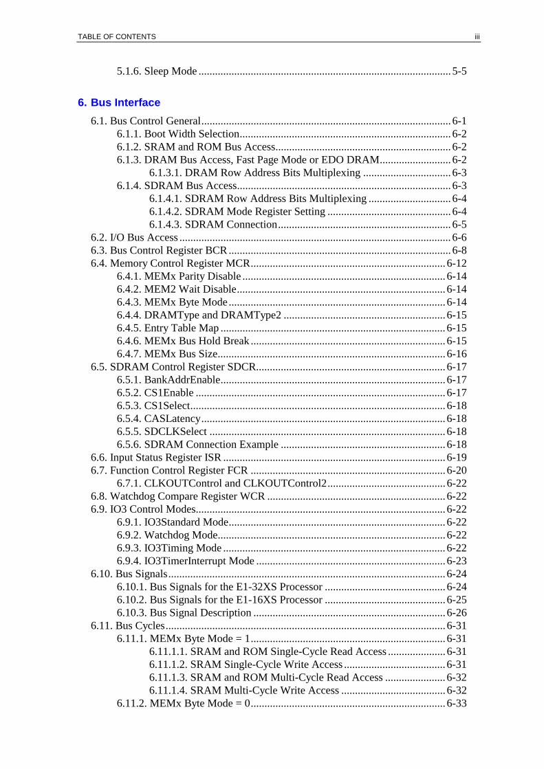
TABLE OF CONTENTS iii
5.1.6. Sleep Mode ............................................................................................ 5-5
6. Bus Interface 6.1. Bus Control General........................................................................................... 6-1
6.1.1. Boot Width Selection............................................................................. 6-2 6.1.2. SRAM and ROM Bus Access................................................................ 6-2 6.1.3. DRAM Bus Access, Fast Page Mode or EDO DRAM.......................... 6-2
6.1.3.1. DRAM Row Address Bits Multiplexing ................................ 6-3 6.1.4. SDRAM Bus Access.............................................................................. 6-3
6.1.4.1. SDRAM Row Address Bits Multiplexing .............................. 6-4 6.1.4.2. SDRAM Mode Register Setting ............................................. 6-4 6.1.4.3. SDRAM Connection............................................................... 6-5
6.2. I/O Bus Access ................................................................................................... 6-6 6.3. Bus Control Register BCR ................................................................................. 6-8 6.4. Memory Control Register MCR....................................................................... 6-12
6.4.1. MEMx Parity Disable .......................................................................... 6-14 6.4.2. MEM2 Wait Disable............................................................................ 6-14 6.4.3. MEMx Byte Mode............................................................................... 6-14 6.4.4. DRAMType and DRAMType2 ........................................................... 6-15 6.4.5. Entry Table Map .................................................................................. 6-15 6.4.6. MEMx Bus Hold Break ....................................................................... 6-15 6.4.7. MEMx Bus Size................................................................................... 6-16
6.5. SDRAM Control Register SDCR..................................................................... 6-17 6.5.1. BankAddrEnable.................................................................................. 6-17 6.5.2. CS1Enable ........................................................................................... 6-17 6.5.3. CS1Select............................................................................................. 6-18 6.5.4. CASLatency......................................................................................... 6-18 6.5.5. SDCLKSelect ...................................................................................... 6-18 6.5.6. SDRAM Connection Example ............................................................ 6-18
6.6. Input Status Register ISR ................................................................................. 6-19 6.7. Function Control Register FCR ....................................................................... 6-20
6.7.1. CLKOUTControl and CLKOUTControl2........................................... 6-22 6.8. Watchdog Compare Register WCR ................................................................. 6-22 6.9. IO3 Control Modes........................................................................................... 6-22
6.9.1. IO3Standard Mode............................................................................... 6-22 6.9.2. Watchdog Mode................................................................................... 6-22 6.9.3. IO3Timing Mode ................................................................................. 6-22 6.9.4. IO3TimerInterrupt Mode ..................................................................... 6-23
6.10. Bus Signals..................................................................................................... 6-24 6.10.1. Bus Signals for the E1-32XS Processor ............................................ 6-24 6.10.2. Bus Signals for the E1-16XS Processor ............................................ 6-25 6.10.3. Bus Signal Description ...................................................................... 6-26
6.11. Bus Cycles...................................................................................................... 6-31 6.11.1. MEMx Byte Mode = 1....................................................................... 6-31
6.11.1.1. SRAM and ROM Single-Cycle Read Access ..................... 6-31 6.11.1.2. SRAM Single-Cycle Write Access ..................................... 6-31 6.11.1.3. SRAM and ROM Multi-Cycle Read Access ...................... 6-32 6.11.1.4. SRAM Multi-Cycle Write Access ...................................... 6-32
6.11.2. MEMx Byte Mode = 0....................................................................... 6-33

iv TABLE OF CONTENTS
6.11.2.1. SRAM Single-Cycle Read Access...................................... 6-33 6.11.2.2. SRAM Single-Cycle Write Access..................................... 6-33 6.11.2.3. SRAM Multi-Cycle Read Access ....................................... 6-34 6.11.2.4. SRAM Multi-Cycle Write Access ...................................... 6-34
6.11.3. MEM2 Read Access with WAIT Pin ................................................ 6-35 6.11.4. I/O Read Access ................................................................................ 6-36 6.11.5. I/O Read Access with WAIT Pin ...................................................... 6-37 6.11.6. I/O Write Access ............................................................................... 6-38 6.11.7. DRAM............................................................................................... 6-39
6.11.7.1. Fast Page Mode DRAM Access ......................................... 6-39 6.11.7.2. EDO DRAM Single-Cycle Access ..................................... 6-40 6.11.7.3. EDO DRAM Multi-Cycle Access ...................................... 6-41 6.11.7.4. Fast Page Mode or EDO DRAM Refresh........................... 6-42 6.11.7.5. SDRAM Access.................................................................. 6-43
6.12. DC Characteristics ......................................................................................... 6-44 6.13. AC Characteristics ......................................................................................... 6-45
6.13.1. Processor Clock and CLKIN ............................................................. 6-45 6.13.2. GRANT# response time .................................................................... 6-45
7. Mechanical Data 7.1. hyperstone E1-32XS, 144-Pin LQFP Package .................................................. 7-1
7.1.1. Pin Configuration - View from Top Side .............................................. 7-1 7.1.2. Pin Cross Reference by Pin Name......................................................... 7-2 7.1.3. Pin Cross Reference by Location .......................................................... 7-3
7.2. hyperstone E1-16XS, 100-Pin LQFP Package .................................................. 7-4 7.2.1. Pin Configuration - View from Top Side .............................................. 7-4 7.2.2. Pin Cross Reference by Pin Name......................................................... 7-5 7.2.3. Pin Cross Reference by Location .......................................................... 7-6
7.3. hyperstone E1-16XSB, 100-Pin TFBGA Package ............................................ 7-7 7.3.1. Pin Configuration – View from Top Side ............................................. 7-7 7.3.2. Pin Cross Reference by Pin Name......................................................... 7-8 7.3.3. Pin Cross Rreference by Location ......................................................... 7-9
7.4. Package Dimensions ........................................................................................ 7-10 7.4.1. Package Dimensions LQFP................................................................. 7-10 7.4.2. Package Dimensions TFBGA.............................................................. 7-12

ARCHITECTURE 1-1
1. Architecture
1.1. Introduction The hyperstone E1-32XS and hyperstone E1-16XS microprocessors represent a further devel-opment of the hyperstone E1-32X and hyperstone E1-16X processors. Using a sophisticated 0.25 µm CMOS process, the maximum clock rate of the processor could be further im-proved. Being pin-compatible to their predecessors these new processors can be used as a direct replacement in existing designs, given that the changed voltage supply requirements are considered.
This combination of a high-performance RISC microprocessor with an additional powerful DSP instruction set and on-chip microcontroller functions offers a high throughput. The speed is obtained by an optimized combination of the following features:
The most recent stack frames are kept in a register stack, thereby reducing data memory accesses to a minimum by keeping almost all local data in registers.
Pipelined memory access allows overlapping of memory accesses with execution.
16 KByte fully static On-Chip Memory (IRAM).
On-chip Instruction Cache omits instruction fetch in inner loops and provides prefetch.
Variable-length instructions of 16, 32 or 48 bits provide a large, powerful instruction set, thereby reducing the number of instructions to be executed.
Primarily used 16-bit instructions halve the memory bandwidth required for instruction fetch in comparison to conventional RISC architectures with fixed-length 32-bit instruc-tions, yielding also even better code economy than conventional CISC architectures.
Orthogonal instruction set.
Most instructions execute in one cycle.
Pipelined DSP instructions.
Parallel execution of ALU, DSP, and load/store instructions.
Single-cycle half-word multiply-accumulate operation.
Fast Call and Return by parameter passing via registers.
An instruction pipeline depth of just two stages — decode/execute — provides branch-ing without insertion of wait cycles in combination with Delayed Branch instructions.
Range and pointer checks are performed without speed penalty, thus, these checks need no longer be turned off, thereby providing higher runtime reliability.
Separate address and data buses provide a throughput of one 32-bit word each cycle.
The features noted above contribute to reduce the number of idle wait cycles to a bare minimum. The processor is designed to sustain its execution rate with a standard SDRAM memory.
The low power consumption is of advantage for mobile (portable) applications or in tem-perature-sensitive environments.
1-2 CHAPTER 1
1.1. Introduction (continued) Most of the transistors are used for the on-chip memory, the instruction cache, the register stack and the multiplier, whereas only a small number is required for the control logic.
Due to their low manufacturing costs, the hyperstone E1-32XS and E1-16XS microproces-sors are very well suited for embedded systems applications requiring high performance and lowest cost. To simplify board design as well as to reduce system costs, the hyper-stone E1-32XS and E1-16XS already come with integrated peripherals, such as a timer and memory and bus control logic. Therefore, complete systems using hyperstone microproces-sors can be designed with a minimum of external components. To connect any kind of memory or I/O, no glue logic is necessary. It is even suitable for systems where up to now microprocessors with 16-bit architecture have been used for cost reasons. Its improved per-formance compared to conventional microcontrollers can be used to software-substitute many external peripherals like graphics controllers or DSPs. Using the hyperstone E1-32XS as a core for ASICs or ASSPs is particularly advantageous because the total gate count of the entire logic is just about 35k gates without the on-chip memory.
The software development tools include an optimizing C compiler, assembler, source-level debugger with profiler as well as a runtime kernel and a sophisticated DSP library. Using the runtime kernel, up to 31 tasks, each with its own virtual timer, can be developed inde-pendently of each other. The synchronization of these tasks is effected almost automatically by the runtime kernel. For the system designer, it seems as if he has up to 31 hyperstone microprocessors to which he can allocate his programs accordingly. Real-time debugging of multiple tasks is assisted in an optimized way. The DSP library provides a powerful set of DSP related functions and is taking care of all parallelism between ALU, DSP, and Load/Store unit.
The following description gives a brief architectural overview:
Compatibility:
Pin compatible to hyperstone E1-32X and hyperstone E1-16X.
Phased Locked Loop:
An internal phased locked loop circuit (PLL) provides clock rate multiplication by a factor ½, 1, 2, 4, or 8. For example, only an external crystal of 12 MHz is required to achieve an internal clock rate of 96 MHz.
Registers:
32 global and 64 local registers of 32 bits each
16 global and up to 16 local registers are addressable directly
Flags:
Zero(Z), negative(N), carry(C) and overflow(V) flag
Interrupt-mode, interrupt-lock, trace-mode, trace-pending, supervisor state, cache-mode and high global flag

ARCHITECTURE 1-3
1.1. Introduction (continued)
Register Data Types:
Unsigned integer, signed integer, single or double signed short, signed complex short, single or double 16-bit fixed-point, bit string, IEEE-754 floating-point, each either 32 or 64 bits
External Memory:
Address space of 4 Gbytes, divided into five areas
Separate I/O address space
Load/Store architecture
Pipelined memory and I/O accesses
High-order data located and addressed at lower address (big endian)
Instructions and double-word data may cross DRAM page boundaries
On-Chip Memory (IRAM):
16 KByte fully static internal memory, 32 bit wide, single cycle access
Memory Data Types:
Unsigned and signed byte (8 bit)
Unsigned and signed half-word (16 bit), located on half-word boundary
Undedicated word (32 bit), located on word boundary
Undedicated double-word (64 bit), located on word boundary
Runtime Stack:
Runtime Stack is divided into memory part and register part
Register part is implemented by the 64 local registers holding the most recent stack frame(s)
Current stack frame (maximum 16 registers) is always kept in register part of the stack
Data transfer between memory and register part of the stack is automatic
Upper stack bound is guarded
Instruction Cache:
An on-chip Instruction Cache reduces instruction memory access substantially
Instructions General:
Variable-length instructions of one, two or three half-words halve required memory bandwidth
Pipeline depth of only two stages, assures immediate refill after branches

1-4 CHAPTER 1
1.1. Introduction (continued) Register instructions of type "source operator destination ⇒ destination" or
"source operator immediate ⇒ destination"
All register bits participate in an operation
Immediate operands of 5, 16 and 32 bits, zero- or sign-expanded
Large address displacement of up to 28 bits
Two sets of signed arithmetical instructions: instructions set or clear either only the overflow flag or trap additionally to a Range Error routine on overflow
DSP instructions operate on 16-bit integer, real and complex fixed-point data and 32-bit integer data into 32-bit and 64-bit hardware accumulators
Instruction Summary:
Memory instructions pipelined to a depth of two stages, trap on address register equal to zero (check for invalid pointers)
Memory address modes: register address, register post-increment, register + dis-placement (including PC relative), register post-increment by displacement (next ad-dress), absolute, stack address, I/O absolute and I/O displacement
Load, all data types, bytes and half-words right adjusted and zero- or sign-expanded, execution proceeds after Load until data is needed
Store, all data types, trap when range of signed byte or half-word is exceeded
Move, Move immediate, Move double-word
Logical instructions AND, AND not, OR, XOR, NOT, AND not immediate, OR imme-diate, XOR immediate
Mask source and immediate ⇒ destination
Add unsigned/signed, Add signed with trap on overflow, Add with carry
Add unsigned/signed immediate, Add signed immediate with trap on overflow
Sum source + immediate ⇒ destination, unsigned/signed and signed with trap on over-flow
Subtract unsigned/signed, Subtract signed with trap on overflow, Subtract with carry
Negate unsigned/signed, Negate signed with trap on overflow
Multiply word ∗ word ⇒ low-order word unsigned or signed, Multiply word ∗ word ⇒ double-word unsigned and signed
Divide double-word by word ⇒ quotient and remainder, unsigned and signed
Shift left unsigned/signed, single and double-word, by constant and by content of regis-ter
Shift right unsigned and signed, single and double-word, by constant and by content of register
Rotate left single word by content of register
Index Move, move an index value scaled by 1, 2, 4 or 8, optionally with bounds check

ARCHITECTURE 1-5
1.1. Introduction (continued) Check a value for an upper bound specified in a register or check for zero
Compare unsigned/signed, Compare unsigned/signed immediate
Compare bits, Compare bits immediate, Compare any byte zero
Test number of leading zeros
Set Conditional, save conditions in a register
Branch unconditional and conditional (12 conditions)
Delayed Branch unconditional and conditional (12 conditions)
Call subprogram, unconditional and on overflow
Trap to supervisor subprogram, unconditional and conditional (11 conditions)
Frame, structure a new stack frame, include parameters in frame addressing, set frame length, restore reserve frame length and check for upper stack bound
Return from subprogram, restore program counter, status register and return-frame
Software instructions, call an associated subprogram and pass a source operand and the address of a destination operand to it
DSP Multiply instructions: signed and/or unsigned multiplication ⇒ single and double word product
DSP Multiply-Accumulate instructions: signed multiply-add and multiply-subtract ⇒ single and double word product sum and difference
DSP Half-word Multiply-Accumulate instructions: signed multiply-add operating on four half-word operands ⇒ single and double word product sum
DSP Complex Half-word Multiply instruction: signed complex half-word multiplication ⇒ real and imaginary single word product
DSP Complex Half-word Multiply-Accumulate instruction: signed complex half-word multiply-add ⇒ real and imaginary single word product sum
DSP Add and Subtract instructions: signed half-word add and subtract with and without fixed-point adjustment ⇒ single word sum and difference
Floating-point instructions are architecturally fully integrated, they are executed as Software instructions by the present version. Floating-point Add, Subtract, Multiply, Divide, Compare and Compare unordered for single and double-precision, and Convert single ⇔ double are provided.
1-6 CHAPTER 1
1.1. Introduction (continued)
Exceptions:
Pointer, Privilege, Frame and Range Error, Extended Overflow, Parity Error, Interrupt and Trace mode exception
Watchdog function
Error-causing instructions can be identified by backtracking, thus allowing a very de-tailed error analysis
Timer:
Two multi-functional timers
Bus Interface:
Separate address bus of 26 (E1-32XS) or 22 (E1-16XS) bits and data bus of up to 32 (E1-32XS) or 16 bits (E1-16XS) provide a throughput of up to four or two bytes at each clock cycle, respectively.
Data bus width of 32, 16 or 8 bits, individually selectable for each external memory area.
8-bit, 16-bit, and 32-bit boot width selectable via two external pins.
Configurable I/O pins
Internal generation of all memory and I/O control signals
Wait pin function for I/O accesses to peripheral devices.
Wait pin function for memory accesses to address space MEM2.
On-chip DRAM controller supporting Fast-Page-Mode DRAMs, EDO DRAMs, and synchronous DRAMs (SDRAM).
Up to seven vectored interrupts.
Control function for CLKOUT pin.
Power Management:
Lower power supply current in power-down mode.
Clock-Off function to further reduce power dissipation (Sleep Mode).
PLL settings controllable by software, providing a “gear-up” or “gear-down” within one clock cycle.

ARCHITECTURE 1-7
1.2. Block Diagram
InternalTimer
I/O andInterruptControl
Store DataPipeline
Watchdog
PLLPowerReset
Control16 KByte
SRAM
Data Bus ParityAddress
BusControl
Bus
Bus InterfaceControl
Bus PipelineControl
InstructionPrefetch Control
InstructionDecode
X Decode
Y Decode
InstructionCacheControl
LoadDecode
7
26(22)
1432
4(2)
32(16)
Register Set
64 Local26 Global
X Y PC
Instruction
Cache
Memory AddressPipeline
X Y
DSPExecution
Unit
ALUBarrel Shifter
Z W A
X Y I InstructionExecution
Control
Figure 1.1: Block Diagram

1-8 CHAPTER 1
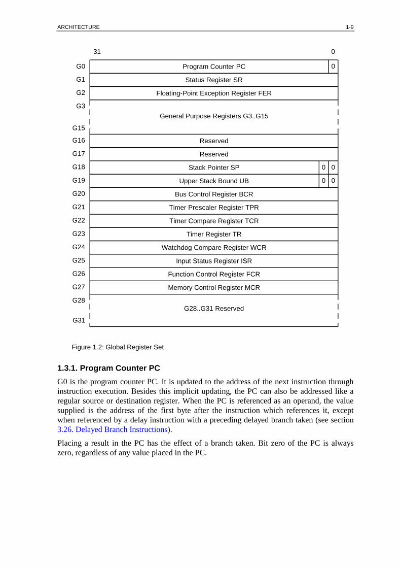
1.3. Global Register Set The architecture provides 32 global registers of 32 bits each. These are:
G0 Program Counter PC
G1 Status Register SR
G2 Floating-Point Exception Register FER
G3..G15 General purpose registers
G16..G17 Reserved
G18 Stack Pointer SP
G19 Upper Stack Bound UB
G20 Bus Control Register BCR (see section 6. Bus Interface)
G21 Timer Prescaler Register TPR (see section 5. Timer)
G22 Timer Compare Register TCR (see section 5. Timer and CPU Clock Modes)
G23 Timer Register TR (see section 5. Timer and CPU Clock Modes)
G24 Watchdog Compare Register WCR (see section 6. Bus Interface)
G25 Input Status Register ISR (see section 6. Bus Interface)
G26 Function Control Register FCR (see section 6. Bus Interface)
G27 Memory Control Register MCR (see section 6. Bus Interface)
G28..G31 Reserved
Registers G0..G15 can be addressed directly by the register code (0..15) of an instruction. Registers G18..G27 can be addressed only by a MOV or MOVI instruction with the high global flag H set to 1.
ARCHITECTURE 1-9
G0
031
0
G1
G2
G3
G15
G16
G17
G18
G19
G20
G21
G22
G23
G24
G25
G26
G27
Program Counter PC
Status Register SR
Floating-Point Exception Register FER
Reserved
Reserved
General Purpose Registers G3..G15
Stack Pointer SP
Upper Stack Bound UB
Bus Control Register BCR
Timer Prescaler Register TPR
Timer Compare Register TCR
Timer Register TR
Watchdog Compare Register WCR
Input Status Register ISR
Function Control Register FCR
Memory Control Register MCR
G28..G31 Reserved
0
00
0
G28
G31
Figure 1.2: Global Register Set
1.3.1. Program Counter PC G0 is the program counter PC. It is updated to the address of the next instruction through instruction execution. Besides this implicit updating, the PC can also be addressed like a regular source or destination register. When the PC is referenced as an operand, the value supplied is the address of the first byte after the instruction which references it, except when referenced by a delay instruction with a preceding delayed branch taken (see section 3.26. Delayed Branch Instructions).
Placing a result in the PC has the effect of a branch taken. Bit zero of the PC is always zero, regardless of any value placed in the PC.

1-10 CHAPTER 1
1.3.2. Status Register SR G1 is the status register SR. Its content is updated by instruction execution. Besides this implicit updating, the SR can also be addressed like a regular register. When addressed as source or destination operand, all 32 bits are used as an operand. However, only bits 15..0 of a result can be placed in bits 15..0 of the SR, bits 31..16 of the result are discarded and bits 31..16 of the SR remain unchanged. The full content of the SR is replaced only by the Return Instruction. A result placed in the SR overrules any setting or clearing of the condi-tion flags as a result of an instruction.
Frame Pointer Frame Length
2829
FL S P T
Trace-Mode FlagTrace Pending Flag
Supervisor State Flag
Instruction-Length Code
31 30 27 26 25 24 23 22 21 20 19 18 17 16
ILCFP
Figure 1.3: Status Register SR (bits 31..16)
Floating-Point Rounding ModeFloating-Point Trap Enable
Interrupt-Mode Flag
High Global FlagCache-Mode Flag
1213
FTE V N Z C
Carry FlagZero Flag
Negative Flag
Overflow Flag
15 14 11 10 9 8 7 6 5 4 3 2 1 0
MHFRML I
Reserved
Interrupt-Lock Flag
Figure 1.4: Status Register SR (bits 15..0)
ARCHITECTURE 1-11
1.3.2. Status Register SR (continued) The status register SR contains the following status information:
C Bit zero is the carry condition flag C. In general, when set it indicates that the unsigned integer range has been exceeded. At add operations, it indicates a carry out of bit 31 of the result. At subtract operations, it indicates a borrow (inverse carry) into bit 31 of the result.
Z Bit one is the zero condition flag Z. When set, it indicates that all 32 or 64 re-sult bits are equal to zero regardless of any carry, borrow or overflow.
N Bit two is the negative condition flag N. On compare instructions, it indicates the arithmetic correct (true) sign of the result regardless of an overflow. On all other instructions, it is derived from result bit 31, which is the true sign bit when no overflow occurs. In the case of overflow, result bit 31 and N reflect the inversion of the true sign.
V Bit three is the overflow condition flag V. In general, when set it indicates a signed overflow.
M Bit four is the cache-mode flag M. Besides being set or cleared under program control, it is also automatically cleared by a Frame instruction and by any branch taken except a delayed branch. See section 1.9. Instruction Cache for details.
H Bit five is the high global flag H. When H is set, denotation of G0..G15 addres-ses G16..G31 instead. Thus, the registers G18..G27 may be addressed by deno-ting G2..G11 respectively. The H flag is effective only in the first cycle of the next instruction after it was set; then it is cleared automatically. Only the MOV or MOVI instruction issued as the next instructions can be used to copy the content of a local register or an immediate value to one of the high global registers. The MOV instruction can also be used to copy the content of a high global register (except the BCR, TPR, FCR and MCR register, which are write-only) to a local register. With all other instructions, the result may be in-valid. If one of the high global registers is addressed as the destination register in user state (S = 0), the condition flags are undefined, the destination register remains unchanged and a trap to Privilege Error occurs.
Reserved Bit six is reserved for future use. It must always be zero.
I Bit seven is the interrupt-mode flag I. It is set automatically on interrupt entry and reset to its old value by a Return instruction. The I flag is used by the oper-ating system; it must be never changed by any user program, regardless of user or supervisor state.
FTE Bits 12..8 are the floating-point trap enable flags (see section 3.33.2. Floating-Point Instructions).
FRM Bits 14..13 are the floating-point rounding modes (see section 3.33.2. Floating-Point Instructions).
1-12 CHAPTER 1
1.3.2. Status Register SR (continued) L Bit 15 is the interrupt-lock flag L. When the L flag is one, all Interrupt, Parity
Error and Extended Overflow exceptions regardless of individual mode bits are inhibited. The state of the L flag is effective immediately after any instruction which changed it. The L flag is set to one by any exception. The L flag can be cleared or kept set in any or on return to any privilege state (user or supervisor). Changing the L flag from zero to one is privileged to su-pervisor or return from supervisor to supervisor state. A trap to Privilege Error occurs if the L flag is set under program control from zero to one in user or on return to user state.
The following status information cannot be changed by addressing the SR:
T Bit 16 is the trace-mode flag T. When both the T flag and the trace pending flag P are one, a trace exception occurs after every instruction except after a De-layed Branch instruction. The T flag is cleared by any exception. Note: The T flag can only be changed in the saved return SR and is then effec-tive after execution of a Return instruction.
P Bit 17 is the trace pending flag P. It is automatically set to one by all in-structions except by the Return instruction, which restores the P flag from bit 17 of the saved return SR. Since for a Trace exception both the P and the T flag must be one, the P flag determines whether a trace exception occurs (P = 1) or does not occur (P = 0) immediately after a Return instruction which restored the T flag to one. Note: The P flag can only be changed in the saved SR. No program except the trace exception handler should affect the saved P flag. The trace exception han-dler must clear the saved P flag to prevent a trace exception on return, in order to avoid tracing the same instruction in an endless loop.
S Bit 18 is the supervisor state flag S (see section 1.5. Privilege States). It is set to one by any exception.
ILC Bits 20 and 19 represent the instruction-length code ILC. It is updated by in-struction execution. The ILC holds (in general) the length of the last in-struction: ILC values of one, two or three represent an instruction length of one, two or three half-words respectively. After a branch taken, the ILC is invalid. The Return instruction clears the ILC. Note: Since a Return instruction following an exception clears the ILC, a pro-gram must not rely on the current value of the ILC.
FL Bits 24..21 represent the frame length FL. The FL holds the number of usable local registers (maximum 16) assigned to the current stack frame. FL = 0 is always interpreted as FL = 16.
FP Bits 31..25 represent the frame pointer FP. The least significant six bits of the FP point to the beginning of the current stack frame in the local register set, that is, they point to L0. The FP contains bit 8..2 of the address at which the content of L0 would be stored if pushed onto the memory part of the stack.
ARCHITECTURE 1-13
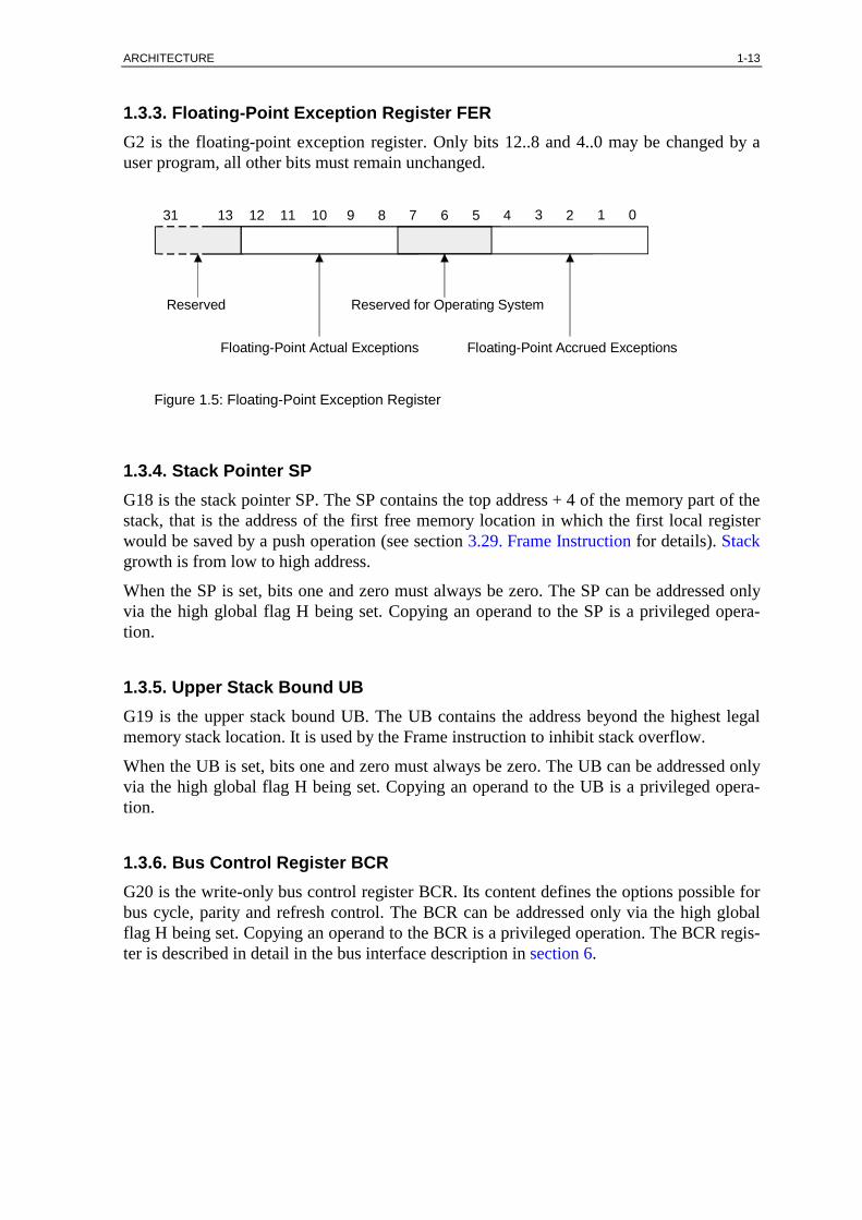
1.3.3. Floating-Point Exception Register FER G2 is the floating-point exception register. Only bits 12..8 and 4..0 may be changed by a user program, all other bits must remain unchanged.
Reserved
Floating-Point Actual Exceptions
Reserved for Operating System
Floating-Point Accrued Exceptions
1213 11 10 9 8 7 6 5 4 3 2 1 031
Figure 1.5: Floating-Point Exception Register
1.3.4. Stack Pointer SP G18 is the stack pointer SP. The SP contains the top address + 4 of the memory part of the stack, that is the address of the first free memory location in which the first local register would be saved by a push operation (see section 3.29. Frame Instruction for details). Stack growth is from low to high address.
When the SP is set, bits one and zero must always be zero. The SP can be addressed only via the high global flag H being set. Copying an operand to the SP is a privileged opera-tion.
1.3.5. Upper Stack Bound UB G19 is the upper stack bound UB. The UB contains the address beyond the highest legal memory stack location. It is used by the Frame instruction to inhibit stack overflow.
When the UB is set, bits one and zero must always be zero. The UB can be addressed only via the high global flag H being set. Copying an operand to the UB is a privileged opera-tion.
1.3.6. Bus Control Register BCR G20 is the write-only bus control register BCR. Its content defines the options possible for bus cycle, parity and refresh control. The BCR can be addressed only via the high global flag H being set. Copying an operand to the BCR is a privileged operation. The BCR regis-ter is described in detail in the bus interface description in section 6.
1-14 CHAPTER 1
1.3.7. Timer Prescaler Register TPR G21 is the write-only timer prescaler register TPR. It adapts the timer clock to different processor clock frequencies and controls the processor clock generation by the PLL circuit. The TPR can be addressed only via the high global flag H being set. Copying an operand to the TPR is a privileged operation. The TPR is described in the timer description in section 5. Updating TPR with amended values for the PLL multiplication factor in conjunction with corresponding updated values for the timer prescaler changes the internal clock fre-quency while keeping all timer settings correct.
1.3.8. Timer Compare Register TCR G22 is the timer compare register TCR. Its content is compared continuously with the con-tent of the timer register TR. The TCR can be addressed only via the high global flag H being set. Copying an operand to the TCR is a privileged operation. The TCR is described in the timer description in section 5.
1.3.9. Timer Register TR G23 is the timer register TR. Its content is incremented by one on each time unit. The TR can be addressed only via the high global flag H being set. Copying an operand to the TR is a privileged operation. The TR is described in the timer description in section 5.
1.3.10. Watchdog Compare Register WCR G24 is the watchdog compare register WCR. The WCR can be addressed only via the high global flag H being set. Copying an operand to the WCR is a privileged operation. The WCR is described in the bus interface description in section 6.
1.3.11. Input Status Register ISR G25 is the read-only input status register ISR. The ISR can be addressed only via the high global flag H being set. The ISR is described in the bus interface description in section 6.
1.3.12. Function Control Register FCR G26 is the write-only function control register FCR. The FCR can be addressed only via the high global flag H being set. Copying an operand to the FCR is a privileged operation. The FCR is described in the bus interface description in section 6.
1.3.13. Memory Control Register MCR G27 is the write-only memory control register MCR. The MCR can be addressed only via the high global flag H being set. Copying an operand to the MCR is a privileged operation. The MCR is described in the bus interface description in section 6.
ARCHITECTURE 1-15
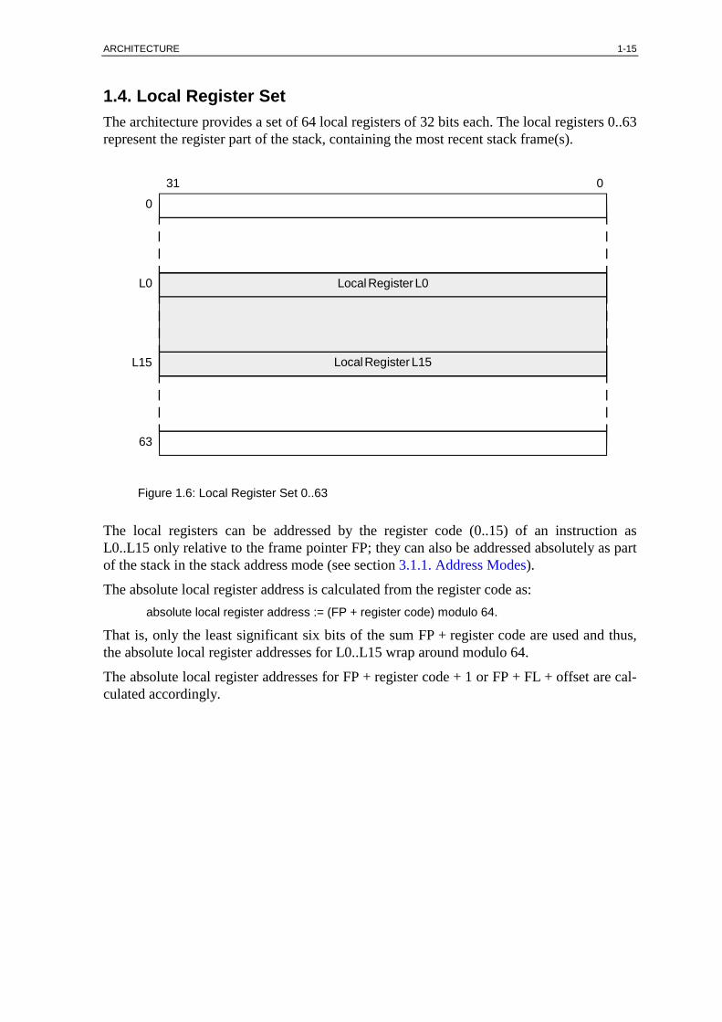
1.4. Local Register Set The architecture provides a set of 64 local registers of 32 bits each. The local registers 0..63 represent the register part of the stack, containing the most recent stack frame(s).
0
Local Register L0
Local Register L15
310
L0
L15
63
Figure 1.6: Local Register Set 0..63
The local registers can be addressed by the register code (0..15) of an instruction as L0..L15 only relative to the frame pointer FP; they can also be addressed absolutely as part of the stack in the stack address mode (see section 3.1.1. Address Modes).
The absolute local register address is calculated from the register code as: absolute local register address := (FP + register code) modulo 64.
That is, only the least significant six bits of the sum FP + register code are used and thus, the absolute local register addresses for L0..L15 wrap around modulo 64.
The absolute local register addresses for FP + register code + 1 or FP + FL + offset are cal-culated accordingly.

1-16 CHAPTER 1
1.5. Privilege States The architecture provides two privilege states, determined by the supervisor state flag S: user state (S = 0) and supervisor state (S = 1).
The runtime kernel hyRTK is executed in the higher privileged supervisor state, thereby restricting access to all sensitive data to a highly reliable system program. The following operations are also privileged to be executed only in the supervisor or on return from su-pervisor to supervisor state:
Copying an operand to any of the high global registers
Changing the interrupt-lock flag L from zero to one
Returning through a Return instruction to supervisor state
Any illegal attempt causes a trap to Privilege Error.
The S flag is also saved in bit zero of the saved return PC by the Call, Trap and Software instructions and by an exception. A Return instruction restores it from this bit position to the S flag in bit position 18 of the SR (thereby overwriting the bit 18 returned from the saved return SR).
If a Return instruction attempts a return from user to supervisor state, a trap to Privilege Error occurs (S = 1 is saved).
Returning from supervisor to user state is achieved by clearing the S flag in bit zero of the saved return PC before return. Switching from user to supervisor state is only possible by executing a Trap instruction or by exception processing through one of the 64 supervisor subprogram entries (see section 2.4. Entry Tables).

ARCHITECTURE 1-17
1.6. Register Data Types
32 Bits
Bitstring
31
MSB LSB
0
S = sign bit, MSB = most significant bit, LSB = least significant bit
Double-Word Bitstring
32-Bit Magnitude
Unsigned Integer
31
MSB LSB
Unsigned Double-Word Integer
31-Bit Magnitude
Signed Integer, Two's Complement
31
MSB LSBS
High-Order 31-Bit Magnitude
Signed Double-Word Integer, Two's Complement
31
LSBLow-Order 32-Bit Magnitude
MSBS
23-Bit Fraction
Single Precision Floating-Point Number
31
MSB LSB
0
S 8-Bit Exponent
High-Order 20-Bit Fraction
Double Precision Floating-Point Number
31
LSB
0
Low-Order 32-Bit Fraction
11-Bit ExponentS MSB
Register:
Complex Signed Short
31
MSB LSB
0
S MSB LSB S
Two Signed Shorts
31
MSB LSB
0
S MSB LSB S
15
15
Real Part Imaginary Part
High-Order 32-Bit Magnitude
31
LSBLow-Order 32-Bit Magnitude
MSB
High-Order 32-Bits
LSBLow-Order 32-Bits
MSB
n+1
n
n
n
0
n
n
n+1
0
n
n
n+1
n
n+1
n
n
0
0
31 0
Figure 1.7: Register Data Types

1-18 CHAPTER 1
1.7. Memory Organization The architecture provides a memory address space in the range of 0..232 - 1 (0..4 294 967 295) 8-bit bytes. Memory is implied to be organized as 32-bit words. The fol-lowing memory data types are available (see figure 1.8)
Byte unsigned (unsigned 8-bit integer, bit string or character)
Byte signed (signed 8-bit integer, two's complement)
Half-word unsigned (unsigned 16-bit integer or bit string)
Half-word signed (signed 16-bit integer, two's complement)
Word (32-bit undedicated word)
Double-word (64-bit undedicated double-word)
Besides the memory address space, a separate I/O address space is provided. In the I/O ad-dress space, only word and double-word data types are available.
Words and double-words must be located at word boundaries, that is, their most significant byte must be located at an address whose two least significant bits are zero. Half-words must be located at half-word boundaries, their most significant byte being located at an address whose least significant bit is zero. Bytes may be located at any address.
The variable-length instructions are located as contiguous sequences of one, two or three half-words at half-word boundaries.
Memory- and I/O-accesses are pipelined to a depth of two words.
Note: All data is located high to low order at addresses ascending from low to high, that is, the high order part of all data is located at the lower address (big-endian).
ARCHITECTURE 1-19
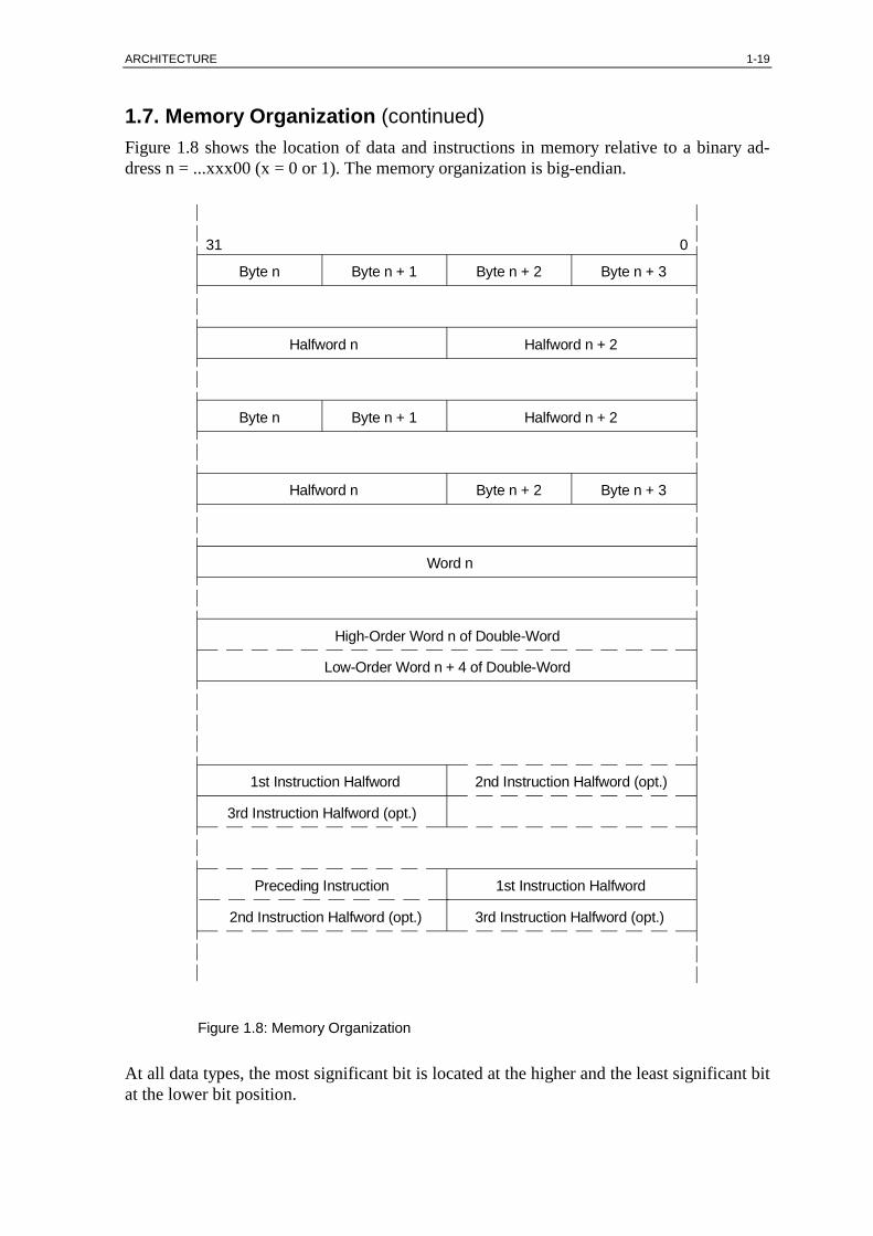
1.7. Memory Organization (continued) Figure 1.8 shows the location of data and instructions in memory relative to a binary ad-dress n = ...xxx00 (x = 0 or 1). The memory organization is big-endian.
31
Byte n Byte n + 1 Byte n + 2 Byte n + 3
0
Halfword n Halfword n + 2
Byte n Byte n + 1 Halfword n + 2
Halfword n Byte n + 2 Byte n + 3
Word n
High-Order Word n of Double-Word
Low-Order Word n + 4 of Double-Word
1st Instruction Halfword 2nd Instruction Halfword (opt.)
3rd Instruction Halfword (opt.)
Preceding Instruction 1st Instruction Halfword
2nd Instruction Halfword (opt.) 3rd Instruction Halfword (opt.)
Figure 1.8: Memory Organization
At all data types, the most significant bit is located at the higher and the least significant bit at the lower bit position.

1-20 CHAPTER 1
1.8. Stack A runtime stack, called stack here, holds generations of local variables in last-in-first-out order. A generation of local variables, called stack frame or activation record, is created upon subprogram entry and released upon subprogram return.
The runtime stack provided by the architecture is divided into a memory part and a register part. The register part of the stack, implemented by a set of 64 local registers organized as a circular buffer, holds the most recent stack frame(s). The current stack frame is always kept in the register part of the stack. The frame pointer FP points to the beginning of the current stack frame (addressed as register L0). The frame length FL indicates the number of regis-ters (maximum 16) assigned to the current stack frame. The stack grows from low to high address. It is guarded by the upper stack bound UB.
The stack is maintained as follows:
A Call, Trap or Software instruction increments the FP and sets FL to six, thus creating a new stack frame with a length of six registers (including the return PC and the return SR).
An exception increments the FP by the value of FL and then sets FL to two.
A Frame instruction restructures a stack frame to include (optionally) passed parameters by decrementing the FP and by resetting the FL to the desired length, and restores a re-serve of 10 local registers for the next subprogram call. If the required number of regis-ters + 10 do not fit in the register part of the stack, the contents of the differential (re-quired + 10 - available) number of local registers are pushed onto the memory part of the stack. A trap to Frame Error occurs after the push operation when the old value of the stack pointer SP exceeded the upper stack bound UB.
A Return instruction releases the current stack frame and restores the preceding stack frame. If the restored stack frame is not fully contained in the register part of the stack, the content of the missing part of the stack frame is pulled from the memory part of the stack.
For more details see the descriptions of the specific instructions.
When the number of local registers required for a stack frame exceeds its maximum length of 16 (in rare cases), a second runtime stack in memory may be used. This second stack is also required to hold local record or array data.
The stack is used by routines in user or supervisor state, that is, supervisor stack frames are appended to user stack frames, and thus, parameters can be passed between user and super-visor state. A small stack space must be reserved above UB. UB can then be set to a higher value by the Frame Error handler to free stack space for error handling.

ARCHITECTURE 1-21
1.8. Stack (continued) Because the complete stack management is accomplished automatically by the hardware, programming the stack handling instructions is easy and does not require any knowledge of the internal working of the stack.
The following example demonstrates how the Call, Frame and Return instructions are ap-plied to achieve the stack behavior of the register part of the stack shown in the figures 1.9 and 1.10.
A currently activated function A has a frame length of FL = 13. Registers L0..L6 are to be retained through a subsequent call, registers L7..L12 are temporaries. A call to function B needs 2 parameters to be passed. The parameters are placed by function A in registers L7 and L8 before calling B. The Call instruction addresses L9 as destination for the return PC and return SR register pair to be used by function B on return to function A.
On entry of function B, the new frame of B has an implicit length of FL = 6. It starts physi-cally at the former register L9 of frame A. However, since the frame pointer FP has been incremented by 9 by the Call instruction, this register location is now being addressed as L0 of frame B. The passed parameters cannot be addressed because they are located below the new register L0 of frame B. To make them addressable, a Frame instruction decrements the frame pointer FP by 2. Then, parameter 1 and 2 passed to B can be addressed as regis-ters L0 and L1 respectively. Note that the return PC is now to be addressed as L2!
The Frame instruction in B specifies also the new, complete frame length FL = 11 (includ-ing the passed parameters as well as the return PC and return SR pair). Besides, a new re-serve of 10 registers for subsequent function calls and traps is provided in the register stack. A possible overflow of the register stack is checked and handled automatically by the Frame instruction. A program needs not and must not pay attention to register stack over-flow.
At the end of function B, a Return instruction returns control to function A and restores the frame A. A possible underflow of the register stack is handled also automatically; thus, the frame A is always completely restored, regardless whether it was wholly or partly pushed into the memory part of the stack before (in the case when B called other functions).
In the present example with the frame length of FL = 13, any suitable destination register up to L13 could be specified in the Call instruction. The parameters to be passed to the function B would then be placed in L11 and L12. It is even possible to append a new frame to a frame with a length of FL = 16 (coded as FL = 0 in the status register SR): the destina-tion register in the Call instruction is then coded as L0, but interpreted as the register past L15.
See also sections 3.27. Call instruction, 3.29. Frame instruction and 3.30. Return instruc-tion for further details.
Note: With an average frame length of 8 registers, ca. 7..8 Frame instructions succeed a pulling Return instruction until a push occurs and 7..8 Return instructions succeed a push-ing Frame instruction until a pull occurs. Thus, the built-in hysteresis makes pushing and pulling a rare event in regular programs.

1-22 CHAPTER 1
1.8. Stack (continued) Program Example:
A: FRAME L13, L3 ; set frame length FL = 13, decrement FP by 3 : ; parameters passed to A can be addressed : ; in L0, L1, L2 : : code of function A : : MOV L7, L5 ; copy L5 to L7 for use as parameter1 MOVI L8, 4 ; set L8 = 4 for use as parameter2 CALL L9, 0, B ; call function B, : ; save return PC, return SR in L9, L10 : : MOVI L0, 20 ; set L0 = 20 as return parameter for caller RET PC, L3 ; return to function calling A, ; restore frame of caller
B: FRAME L11, L2 ; set frame length FL = 11, decrement FP by 2 : ; passed parameter1 can now be addressed in L0 : ; passed parameter2 can now be addressed in L1 : : code of function B : : RET PC, L2 ; return to function A, frame A is restored by ; copying return PC and return SR in L2 and L3 ; of frame B to PC and SR

ARCHITECTURE 1-23
1.8. Stack (continued) Figure 1.9 shows the creation and release of stack frames in the register part of the stack.
Return from B Call B Frame in B
PC := ret. PC for B; PC := branch address; FP := FP - code of source reg.; SR := ret. SR for B; ret. PC for B := old PC; FL := code of dest.reg.; -- returns preceding stack frame ret. SR for B := old SR; if available registers ≥ if stack frame contained FP := FP + reg.code (required + 10) registers then in local registers then of ret. PC; next instruction next instruction; FL := 6; else else -- reg.code of ret. PC = 9 push contents of pull contents of differential words differential number of from memory part of the stack; registers to memory part of stack; -- code of source reg. = 2 -- code of dest.reg. = 11
L0L1L2L3L4L5L6L7L8L9L10L11L12L13L14L15
FramePointer(FP)
currentlengthof frame AFL = 13
parametersfor
must notbe usedFP+FL
L0L1L2L3L4L5
NewFP
currentlengthof frame BFL = 6
parametersfor frame B
ret. PC for Aret. SR for A
reservedfor
maximumnumber ofvariables
in frame A
ret. PC for Bret. SR for B
FP+FL
reserved formax. numberof variablesin frame B
parametersfor
ret. PC for Aret. SR for A
NewFP
currentlengthof frame BFL = 11
parametersfor frame B
ret. PC for Bret. SR for B
FP+FL
parametersfor
ret. PC for Aret. SR for A
reservedfor
maximumnumber ofvariables
in frame B
L0L1L2L3L4L5L6L7L8L9L10
frame A frame A frame A
before Call and after CALL L9, 0, dest; after FRAME L11, L2 after Return
Figure 1.9: Stack frame handling (register part)
1-24 CHAPTER 1
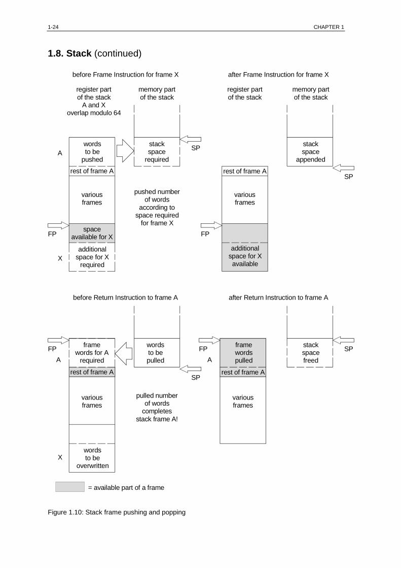
1.8. Stack (continued)
register partof the stack
A and Xoverlap modulo 64
memory part of the stack
register partof the stack
memory partof the stack
before Frame Instruction for frame X after Frame Instruction for frame X
Awordsto be
pushed
Xadditional
space for Xrequired
pushed numberof words
according tospace required
for frame X
stackspace
appended
before Return Instruction to frame A after Return Instruction to frame A
framewords for A
required
wordsto be
overwritten
words to be pulled
pulled numberof words
completesstack frame A!
framewordspulled
stackspacefreed
FP
SP
FP
additionalspace for Xavailable
SP
A
X
FP
SP
SPFP
stackspace
requiredrest of frame A
variousframes
variousframes
rest of frame A
spaceavailable for X
rest of frame A
variousframes
A
rest of frame A
variousframes
= available part of a frame
Figure 1.10: Stack frame pushing and popping

ARCHITECTURE 1-25
1.9. Instruction Cache The instruction cache is transparent to programs. A program executes correctly even if it ignores the cache, whereby it is assumed that a program does not modify the instruction code in the local range contained in the cache.
The instruction cache holds a total of up to 128 bytes (32 unstructured 32-bit words of in-structions). It is implemented as a circular buffer which is guarded by a look-ahead counter and a look-back counter. The look-ahead counter holds the highest and the look-back counter the lowest address of the instruction words available in the cache. The cache-mode flag M is used to optimize special cases in loops (see details below). The cache can be re-garded as a temporary local window into the instruction sequence, moving along with in-struction execution and being halted by the execution of a program loop.
Its function is as follows:
The prefetch control loads unstructured 32-bit instruction words (without regard to instruc-tion boundaries) from memory into the cache. The load operation is pipelined to a depth of two stages (see section 3.1. Memory Instructions for details of the load pipeline). The look-ahead counter is incremented by four at each prefetch cycle. It always contains the address of the last instruction word for which an address bus cycle is initiated, regardless of whether the addressed instruction word is in the load pipeline or already loaded into the instruction cache.
The prefetched instruction word is placed in the cache word location addressed by bits 6..2 of the look-ahead counter. The look-back counter remains unchanged during prefetch un-less the cache word location it addresses with its bits 6..2 is overwritten by a prefetched instruction word. In this case, it is incremented by four to point to the then lowest-addressed usable instruction word in the cache. Since the cache is implemented as a circu-lar buffer, the cache word addresses derived from bits 6..2 of the look-ahead and look-back counter wrap around modulo 32.
The prefetch is halted:
When eight words are prefetched, that is, eight words are available (including those pending in the load pipeline) in the prefetch sequence succeeding the instruction word addressed by the program counter PC through the instruction word addressed by the look-ahead counter. Prefetch is resumed when the PC is advanced by instruction execu-tion.
In the cycle preceding the execution cycle of an instruction accessing memory or I/O or any potentially branch-causing instruction (regardless of whether the branch is taken) except a forward Branch or Delayed Branch instruction with an instruction length of one half-word and a branch target contained in the cache. Halting the prefetch in these cases avoids filling the load pipeline with demands for potentially unnecessary instruction words. The prefetch is also halted during the execution cycle of any instruction acces-sing memory or I/O.
1-26 CHAPTER 1
1.9. Instruction Cache (continued) The cache is read in the decode cycle by using bits 6..1 of the PC as an address to the first half-word of the instruction presently being decoded. The instruction decode needs and uses only the number (1, 2 or 3) of instruction half-words defined by the instruction format. Since only the bits 6..1 of the PC are used for addressing, the half-word addresses wrap around modulo 64. Idle wait cycles are inserted when the instruction is not or not fully available in the cache.
At an explicit Branch or Delayed Branch instruction (except when placed as delay instruc-tion) with an instruction length of one half-word, the location of the branch target is checked. The branch target is treated as being in the cache when the target address of a backward branch is not lower than the address in the look-back counter and the target ad-dress of a forward branch is not higher than two words above the address in the look-ahead counter. That is, the two instruction words succeeding the instruction word addressed by the content of the look-ahead counter are treated by a forward branch as being in the cache. Their actual fetch overlaps in most cases with the execution of the branch instruction and thus, no cycles are wasted. When the branch target is in the cache, the look-back counter and the look-ahead counter remain unchanged.
When a branch is taken by a Delayed Branch instruction with an instruction length of one half-word to a forward branch target not in the cache and the cache mode flag M is enabled (1), the look-back counter and the look-ahead counter remain unchanged. Wait cycles are then inserted until the ongoing prefetch has loaded the branch target instruction into the cache.
Any other branch taken flushes the cache by placing the branch address in the look-back and the look-ahead counter. Prefetch then starts immediately at the branch address. Instruc-tion decoding waits until the branch target instruction is fully available in the cache.
The cache mode flag M (bit four of the SR) can be set or cleared by logical instructions. It is automatically cleared by a Frame instruction and by any branch taken except a branch caused by a Delayed Branch or Return instruction; a Delayed Branch instruction leaves the M flag unchanged and a Return instruction restores the M flag from the saved status regis-ter SR.
Note: Since up to eight instruction words can be loaded into the cache by the prefetch, only 24 instruction words are left to be contained in a program loop. Thus, a program loop can have a maximum length of 96 or 94 bytes including the branch instruction closing the loop, depending on the even or odd half-word address location of the first instruction of the loop respectively.
A forward Branch or Delayed Branch instruction with an instruction length of one half-word into up to two instruction words succeeding the word addressed by the look-ahead counter treats the branch target as being in the cache and does not flush the cache. Thus, three or four instruction half-words, depending on the odd or even half-word address loca-tion of the branch instruction respectively, can always be skipped without flushing the cache.
ARCHITECTURE 1-27
1.9. Instruction Cache (continued) Enabling the cache-mode flag M is only required when a program loop to be contained in the cache contains a forward branch to a branch target in the program loop and more than three (or four, see above) instruction half-words are to be skipped. In this case, the enabled M flag in combination with a Delayed Branch instruction with an instruction length of one half-word inhibits flushing the cache when the branch target is not yet prefetched.
Since a single-word memory instruction halts the prefetch for two cycles, any sequence of memory instructions, even with interspersed one-cycle non-memory instructions, halts the prefetch during its execution. Thus, alternating between instruction and data memory pages is avoided. If the number of instruction half-words required by such a sequence is not guar-anteed to be in the cache at the beginning of the sequence, a Fetch instruction enforcing the prefetch of the sequence may be used. A Fetch instruction may also be used preceding a branch into a program loop; thus, flushing the cache by the first branch repeating the loop can be avoided.
A branch taken caused by a Branch or Delayed Branch instruction with an instruction length of two half-words always flushes the instruction cache, even if the branch target is in the cache. Thus, branches can be forced to bypass the cache, thereby reducing the cache to a prefetch buffer. This reduced function can be used for testing.
1.10. On-Chip Memory (IRAM) 16 KBytes of memory are provided on-chip. The on-chip memory (IRAM) is mapped to the hex address C000 0000 of the memory address space and wraps around modulo 16K up to DFFF FFFF. The IRAM is implemented as a fully static memory block.
An access to the IRAM bypasses the access pipeline of the external memory. Thus, pend-ing external memory accesses do not delay accesses to the IRAM. The IRAM can hold data as well as instructions. Instruction words from the IRAM are automatically transferred to the instruction cache on demand; these transfers do not interfere with external memory accesses. Besides bypassing of the external memory pipeline, memory instructions access-ing the IRAM behave exactly alike those accessing external memory. The minimum delay for a load access is one cycle; that is, the data is not available in the cycle after the load instruction. One or more wait cycles are automatically inserted if the target register of the load is addressed before the data is loaded into the target register.
Attention: For selection between an internal and external memory access, bits 31..29 of the specified address register are used before calculation of the effective address. Therefore, the content of the specified address register must point into the IRAM address range. The IRAM address range boundary must not be crossed when the effective memory address is calculated in the displacement address mode.

1-28 CHAPTER 1
This page is intentionally left blank.
INSTRUCTIONS GENERAL 2-1
2. Instructions General
2.1. Instruction NotationIn the following instruction-set presentation, an informal description of an instruction isfollowed by a formal description in the form:
Format Notation Operation
Format denotes the instruction format.
Notation gives the assembler notation of the instruction.
Operation describes the operation with the following symbols:
Ls denotes any of the local registers L0..L15 used as source register or as source oper-and. At memory Load instructions, Ls denotes the load destination register.
Ld denotes any of the local registers L0..L15 used as destination register or as destina-tion operand.
Rs denotes any of the local registers L0..L15 or any of the global registers G0..G15used as source register or as source operand. At memory Load instructions, Rs de-notes the load destination register.
Rd denotes any of the local registers L0..L15 or any of the global registers G0..G15used as destination register or as destination operand.
Lsf, Ldf, Rsf and Rdf denote the register or operand following after (with a register addressone higher than) Ls, Ld, Rs and Rd respectively.
imm, const, dis, lim, rel, adr and n denote immediate operands (constants) of various for-mats and ranges.
Operand(x) denotes a single bit at the bit position x of an operand.Example: Ld(31) denotes bit 31 of Ld.
Operand(x..y) denotes bits x through y of an operand.Example: Ls(4..0) denotes bits 4 through 0 of Ls.
Expression^ denotes an operand at a location addressed by the value of the expression.Depending on the context, the expression addresses a memory location or a localregister.Example: Ld^ denotes a memory operand whose memory address is the operandLd. (FP + FL)^ denotes a local register operand whose register address is FP + FL.
:= signifies the assignment symbol, read as "is replaced by".
// signifies the concatenation symbol. It denotes concatenation of two operand wordsto a double-word operand or concatenation of bits and bitstrings.Examples: Ld//Ldf denotes a double-word operand, 16 zeros//imm1 denotes ex-panding of an immediate half-word by 16 leading zeros.
=, ≠, > and < denote the equal, unequal, greater than and less than relations.Example: The relation Ld = 0 evaluates to one if Ld is equal to zero, otherwise itevaluates to zero.

2-2 CHAPTER 2
2.2. Instruction ExecutionOn instruction execution, all bits of the operands participate in the operations, except onthe Shift and Rotate instructions (whereat only the 5 least significant bits of the source op-erand are used) and except on the byte and half-word Store instructions.
Instructions are executed by a two-stage pipeline. In the first stage, the instruction isfetched from the instruction cache and decoded. In the second stage, the instruction is exe-cuted while the next instruction in the first stage is already decoded.
On register instructions executing in one or two cycles, the corresponding source and desti-nation operand words are read from their registers and evaluated in each cycle in whichthey are used. Then the result word is placed in the corresponding destination register in thesame cycle. Thus, on all single-word register instructions executing in one cycle, the sourceoperand register and the destination operand register may coincide without changing theeffect of the instruction. On all other instructions, the effect of a register coincidence de-pends on execution order and must be examined specifically for each such instruction.
The content of a source register remains unchanged unless it is used coincidentally as adestination register (except on memory Load instructions).
Some instructions set or clear condition flags according to the result and special conditionsoccuring during their execution. The conditions may be expressed by single bits, relationsor logical combinations of these. If a condition evaluates to one (true), the correspondingcondition flag is set to one, if it evaluates to zero (false), the corresponding condition flagis cleared to zero. If the conditions for a Range Error are met, a trap to Range Error occursafter the flags and the destination are updated.
All instructions may use the result and any flags updated by the preceding instruction. Atime penalty occurs only if the result of a memory Load instruction is not yet availablewhen needed as destination or source operand. In this case one or more (depending on thememory access time) idle wait cycles are enforced by a hardware interlock.
An instruction must not use any local register of the register sequence beginning with L0beyond the number of usable registers specified by the current value of the frame length FL(FL = 0 is interpreted as FL = 16). That is, the value of the corresponding register code(0..15) addressing a local register must be lower than the interpreted value of the FL (ex-cept with a Call or Frame instruction or some restricted cases). Otherwise, an exceptioncould overwrite the contents of such a register or the beginning of the register part of thestack at the SP could be overwritten without any warning when a result is placed in such aregister.
Double-word instructions denote the high-order word (at the lower address). The low-orderword adjacently following it (at the higher address) is implied.
"Old" denotes the state before the execution of an instruction.

INSTRUCTIONS GENERAL 2-3
2.3. Instruction FormatsInstructions have a length of one, two or three half-words and must be located on half-wordboundaries. The following formats are provided:
Format
LL
LR
RR
Ln
Rn
PCadr
PCrel
PCrel
OP-code Ld-code Ls-code
OP-code n Ld-code n
OP-Code d n Rd-code n
OP-code adr-byte
OP-code 0 low-rel S
OP-code 1 high-rel
low-rel S
915 8 7 4 3 0
10 915 8 7 4 3 0
915 8 7 4 3 0
15 8 7 0
Ls-code encodes L0..L15 for LsLd-code encodes L0..L15 for Ld
Rs-code encodes G0..G15 for RsRs-code encodes L0..L15 for RsLd-code encosed L0..L15 for Ld
Rs-code encodes G0..G15 for RsRs-code encodes L0..L15 for RsRd-code encodes G0..G15 for RdRd-code encodes L0..L15 for Rd
Ld-code encodes L0..L15 for LdBit 8//bits 3..0 encode n = 0..31
Rd-code encodes G0..G15 for RdRd-code encodes L0..L15 for RdBit 8//bits 3..0 encode n = 0..31
adr = 24 ones's//adr-byte(7..2)//00
sign bit of relrel = 9 S//high-rel//low-rel//0range -8 388 608..8 388 606
sign bit of relrel = 25 S//low-rel//0range -128..126
10 915 8 7 4 3 0
15 8 7 06 1
15 8 7 06 1
OP-Code d s Rd-code Rs-code
15 8 7 4 3 0
OP-code s Ld-code Rs-code
Configuration
S:
S:
d = 0:d = 1:n:
n:
s = 0:s = 1:d = 0:d = 1:
s = 0:s = 1:
LLext OP-code
OP-code extension
15 8Ld-code Ls-code7 4 3 0 Ls-code encodes L0..L15 for Ls
Ld-code encodes L0..L15 for LdOP-code extension encodes theEXTEND instructions
Table 2.1: Instruction Formats, Part 1

2-4 CHAPTER 2
2.3. Instruction Formats (continued)
Configuration
LRconst
RRconst
915 8 7 4 3 0 Rs-code encodes G0..G15 for RsRs-code encodes L0..L15 for RsLd-code encodes L0..L15 for LdSign bit of constconst = 18 S//const1range -16 384..16 383const = 2 S//const1//const2range -1 073 741 824..1 073 741 8
Rs-code encodes G0..G15 for RsRs-code encodes L0..L15 for RsRd-code encodes G0..G15 for RdRd-code encodes L0..L15 for RdSign bit of constconst = 18 S//const 1range -16 384..16 383const = 2 S//const1//const2range -1 073 741 824..1 073 741 8
Rd-code encodes G0..G15 for RdRd-code encodes L0..L15 for RdBit 8//bits 3..0 encode n = 0..31see Table 2.3. Encoding ofImmediate Values for encoding ofimm
10 915 8 7 4 3 0d
OP-code s Ld-code Rs-code
OP-code s Rd-code Rs-code
RRdis 10 915 8 7 4 3 0
dOP-code s Rd-code Rs-codeRs-code encodes G0..G15 for RsRs-code encodes L0..L15 for RsRd-code encodes G0..G15 for RdRd-code encodes L0..L15 for RdSign bit of disdis = 20 S//dis1range -4 096..4 095dis = 4 S//dis1//dis2range -268 435 456..268 435 455D-code, D13..D12 encode datatypes at memory instructions
10 915 8 7 4 3 0dOP-code n Rd-code n
10 915 8 7 4 3 0dOP-code s Rd-code Rs-code
Rs-code encodes G0..G15 for RsRs-code encodes L0..L15 for RsRd-code encodes G0..G15 for RdRd-code encodes L0..L15 for RdX-code, X14..X12 encode Indexinstructionslim = 20 zeros//lim1range 0..4 095lim = 4 zeros//lim1//lim2range 0..268 435 455
14
14
14
Rimm
RRlim
e S const1
const2
e const1
const2
e S
S
D D dis1
dis2
imm1
imm2
e X X X lim1
lim2
Format
s = 0:s = 1:
S:e = 0:
e = 1:
s = 0:s = 1:d = 0:d = 1:S:e = 0:
e = 1:
s = 0:s = 1:d = 0:d = 1:S:e = 0:
e = 1:
DD:
d = 0:d = 1:n:
s = 0:s = 1:d = 0:d = 1:XXX:
e = 0:
e = 1:
14
Table 2.2: Instruction Formats, Part 2

INSTRUCTIONS GENERAL 2-5
2.3.1. Table of Immediate Values
n immediate value imm Comment
0..16 0..16 at CMPBI, n = 0 encodes ANYBZat ADDI and ADDSI n = 0 encodes CZ
17 imm1//imm2 range = 0..232-1 or -231..231-1
18 16 zeros//imm1 range = 0..65 535
19 16 ones//imm1 range = -65 536..-1
20 32 bit 5 = 1, all other bits = 0
21 64 bit 6 = 1, all other bits = 0
22 128 bit 7 = 1, all other bits = 0
23 231 bit 31 = 1, all other bits = 0
24 -8
25 -7
26 -6
27 -5
28 -4
29 -3
30 -2
31 231-1 at CMPBI and ANDNIbit 31 = 0, all other bits = 1
31 -1 at all other instructions using imm
Table 2.3: Encoding of Immediate Values
Note: 231 provides clear, set and invert of the floating-point sign bit at ANDNI, ORI andXORI respectively.
231-1 provides a test for floating-point zero at CMPBI and extraction of the sign bit atANDNI.
See CMPBI for ANYBZ and ADDI, ADDSI for CZ.

2-6 CHAPTER 2
2.3.2. Table of Instruction Codes
CHK, C
HKZ,
NO
P
XM
x, X
Xx
CM
P
CM
PB
MO
VD, R
ET
MASK
MO
V
AND
N
DIV
U
SUM
ADD
OR
DIV
S
SUM
S
ADD
S
XO
R
SUBS
NEG
S
ADD
SI
XO
RI
SUB
NEG
ADD
I
OR
I
NO
T
AND
MO
VI
AND
NI
SUBC
ADD
C
CM
PI
CM
PBI
SHR
DI
SHR
DSHR
LDxx
.D/A
/IOD
/IOA
SHR
I
MU
LU
FSU
BFS
UBD
DBE BE
DBN
E
BNE
FAD
DD
FAD
D
DBN
VD
BV
BNV
BVLD
W.R
LDD
.R
SAR
DI
SAR
DSAR
LDxx
.N/S
SAR
I
MU
LS
FDIV
FDIV
D
DBS
E
BSE
DBH
T
BHT
FMU
LDFM
UL
DBN
CD
BC
BNC
BCLD
W.P
LDD
.P
SHLD
ISHLD
SHL
STx
x.D
/A/IO
D/IO
A
SHLI
SET
xx, S
ETA
DR, F
ETC
H
FCM
PUFC
MPU
D
DBL
E
BLE
DBG
T
BG
T
FCM
PDFC
MP
DBN
ND
BN
BNN
BNS
TW.R
STD
.R
RES
ERVE
DTE
STL
ZR
OL
STx
x.N
/S
RES
ERVE
D
MU
L EXT
END
DO
CAL
L
FCVTD
FCVT
FRAM
ED
BR BRS
TW.P
STD
.P
TRAPx
x, T
RAP
23
10
67
54
AB
98
DC
FE
OP-
code
Bits
11.
.8
0 1 2 3 4 5 6 7 8 9 A B C D E F
OP-
code
Bits
15.
.12
Table 2.4: Table of Instruction Codes

INSTRUCTIONS GENERAL 2-7
2.3.3. Table of Extended DSP Instruction CodesThe Extended DSP instructions are specified by a 16-bit OP-code extension succeeding theinstruction op-code for the EXTEND instruction. See section 3.32. Extended DSP Instruc-tions.
Instruction OP-code exten-sion (hex)
EMUL 0102
EMULU 0104
EMULS 0106
EMAC 010A
EMACD 010E
EMSUB 011A
EMSUBD 011E
EHMAC 002A
EHMACD 002E
EHCMULD 0046
EHCMACD 004E
EHCSUMD 0086
EHCFFTD 0096
EHCFFTSD 0296
Table 2.5: Extended DSP Instruction Codes

2-8 CHAPTER 2
2.4. Entry TablesSpacing of the entries for the Trap instructions and exceptions is four bytes. These entriesare intended to each contain an instruction branching to the associated function. The entriesfor the TRAPxx instructions are the same as for TRAP. Table 2.6 shows the trap entrieswhen the entry table is mapped to the end of memory area MEM3 (default after Reset):
Address (Hex) Entry Description
FFFF FF00 TRAP 0
FFFF FF04 TRAP 1
: :
FFFF FFC0 TRAP 48 IO2 Interrupt -- priority 15
FFFF FFC4 TRAP 49 IO1 Interrupt -- priority 14
FFFF FFC8 TRAP 50 INT4 Interrupt -- priority 13
FFFF FFCC TRAP 51 INT3 Interrupt -- priority 11
FFFF FFD0 TRAP 52 INT2 Interrupt -- priority 9
FFFF FFD4 TRAP 53 INT1 Interrupt -- priority 7
FFFF FFD8 TRAP 54 IO3 Interrupt -- priority 5
FFFF FFDC TRAP 55 Timer Interrupt -- priority selectable as 6, 8, 10, 12
FFFF FFE0 TRAP 56 Reserved -- priority 17 (lowest)
FFFF FFE4 TRAP 57 Trace Exception -- priority 16
FFFF FFE8 TRAP 58 Parity Error -- priority 4
FFFF FFEC TRAP 59 Extended Overflow -- priority 3
FFFF FFF0 TRAP 60 Range, Pointer, Frame and Privilege Error -- priority 2
FFFF FFF4 TRAP 61 Reserved -- priority 1
FFFF FFF8 TRAP 62 Reset -- priority 0 (highest)
FFFF FFFC TRAP 63 Error entry for instruction code of all ones
Table 2.6: Trap entry table mapped to the end of MEM3
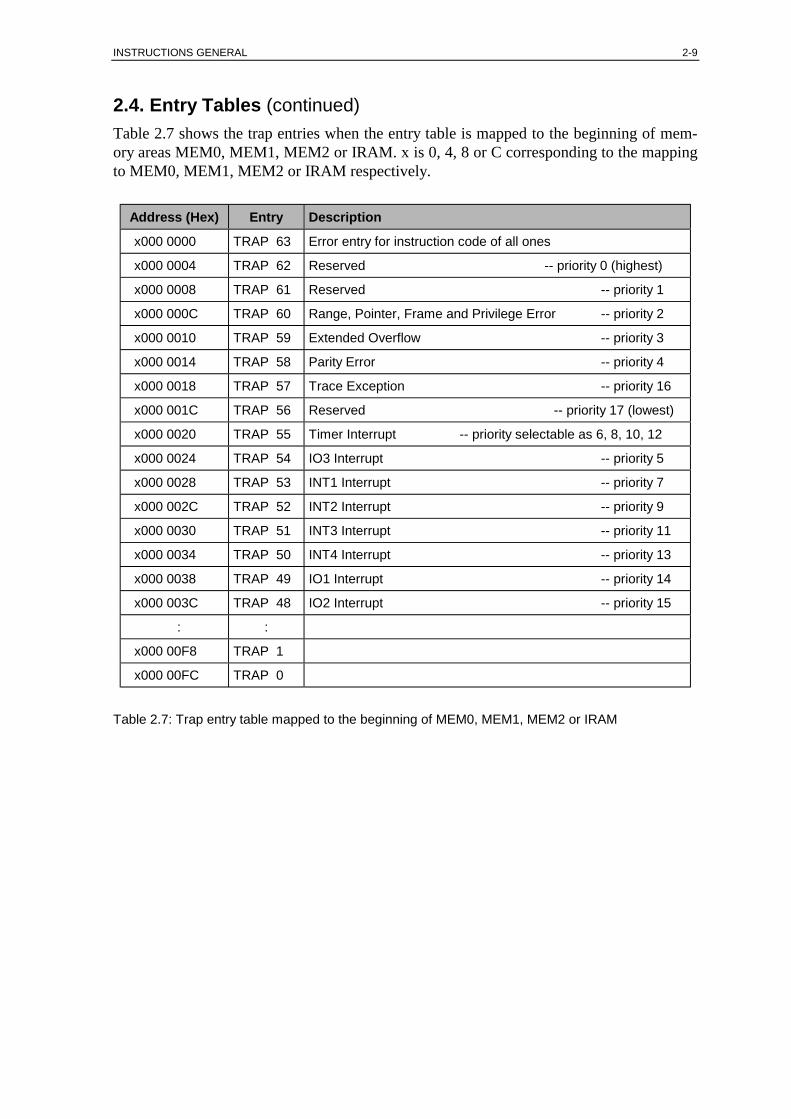
INSTRUCTIONS GENERAL 2-9
2.4. Entry Tables (continued)Table 2.7 shows the trap entries when the entry table is mapped to the beginning of mem-ory areas MEM0, MEM1, MEM2 or IRAM. x is 0, 4, 8 or C corresponding to the mappingto MEM0, MEM1, MEM2 or IRAM respectively.
Address (Hex) Entry Description
x000 0000 TRAP 63 Error entry for instruction code of all ones
x000 0004 TRAP 62 Reserved -- priority 0 (highest)
x000 0008 TRAP 61 Reserved -- priority 1
x000 000C TRAP 60 Range, Pointer, Frame and Privilege Error -- priority 2
x000 0010 TRAP 59 Extended Overflow -- priority 3
x000 0014 TRAP 58 Parity Error -- priority 4
x000 0018 TRAP 57 Trace Exception -- priority 16
x000 001C TRAP 56 Reserved -- priority 17 (lowest)
x000 0020 TRAP 55 Timer Interrupt -- priority selectable as 6, 8, 10, 12
x000 0024 TRAP 54 IO3 Interrupt -- priority 5
x000 0028 TRAP 53 INT1 Interrupt -- priority 7
x000 002C TRAP 52 INT2 Interrupt -- priority 9
x000 0030 TRAP 51 INT3 Interrupt -- priority 11
x000 0034 TRAP 50 INT4 Interrupt -- priority 13
x000 0038 TRAP 49 IO1 Interrupt -- priority 14
x000 003C TRAP 48 IO2 Interrupt -- priority 15
: :
x000 00F8 TRAP 1
x000 00FC TRAP 0
Table 2.7: Trap entry table mapped to the beginning of MEM0, MEM1, MEM2 or IRAM

2-10 CHAPTER 2
2.4. Entry Tables (continued)Table 2.8 below shows the addresses of the first instruction of the emulator code associatedwith the floating-point instructions when the trap entry tables are mapped to the end ofmemory area MEM3. Spacing of the entries for the Software instructions FADD..DO is 16bytes.
Address (Hex) Entry Description
FFFF FE00 FADD Floating-point Add, single word
FFFF FE10 FADDD Floating-point Add, double-word
FFFF FE20 FSUB Floating-point Subtract, single word
FFFF FE30 FSUBD Floating-point Subtract, double-word
FFFF FE40 FMUL Floating-point Multiply, single word
FFFF FE50 FMULD Floating-point Multiply, double-word
FFFF FE60 FDIV Floating-point Divide, single word
FFFF FE70 FDIVD Floating-point Divide, double-word
FFFF FE80 FCMP Floating-point Compare, single word
FFFF FE90 FCMPD Floating-point Compare, double-word
FFFF FEA0 FCMPU Floating-point Compare Unordered, single word
FFFF FEB0 FCMPUD Floating-point Compare Unordered, double-word
FFFF FEC0 FCVT Floating-point Convert single word ⇒ double-word
FFFF FED0 FCVTD Floating-point Convert double-word ⇒ single word
FFFF FEE0 Reserved
FFFF FEF0 DO Do instruction
Table 2.8: Floating-Point entry table mapped to the end of MEM3

INSTRUCTIONS GENERAL 2-11
2.4. Entry Tables (continued)Table 2.9 below shows the addresses of the first instruction of the emulator code associatedwith the floating-point instructions when the trap entry tables are mapped to the beginningof memory areas MEM0, MEM1, MEM2 or IRAM. x is 0, 4, 8 or C corresponding to themapping to MEM0, MEM1, MEM2 or IRAM respectively.
Address (Hex) Entry Description
x000 010C DO Do instruction
x000 011C Reserved
x000 012C FCVTD Floating-point Convert double-word ⇒ single word
x000 013C FCVT Floating-point Convert single word ⇒ double-word
x000 014C FCMPUD Floating-point Compare Unordered, double-word
x000 015C FCMPU Floating-point Compare Unordered, single word
x000 016C FCMPD Floating-point Compare, double-word
x000 017C FCMP Floating-point Compare, single word
x000 018C FDIVD Floating-point Divide, double-word
x000 019C FDIV Floating-point Divide, single word
x000 01AC FMULD Floating-point Multiply, double-word
x000 01BC FMUL Floating-point Multiply, single word
x000 01CC FSUBD Floating-point Subtract, double-word
x000 01DC FSUB Floating-point Subtract, single word
x000 01EC FADDD Floating-point Add, double-word
x000 01FC FADD Floating-point Add, single word
Table 2.9: Floating-Point entry table mapped to the beginning of MEM0, MEM1, MEM2 or IRAM

2-12 CHAPTER 2
2.5. Instruction TimingThe following execution times are given in number of processor clock cycles.
All instructions not shown below: 1 cycleMove double-word: 2 cycles
Shift double-word: 2 cycles
Test Leading Zeros: 2 cycles
Multiply word:when both operands are in the range of -215..215-1: 3 cyclesall other cases: 5 cycles
Multiply double-word signed:when both operands are in the range of -215..215-1: 4 cyclesall other cases: 6 cycles
Multiply double-word unsigned:when both operands are in the range of 0..216-1: 4 cyclesall other cases: 6 cycles
Divide unsigned and signed: 36 cycles
Branch instructions when branch not taken: 1 cyclewhen branch taken and target in on-chip cache: 2 cycleswhen branch taken and target in memory : 2 + memory read latency cycles(see next page)
Delayed Branch instructions when branch not taken: 1 cyclewhen branch taken and target in on-chip cache: 1 cyclewhen branch taken and target in memory: 1 + memory read latency cycles exceeding(delay instruction cycles - 1)
Call and Trap instructions when branch not taken: 1 cyclewhen branch taken: 2 + memory read latency cycles
Software instructions: 6 + memory read latency cycles exceeding 4 cycles
Frame when not pushing words on the stack: 3 cyclesadditionally when pushing n words on the stack: memory write latency cycles+ n * bus cycles per access-- write latency = cycles elapsed until write access cycle of first word stored (mini-
mum = 1 at a non-RAS access and no pipeline congestion)
Return:4 + memory read latency cycles exceeding 2 cyclesadditionally when pulling n words from the stack: memory RAS latency+ n * bus cycles per access(RAS latency applies only at n > 2, otherwise RAS latency is always 0)-- RAS latency = RAS precharge cycles + RAS to CAS delay cycles
INSTRUCTIONS GENERAL 2-13
2.5. Instruction Timing (continued)Fetch instruction:
when the required number of instruction half-words are already prefetched in the in-struction cache: 1 cycleotherwise1 + (required number of half-words - number of half-words already prefetched)/2* bus cycles per access
Memory word instructions, non-stack address mode:1 cycle
Memory word instructions, stack address mode:3 cycles
Memory double-word instructions:2 cycles
For timing calculations, double-word memory instructions are treated like a sequence oftwo single-word memory instructions.
Idle wait cycles are transparently inserted when a memory instruction has to wait for exe-cution because the two-stage address pipeline is full.
Instruction execution proceeds after the execution of a Load instruction until the data re-quested is needed (that is, the register into which the data is to be loaded is addressed) by afurther instruction.
The cycles executed between the memory instruction cycle requesting the data and the firstcycle at which the data are available are called read latency cycles. These read latency cy-cles can be filled with instructions which do not need the requested data. When, after theexecution of these optional fill instruction cycles, the data is still not available in the cycleneeding it, idle wait cycles are inserted until the data is available. The idle wait cycles areinserted transparently to the program by an on-chip hardware interlock. The read latency is:
On an IRAM access:read latency = 1 cycle
On a non-RAS external memory or I/O access:read latency = address setup cycles + access cycles + 1
On a RAS memory access:read latency = RAS precharge cycles + RAS to CAS delay cycles +
access cycles + 1
Additional cycles are also inserted and add to the latency when the address pipeline is con-gested, these cycles must then also be taken into calculation.
A switch from an external memory or I/O read access to an immediately succeeding writeaccess inserts one additional bus cycle.
Extended DSP instructions:The instruction issue time is always 1 cycle. After the issue of an Extended DSP instruc-tion, execution of non-Extended-DSP instructions proceeds while the Extended DSP in-struction is executed in the multiply/accumulate unit.

2-14 CHAPTER 2
2.5. Instruction Timing (continued)Latency cycles are defined as the time that the multiply-accumulate execution unit is busyexecuting the Extended DSP instruction. In the last latency cycle of an Extended DSP in-struction that is currently executed, the issue cycle of the next Extended DSP instructionmay take place. An Extended DSP instruction succeeding a currently running ExtendedDSP instruction after less than the latency cycles for the running instructions is delayeduntil the last latency cycle of the running instruction is reached.
One additional latency cycle passes until the instruction result is available in the registerG15 or register pair G14//G15 to an ALU instruction referencing that result. Any instruc-tion referencing the Extended DSP instruction result earlier is delayed until the result isavailable in G15 or G14//G15.
The latency cycles are as follows:
EMUL instruction:when both operands are in the range of -215..215-1: 1 cycleall other cases: 3 cycles
EMULU instruction:when both operands are in the range of 0..216-1: 1 cycleall other cases: 4 cycles
EMULS instruction:when both operands are in the range of -215..215-1: 1 cycleall other cases: 4 cycles
EMAC instruction:when both operands are in the range of -215..215-1: 1 cycleall other cases: 3 cycles
EMACD instruction:when both operands are in the range of -215..215-1: 1 cycleall other cases: 4 cycles
EMSUB instruction:when both operands are in the range of -215..215-1: 1 cycleall other cases: 3 cycles
EMSUBD instruction:when both operands are in the range of -215..215-1: 1 cycleall other cases: 4 cycles
EHMAC, EHMACD instructions: 2 cycles
EHCMULD, EHCMACD instructions: 4 cycles
EHCSUMD instruction: 1 cycles
EHCFFTD, EHCFFTSD instructions: 1 cycles
Thus, after issue of for example a EHCMULD instruction, there are three clock cyclesavailable for the issue of ALU instructions until the next Extended DSP instruction can beissued, and the result of the EHCMULD instruction is available in G14//G15 five clockcycles after instruction issue.
INSTRUCTION SET 3-1
3. Instruction Set
3.1. Memory Instructions The memory instructions load data from memory in a register Rs (or a register pair Rs//Rsf) or store data from Rs (or Rs//Rsf) to memory using the data types byte un-signed/signed, half-word unsigned/signed, word or double-word. Since I/O devices are also addressed by memory instructions, "memory" stands here interchangeably also for I/O un-less memory or I/O address space is specifically denoted.
The memory address is either specified by the operand Rd or Ld, by the sum Rd plus a signed displacement or by the displacement alone, depending on the address mode. Mem-ory accesses to words and double-words ignore bits one and zero of the address, memory accesses to half-words ignore bit zero of the address, (since these operands are located at word or half-word boundaries respectively, these address bits are redundant).
If the content of any register Rd except SR is zero, the memory is not accessed and a trap to Pointer Error occurs (see section 4. Exceptions). Thus, uninitialized pointers are automati-cally checked.
Load and Store instructions are pipelined to a total depth of two word entries for Load and Store, thus, a double-word Load or a double-word Store instruction can be executed with-out halting the processor in a wait state. (The address pipeline provides a depth of two ad-dresses common to load and store).
Double-word memory instructions insert two separate word and address entries into the pipeline and start two independent memory cycles. The first memory cycle, loading or stor-ing the high-order word, uses the address specified by the address mode, the second cycle uses this address incremented by four and also places it on the address bus.
Accessing data in the same DRAM memory page by any number of succeeding memory cycles is performed in page mode.
Memory instructions leave all condition flags unchanged.
3-2 CHAPTER 3
3.1.1. Address Modes
Register Address Mode:
Notation: LDxx.R, STxx.R -- xx: word or double-word data type
The content of the destination register Ld is used as an address into memory address space.
Postincrement Address Mode:
Notation: LDxx.P, STxx.P -- xx: word or double-word data type
The content of the destination register Ld is used as an address into memory address space, then Ld is incremented according to the specified data size of a word or double-word memory instruction by 4 or 8 respectively, regardless of any exception occuring. In the case of a double-word data type, Ld is incremented by 8 at the first memory cycle.
Displacement Address Mode:
Notation: LDxx.D, STxx.D -- xx: any data type
The sum of the contents of the destination register Rd plus a signed displacement dis is used as an address into memory address space.
Rd may denote any register except the SR; Rd not denoting the SR differentiates this mode from the absolute address mode.
In the case of all data types except byte, bit zero of dis is treated as zero for the calculation of Rd + dis.
Note: Specification of the PC for Rd provides addressing relative to the address of the first byte after the memory instruction.
Absolute Address Mode:
Notation: LDxx.A, STxx.A -- xx: any data type
The displacement dis is used as an address into memory address space. Rd must denote the SR to differentiate this mode from the displacement address mode; the content of the SR is not used.
In the case of all data types except byte, address bit zero is supplied as zero.
Note: The displacement provides absolute addressing at the beginning and the end (MEM3 area) of the memory.

INSTRUCTION SET 3-3
I/O Displacement Address Mode:
Notation: LDxx.IOD, STxx.IOD -- xx: word or double-word data type
The sum of the contents of the destination register Rd plus a signed displacement dis is used as an address into I/O address space.
Rd may denote any register except the SR; Rd not denoting the SR differentiates this mode from the I/O absolute address mode.
Bits one and zero of dis are treated as zero for the calculation of Rd + dis.
Execution of a memory instruction with I/O displacement address mode does not disrupt any page mode sequence.
Note: The I/O displacement address mode provides dynamic addressing of peripheral de-vices.
When on a load instruction only a byte or half-word is placed on the (lower part) of the data bus, the higher-order bits are undefined and must be masked out before the loaded operand is used further.
I/O Absolute Address Mode:
Notation: LDxx.IOA, STxx.IOA -- xx: word or double-word data type
The displacement dis is used as an address into I/O address space.
Rd must denote the SR to differentiate this mode from the I/O displacement address mode; the content of the SR is not used.
Address bits one and zero are supplied as zero.
Execution of a memory instruction with I/O address mode does not disrupt any page mode sequence.
Note: The I/O absolute address mode provides code efficient absolute addressing of pe-ripheral devices and allows simple decoding of I/O addresses.
When on a load instruction only a byte or a half-word is placed on the (lower part) of the data bus, the higher-order bits are undefined and must be masked out before the loaded operand is used further.
3-4 CHAPTER 3
Next Address Mode:
Notation: LDxx.N, STxx.N -- xx: any data type
The content of the destination register Rd is used as an address into memory address space, then Rd is incremented by the signed displacement dis regardless of any exception occur-ring. At a double-word data type, Rd is incremented at the first memory cycle.
Rd must not denote the PC or the SR.
In the case of all data types except byte, bit zero of dis is treated as zero for the calculation of Rd + dis.
Stack Address Mode:
Notation: LDW.S, STW.S -- only word data type
The content of the destination register Rd is used as stack address, then Rd is incremented by dis regardless of any exception occurred.
A stack address addresses memory address space if it is lower than the stack pointer SP; otherwise bits 7..2 of it (higher bits are ignored) address a register in the register part of the stack absolutely (not relative to the frame pointer FP).
Bits one and zero of dis are treated as zero for the calculation of Rd + dis.
Rd must not denote the PC or the SR.
Note: The stack address mode must be used to address an operand in the stack regardless of its present location either in the memory part or in the register part of the stack. Rd may be set by the Set Stack Address instruction.
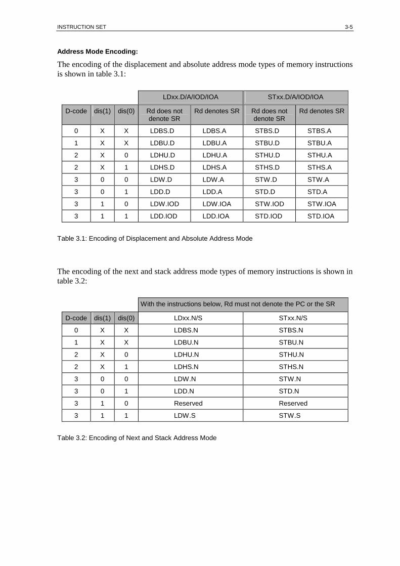
INSTRUCTION SET 3-5
Address Mode Encoding:
The encoding of the displacement and absolute address mode types of memory instructions is shown in table 3.1:
LDxx.D/A/IOD/IOA STxx.D/A/IOD/IOA
D-code dis(1) dis(0) Rd does not denote SR
Rd denotes SR Rd does not denote SR
Rd denotes SR
0 X X LDBS.D LDBS.A STBS.D STBS.A
1 X X LDBU.D LDBU.A STBU.D STBU.A
2 X 0 LDHU.D LDHU.A STHU.D STHU.A
2 X 1 LDHS.D LDHS.A STHS.D STHS.A
3 0 0 LDW.D LDW.A STW.D STW.A
3 0 1 LDD.D LDD.A STD.D STD.A
3 1 0 LDW.IOD LDW.IOA STW.IOD STW.IOA
3 1 1 LDD.IOD LDD.IOA STD.IOD STD.IOA
Table 3.1: Encoding of Displacement and Absolute Address Mode
The encoding of the next and stack address mode types of memory instructions is shown in table 3.2:
With the instructions below, Rd must not denote the PC or the SR
D-code dis(1) dis(0) LDxx.N/S STxx.N/S
0 X X LDBS.N STBS.N
1 X X LDBU.N STBU.N
2 X 0 LDHU.N STHU.N
2 X 1 LDHS.N STHS.N
3 0 0 LDW.N STW.N
3 0 1 LDD.N STD.N
3 1 0 Reserved Reserved
3 1 1 LDW.S STW.S
Table 3.2: Encoding of Next and Stack Address Mode

3-6 CHAPTER 3
3.1.2. Load Instructions The Load instructions transfer data from the addressed memory location into a register Rs or a register pair Rs//Rsf.
In the case of data types word and double-word, one or two words are read from memory and transferred unchanged into Rs or Rs//Rsf respectively.
In the case of byte and half-word data types, up to one word (depending on bus size) is read from memory, the byte or half-word addressed by bits one and zero or bit one of the mem-ory address respectively is extracted, right adjusted, expanded to 32 bits and placed in Rs. Unsigned bytes and half-words are expanded by leading zeros; signed bytes and half-words are expanded by leading sign bits.
Execution of a Load instruction enters the register address of Rs, memory address bits one and zero and a code for the data type into the load pipeline, places the memory address onto the address bus and starts a memory cycle. A double-word Load instruction enters the register address of Rsf and the same control information into the load pipeline as a second entry, places the memory address incremented by four onto the address bus and starts a second memory cycle.
After execution of a Load instruction, the next instructions are executed without waiting for the data to be loaded. A wait is enforced only if an instruction uses a register whose register address is still in the load pipeline. The data read from memory is placed in the register whose register address is at the head of the load pipeline, its pipeline entry is then deleted.
Rs must not denote the PC, the SR, G14 or G15; these registers cannot be loaded from memory.

INSTRUCTION SET 3-7
3.1.2. Load Instructions (continued)
Format Notation Operation Data Type xx
LR LDxx.R Ld, Rs Rs := Ld^; W,D [Rsf := (Ld + 4)^;] -- register address mode
LR LDxx.P Ld, Rs Rs := Ld^; Ld := Ld + size; -- size = 4 or 8 W,D [Rsf := (old Ld + 4)^;] -- post-increment address mode
RRdis LDxx.D Rd, Rs, dis Rs := (Rd + dis)^; BU,BS,HU,HS,W,D [Rsf := (Rd + dis + 4)^;] -- displacement address mode
RRdis LDxx.A 0, Rs, dis Rs := dis^; BU,BS,HU,HS,W,D [Rsf := (dis + 4)^;] -- absolute address mode
RRdis LDxx.IOD Rd, Rs, dis Rs := (Rd + dis)^; W,D [Rsf := (Rd + dis + 4)^;] -- I/O displacement address mode
RRdis LDxx.IOA 0, Rs, dis Rs := dis^; W,D [Rsf := (dis + 4)^;] -- I/O absolute address mode
RRdis LDxx.N Rd, Rs, dis Rs := Rd^; Rd := Rd + dis; BU,BS,HU,HS,W,D [Rsf := (old Rd + 4)^;] -- next address mode
RRdis LDxx.S Rd, Rs, dis Rs := Rd^; Rd := Rd + dis; W -- stack address mode
The expressions in brackets are only executed at double-word data types.
Data Type xx is with:
BU: byte unsigned; HU: half-word unsigned; W: word; BS: byte signed; HS: half-word signed; D: double-word;
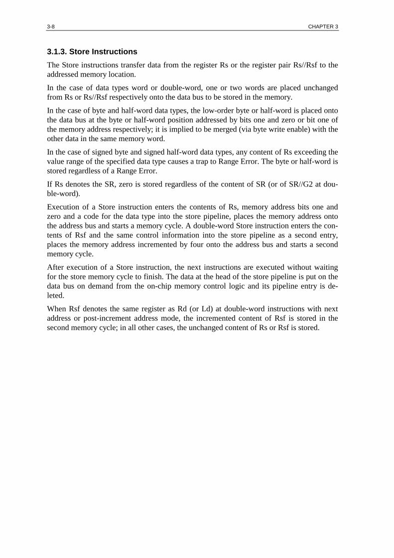
3-8 CHAPTER 3
3.1.3. Store Instructions The Store instructions transfer data from the register Rs or the register pair Rs//Rsf to the addressed memory location.
In the case of data types word or double-word, one or two words are placed unchanged from Rs or Rs//Rsf respectively onto the data bus to be stored in the memory.
In the case of byte and half-word data types, the low-order byte or half-word is placed onto the data bus at the byte or half-word position addressed by bits one and zero or bit one of the memory address respectively; it is implied to be merged (via byte write enable) with the other data in the same memory word.
In the case of signed byte and signed half-word data types, any content of Rs exceeding the value range of the specified data type causes a trap to Range Error. The byte or half-word is stored regardless of a Range Error.
If Rs denotes the SR, zero is stored regardless of the content of SR (or of SR//G2 at dou-ble-word).
Execution of a Store instruction enters the contents of Rs, memory address bits one and zero and a code for the data type into the store pipeline, places the memory address onto the address bus and starts a memory cycle. A double-word Store instruction enters the con-tents of Rsf and the same control information into the store pipeline as a second entry, places the memory address incremented by four onto the address bus and starts a second memory cycle.
After execution of a Store instruction, the next instructions are executed without waiting for the store memory cycle to finish. The data at the head of the store pipeline is put on the data bus on demand from the on-chip memory control logic and its pipeline entry is de-leted.
When Rsf denotes the same register as Rd (or Ld) at double-word instructions with next address or post-increment address mode, the incremented content of Rsf is stored in the second memory cycle; in all other cases, the unchanged content of Rs or Rsf is stored.

INSTRUCTION SET 3-9
3.1.3. Store Instructions (continued)
Format Notation Operation Data Type xx
LR STxx.R Ld, Rs Ld^ := Rs; W,D [(Ld + 4)^ := Rsf;] -- register address mode
LR STxx.P Ld, Rs Ld^ := Rs; Ld := Ld + size; -- size = 4 or 8 W,D [(old Ld + 4)^ := Rsf;] -- post-increment address mode
RRdis STxx.D Rd, Rs, dis (Rd + dis)^ := Rs; BU,BS,HU,HS,W,D [(Rd + dis + 4)^ := Rsf;] -- displacement address mode
RRdis STxx.A 0, Rs, dis dis^ := Rs; BU,BS,HU,HS,W,D [(dis + 4)^ := Rsf;] -- absolute address mode
RRdis STxx.IOD Rd, Rs, dis (Rd + dis)^ := Rs; W,D [(Rd + dis + 4)^ := Rsf;] -- I/O displacement address mode
RRdis STxx.IOA 0, Rs, dis dis^ := Rs; W,D [(dis + 4)^ := Rsf;] -- I/O absolute address mode
RRdis STxx.N Rd, Rs, dis Rd^ := Rs; Rd := Rd + dis; BU,BS,HU,HS,W,D [(old Rd + 4)^ := Rsf;] -- next address mode
RRdis STxx.S Rd, Rs, dis Rd^ := Rs; Rd := Rd + dis; W -- stack address mode
The expressions in brackets are only executed at double-word data types.
In the case of signed byte and half-word data types, a trap to Range Error occurs when the value of the operand to be stored exceeds the value range of the specified data type; the byte or half-word is stored regardless of a Range Error.
Data Type xx is with:
BU: byte unsigned; HU: half-word unsigned; W: word; BS: byte signed; HS: half-word signed; D: double-word;

3-10 CHAPTER 3
3.2. Move Word Instructions The source operand or the immediate operand is copied to the destination register and the condition flags are set or cleared accordingly.
Format Notation Operation
RR MOV Rd, Rs Rd := Rs; Z := Rd = 0; N := Rd(31); V := undefined;
Rimm MOVI Rd, imm Rd := imm; Z := Rd = 0; N := Rd(31); V := undefined;
3.3. Move Double-Word Instruction The double-word source operand is copied to the double-word destination register pair and the condition flags are set or cleared accordingly. The high-order word in Rs is copied first.
When the SR is denoted as a source operand, the source operand is supplied as zero regard-less of the content of SR//G2. When the PC is denoted as destination, the Return instruc-tion RET is executed instead of the Move Double-Word instruction.
Format Notation Operation
RR MOVD Rd, Rs if Rd does not denote PC and Rs does not denote SR then Rd := Rs; Rdf := Rsf; Z := Rd//Rdf = 0; N := Rd(31); V := undefined;
RR MOVD Rd, 0 if Rd does not denote PC and Rs denotes SR then Rd := 0; Rdf := 0; Z := 1; N := 0; V := undefined;
RR RET PC, Rs if Rd denotes PC then execute the RET instruction;
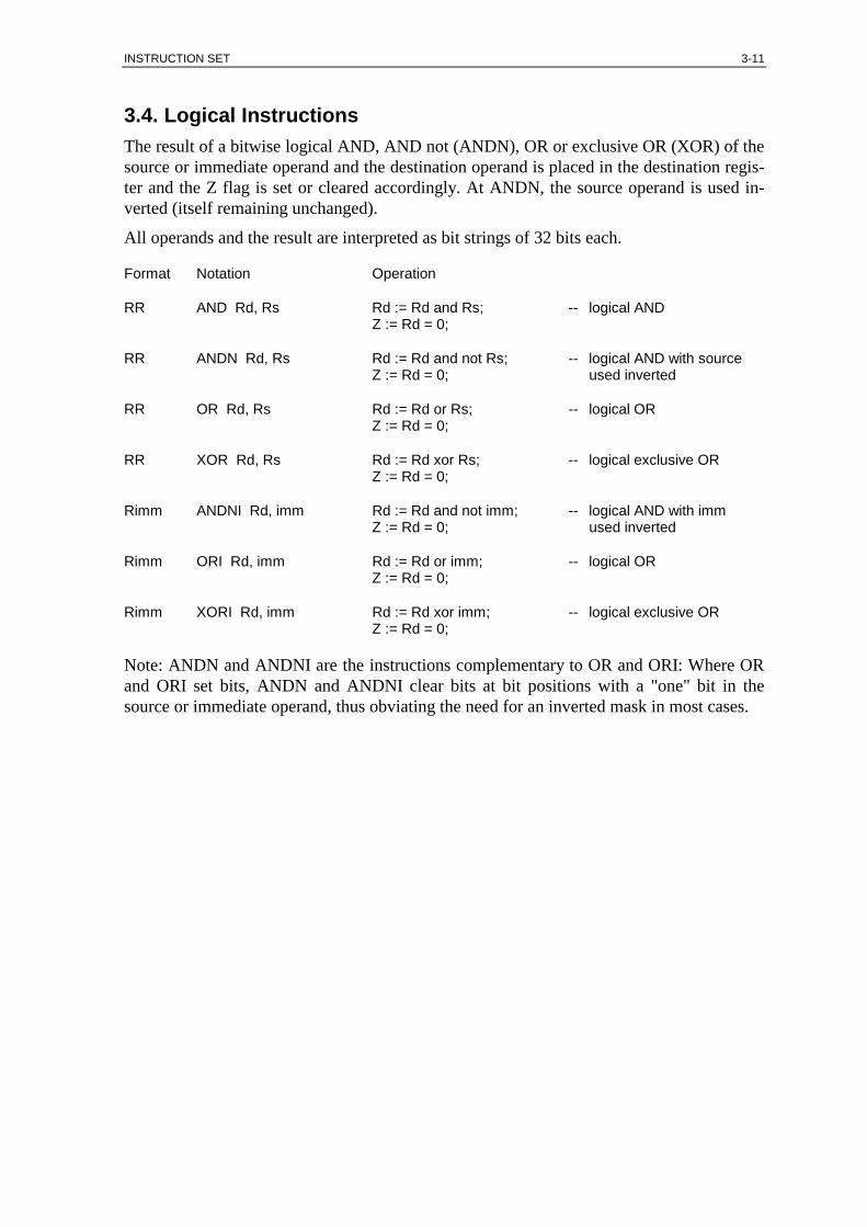
INSTRUCTION SET 3-11
3.4. Logical Instructions The result of a bitwise logical AND, AND not (ANDN), OR or exclusive OR (XOR) of the source or immediate operand and the destination operand is placed in the destination regis-ter and the Z flag is set or cleared accordingly. At ANDN, the source operand is used in-verted (itself remaining unchanged).
All operands and the result are interpreted as bit strings of 32 bits each.
Format Notation Operation
RR AND Rd, Rs Rd := Rd and Rs; -- logical AND Z := Rd = 0;
RR ANDN Rd, Rs Rd := Rd and not Rs; -- logical AND with source Z := Rd = 0; used inverted
RR OR Rd, Rs Rd := Rd or Rs; -- logical OR Z := Rd = 0;
RR XOR Rd, Rs Rd := Rd xor Rs; -- logical exclusive OR Z := Rd = 0;
Rimm ANDNI Rd, imm Rd := Rd and not imm; -- logical AND with imm Z := Rd = 0; used inverted
Rimm ORI Rd, imm Rd := Rd or imm; -- logical OR Z := Rd = 0;
Rimm XORI Rd, imm Rd := Rd xor imm; -- logical exclusive OR Z := Rd = 0;
Note: ANDN and ANDNI are the instructions complementary to OR and ORI: Where OR and ORI set bits, ANDN and ANDNI clear bits at bit positions with a "one" bit in the source or immediate operand, thus obviating the need for an inverted mask in most cases.

3-12 CHAPTER 3
3.5. Invert Instruction The source operand is placed bitwise inverted in the destination register and the Z flag is set or cleared accordingly.
The source operand and the result are interpreted as bit strings of 32 bits each.
Format Notation Operation
RR NOT Rd, Rs Rd := not Rs; Z := Rd = 0;
3.6. Mask Instruction The result of a bitwise logical AND of the source operand and the immediate operand is placed in the destination register and the Z flag is set or cleared accordingly.
All operands and the result are interpreted as bit strings of 32 bits each.
Format Notation Operation
RRconst MASK Rd, Rs, const Rd := Rs and const; Z := Rd = 0;
Note: The Mask instruction may be used to move a source operand with bits partly masked out by an immediate operand used as mask. The immediate operand const is constrained in its range by bits 31 and 30 being either both zero or both one (see format RRconst). If these bits are required to be different, the instruction pair MOVI, AND may be used instead of MASK.

INSTRUCTION SET 3-13
3.7. Add Instructions The source operand, the source operand + C or the immediate operand is added to the des-tination operand, the result is placed in the destination register and the condition flags are set or cleared accordingly.
At ADD, ADDC and ADDI, both operands and the result are interpreted as either all signed or all unsigned integers. At ADDS and ADDSI, both operands and the result are signed integers and a trap to Range Error occurs at overflow.
Format Notation Operation
RR ADD Rd, Rs Rd := Rd + Rs; -- signed or unsigned Add Z := Rd = 0; N := Rd(31); -- sign V := overflow; C := carry;
RR ADDS Rd, Rs Rd := Rd + Rs; -- signed Add with trap Z := Rd = 0; N := Rd(31); -- sign V := overflow; if overflow then trap ⇒ Range Error;
RR ADDC Rd, Rs Rd := Rd + Rs + C; -- signed or unsigned Add Z := Z and (Rd = 0); with carry N := Rd(31); -- sign V := overflow; C := carry;
When the SR is denoted as a source operand at ADD, ADDS and ADDC, C is added in-stead of the SR. The notation is then:
Format Notation Operation
RR ADD Rd, C Rd := Rd + C; -- signed or unsigned Add C
RR ADDS Rd, C Rd := Rd + C; -- signed Add C with trap
RR ADDC Rd, C Rd := Rd + C;
The flags and the trap condition are treated as defined by ADD, ADDS or ADDC.

3-14 CHAPTER 3
3.7. Add Instructions (continued) Format Notation Operation
Rimm ADDI Rd, imm Rd := Rd + imm; -- signed or unsigned Add Z := Rd = 0; N := Rd(31); -- sign V := overflow; C := carry;
Rimm ADDSI Rd, imm Rd := Rd + imm; -- signed Add with trap Z := Rd = 0; N := Rd(31); -- sign V := overflow; if overflow then trap ⇒ Range Error;
The following instructions are special cases of ADDI and ADDSI differentiated by n = 0 (see section 2.3.1. Table of Immediate Values):
Format Notation Operation
Rimm ADDI Rd, CZ Rd := Rd + (C and (Z = 0 or Rd(0))); -- round to even
Rimm ADDSI Rd, CZ Rd := Rd + (C and (Z = 0 or Rd(0))); -- round to even
The flags and the trap condition are treated as defined by ADDI or ADDSI.
Note: At ADDC, Z is cleared if Rd ≠ 0, otherwise left unchanged; thus, Z is evaluated cor-rectly for multi-precision operands.
The effect of a Subtract immediate instruction can be obtained by using the negated 32-bit value of the immediate operand to be subtracted (except zero). At unsigned, C = 0 indicates then a borrow (the unsigned number range is exceeded below zero).
At "round to even", C is only added to the destination operand if Z = 0 or Rd(0) is one. The Z flag is assumed to be set or cleared by a preceding Shift Left instruction. "Round to even" provides a better averaging of rounding errors than "add carry".
"Round to even" is equivalent to the "round to nearest" Floating-Point rounding mode and may be used to implement it efficiently.
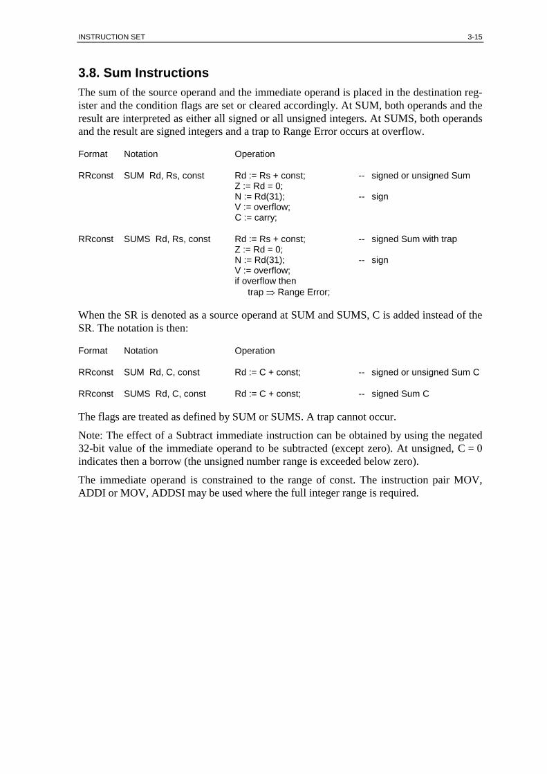
INSTRUCTION SET 3-15
3.8. Sum Instructions The sum of the source operand and the immediate operand is placed in the destination reg-ister and the condition flags are set or cleared accordingly. At SUM, both operands and the result are interpreted as either all signed or all unsigned integers. At SUMS, both operands and the result are signed integers and a trap to Range Error occurs at overflow.
Format Notation Operation
RRconst SUM Rd, Rs, const Rd := Rs + const; -- signed or unsigned Sum Z := Rd = 0; N := Rd(31); -- sign V := overflow; C := carry;
RRconst SUMS Rd, Rs, const Rd := Rs + const; -- signed Sum with trap Z := Rd = 0; N := Rd(31); -- sign V := overflow; if overflow then trap ⇒ Range Error;
When the SR is denoted as a source operand at SUM and SUMS, C is added instead of the SR. The notation is then:
Format Notation Operation
RRconst SUM Rd, C, const Rd := C + const; -- signed or unsigned Sum C
RRconst SUMS Rd, C, const Rd := C + const; -- signed Sum C
The flags are treated as defined by SUM or SUMS. A trap cannot occur.
Note: The effect of a Subtract immediate instruction can be obtained by using the negated 32-bit value of the immediate operand to be subtracted (except zero). At unsigned, C = 0 indicates then a borrow (the unsigned number range is exceeded below zero).
The immediate operand is constrained to the range of const. The instruction pair MOV, ADDI or MOV, ADDSI may be used where the full integer range is required.

3-16 CHAPTER 3
3.9. Subtract Instructions The source operand or the source operand + C is subtracted from the destination operand, the result is placed in the destination register and the condition flags are set or cleared ac-cordingly.
At SUB and SUBC, both operands and the result are interpreted as either all signed or all unsigned integers. At SUBS, both operands and the result are signed integers and a trap to Range Error occurs at overflow.
Format Notation Operation
RR SUB Rd, Rs Rd := Rd - Rs; -- signed or unsigned Subtract Z := Rd = 0; N := Rd(31); -- sign V := overflow; C := borrow;
RR SUBS Rd, Rs Rd := Rd - Rs; -- signed Subtract with trap Z := Rd = 0; N := Rd(31); -- sign V := overflow; if overflow then trap ⇒ Range Error;
RR SUBC Rd, Rs Rd := Rd - (Rs + C); -- signed or unsigned Subtract Z := Z and (Rd = 0); with borrow N := Rd(31); -- sign V := overflow; C := borrow;
When the SR is denoted as a source operand at SUB, SUBS and SUBC, C is subtracted instead of the SR. The notation is then:
Format Notation Operation
RR SUB Rd, C Rd := Rd - C; -- signed or unsigned Subtract C
RR SUBS Rd, C Rd := Rd - C; -- signed Subtract C with trap
RR SUBC Rd, C Rd := Rd - C;
The flags and the trap condition are treated as defined by SUB, SUBS or SUBC.
Note: At SUBC, Z is cleared if Rd ≠ 0, otherwise left unchanged; thus, Z is evaluated cor-rectly for multi-precision operands.

INSTRUCTION SET 3-17
3.10. Negate Instructions The source operand is subtracted from zero, the result is placed in the destination register and the condition flags are set or cleared accordingly.
At NEG and NEGS, the source operand and the result are interpreted as either both signed or both unsigned integers. At NEGS, the source operand and the result are signed integers and a trap to Range Error occurs at overflow.
Format Notation Operation
RR NEG Rd, Rs Rd := - Rs; -- signed or unsigned Negate Z := Rd = 0; N := Rd(31); -- sign V := overflow; C := borrow;
RR NEGS Rd, Rs Rd := - Rs; -- signed Negate with trap Z := Rd = 0; N := Rd(31); -- sign V := overflow; if overflow then trap ⇒ Range Error;
When the SR is denoted as a source operand at NEG and NEGS, C is negated instead of the SR. The notation is then:
Format Notation Operation
RR NEG Rd, C Rd := - C; -- signed or unsigned Negate C if C is set then Rd := -1; else Rd := 0;
RR NEGS Rd, C Rd := - C; -- signed Negate C if C is set then Rd := -1; else Rd := 0;
The flags are treated as defined by NEG or NEGS. A trap cannot occur.

3-18 CHAPTER 3
3.11. Multiply Word Instruction The source operand and the destination operand are multiplied, the low-order word of the product is placed in the destination register (the high-order product word is not evaluated) and the condition flags are set or cleared according to the single-word product.
Both operands are either signed or unsigned integers, the product is a single-word integer.
Note that the low-order word of the product is identical regardless of whether the operands are signed or unsigned.
The result is undefined if the PC or the SR is denoted.
Format Notation Operation
RR MUL Rd, Rs Rd := low order word of product Rd ∗ Rs; Z := single-word product = 0; N := Rd(31); -- sign of single-word product; -- valid for signed operands; V := undefined; C := undefined;
3.12. Multiply Double-Word Instructions The source operand and the destination operand are multiplied, the double-word product is placed in the destination register pair (the destination register expanded by the register fol-lowing it) and the condition flags are set or cleared according to the double-word product.
At MULS, both operands are signed integers and the product is a signed double-word inte-ger. At MULU, both operands are unsigned integers and the product is an unsigned double-word integer.
The result is undefined if the PC or the SR is denoted.
Format Notation Operation
RR MULS Rd, Rs Rd//Rdf := signed double-word product of Rd ∗ Rs; Z := Rd//Rdf = 0; -- double-word product is zero N := Rd(31); -- double-word product is negative V := undefined; C := undefined;
RR MULU Rd, Rs Rd//Rdf := unsigned double-word product of Rd ∗ Rs; Z := Rd//Rdf = 0; -- double-word product is zero N := Rd(31); V := undefined; C := undefined;
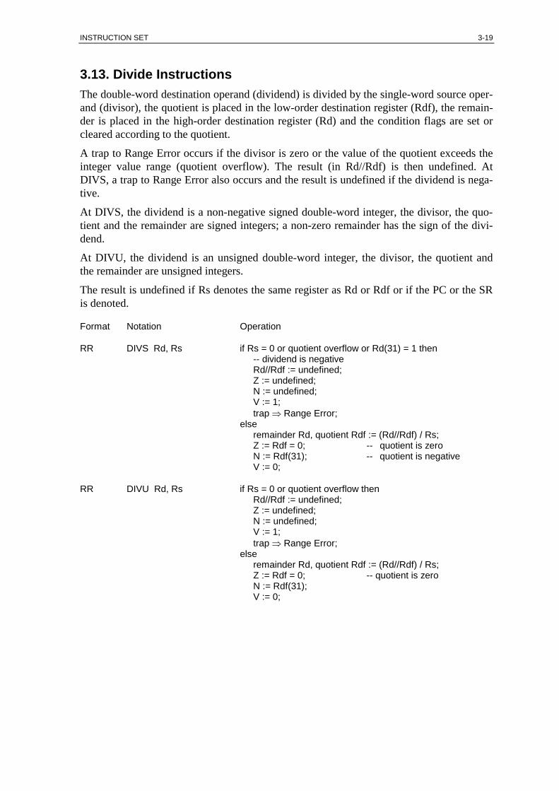
INSTRUCTION SET 3-19
3.13. Divide Instructions The double-word destination operand (dividend) is divided by the single-word source oper-and (divisor), the quotient is placed in the low-order destination register (Rdf), the remain-der is placed in the high-order destination register (Rd) and the condition flags are set or cleared according to the quotient.
A trap to Range Error occurs if the divisor is zero or the value of the quotient exceeds the integer value range (quotient overflow). The result (in Rd//Rdf) is then undefined. At DIVS, a trap to Range Error also occurs and the result is undefined if the dividend is nega-tive.
At DIVS, the dividend is a non-negative signed double-word integer, the divisor, the quo-tient and the remainder are signed integers; a non-zero remainder has the sign of the divi-dend.
At DIVU, the dividend is an unsigned double-word integer, the divisor, the quotient and the remainder are unsigned integers.
The result is undefined if Rs denotes the same register as Rd or Rdf or if the PC or the SR is denoted.
Format Notation Operation
RR DIVS Rd, Rs if Rs = 0 or quotient overflow or Rd(31) = 1 then -- dividend is negative Rd//Rdf := undefined; Z := undefined; N := undefined; V := 1; trap ⇒ Range Error; else remainder Rd, quotient Rdf := (Rd//Rdf) / Rs; Z := Rdf = 0; -- quotient is zero N := Rdf(31); -- quotient is negative V := 0;
RR DIVU Rd, Rs if Rs = 0 or quotient overflow then Rd//Rdf := undefined; Z := undefined; N := undefined; V := 1; trap ⇒ Range Error; else remainder Rd, quotient Rdf := (Rd//Rdf) / Rs; Z := Rdf = 0; -- quotient is zero N := Rdf(31); V := 0;
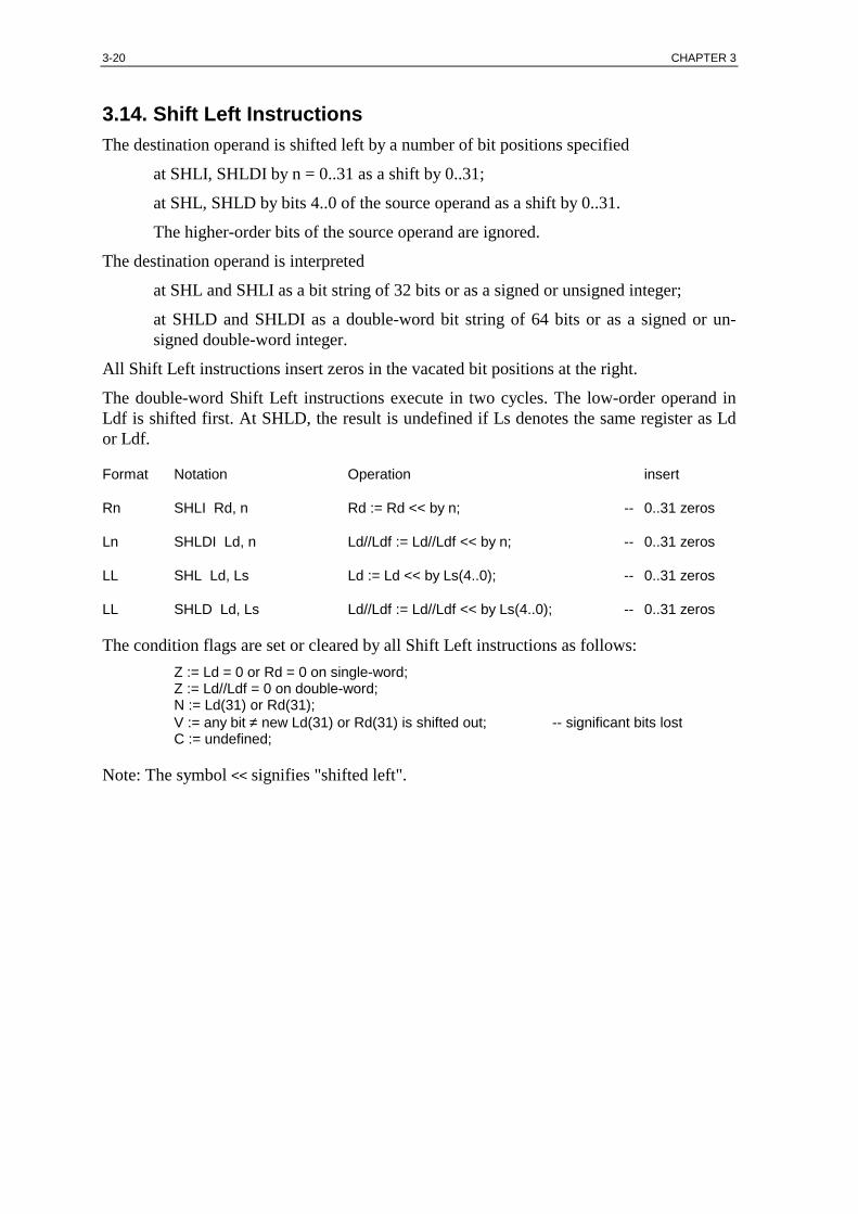
3-20 CHAPTER 3
3.14. Shift Left Instructions The destination operand is shifted left by a number of bit positions specified
at SHLI, SHLDI by n = 0..31 as a shift by 0..31;
at SHL, SHLD by bits 4..0 of the source operand as a shift by 0..31.
The higher-order bits of the source operand are ignored.
The destination operand is interpreted
at SHL and SHLI as a bit string of 32 bits or as a signed or unsigned integer;
at SHLD and SHLDI as a double-word bit string of 64 bits or as a signed or un-signed double-word integer.
All Shift Left instructions insert zeros in the vacated bit positions at the right.
The double-word Shift Left instructions execute in two cycles. The low-order operand in Ldf is shifted first. At SHLD, the result is undefined if Ls denotes the same register as Ld or Ldf.
Format Notation Operation insert
Rn SHLI Rd, n Rd := Rd << by n; -- 0..31 zeros
Ln SHLDI Ld, n Ld//Ldf := Ld//Ldf << by n; -- 0..31 zeros
LL SHL Ld, Ls Ld := Ld << by Ls(4..0); -- 0..31 zeros
LL SHLD Ld, Ls Ld//Ldf := Ld//Ldf << by Ls(4..0); -- 0..31 zeros
The condition flags are set or cleared by all Shift Left instructions as follows: Z := Ld = 0 or Rd = 0 on single-word; Z := Ld//Ldf = 0 on double-word; N := Ld(31) or Rd(31); V := any bit ≠ new Ld(31) or Rd(31) is shifted out; -- significant bits lost C := undefined;
Note: The symbol << signifies "shifted left".

INSTRUCTION SET 3-21
3.15. Shift Right Instructions The destination operand is shifted right by a number of bit positions specified
at SARI, SARDI, SHRI, SHRDI by n = 0..31 as a shift by 0..31.
at SAR, SARD, SHR, SHRD by bits 4..0 of the source operand as a shift by 0..31.
The higher-order bits of the source operand are ignored.
The destination operand is interpreted
at SAR and SARI as a signed integer;
at SARD and SARDI as a signed double-word integer;
at SHR and SHRI as a bit string of 32 bits or as an unsigned integer;
at SHRD and SHRDI as a double-word bit string of 64 bits or as an unsigned dou-ble-word integer.
All Shift Right instructions which interpret the destination operand as signed insert sign bits, all others insert zeros in the vacated bit positions at the left.
The double-word Shift Right instructions execute in two cycles. The high-order operand in Ld is shifted first. At SARD and SHRD, the result is undefined if Ls denotes the same reg-ister as Ld or Ldf.
Format Notation Operation insert
Rn SARI Rd, n Rd := Rd >> by n; -- 0..31 sign bits
Ln SARDI Ld, n Ld//Ldf := Ld//Ldf >> by n; -- 0..31 sign bits
LL SAR Ld, Ls Ld := Ld >> by Ls(4..0); -- 0..31 sign bits
LL SARD Ld, Ls Ld//Ldf := Ld//Ldf >> by Ls(4..0); -- 0..31 sign bits
Rn SHRI Rd, n Rd := Rd >> by n; -- 0..31 zeros
Ln SHRDI Ld, n Ld//Ldf := Ld//Ldf >> by n; -- 0..31 zeros
LL SHR Ld, Ls Ld := Ld >> by Ls(4..0); -- 0..31 zeros
LL SHRD Ld, Ls Ld//Ldf := Ld//Ldf >> by Ls(4..0); -- 0..31 zeros
The condition flags are set or cleared by all Shift Right instructions as follows: Z := Ld = 0 or Rd = 0 on single-word; Z := Ld//Ldf = 0 on double-word; N := Ld(31) or Rd(31); C := last bit shifted out is "one";
Note: The symbol >> signifies "shifted right".

3-22 CHAPTER 3
3.16. Rotate Left Instruction The destination operand is shifted left by a number of bit positions and the bits shifted out are inserted in the vacated bit positions; thus, the destination operand is rotated. The condi-tion flags are set or cleared accordingly. Bits 4..0 of the source operand specify a rotation by 0..31 bit positions; bits 31..5 of the source operand are ignored.
The destination operand is interpreted as a bit string of 32 bits.
Format Notation Operation
LL ROL Ld, Ls Ld := Ld rotated left by Ls(4..0); Z := Ld = 0; N := Ld(31); V := undefined; C := undefined;

INSTRUCTION SET 3-23
3.17. Index Move Instructions The source operand is placed shifted left by 0, 1, 2 or 3 bit positions in the destination reg-ister, corresponding to a multiplication by 1, 2, 4 or 8. At XM1..XM8, a trap to Range Er-ror occurs if the source operand is higher than the immediate operand lim (upper bound).
All condition flags remain unchanged. All operands and the result are interpreted as un-signed integers.
The SR must not be denoted as a source nor as a destination, nor the PC as a destination operand; these notations are reserved for future expansion. When the PC is denoted as a source operand, a trap to Range Error occurs if PC ≥ lim.
X-code Format Notation Operation
0 RRlim XM1 Rd, Rs, lim Rd := Rs ∗ 1; if Rs > lim then trap ⇒ Range Error;
1 RRlim XM2 Rd, Rs, lim Rd := Rs ∗ 2; if Rs > lim then trap ⇒ Range Error;
2 RRlim XM4 Rd, Rs, lim Rd := Rs ∗ 4; if Rs > lim then trap ⇒ Range Error;
3 RRlim XM8 Rd, Rs, lim Rd := Rs ∗ 8; if Rs > lim then trap ⇒ Range Error;
4 RRlim XX1 Rd, Rs, 0 Rd := Rs ∗ 1; -- Move without flag change
5 RRlim XX2 Rd, Rs, 0 Rd := Rs ∗ 2;
6 RRlim XX4 Rd, Rs, 0 Rd := Rs ∗ 4;
7 RRlim XX8 Rd, Rs, 0 Rd := Rs ∗ 8;
Note: The Index Move instructions move an index value scaled (multiplied by 1, 2, 4 or 8). XM1..XM8 check also the unscaled value for an upper bound, optionally also excluding zero. If the lower bound is not zero, it may be mapped to zero by subtracting it from the index value before applying an Index Move instruction.

3-24 CHAPTER 3
3.18. Check Instructions The destination operand is checked and a trap to Range Error occurs
at CHK if the destination operand is higher than the source operand,
at CHKZ if the destination operand is zero.
All registers and all condition flags remain unchanged. All operands are interpreted as un-signed integers.
CHKZ shares its basic OP-code with CHK, it is differentiated by denoting the SR as source operand.
Format Notation Operation
RR CHK Rd, Rs if Rs does not denote SR and Rd > Rs then trap ⇒ Range Error;
RR CHKZ Rd, 0 if Rs denotes SR and Rd = 0 then trap ⇒ Range Error;
When Rs denotes the PC, CHK traps if Rd ≥ PC. Thus, CHK, PC, PC always traps. Since CHK, PC, PC is encoded as 16 zeros, an erroneous jump into a string of zeros causes a trap to Range Error, thus trapping some address errors.
Note: CHK checks the upper bound of an unsigned value range, implying a lower bound of zero. If the lower bound is not zero, it can be mapped to zero by subtracting it from the value to be checked and then checking against a corrected upper bound (lower bound also subtracted). When the upper bound is a constant not exceeding the range of lim, the Index instructions may be used for bounds checks.
CHKZ may be used to trap on uninitialized pointers with the value zero.
3.19. No Operation Instruction The instruction CHK, L0, L0 cannot cause any trap. Since CHK leaves all registers and condition flags unchanged, it can be used as a No Operation instruction with the notation:
Format Notation Operation
RR NOP no operation;
Note: The NOP instruction may be used as a fill instruction.

INSTRUCTION SET 3-25
3.20. Compare Instructions Two operands are compared by subtracting the source operand or the immediate operand from the destination operand. The condition flags are set or cleared according to the result; the result itself is not retained. Note that the N flag indicates the correct compare result even in the case of an overflow.
All operands and the result are interpreted as either all signed or all unsigned integers.
Format Notation Operation
RR CMP Rd, Rs result := Rd - Rs; Z := Rd = Rs; -- result is zero N := Rd < Rs signed; -- result is true negative V := overflow; C := Rd < Rs unsigned; -- borrow
Rimm CMPI Rd, imm result := Rd - imm; Z := Rd = imm; -- result is zero N := Rd < imm signed; -- result is true negative V := overflow; C := Rd < imm unsigned; -- borrow
When the SR is denoted as a source operand at CMP, C is subtracted instead of SR. The notation is then:
Format Notation Operation
RR CMP, Rd, C result := Rd - C; Z := Rd = C; -- result is zero N := Rd < C signed; -- result is true negative V := overflow; C := Rd < C unsigned; -- borrow
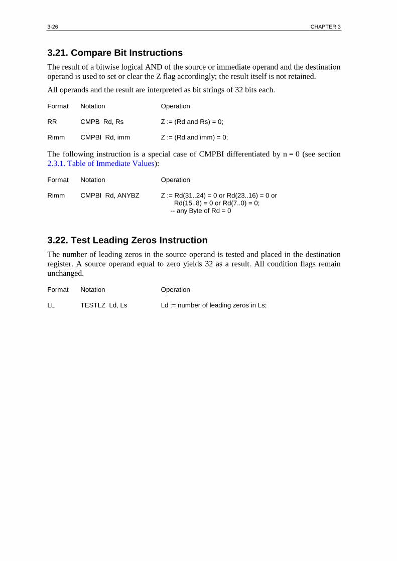
3-26 CHAPTER 3
3.21. Compare Bit Instructions The result of a bitwise logical AND of the source or immediate operand and the destination operand is used to set or clear the Z flag accordingly; the result itself is not retained.
All operands and the result are interpreted as bit strings of 32 bits each.
Format Notation Operation
RR CMPB Rd, Rs Z := (Rd and Rs) = 0;
Rimm CMPBI Rd, imm Z := (Rd and imm) = 0;
The following instruction is a special case of CMPBI differentiated by n = 0 (see section 2.3.1. Table of Immediate Values):
Format Notation Operation
Rimm CMPBI Rd, ANYBZ Z := Rd(31..24) = 0 or Rd(23..16) = 0 or Rd(15..8) = 0 or Rd(7..0) = 0; -- any Byte of Rd = 0
3.22. Test Leading Zeros Instruction The number of leading zeros in the source operand is tested and placed in the destination register. A source operand equal to zero yields 32 as a result. All condition flags remain unchanged.
Format Notation Operation
LL TESTLZ Ld, Ls Ld := number of leading zeros in Ls;
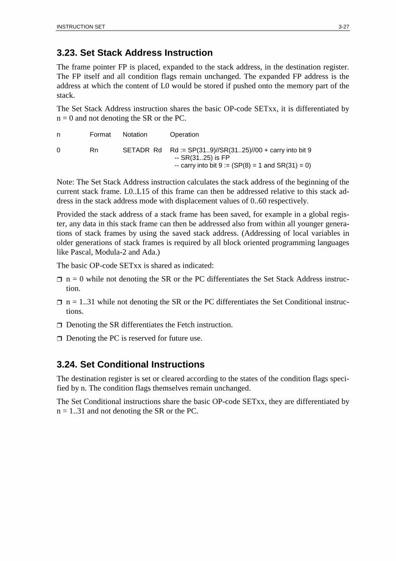
INSTRUCTION SET 3-27
3.23. Set Stack Address Instruction The frame pointer FP is placed, expanded to the stack address, in the destination register. The FP itself and all condition flags remain unchanged. The expanded FP address is the address at which the content of L0 would be stored if pushed onto the memory part of the stack.
The Set Stack Address instruction shares the basic OP-code SETxx, it is differentiated by n = 0 and not denoting the SR or the PC.
n Format Notation Operation
0 Rn SETADR Rd Rd := SP(31..9)//SR(31..25)//00 + carry into bit 9 -- SR(31..25) is FP -- carry into bit 9 := (SP(8) = 1 and SR(31) = 0)
Note: The Set Stack Address instruction calculates the stack address of the beginning of the current stack frame. L0..L15 of this frame can then be addressed relative to this stack ad-dress in the stack address mode with displacement values of 0..60 respectively.
Provided the stack address of a stack frame has been saved, for example in a global regis-ter, any data in this stack frame can then be addressed also from within all younger genera-tions of stack frames by using the saved stack address. (Addressing of local variables in older generations of stack frames is required by all block oriented programming languages like Pascal, Modula-2 and Ada.)
The basic OP-code SETxx is shared as indicated:
n = 0 while not denoting the SR or the PC differentiates the Set Stack Address instruc-tion.
n = 1..31 while not denoting the SR or the PC differentiates the Set Conditional instruc-tions.
Denoting the SR differentiates the Fetch instruction.
Denoting the PC is reserved for future use.
3.24. Set Conditional Instructions The destination register is set or cleared according to the states of the condition flags speci-fied by n. The condition flags themselves remain unchanged.
The Set Conditional instructions share the basic OP-code SETxx, they are differentiated by n = 1..31 and not denoting the SR or the PC.

3-28 CHAPTER 3
3.24. Set Conditional Instructions (continued) Format is Rn
n Notation or Alternative Operation
1 Reserved
2 SET1 Rd Rd := 1;
3 SET0 Rd Rd := 0;
4 SETLE Rd if N = 1 or Z = 1 then Rd := 1 else Rd := 0;
5 SETGT Rd if N = 0 and Z = 0 then Rd := 1 else Rd := 0;
6 SETLT Rd SETN Rd if N = 1 then Rd := 1 else Rd := 0;
7 SETGE Rd SETNN Rd if N = 0 then Rd := 1 else Rd := 0;
8 SETSE Rd if C = 1 or Z = 1 then Rd := 1 else Rd := 0;
9 SETHT Rd if C = 0 and Z = 0 then Rd := 1 else Rd := 0;
10 SETST Rd SETC Rd if C = 1 then Rd := 1 else Rd := 0;
11 SETHE Rd SETNC Rd if C = 0 then Rd := 1 else Rd := 0;
12 SETE SETZ if Z = 1 then Rd := 1 else Rd := 0;
13 SETNE SETNZ if Z = 0 then Rd := 1 else Rd := 0;
14 SETV Rd if V = 1 then Rd := 1 else Rd := 0;
15 SETNV Rd if V = 0 then Rd := 1 else Rd := 0;
16 Reserved
17 Reserved
18 SET1M Rd Rd := -1;
19 Reserved
20 SETLEM Rd if N = 1 or Z = 1 then Rd := -1 else Rd := 0;
21 SETGTM Rd if N = 0 and Z = 0 then Rd := -1 else Rd := 0;
22 SETLTM Rd SETNM Rd if N = 1 then Rd := -1 else Rd := 0;
23 SETGEM Rd SETNNM Rd if N = 0 then Rd := -1 else Rd := 0;
24 SETSEM Rd if C = 1 or Z = 1 then Rd := -1 else Rd := 0;
25 SETHTM Rd if C = 0 and Z = 0 then Rd := -1 else Rd := 0;
26 SETSTM Rd SETCM Rd if C = 1 then Rd := -1 else Rd := 0;
27 SETHEM Rd SETNCM Rd if C = 0 then Rd := -1 else Rd := 0;
28 SETEM SETZM if Z = 1 then Rd := -1 else Rd := 0;
29 SETNEM SETNZM if Z = 0 then Rd := -1 else Rd := 0;
30 SETVM Rd if V = 1 then Rd := -1 else Rd := 0;
31 SETNVM Rd if V = 0 then Rd := -1 else Rd := 0;
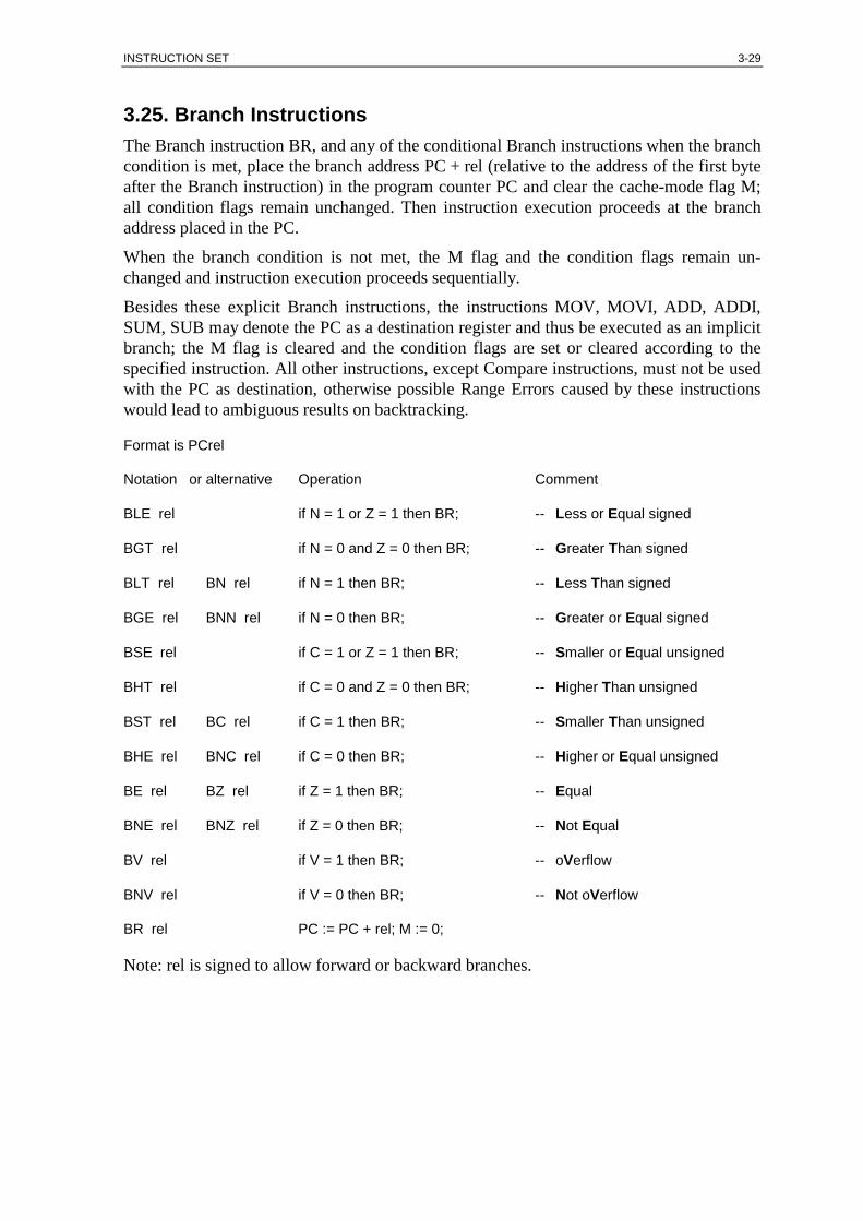
INSTRUCTION SET 3-29
3.25. Branch Instructions The Branch instruction BR, and any of the conditional Branch instructions when the branch condition is met, place the branch address PC + rel (relative to the address of the first byte after the Branch instruction) in the program counter PC and clear the cache-mode flag M; all condition flags remain unchanged. Then instruction execution proceeds at the branch address placed in the PC.
When the branch condition is not met, the M flag and the condition flags remain un-changed and instruction execution proceeds sequentially.
Besides these explicit Branch instructions, the instructions MOV, MOVI, ADD, ADDI, SUM, SUB may denote the PC as a destination register and thus be executed as an implicit branch; the M flag is cleared and the condition flags are set or cleared according to the specified instruction. All other instructions, except Compare instructions, must not be used with the PC as destination, otherwise possible Range Errors caused by these instructions would lead to ambiguous results on backtracking.
Format is PCrel
Notation or alternative Operation Comment
BLE rel if N = 1 or Z = 1 then BR; -- Less or Equal signed
BGT rel if N = 0 and Z = 0 then BR; -- Greater Than signed
BLT rel BN rel if N = 1 then BR; -- Less Than signed
BGE rel BNN rel if N = 0 then BR; -- Greater or Equal signed
BSE rel if C = 1 or Z = 1 then BR; -- Smaller or Equal unsigned
BHT rel if C = 0 and Z = 0 then BR; -- Higher Than unsigned
BST rel BC rel if C = 1 then BR; -- Smaller Than unsigned
BHE rel BNC rel if C = 0 then BR; -- Higher or Equal unsigned
BE rel BZ rel if Z = 1 then BR; -- Equal
BNE rel BNZ rel if Z = 0 then BR; -- Not Equal
BV rel if V = 1 then BR; -- oVerflow
BNV rel if V = 0 then BR; -- Not oVerflow
BR rel PC := PC + rel; M := 0;
Note: rel is signed to allow forward or backward branches.
3-30 CHAPTER 3
3.26. Delayed Branch Instructions The Delayed Branch instruction DBR, and any of the conditional Delayed Branch in-structions when the branch condition is met, place the branch address PC + rel (relative to the address of the first byte after the Delayed Branch instruction) in the program counter PC. All condition flags and the cache mode flag M remain unchanged.
Then the instruction after the Delayed Branch instruction, called the delay instruction, is executed regardless of whether the delayed branch is taken or not taken.
When the delayed branch is not taken, the delay instruction is executed like a regular in-struction. The PC and the ILC are updated accordingly and instruction execution proceeds sequentially.
When the delayed branch is taken, the delay instruction is executed before execution pro-ceeds at the branch target. The PC (containing the delayed-branch target address) is not updated by the delay instruction. Any reference to the PC by the delay instruction refer-ences the delayed-branch target address.
In the case of an Error exception caused by a delay instruction succeeding a delayed branch taken, the location of the saved return PC contains the address of the first byte of the delay instruction. The saved ILC contains the length (1 or 2 half-words) of the Delayed Branch instruction. In the case of all other exceptions following a delay instruction succeeding a delayed branch taken, the location of the saved return PC contains the branch target address of the delayed branch and the saved ILC is invalid.
The following restrictions apply to delay instructions:
The sum of the length of the Delayed Branch instruction and the delay instruction must not exceed three half-words, otherwise an arbitrary bit pattern may be supplied and erroneously used for the second or third half-word of the delay instruction without any warning.
Only a Reset exception can occur between a Delayed Branch instruction and a delay in-struction, all other exceptions are locked out.
A Fetch or any branching instruction must not be placed as a delay instruction. A mis-placed Delayed Branch instruction would be executed like the corresponding non-delayed Branch instruction to inhibit a permanent exception lock-out.

INSTRUCTION SET 3-31
3.26. Delayed Branch Instructions (continued) Format is PCrel
Notation or alternative Operation Comment
DBLE rel if N = 1 or Z = 1 then DBR; -- Less or Equal signed
DBGT rel if N = 0 and Z = 0 then DBR; -- Greater Than signed
DBLT rel DBN rel if N = 1 then DBR; -- Less Than signed
DBGE rel DBNN rel if N = 0 then DBR; -- Greater or Equal signed
DBSE rel if C = 1 or Z = 1 then DBR; -- Smaller or Equal unsigned
DBHT rel if C = 0 and Z = 0 then DBR; -- Higher Than unsigned
DBST rel DBC rel if C = 1 then DBR; -- Smaller Than unsigned
DBHE rel DBNC rel if C = 0 then DBR; -- Higher or Equal unsigned
DBE rel DBZ rel if Z = 1 then DBR; -- Equal
DBNE rel DBNZ rel if Z = 0 then DBR; -- Not Equal
DBV rel if V = 1 then DBR; -- oVerflow
DBNV rel if V = 0 then DBR; -- Not oVerflow
DBR rel PC := PC + rel;
Note: rel is signed to allow forward or backward branches.
Attention: Since the PC seen by the delay instruction depends on the delayed branch taken or not taken, a delay instruction after a conditional Delayed Branch instruction must not reference the PC.
3-32 CHAPTER 3
3.27. Call Instruction The Call instruction causes a branch to a subprogram.
The branch address Rs + const, or const alone if Rs denotes the SR, is placed in the pro-gram counter PC. The old PC containing the return address is saved in Ld; the old supervi-sor-state flag S is also saved in bit zero of Ld. The old status register SR is saved in Ldf; the saved instruction-length code ILC contains the length (2 or 3) of the Call instruction.
Then the frame pointer FP is incremented by the value of the Ld-code (Ld-code = 0 is in-terpreted as Ld-code = 16) and the frame length FL is set to six, thus creating a new stack frame. The cache-mode flag M is cleared. All condition flags remain unchanged. Then in-struction execution proceeds at the branch address placed in the PC.
The value of the Ld-code must not exceed the value of the old FL (FL = 0 is interpreted as FL = 16), otherwise the beginning of the register part of the stack at the SP could be over-written without any warning. Bit zero of const must be 0.
Rs and Ld may denote the same register.
Format Notation Operation
LRconst CALL Ld, Rs, const if Rs denotes not SR then or CALL Ld, 0, const PC := Rs + const; else PC := const; Ld := old PC(31..1)//old S; -- Ld-code 0 selects L16 Ldf := old SR; FP := FP + Ld code; -- Ld-code 0 is treated as 16 FL := 6; M := 0;
Note: At the new stack frame, the saved PC is located in L0 and the saved SR is located in L1.
A Frame instruction must be executed immediately after a Call instruction, otherwise an Interrupt, Parity Error, Extended Overflow or Trace exception could separate the Call from the corresponding Frame instruction before the frame pointer FP is decremented to include (optionally) passed parameters. After a Call instruction, an Interrupt, Parity Error, Extended Overflow or Trace exception is locked out for one instruction regardless of the interrupt lock flag L.

INSTRUCTION SET 3-33
3.28. Trap Instructions The Trap instructions TRAP and any of the conditional Trap instructions when the trap condition is met, cause a branch to one out of 64 supervisor subprogram entries (see sec-tion 2.4. Entry Tables).
When the trap condition is not met, instruction execution proceeds sequentially.
When the subprogram branch is taken, the subprogram entry address adr is placed in the program counter PC and the supervisor-state flag S is set to one. The old PC containing the return address is saved in the register addressed by FP + FL; the old S flag is also saved in bit zero of this register. The old status register SR is saved in the register addressed by FP + FL + 1 (FL = 0 is interpreted as FL = 16); the saved instruction-length code ILC con-tains the length (1) of the Trap instruction.
Then the frame pointer FP is incremented by the old frame length FL and FL is set to six, thus creating a new stack frame. The cache-mode flag M and the trace-mode flag T are cleared, the interrupt-lock flag L is set to one. All condition flags remain unchanged. Then instruction execution proceeds at the entry address placed in the PC.
The trap instructions are differentiated by the 12 code values given by the bits 9 and 8 of the OP-code and bits 1 and 0 of the adr-byte (code = OP(9..8)//adr-byte(1..0)). Since OP(9..8) = 0 does not denote Trap instructions (the code is occupied by the BR instruc-tion), trap codes 0..3 are not available.
3-34 CHAPTER 3
3.28. Trap Instructions (continued) Format is PCadr
Code Notation Operation
4 TRAPLE trapno if N = 1 or Z = 1 then execute TRAP else execute next instruction;
5 TRAPGT trapno if N = 0 and Z = 0 then execute TRAP else execute next instruction;
6 TRAPLT trapno if N = 1 then execute TRAP else execute next instruction;
7 TRAPGE trapno if N = 0 then execute TRAP else execute next instruction;
8 TRAPSE trapno if C = 1 or Z = 1 then execute TRAP else execute next instruction;
9 TRAPHT trapno if C = 0 and Z = 0 then execute TRAP else execute next instruction;
10 TRAPST trapno if C = 1 then execute TRAP else execute next instruction;
11 TRAPHE trapno if C = 0 then execute TRAP else execute next instruction;
12 TRAPE trapno if Z = 1 then execute TRAP else execute next instruction;
13 TRAPNE trapno if Z = 0 then execute TRAP else execute next instruction;
14 TRAPV trapno if V = 1 then execute TRAP else execute next instruction;
15 TRAP trapno PC := adr; S := 1; (FP + FL)^ := old PC(31..1)//old S; (FP + FL + 1)^ := old SR; FP := FP + FL; -- FL = 0 is treated as FL = 16 FL := 6; M := 0; T := 0; L := 1;
trapno indicates one of the traps 0..63.
Note: At the new stack frame, the saved PC is located in L0 and the saved SR is located in L1; L2..L5 are free for use as required.
A Frame instruction must be executed before executing any other Trap, Call or Software instruction or before the interrupt-lock flag L is being cleared, otherwise the beginning of the register part of the stack at the SP could be overwritten without any warning.

INSTRUCTION SET 3-35
3.29. Frame Instruction A Frame instruction restructures the current stack frame by
decrementing the frame pointer FP to include (optionally) passed parameters in the local register addressing range; the first parameter passed is then addressable as L0;
resetting the frame length FL to the actual number of registers needed for the current stack frame.
It also restores the reserve number of 10 registers in the register part of the stack to allow any further Call, Trap or Software instructions and clears the cache mode flag M.
The frame pointer FP is decremented by the value of the Ls-code and the Ld-code is placed in the frame length FL (FL = 0 is always interpreted as FL = 16). Then the difference (available number of registers) - (required number of registers + 10) is evaluated and inter-preted as a signed 7-bit integer.
If the difference is not negative, all the registers required plus the reserve of 10 fit into the register part of the stack; no further action is needed and the Frame instruction is finished.
If the difference is negative, the content of the old stack pointer SP is compared with the address in the upper stack bound UB. If the value in the SP is equal or higher than the value in the UB, a temporary flag is set. Then the contents of the number of local registers equal to the negative difference evaluated are pushed onto the memory part of the stack, beginning with the content of the local register addressed absolutely by SP(7..2) being pushed onto the location addressed by the SP. After each memory cycle, the SP is incre-mented by four until the difference is eliminated. A trap to Frame Error occurs after com-pletion of the push operation when the temporary flag is set.
All condition flags remain unchanged.
3-36 CHAPTER 3
3.29. Frame Instruction (continued) Format Notation Operation
LL FRAME Ld, Ls FP := FP - Ls code; FL := Ld code; M := 0; difference(6..0) := SP(8..2) + (64 - 10) - (FP + FL); -- FL = 0 is treated as FL = 16 -- difference is signed, difference(6) = sign bit -- 64 = number of local registers -- 10 = number of reserve registers if difference ≥ 0 then continue at next instruction; -- Frame is finished else temporary flag := SP ≥ UB; repeat memory SP^ := register SP(7..2)^; -- local register ⇒ memory SP := SP + 4; difference := difference + 1; until difference = 0; if temporary flag = 1 then trap ⇒ Frame Error;
Note: Ls also identifies the same source operand which must be denoted by the Return in-struction to address the saved return PC.
Ld (L0 is interpreted as L16) also identifies the register in which the return PC is being saved by a Trap or Software instruction or by an exception; therefore only local registers with a lower register code than the interpreted Ld-code of the Frame instruction may be used after execution of a Frame instruction.
The reserve of 10 registers is to be used as follows:
A Call, Trap or Software instruction uses six registers.
A subsequent exception, occurring before a Frame instruction is executed, uses another two registers.
Two registers remain in reserve.
Note that the Frame instruction can write into the memory stack at address locations up to 37 words higher than indicated by the address in the UB. This is due to the fact that the upper bound is checked before the execution of the Frame instruction.
Attention: The Frame instruction must always be the first instruction executed in a func-tion entered by a Call instruction, otherwise the Frame instruction could be separated from the preceding Call instruction by an Interrupt, Parity Error, Extended Overflow or Trace exception (see section 3.27. Call instruction).
INSTRUCTION SET 3-37
3.30. Return Instruction The Return instruction returns control from a subprogram entered through a Call, Trap or Software instruction or an exception to the instruction located at the return address and restores the status from the saved return status.
The source operand pair Rs//Rsf is placed in the register pair PC//SR. The program counter PC is restored first from Rs. Then all bits of the status register SR are replaced by Rsf, ex-cept the supervisor flag S, which is restored from bit zero of Rs and except the instruction length code ILC, which is cleared to zero.
If the return occurred from user to supervisor state or if the interrupt-lock flag L was changed from zero to one on return from any state to user state, a trap to Privilege Error occurs. Exception processing saves the restored contents of the register pair PC//SR; an illegally set S or L flag is also saved.
Then the difference between frame pointer FP - stack pointer SP(8..2) is evaluated and in-terpreted as a signed 7-bit integer. If the difference is not negative, the register pointed to by FP(5..0) is in the register part of the stack; no further action is then required and the Re-turn instruction is completed.
If the difference is negative, the number of words equal to the negative difference are pulled from the memory part of the stack and transferred to the register part of the stack, beginning with the contents of the memory location SP - 4 being transferred to the local register addressed absolutely by bits 7..2 of SP - 4. After each memory cycle, the SP is dec-remented by four until the difference is eliminated.
The Return instruction shares its basic OP-code with the Move Double-Word instruction. It is differentiated from it by denoting the PC as destination register Rd.
The PC or the SR must not be denoted as a source operand; these notations are reserved for future expansion.
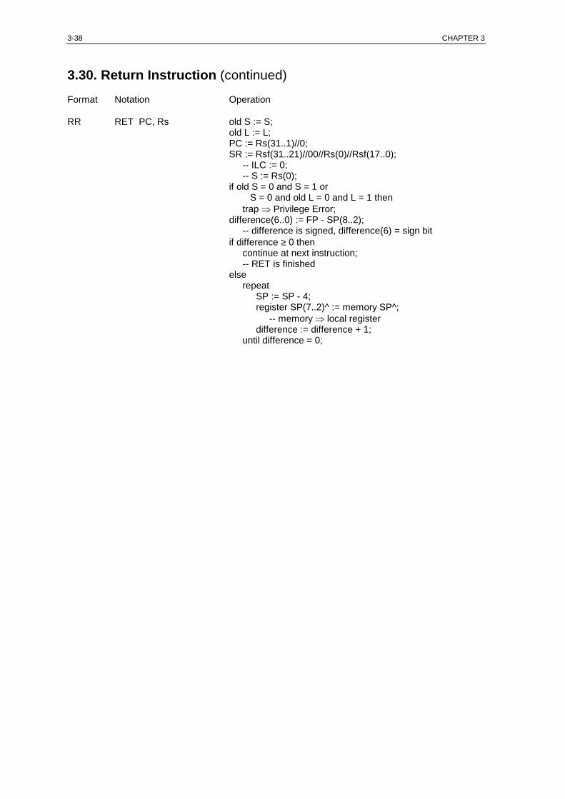
3-38 CHAPTER 3
3.30. Return Instruction (continued) Format Notation Operation
RR RET PC, Rs old S := S; old L := L; PC := Rs(31..1)//0; SR := Rsf(31..21)//00//Rs(0)//Rsf(17..0); -- ILC := 0; -- S := Rs(0); if old S = 0 and S = 1 or S = 0 and old L = 0 and L = 1 then trap ⇒ Privilege Error; difference(6..0) := FP - SP(8..2); -- difference is signed, difference(6) = sign bit if difference ≥ 0 then continue at next instruction; -- RET is finished else repeat SP := SP - 4; register SP(7..2)^ := memory SP^; -- memory ⇒ local register difference := difference + 1; until difference = 0;
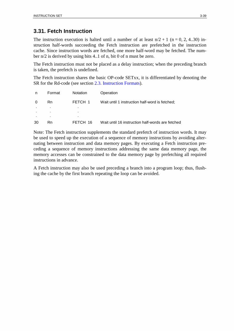
INSTRUCTION SET 3-39
3.31. Fetch Instruction The instruction execution is halted until a number of at least n/2 + 1 (n = 0, 2, 4..30) in-struction half-words succeeding the Fetch instruction are prefetched in the instruction cache. Since instruction words are fetched, one more half-word may be fetched. The num-ber n/2 is derived by using bits 4..1 of n, bit 0 of n must be zero.
The Fetch instruction must not be placed as a delay instruction; when the preceding branch is taken, the prefetch is undefined.
The Fetch instruction shares the basic OP-code SETxx, it is differentiated by denoting the SR for the Rd-code (see section 2.3. Instruction Formats).
n Format Notation Operation
0 Rn FETCH 1 Wait until 1 instruction half-word is fetched; . . . . . . . . .
30 Rn FETCH 16 Wait until 16 instruction half-words are fetched
Note: The Fetch instruction supplements the standard prefetch of instruction words. It may be used to speed up the execution of a sequence of memory instructions by avoiding alter-nating between instruction and data memory pages. By executing a Fetch instruction pre-ceding a sequence of memory instructions addressing the same data memory page, the memory accesses can be constrained to the data memory page by prefetching all required instructions in advance.
A Fetch instruction may also be used preceding a branch into a program loop; thus, flush-ing the cache by the first branch repeating the loop can be avoided.

3-40 CHAPTER 3
3.32. Extended DSP Instructions The Extended DSP instructions use the on-chip multiply-accumulate unit. Single word re-sults always use register G15 as destination register, while double-word results are always placed in G14 and G15. The condition flags remain unchanged.
Format Notation Operation
LLext EMUL Ld, Ls G15 := Ld * Ls; -- signed or unsigned multiplication, single word product
LLext EMULU Ld, Ls G14//G15 := Ld * Ls; -- unsigned multiplication, double word product
LLext EMULS Ld, Ls G14//G15 := Ld * Ls; -- signed multiplication, double word product
LLext EMAC Ld, Ls G15 := G15 + Ld * Ls; -- signed multiply/add, single word product sum
LLext EMACD Ld, Ls G14//G15 := G14//G15 + Ld * Ls; -- signed multiply/add, double word product sum
LLext EMSUB Ld, Ls G15 := G15 - Ld * Ls; -- signed multiply/subtract, single word product difference
LLext EMSUBD Ld, Ls G14//G15 := G14//G15 - Ld * Ls; -- signed multiply/subtract, double word product difference
LLext EHMAC Ld, Ls G15 := G15 + Ld(31..16) * Ls(31..16) + Ld(15..0) * Ls(15..0); -- signed half-word multiply/add, single word product sum
LLext EHMACD Ld, Ls G14//G15 := G14//G15 + Ld(31..16) * Ls(31..16) + Ld(15..0) * Ls(15..0); -- signed half-word multiply/add, double word product sum
LLext EHCMULD Ld, Ls G14 := Ld(31..16) * Ls(31..16) - Ld(15..0) * Ls(15..0); G15 := Ld(31..16) * Ls(15..0) + Ld(15..0) * Ls(31..16); -- half-word complex multiply
LLext EHCMACD Ld, Ls G14 := G14 + Ld(31..16) * Ls(31..16) - Ld(15..0) * Ls(15..0); G15 := G15 + Ld(31..16) * Ls(15..0) + Ld(15..0) * Ls(31..16); -- half-word complex multiply/add
LLext EHCSUMD Ld, Ls G14(31..16) := Ld(31..16) + G14; G14(15..0) := Ld(15..0) + G15; G15(31..16) := Ld(31..16) - G14; G15(15..0) := Ld(15..0) - G15; -- half-word (complex) add/subtract -- Ls is not used and should denote the same register as Ld
LLext EHCFFTD Ld, Ls G14(31..16) := Ld(31..16) + (G14 >> 15); G14(15..0) := Ld(15..0) + (G15 >> 15); G15(31..16) := Ld(31..16) - (G14 >> 15); G15(15..0) := Ld(15..0) - (G15 >> 15); -- half-word (complex) add/subtract with fixed-point adjustment -- Ls is not used and should denote the same register as Ld
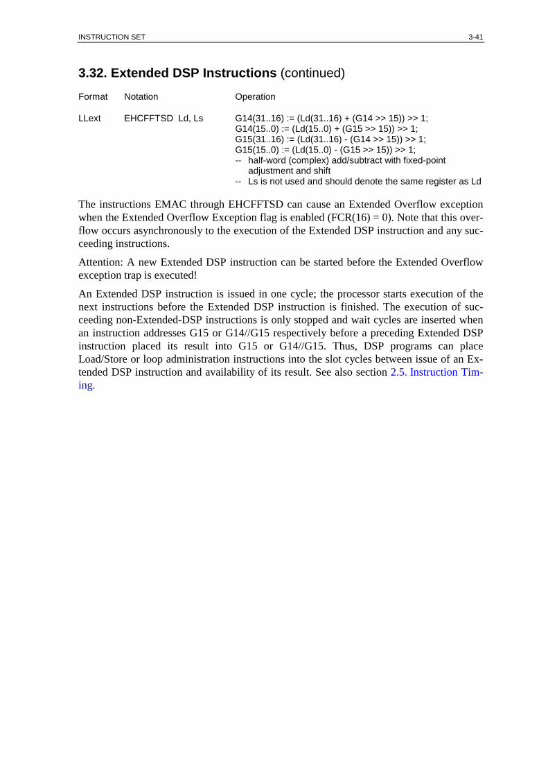
INSTRUCTION SET 3-41
3.32. Extended DSP Instructions (continued) Format Notation Operation
LLext EHCFFTSD Ld, Ls G14(31..16) := (Ld(31..16) + (G14 >> 15)) >> 1; G14(15..0) := (Ld(15..0) + (G15 >> 15)) >> 1; G15(31..16) := (Ld(31..16) - (G14 >> 15)) >> 1; G15(15..0) := (Ld(15..0) - (G15 >> 15)) >> 1; -- half-word (complex) add/subtract with fixed-point adjustment and shift -- Ls is not used and should denote the same register as Ld
The instructions EMAC through EHCFFTSD can cause an Extended Overflow exception when the Extended Overflow Exception flag is enabled (FCR(16) = 0). Note that this over-flow occurs asynchronously to the execution of the Extended DSP instruction and any suc-ceeding instructions.
Attention: A new Extended DSP instruction can be started before the Extended Overflow exception trap is executed!
An Extended DSP instruction is issued in one cycle; the processor starts execution of the next instructions before the Extended DSP instruction is finished. The execution of suc-ceeding non-Extended-DSP instructions is only stopped and wait cycles are inserted when an instruction addresses G15 or G14//G15 respectively before a preceding Extended DSP instruction placed its result into G15 or G14//G15. Thus, DSP programs can place Load/Store or loop administration instructions into the slot cycles between issue of an Ex-tended DSP instruction and availability of its result. See also section 2.5. Instruction Tim-ing.

3-42 CHAPTER 3
3.33. Software Instructions The Software instructions cause a branch to the subprogram associated with each Software instruction. Its entry address (see section 2.4. Entry Tables), deduced from the OP-code of the Software instruction, is placed in the program counter PC. Data is saved in the register sequence beginning at register address FP + FL (FL = 0 is interpreted as FL = 16) in as-cending order as follows:
Stack address of the destination operand
High-order word of the source operand
Low-order word of the source operand
Old program counter PC, containing the return address and the old S flag in bit zero
Old status Register SR, ILC contains the instruction-length code (ILC = 1) of the soft-ware instruction
Then the frame pointer FP is incremented by the old frame length FL and FL is set to six, thus creating a new stack frame. The cache-mode flag M and the trace-mode flag T are cleared, the interrupt-lock flag L is set to one. All condition flags remain unchanged.
Instruction execution then proceeds at the entry address placed in the PC.
Ls or Lsf and Ld may denote the same register.
Format Notation Operation
LL see specific if (trap table in Mem3) then instructions PC := 23 ones//0//OP(11..8)//4 zeros; else PC = MCR(13..12)//21 zeros//1//~OP(11..8)//1100; (FP + FL)^ := stack address of Ld; (FP + FL + 1)^ := Ls; (FP + FL + 2)^ := Lsf; (FP + FL + 3)^ := old PC(31..1)//old S; (FP + FL + 4)^ := old SR; FP := FP + FL; -- FL = 0 is treated as FL = 16 FL := 6; M := 0; T := 0; L := 1;
Note: At the new stack frame, the stack address of the destination operand can be ad-dressed as L0, the source operand as L1//L2, the saved PC as L3 and the saved SR as L4; L5 is free for use as required.
A Frame instruction must be executed before executing any other Software instruction, Trap or Call instruction or before the interrupt-lock flag L is being cleared, otherwise the beginning of the register part of the stack at SP could be overwritten without any warning.
INSTRUCTION SET 3-43
3.33.1. Do Instruction The Do instruction is executed as a Software instruction. The associated subprogram is entered, the stack address of the destination operand and one double-word source operand are passed to it (see section 3.33. Software Instructions for details).
The half-word succeeding the Do instruction will be used by the associated subprogram to differentiate branches to subordinate routines; the associated subprogram must increment the saved return program counter PC by two.
Format Notation Operation
LL DO xx... Ld, Ls execute Software instruction;
"xx..." stands for the mnemonic of the differentiating half-word after the OP-code of the Do instruction.
The Do instruction must not be placed as delay instruction since then xx... cannot be lo-cated.
Note: The Do instruction provides very code efficient passing of parameters to routines executing software implemented extensions of the instruction set.
Branching to unimplemented subordinate routines with the interrupt-lock flag L set to one must be excluded by bounds checks of the differentiating half-word at runtime; out-of-range values cannot be securely excluded at the assembly level.
The L flag must be cleared when the execution of a subordinate routine exceeds the regular interrupt latency time.
Application Note: The definition of subprograms entered via the Do instruction is reserved for system implementations. The values assigned to the differentiating half-word xx... after the OP-code of the Do instruction must be in ascending and contiguous order, starting with zero. This order enables fast range checking for an upper bound and also avoids unused space in the differentiating branch table.
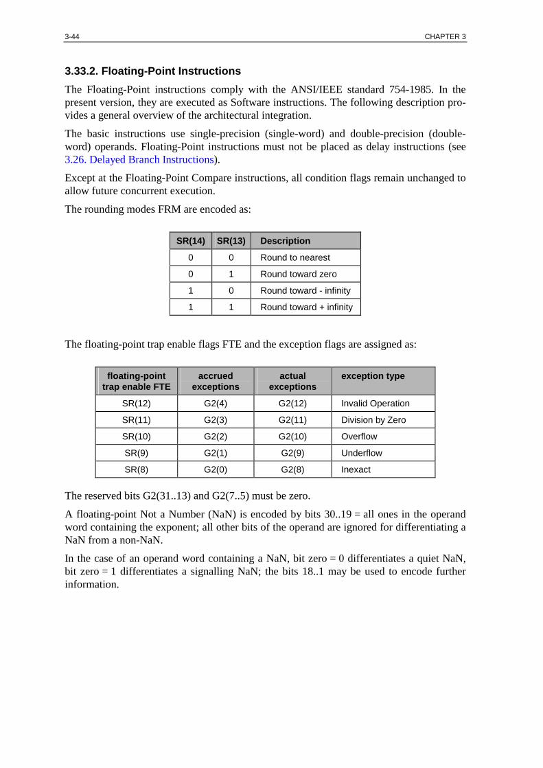
3-44 CHAPTER 3
3.33.2. Floating-Point Instructions The Floating-Point instructions comply with the ANSI/IEEE standard 754-1985. In the present version, they are executed as Software instructions. The following description pro-vides a general overview of the architectural integration.
The basic instructions use single-precision (single-word) and double-precision (double-word) operands. Floating-Point instructions must not be placed as delay instructions (see 3.26. Delayed Branch Instructions).
Except at the Floating-Point Compare instructions, all condition flags remain unchanged to allow future concurrent execution.
The rounding modes FRM are encoded as:
SR(14) SR(13) Description
0 0 Round to nearest
0 1 Round toward zero
1 0 Round toward - infinity
1 1 Round toward + infinity
The floating-point trap enable flags FTE and the exception flags are assigned as:
floating-point trap enable FTE
accrued exceptions
actual exceptions
exception type
SR(12) G2(4) G2(12) Invalid Operation
SR(11) G2(3) G2(11) Division by Zero
SR(10) G2(2) G2(10) Overflow
SR(9) G2(1) G2(9) Underflow
SR(8) G2(0) G2(8) Inexact
The reserved bits G2(31..13) and G2(7..5) must be zero.
A floating-point Not a Number (NaN) is encoded by bits 30..19 = all ones in the operand word containing the exponent; all other bits of the operand are ignored for differentiating a NaN from a non-NaN.
In the case of an operand word containing a NaN, bit zero = 0 differentiates a quiet NaN, bit zero = 1 differentiates a signalling NaN; the bits 18..1 may be used to encode further information.
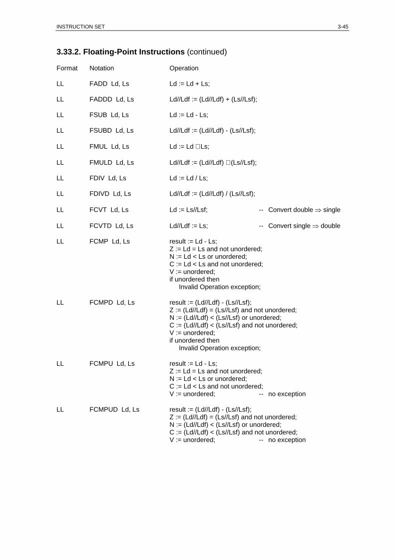
INSTRUCTION SET 3-45
3.33.2. Floating-Point Instructions (continued)
Format Notation Operation
LL FADD Ld, Ls Ld := Ld + Ls;
LL FADDD Ld, Ls Ld//Ldf := (Ld//Ldf) + (Ls//Lsf);
LL FSUB Ld, Ls Ld := Ld - Ls;
LL FSUBD Ld, Ls Ld//Ldf := (Ld//Ldf) - (Ls//Lsf);
LL FMUL Ld, Ls Ld := Ld ∗ Ls;
LL FMULD Ld, Ls Ld//Ldf := (Ld//Ldf) ∗ (Ls//Lsf);
LL FDIV Ld, Ls Ld := Ld / Ls;
LL FDIVD Ld, Ls Ld//Ldf := (Ld//Ldf) / (Ls//Lsf);
LL FCVT Ld, Ls Ld := Ls//Lsf; -- Convert double ⇒ single
LL FCVTD Ld, Ls Ld//Ldf := Ls; -- Convert single ⇒ double
LL FCMP Ld, Ls result := Ld - Ls; Z := Ld = Ls and not unordered; N := Ld < Ls or unordered; C := Ld < Ls and not unordered; V := unordered; if unordered then Invalid Operation exception;
LL FCMPD Ld, Ls result := (Ld//Ldf) - (Ls//Lsf); Z := (Ld//Ldf) = (Ls//Lsf) and not unordered; N := (Ld//Ldf) < (Ls//Lsf) or unordered; C := (Ld//Ldf) < (Ls//Lsf) and not unordered; V := unordered; if unordered then Invalid Operation exception;
LL FCMPU Ld, Ls result := Ld - Ls; Z := Ld = Ls and not unordered; N := Ld < Ls or unordered; C := Ld < Ls and not unordered; V := unordered; -- no exception
LL FCMPUD Ld, Ls result := (Ld//Ldf) - (Ls//Lsf); Z := (Ld//Ldf) = (Ls//Lsf) and not unordered; N := (Ld//Ldf) < (Ls//Lsf) or unordered; C := (Ld//Ldf) < (Ls//Lsf) and not unordered; V := unordered; -- no exception

3-46 CHAPTER 3
3.33.2. Floating-Point Instructions (continued) A floating-point instruction, except a Floating-point Compare, can raise any of the excep-tions Invalid Operation, Division by Zero, Overflow, Underflow or Inexact. FCMP and FCMPD can raise only the Invalid Operation exception (at unordered). FCMPU and FCMPUD cannot raise any exception.
At an exception, the following additional action is performed:
Any corresponding accrued-exception flag whose corresponding trap-enable flag is zero (not enabled) is set to one; all other accrued-exception flags remain unchanged.
If a corresponding trap-enable flag is one (enabled), any corresponding actual-exception flag is set to one; all other actual-exception flags are cleared. The destination remains unchanged. In the present software version, the software emulation routine must branch to the corre-sponding user-supplied exception trap handler. The (modified) result, the source oper-and, the stack address of the destination operand and the address of the floating-point instruction are passed to the trap handler. In the future hardware version, a trap to Range Error will occur; the Range Error handler will then initiate re-execution of the floating-point instruction by branching to the entry of the corresponding software emulation rou-tine, which will then act as described before.
The only exceptions that can coincide are Inexact with Overflow and Inexact with Under-flow. An Overflow or Underflow trap, if enabled, takes precedence over an Inexact trap; the Inexact accrued-exception flag G2(0) must then be set as well.

INSTRUCTION SET 3-47
3.33.2. Floating-Point Instructions (continued) The table below shows the combinations of Floating-Point Compare and Branch in-structions to test all 14 floating-point relations:
relation Compare Branch on true
Branch on false
exception if unordered
= FCMPU BE BNE --
?≠ FCMPU BNE BE --
> FCMP BGT BLE x
≥ FCMP BGE BLT x
< FCMP BLT BGE x
≤ FCMP BLE BGT x
? FCMPU BV BNV --
≠ FCMP BNE BE x
<=> FCMP -- -- x
?> FCMPU BHT BSE --
?≥ FCMPU BHE BST --
?< FCMPU BLT BGE --
?≤ FCMPU BLE BGT --
?= FCMPU BE, BV BST, BGT --
The symbol ? signifies unordered.
Note: At the test <=> (ordered), no branch after FCMP is required since the result of the test is an Invalid Operation exception occurred or not occurred.

3-48 CHAPTER 3
This page is intentionally left blank.
EXCEPTIONS 4-1
4. Exceptions
4.1. Exception ProcessingExceptions are events which redirect the flow of control to a supervisor subprogram asso-ciated with the type of exception, that is, a trap occurs as a response to the exception. (Seea detailed description of exceptions further below.) If exceptions coincide, the exceptionwith the highest priority takes precedence over all exceptions with lower priority.
Processing of an exception proceeds as follows:
The entry address (see section 2.4. Entry Tables) of the associated subprogram is placed inthe program counter PC and the supervisor-state flag S is set to one. The old PC is saved inthe register addressed by FP + FL; the old S flag is also saved in bit zero of this register.The old status register SR is saved in the register addressed by FP + FL + 1 (FL = 0 is in-terpreted as FL = 16); the saved instruction-length code ILC contains (in general, see sec-tion 4.3. Exception Backtracking). the instruction-length code of the preceding instruction.
Then the frame pointer FP is incremented by the old frame length FL and FL is set to two,thus creating a new stack frame. The cache-mode flag M and the trace-mode flag T arecleared, the interrupt-lock flag L is set to one. All condition flags remain unchanged.
Operation
PC := entry address of exception subprogram;S := 1;(FP + FL)^ := old PC(31..1)//old S;(FP + FL + 1)^ := old SR;FP := FP + FL; -- FL = 0 is treated as FL = 16FL := 2;M := 0;T := 0;L := 1;
Note: At the new stack frame, the saved PC can be addressed as L0 and the saved SR asL1. Since FL = 2, no other local registers are free for use.
A Frame instruction must be executed before the interrupt-lock flag L is cleared, before anyCall, Trap, Software instruction or any instruction with the potential to cause an exceptionis executed. Otherwise, the beginning of the register part of the stack at the SP could beoverwritten without any warning.
An entry caused by an exception can be differentiated from an entry caused by a Trap in-struction by the value of FL: FL is set to two by an exception and set to six by a Trap in-struction.

4-2 CHAPTER 4
4.2. Exception TypesThe following exception are types ordered by priorities, Reset has the highest priority. Incase of coincidental exceptions, higher-priority exceptions overrule lower-priority excep-tions.
4.2.1. ResetA Reset exception occurs on a transition of the RESET# signal from low to high or as aresult of a watchdog overrun in IO3 Watchdog mode or after a reset following a clock-down command. The Reset exception overrules all other exceptions and is used to startexecution at the Reset entry.
The load and store pipelines are cleared. The BCR, MCR, FCR and TPR initialization inthe three reset cases is specified in the table 4.1; all other registers and flags, except thoseset or cleared explicitly by the exception processing itself, remain undefined and must beinitialized by software.
In the reset handler, ISR bits 9 and 10 can be used to discriminate between the three resetsources.
Reset source BCR MCR FCR TPR
RESET# initialized initialized initialized initialized
Watchdog initialized initialized initialized preserved
Clock-Down initialized initialized preserved initialized
Table 4.1: BCR, MCR, FCR, TPR initialization on Reset
The FCR is preserved on a clock-down reset in order to have the correct interrupt mask andpolarity for the wakeup from clock-down. TPR is preserved on a watchdog reset to allowthe use of the watchdog reset as a controlled time-out without losing the time base. Theother registers are initialized to their specific reset value.
Note: The frame pointer FP can only be set to a defined value by restoring it from the FP inthe return SR through a Return instruction.
4.2.2. Range, Pointer, Frame and Privilege ErrorThese exceptions share a common entry since they cannot occur coincidentally at the sameinstruction. The error-causing instruction can be identified by backtracking.
A Range Error exception occurs when an operand or result exceeds its value range.
A Pointer Error is caused by an attempted memory access using an address register (Rd orLd) with the content zero. The memory is not accessed, but the content of the address reg-ister is updated in case of a post-increment or next address mode.
A Frame Error occurs when the restructuring of the stack frame reaches or exceeds the up-per bound UB of the memory part of the stack. No further Frame instruction must be exe-cuted by the error routine for Pointer, Frame and Privilege Error before the UB is set to ahigher value and thus, an expanded stack frame fits into the higher stack bound.
A Privilege Error occurs when a privileged operation is executed in user or on return touser state (see section 1.5. Privilege States for details).

EXCEPTIONS 4-3
4.2.3. Extended OverflowAn Extended Overflow condition is raised on an overflow caused by an add or subtractoperation as part of the execution of one of the Extended instructions EMAC throughEHCFFTSD when the Extended Overflow exception is enabled. The Extended Overflowexception is enabled by clearing bit 16 of the function control register FCR to zero.
When the Extended Overflow exception is blocked by a higher-priority exception or by theL flag being set, the Extended Overflow condition is saved internally; the exception trapoccurs then when the blocking is released.
The Extended Overflow condition is cleared by the exception trap or by setting FCR(16) toone (disabled).
The Extended Overflow exception trap occurs asynchronously to the causing instruction;thus, the causing instruction cannot be identified by backtracking. Usually, there is onlyone instruction in a loop which can cause an Extended Overflow exception; thus, a handlercan identify that instruction. When a second Extended Overflow condition is raised beforethe first one caused a trap, it is ored and only one trap is taken.
4.2.4. Parity ErrorA Parity Error exception can be enabled individually for each of the memory areasMEM0..MEM3. When enabled, a parity error on an access to the corresponding memoryarea causes a Parity Error exception.
When the Parity Error exception is blocked by a higher-priority exception or by the L flagbeing set, the Parity Error condition is saved internally, the exception trap occurs thenwhen the blocking is released.
The Parity Error condition is cleared only by the exception trap; it is not cleared by settingany of the disable bits 31..28 in the BCR after a Parity Error condition is saved internally.
The Parity Error exception trap occurs asynchronously to the causing memory instruction.Since memory accesses are pipelined, a Parity Error exception cannot be related to a spe-cific memory instruction.
4.2.5. InterruptAn Interrupt exception is caused by an external interrupt signal, by the timer interrupt or byan IO3 Control Mode. Since the interrupt-lock flag L is set by the exception processing, nofurther interrupts can occur until the L flag is cleared. The interrupt exception processingsets also the interrupt-mode flag I to one. See also sections 2.4. Entry Tables, 5. Timer andCPU Clock Modes and 6.9. Bus Signals.
The I flag is used by the operating system, it must not be cleared by the interrupt handler. AReturn instruction restores the old value from the saved SR automatically.
4-4 CHAPTER 4
4.2.6. Trace ExceptionA Trace exception occurs after each execution of an instruction except a Delayed Branchinstruction when the trace mode is enabled (trace flag T = 1) and the trace pending flag P isone. After a Call instruction, a Trace exception is suppressed until the next instruction isexecuted regardless of the trace mode being enabled; the T flag is not affected.
The P flag in the saved return status register SR must be cleared by the trace handler toprevent tracing the same instruction again.
The instruction preceding the Trace exception cannot be backtracked since only potentiallyerror-causing instructions can and need be backtracked.
4.3. Exception BacktrackingIn the case of a Pointer, Frame, Privilege and Range Error exception caused by a delay in-struction succeeding a delayed branch taken, the location of the saved PC contains the ad-dress of the delay instruction and the saved instruction length code ILC contains the lengthof the Delayed Branch instruction (in half-words).
In the case of all other exceptions, the location of the saved PC contains the return address,that is, the address of the instruction which would have been executed next if the exceptionhad not occurred. The saved ILC contains the length of the last instruction except when thelast instruction executed was a branch taken; a Return instruction clears the ILC and thus,the saved ILC after a Return instruction contains zero.
An exception caused by a Pointer, Frame, Privilege or Range Error, except following aReturn instruction, can be backtracked. For backtracking, the content of the adjusted savedILC is subtracted from the address contained in the location of the saved PC.
If the backtrack-address calculated in this way points to a Delayed Branch instruction, theerror-causing instruction is a delay instruction with a preceding delayed branch taken andthe address contained in the location of the saved PC points to the address of this delayinstruction.
If the backtrack-address calculated does not point to a Delayed Branch instruction, it pointsdirectly to the error-causing instruction. This instruction is then either not a delay instruc-tion or a delay instruction with the preceding delayed branch not taken.
The error-causing instruction can then be inspected and the cause of an error analyzed indetail.
In the case of a Privilege Error, the ILC must be tested for zero to single out an exceptioncaused by a Return instruction before backtracking. Thus, an exception caused by a Returninstruction can be identified. However, it cannot be backtracked to the instruction addressof the Return instruction because the return address saved does not succeed the address ofthe Return instruction. All other branching instructions cannot be backtracked either. Sincethese instructions cause no errors, backtracking is not required.
EXCEPTIONS 4-5
The stack address of a local register denoted by a backtracked instruction can be calculatedaccording to the following formula:
stack address of preceding stack frame := stack address ofcurrent stack frame - (((FP - saved FP) modulo 64) * 4);
-- bits 5..0 of the difference (FP - saved FP) are used zero-expanded-- * 4 converts word difference ⇒ byte difference-- the stack address of the current stack frame is provided by the
Set Stack Address instructionstack address of local register := stack address of precedingstack frame + (local register address code * 4);
-- * 4 converts local register word offset ⇒ byte offset
Note: Backtracking allows a much more detailed analysis of error causes than a more dif-ferentiated trapping could provide. Exception handlers can get more information abouterror causes and the precise messages required by most programming languages can beeasily generated.

4-6 CHAPTER 4
This page is intentionally left blank.

TIMER 5-1
5. Timer and CPU Clock Modes
5.1. OverviewThe on-chip timer is controlled via three registers:
Timer prescaler register TPR G21
Timer register TR G23
Timer compare register TCR G22
The timer prescaler register also controls the processor clock output of the PLL circuit.
G21..G23 can be addressed only via the high global flag H by a MOV or MOVI instruc-tion. The content of G21 (timer prescaler register) cannot be read.
Additionally, two different power saving modes are implemented: power-down mode andsleep mode (clock-down mode).
5.1.1. Timer Prescaler Register TPRGlobal register G21 is the write-only Timer Prescaler Register TPR. The TPR adapts thetimer clock to different processor clock frequencies and controls the PLL clock output.
Bits 26 to 28 select the processor clock. Bits 23..16 determine the basic time unit viafrequency of timer clock = frequency of processor clock divided by (n+2)
n is the value of bits 23..16, n is in the range from 0 to 255 yielding division factors from 2to 257. Given a basic time unit, n can be calculated as
n = (time unit * frequency of processor clock) - 2.
Bit 31 determines the effect of a write to TPR. If bit 31 is 0, a write to TPR takes effectimmediately, the processor clock divider is changed and the timer prescaler divider is re-loaded. If bit 31 is 1, the processor clock divider and timer prescaler divider update is de-layed until the current basic time unit ends. At the end of the current time unit, the proces-sor clock divider and the timer prescaler divider are updated with the new values. This al-lows keeping absolute timing even when the processor clock is changed by simultaneouslychanging the processor clock divider and the timer prescaler divider.
The TPR is initialized to bit 28=0, 27..26=1, and 23..16=0 on reset (from the RESET# pinor by a Clock-Down reset), i.e. the processor starts with CPU clock = XTAL1 clock, theprescaler divides by 2. During a Watchdog (IO3 Timer) Reset, the TPR is preserved. Thisallows the use of the Watchdog as a controlled time-out without losing the time base.
Bits 30..29, 25..24 and 15..0 are reserved and must be zero on a move to TPR.
The processor clock divider control can be used to slow down the CPU clock in order tosave power during times when only a part of the processing power of the CPU is needed.Whenever the full processing power is needed, the CPU clock can be switched back to fullspeed.

5-2 CHAPTER 5
Bits Name Description
31 LoadEnable 1 = TPR update is delayed until current prescaler time unit ends0 = TPR update is performed immediately
30..29 reserved
28..26 ClockDivider CPU Clock Divider Control111 = reserved110 = reserved101 = reserved100 = CPU clock = XTAL1 clock / 2011 = CPU clock = XTAL1 clock010 = CPU clock = XTAL1 clock * 2001 = CPU clock = XTAL1 clock * 4000 = CPU clock = XTAL1 clock * 8
25..24 reserved
23..16 TimerPrescaler Timer Prescaler Division factor nRange n = 0..255, Timer Prescaler divides by n+2
15..0 reserved
Table 5.1: Timer Prescaler Register TPR
5.1.2. Timer Register TRThe TR is a 32-bit register which is incremented by one on each time unit modulo 232. Itscontent can be used as the lower word of a double-word integer, representing the time in-clusive date.
The TPR and the TR should be set only once on system initialization, whereby the follow-ing instruction sequence must be observed strictly (interrupts must be locked out): : : FETCH 4 ORI SR, $20 ; set H-flag MOV TPR, Lx ; load prescaler register from local register x ORI SR, $20 ; set H-flag MOV TR, Ly ; load timer register from local register y : :
Note: The Fetch instruction is necessary to prevent insertion of idle cycles during the pre-scribed instruction sequence.
TIMER 5-3
5.1.3. Timer Compare Register TCRThe content of the TCR is compared continuously with the content of the timer register TR.An unsigned modulo comparison is performed according to:
result(31..0) := TR(31..0) - TCR(31..0)
On result(31) = 0, the TR is higher than or equal to the TCR.
When the timer interrupt is enabled (FCR(23) = 0) and the value in the TR is higher than orequal to the value in the TCR, a timer interrupt is generated. This interrupt is cleared byloading the TCR with a value higher than the current content of the TR.
Timer interrupts can be masked out by FCR(23) = 1; FCR(23) is set to one on Reset. Thetimer interrupt disable bit FCR(23) does not affect the timer and compare function.
A delay time in the TCR is calculated according to the formula:TCR := current content of TR + number of delay time units
The maximum number of delay time units allowed for this calculation is 231-1.
For example:
TR(31..0) = hex FFFF FF00
delay time units (= 1000) = hex 0000 03E8
TCR(31..0) = hex 0000 02E8
Since the modulo comparison is an unsigned operation, only unsigned arithmetic must beused for calculations with timer and timer compare values. Do not use the N or C flag totest for the result of the comparison TR - TCR, use only result bit 31!
5.1.4. Power-Down ModeWhen the power-down mode is entered, the execution pipeline of the processor is halted.Only the logic for the timer, IO3 control modes, interrupt and refresh is being clocked, allother clocks are disabled. The processor is temporarily activated for refresh and bus arbi-tration cycles, no instructions are executed during these temporary clock cycles. The proc-essor resumes execution by any interrupt or on a reset.
Power-down mode can be entered by executing an I/O write instruction with address bitsA(27) and A(25..23) set to one and A(22) set to zero.
When power-down mode is entered via the I/O write instruction, the power-down modetakes effect at the time when the I/O access is performed. Until this time, instruction exe-cution continues. To ensure that the power-down mode takes effect, the power-down I/Oaccess must be followed by a dummy I/O load accesses to the same address with 2 accessand 2 hold cycles. A following dependent instruction then waits until both I/O accesses areperformed. Thus, instructions following the MOV instruction are not executed untilwakeup. Note that even though the power-down request is an internal operation of theprocessor, bus grant must be given so that the power-down I/O access can be performed.

5-4 CHAPTER 5
Power-down mode can be set by a program sequence as in the following example:PowerDownIO EQU 1 << 27 | %1110 << 22 ; Bits 27, 25..23, 22
... STW.IOA 0, 0, PowerDownIO ; set power-down mode LDW.IOA 0, L4, PowerDownIO | 8 ; wait until power-down MOV L4, L4 ; I/O is executed ... ; execution continues
; here after wakeup
5.1.5. Additional Power SavingThe CPU clock divider control can be used for example to switch the CPU to a slow clockduring power-down for additional power savings. In the following example, the XTAL1clock is 10 MHz, the CPU runs at 80 MHz and is switched back to 10 MHz during power-down. The timer prescaler setting is changed so that a time unit of 1 µs is kept through thepower-down sequence. Using the “delayed TPR update” feature, the 1 µs absolute time ismaintained even for the time units where the TPR setting changes.
Interrupts are locked out during power-down using the L bit in SR. This is done so that theTPR setting can be changed back to fast clock and corresponding prescaler setting afterwakeup from power-down before the interrupt handler is called. The interrupt occurs at thetime the lock bit L in SR is cleared.
The power-down is initiated by executing the power-down I/O access. The power-down isguaranteed to be effective before the next (dummy) I/O load access is done, thus the fol-lowing MOV instruction is not executed until wakeup. The instructions to restore the CPUclock speed and the prescaler setting can thus be placed after the dummy load and MOVinstructions.TPR_fast EQU %000 << 26 | 78 << 16 ; fast TPR, divide by 80TPR_slow EQU %011 << 26 | 8 << 16 ; slow TPR, divide by 10DelayTPRUpd EQU 1 << 31 ; delayed TPR updateL_Bit EQU 1 << 15 ; Interrupt Lock in SRH_Bit EQU 1 << 5 ; High-Global Bit in SRPowerDownIO EQU 1 << 27 | %1110 << 22 ; Power-Down I/O address
...
MOVI L5, TPR_slow ; TPR for power-down MOVI L6, TPR_fast ; TPR after power-down ORI L5, DelayTPRUpd ; set delayed TPR update ORI L6, DelayTPRUpd ; set delayed TPR update
ORI SR, L_Bit | H_Bit ; set Interrupt Lock MOV TPR, L5 ; set slow clock
STW.IOA 0, 0, PowerDownIO ; set power-down mode LDW.IOA 0, L4, PowerDownIO | 8 ; dummy load MOV L4, L4 ; wait till done
; next instruction is; executed after wakeup
ORI SR, H_Bit MOV TPR, L6 ; restore fast clock ANDNI SR, L_Bit ; allow interrupt now
... ; continue here after; interrupt routine has; been executed
TIMER 5-5
5.1.6. Sleep ModeTo further reduce power dissipation, the processor can be set into sleep mode. In this case,the clock of the processor is completely switched off. When a quartz crystal is used forprocessor clock generation, it is also switched off. An external reset signal or an interruptawakes the processor from sleep mode and the processor continues with the standard resetprocedure. Bit 10 in ISR indicates that the reset was caused by a wakeup from sleep mode.The sleep mode can be entered by an I/O write instruction with address bits A(27) andA(25..22) set to one. Note that any content of the internal RAM and the external DRAM aswell as the timer count will be lost during sleep mode.
The sleep mode takes effect when the I/O access is performed. After this, the processorbehaves as in reset, i.e. the bus request is deactivated until wakeup by an interrupt or reset.On wakeup by an interrupt, the FCR setting is preserved through the reset sequence. Aswith the power-down I/O access, a dummy load access could be placed after the sleepmode I/O access to ensure that the sleep mode takes effect. Since the processor continueswith a reset at wakeup from sleep mode, an empty loop can be used as well to wait until thesleep mode I/O access has taken effect. Note that even though sleep mode is an internaloperation of the processor, bus grant must be given so that the sleep mode set I/O accesscan be performed.
An interrupt signal awaking the processor from sleep mode must stay active at least untilthe processor has begun executing its reset sequence. This latency time includes the startuptime of the crystal oscillator and of the PLL circuit. If the interrupt goes inactive before thislatency time has elapsed, the processor may fall back into sleep mode. In order to have theeffect of causing a processor interrupt, the interrupt signal should stay active until it is ac-knowledged by the interrupt handler.
The sleep mode can be set by a program sequence as in the following example:SleepModeIO EQU 1 << 27 | %1111 << 22 ; Bits 27, 25..22
... STW.IOA 0, 0, SleepModeIO ; set sleep mode
SleepWait: BR SleepWait ; wait until sleep ; mode I/O is executed

5-6 CHAPTER 5
This page is intentionally left blank.
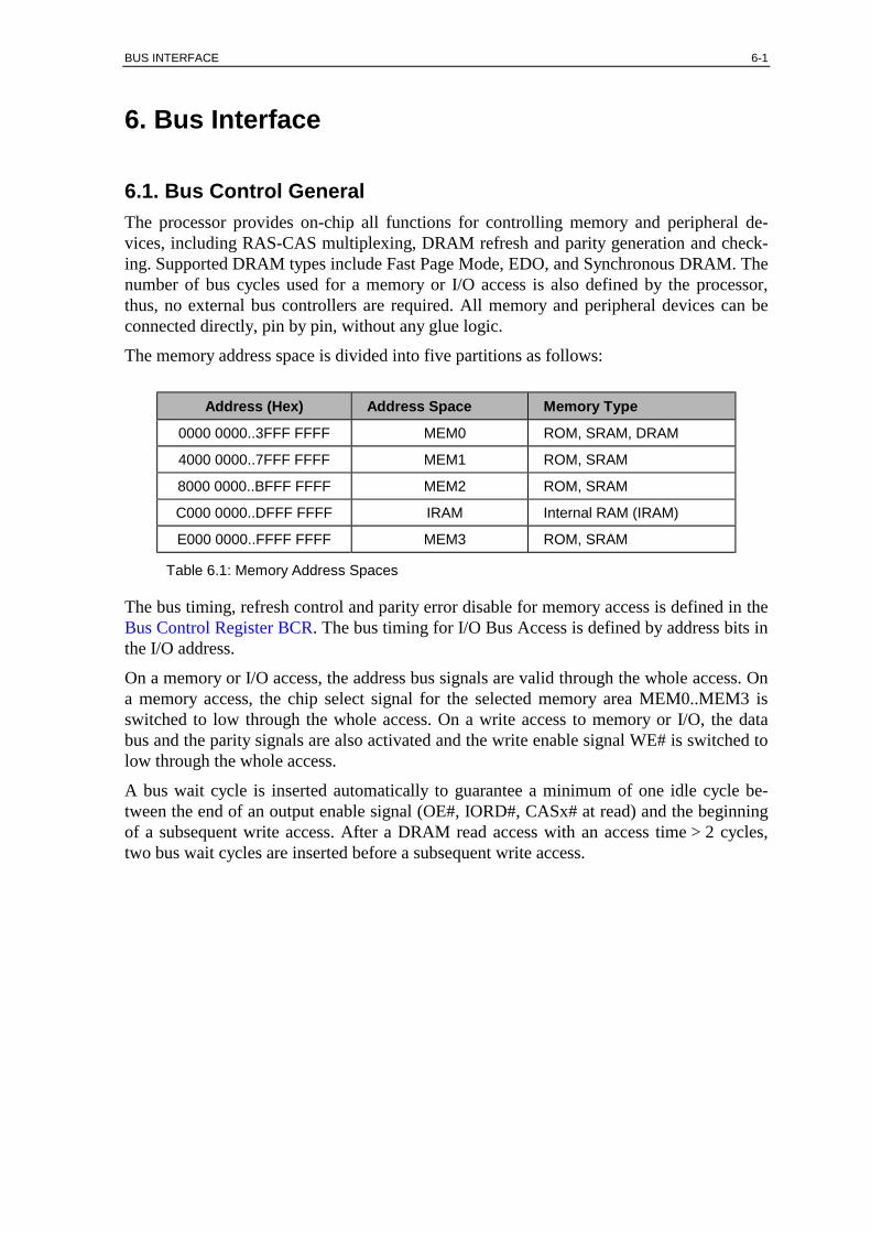
BUS INTERFACE 6-1
6. Bus Interface
6.1. Bus Control GeneralThe processor provides on-chip all functions for controlling memory and peripheral de-vices, including RAS-CAS multiplexing, DRAM refresh and parity generation and check-ing. Supported DRAM types include Fast Page Mode, EDO, and Synchronous DRAM. Thenumber of bus cycles used for a memory or I/O access is also defined by the processor,thus, no external bus controllers are required. All memory and peripheral devices can beconnected directly, pin by pin, without any glue logic.
The memory address space is divided into five partitions as follows:
Address (Hex) Address Space Memory Type
0000 0000..3FFF FFFF MEM0 ROM, SRAM, DRAM
4000 0000..7FFF FFFF MEM1 ROM, SRAM
8000 0000..BFFF FFFF MEM2 ROM, SRAM
C000 0000..DFFF FFFF IRAM Internal RAM (IRAM)
E000 0000..FFFF FFFF MEM3 ROM, SRAM
Table 6.1: Memory Address Spaces
The bus timing, refresh control and parity error disable for memory access is defined in theBus Control Register BCR. The bus timing for I/O Bus Access is defined by address bits inthe I/O address.
On a memory or I/O access, the address bus signals are valid through the whole access. Ona memory access, the chip select signal for the selected memory area MEM0..MEM3 isswitched to low through the whole access. On a write access to memory or I/O, the databus and the parity signals are also activated and the write enable signal WE# is switched tolow through the whole access.
A bus wait cycle is inserted automatically to guarantee a minimum of one idle cycle be-tween the end of an output enable signal (OE#, IORD#, CASx# at read) and the beginningof a subsequent write access. After a DRAM read access with an access time > 2 cycles,two bus wait cycles are inserted before a subsequent write access.
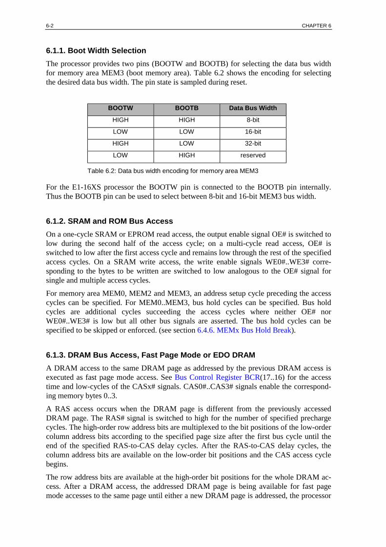
6-2 CHAPTER 6
6.1.1. Boot Width SelectionThe processor provides two pins (BOOTW and BOOTB) for selecting the data bus widthfor memory area MEM3 (boot memory area). Table 6.2 shows the encoding for selectingthe desired data bus width. The pin state is sampled during reset.
BOOTW BOOTB Data Bus Width
HIGH HIGH 8-bit
LOW LOW 16-bit
HIGH LOW 32-bit
LOW HIGH reserved
Table 6.2: Data bus width encoding for memory area MEM3
For the E1-16XS processor the BOOTW pin is connected to the BOOTB pin internally.Thus the BOOTB pin can be used to select between 8-bit and 16-bit MEM3 bus width.
6.1.2. SRAM and ROM Bus AccessOn a one-cycle SRAM or EPROM read access, the output enable signal OE# is switched tolow during the second half of the access cycle; on a multi-cycle read access, OE# isswitched to low after the first access cycle and remains low through the rest of the specifiedaccess cycles. On a SRAM write access, the write enable signals WE0#..WE3# corre-sponding to the bytes to be written are switched to low analogous to the OE# signal forsingle and multiple access cycles.
For memory area MEM0, MEM2 and MEM3, an address setup cycle preceding the accesscycles can be specified. For MEM0..MEM3, bus hold cycles can be specified. Bus holdcycles are additional cycles succeeding the access cycles where neither OE# norWE0#..WE3# is low but all other bus signals are asserted. The bus hold cycles can bespecified to be skipped or enforced. (see section 6.4.6. MEMx Bus Hold Break).
6.1.3. DRAM Bus Access, Fast Page Mode or EDO DRAMA DRAM access to the same DRAM page as addressed by the previous DRAM access isexecuted as fast page mode access. See Bus Control Register BCR(17..16) for the accesstime and low-cycles of the CASx# signals. CAS0#..CAS3# signals enable the correspond-ing memory bytes 0..3.
A RAS access occurs when the DRAM page is different from the previously accessedDRAM page. The RAS# signal is switched to high for the number of specified prechargecycles. The high-order row address bits are multiplexed to the bit positions of the low-ordercolumn address bits according to the specified page size after the first bus cycle until theend of the specified RAS-to-CAS delay cycles. After the RAS-to-CAS delay cycles, thecolumn address bits are available on the low-order bit positions and the CAS access cyclebegins.
The row address bits are available at the high-order bit positions for the whole DRAM ac-cess. After a DRAM access, the addressed DRAM page is being available for fast pagemode accesses to the same page until either a new DRAM page is addressed, the processor
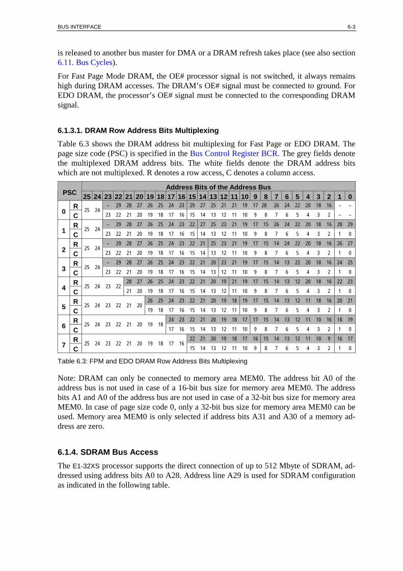
BUS INTERFACE 6-3
is released to another bus master for DMA or a DRAM refresh takes place (see also section6.11. Bus Cycles).
For Fast Page Mode DRAM, the OE# processor signal is not switched, it always remainshigh during DRAM accesses. The DRAM’s OE# signal must be connected to ground. ForEDO DRAM, the processor’s OE# signal must be connected to the corresponding DRAMsignal.
6.1.3.1. DRAM Row Address Bits Multiplexing
Table 6.3 shows the DRAM address bit multiplexing for Fast Page or EDO DRAM. Thepage size code (PSC) is specified in the Bus Control Register BCR. The grey fields denotethe multiplexed DRAM address bits. The white fields denote the DRAM address bitswhich are not multiplexed. R denotes a row access, C denotes a column access.
Address Bits of the Address BusPSC 25 24 23 22 21 20 19 18 17 16 15 14 13 12 11 10 9 8 7 6 5 4 3 2 1 0
R – 29 28 27 26 25 24 23 29 27 25 21 21 19 17 28 26 24 22 20 18 16 – –0 C
25 2423 22 21 20 19 18 17 16 15 14 13 12 11 10 9 8 7 6 5 4 3 2 – –
R – 29 28 27 26 25 24 23 22 27 25 23 21 19 17 15 26 24 22 20 18 16 28 291 C
25 2423 22 21 20 19 18 17 16 15 14 13 12 11 10 9 8 7 6 5 4 3 2 1 0
R – 29 28 27 26 25 24 23 22 21 25 23 21 19 17 15 14 24 22 20 18 16 26 272 C
25 2423 22 21 20 19 18 17 16 15 14 13 12 11 10 9 8 7 6 5 4 3 2 1 0
R – 29 28 27 26 25 24 23 22 21 20 23 21 19 17 15 14 13 22 20 18 16 24 253 C
25 2423 22 21 20 19 18 17 16 15 14 13 12 11 10 9 8 7 6 5 4 3 2 1 0
R 28 27 26 25 24 23 22 21 20 19 21 19 17 15 14 13 12 20 18 16 22 234 C
25 24 23 2221 20 19 18 17 16 15 14 13 12 11 10 9 8 7 6 5 4 3 2 1 0
R 26 25 24 23 22 21 20 19 18 19 17 15 14 13 12 11 18 16 20 215 C
25 24 23 22 21 2019 18 17 16 15 14 13 12 11 10 9 8 7 6 5 4 3 2 1 0
R 24 23 22 21 20 19 18 17 17 15 14 13 12 11 10 16 18 196 C
25 24 23 22 21 20 19 1817 16 15 14 13 12 11 10 9 8 7 6 5 4 3 2 1 0
R 22 21 20 19 18 17 16 15 14 13 12 11 10 9 16 177 C
25 24 23 22 21 20 19 18 17 1615 14 13 12 11 10 9 8 7 6 5 4 3 2 1 0
Table 6.3: FPM and EDO DRAM Row Address Bits Multiplexing
Note: DRAM can only be connected to memory area MEM0. The address bit A0 of theaddress bus is not used in case of a 16-bit bus size for memory area MEM0. The addressbits A1 and A0 of the address bus are not used in case of a 32-bit bus size for memory areaMEM0. In case of page size code 0, only a 32-bit bus size for memory area MEM0 can beused. Memory area MEM0 is only selected if address bits A31 and A30 of a memory ad-dress are zero.
6.1.4. SDRAM Bus AccessThe E1-32XS processor supports the direct connection of up to 512 Mbyte of SDRAM, ad-dressed using address bits A0 to A28. Address line A29 is used for SDRAM configurationas indicated in the following table.

6-4 CHAPTER 6
A31..A30 A29 A28 A27..A0 Function
00 0 address address SDRAM access
00 1 0 * set SDRAM Mode Register (from address bits)
00 1 1 * set SDRAM Control Register SDCR (from address bits)
Table 6.4: SDRAM memory and configuration access select
The address bits for the SDRAM bank addresses can be selected from address bits A20 toA28. The E1-32XS processor supports the generation of two SDRAM chip select signals sothat two SDRAM banks can be connected directly. The address bit that discriminates be-tween the two SDRAM chip selects can be selected from address bits A21 to A28. Thesecond SDRAM chip select signal is not available on the E1-16XS. See the SDRAM Con-trol Register description in section 6.5.
6.1.4.1. SDRAM Row Address Bits Multiplexing
For row access and column access, the address bits are multiplexed corresponding to theSDRAM address mapping table given below depending on the Page Size Code (PSC). At acolumn access, additional to the address bits in the column address range, the bank addressbits are also enabled. The remaining address bits are forced to zero for normal accesses orforced to 1 for the “precharge all” command used during refresh, respectively. Page SizeCode 0 is reserved, page size code 1 is not allowed for 8 bit bus size. Address bus bits23..25 always carry address bits 23..25. The grey fields denote the multiplexed SDRAMaddress bits. The white fields denote the SDRAM address bits which are not multiplexed.R denotes a row access, C denotes a column access.
Address Bits of the Address BusPSC 22 21 20 19 18 17 16 15 14 13 12 11 10 9 8 7 6 5 4 3 2 1 0
R0 C
reserved
R 0 28 27 26 25 24 23 22 27 25 23 21 19 17 15 26 24 22 20 18 16 28 –1 C 0 28|0 27|0 26|0 25|0 24|0 23|0 22|0 14 13 12 11 10 9 8 7 6 5 4 3 2 1 –
R 0 28 27 26 25 24 23 22 21 25 23 21 19 17 15 14 24 22 20 18 16 26 272 C 0 28|0 27|0 26|0 25|0 24|0 23|0 22|0 21|0 13 12 11 10 9 8 7 6 5 4 3 2 1 0
R 0 28 27 26 25 24 23 22 21 20 23 21 19 17 15 14 13 22 20 18 16 24 253 C 0 28|0 27|0 26|0 25|0 24|0 23|0 22|0 21|0 20|0 12 11 10 9 8 7 6 5 4 3 2 1 0
R 0 28 27 26 25 24 23 22 21 20 19 21 19 17 15 14 13 12 20 18 16 22 234 C 0 28|0 27|0 26|0 25|0 24|0 23|0 22|0 21|0 20|0 19|0 11 10 9 8 7 6 5 4 3 2 1 0
R 0 28 27 26 25 24 23 22 21 20 19 18 19 17 15 14 13 12 11 18 16 20 215 C 0 28|0 27|0 26|0 25|0 24|0 23|0 22|0 21|0 20|0 19|0 18|0 10 9 8 7 6 5 4 3 2 1 0
R 0 28 27 26 25 24 23 22 21 20 19 18 17 17 15 14 13 12 11 10 16 18 196 C 0 28|0 27|0 26|0 25|0 24|0 23|0 22|0 21|0 20|0 19|0 18|0 17|0 9 8 7 6 5 4 3 2 1 0
R 0 28 27 26 25 24 23 22 21 20 19 18 17 16 15 14 13 12 11 10 9 16 177 C 0 28|0 27|0 26|0 25|0 24|0 23|0 22|0 21|0 20|0 19|0 18|0 17|0 16|0 8 7 6 5 4 3 2 1 0
Table 6.5: SDRAM Row Address Bits Multiplexing
6.1.4.2. SDRAM Mode Register Setting
The SDRAM Mode Register (internal to the SDRAM devices) specifies SDRAM accessparameters like burst length, burst type and CAS latency. The SDRAM mode register is set
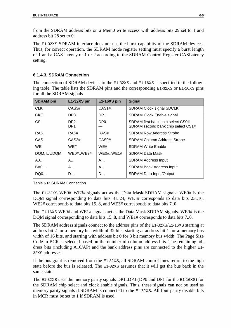
BUS INTERFACE 6-5
from the SDRAM address bits on a Mem0 write access with address bits 29 set to 1 andaddress bit 28 set to 0.
The E1-32XS SDRAM interface does not use the burst capability of the SDRAM devices.Thus, for correct operation, the SDRAM mode register setting must specify a burst lengthof 1 and a CAS latency of 1 or 2 according to the SDRAM Control Register CASLatencysetting.
6.1.4.3. SDRAM Connection
The connection of SDRAM devices to the E1-32XS and E1-16XS is specified in the follow-ing table. The table lists the SDRAM pins and the corresponding E1-32XS or E1-16XS pinsfor all the SDRAM signals.SDRAM pin E1-32XS pin E1-16XS pin Signal
CLK CAS3# CAS1# SDRAM Clock signal SDCLK
CKE DP3 DP1 SDRAM Clock Enable signal
CS DP2DP1
DP0—
SDRAM first bank chip select CS0#SDRAM second bank chip select CS1#
RAS RAS# RAS# SDRAM Row Address Strobe
CAS CAS2# CAS0# SDRAM Column Address Strobe
WE WE# WE# SDRAM Write Enable
DQM, L/UDQM WE0#..WE3# WE0#..WE1# SDRAM Data Mask
A0… A… A… SDRAM Address Input
BA0… A… A… SDRAM Bank Address Input
DQ0… D… D… SDRAM Data Input/Output
Table 6.6: SDRAM Connection
The E1-32XS WE0#..WE3# signals act as the Data Mask SDRAM signals. WE0# is theDQM signal corresponding to data bits 31..24, WE1# corresponds to data bits 23..16,WE2# corresponds to data bits 15..8, and WE3# corresponds to data bits 7..0.
The E1-16XS WE0# and WE1# signals act as the Data Mask SDRAM signals. WE0# is theDQM signal corresponding to data bits 15..8, and WE1# corresponds to data bits 7..0.
The SDRAM address signals connect to the address pins of the E1-32XS/E1-16XS starting ataddress bit 2 for a memory bus width of 32 bits, starting at address bit 1 for a memory buswidth of 16 bits, and starting with address bit 0 for 8 bit memory bus width. The Page SizeCode in BCR is selected based on the number of column address bits. The remaining ad-dress bits (including A10/AP) and the bank address pins are connected to the higher E1-32XS addresses.
If the bus grant is removed from the E1-32XS, all SDRAM control lines return to the highstate before the bus is released. The E1-32XS assumes that it will get the bus back in thesame state.
The E1-32XS uses the memory parity signals DP1..DP3 (DP0 and DP1 for the E1-16XS) forthe SDRAM chip select and clock enable signals. Thus, these signals can not be used asmemory parity signals if SDRAM is connected to the E1-32XS. All four parity disable bitsin MCR must be set to 1 if SDRAM is used.
6-6 CHAPTER 6
6.2. I/O Bus AccessHyperstone provides a completely separate I/O address range which makes it possible toconnect numerous peripheral devices each with individual behavior.
Bus timing and access mode for an I/O access is specified by bits 11..3 of the I/O address.
On an I/O access, the I/O read strobe IORD# or the I/O write strobe IOWR# is switchedlow for a read or write access respectively after the first access cycle, and it remains low forthe rest of the specified access cycles. The beginning of the IORD# or IOWR# signal canbe delayed by more than one cycle by specifying additional address setup cycles precedingthe access cycles. The beginning of the next bus access can be delayed by specifying bushold cycles succeeding the access cycles. Bus hold cycles are required by many I/O devicesdue to the time required to switch from driving the data bus to three-state.
Bit 11 of the I/O address enables a wait-pin controlled I/O access. The INT3/WAIT inputof the processor is sampled after the first three access cycles of the specified I/O accesstime. The I/O access will be extended by inserting further access cycles as long as the sig-nal at the WAIT input is asserted. When the WAIT signal becomes deasserted, the accesswill be terminated. Note that there is latency of about 2..3 processor cycles until a signalchange at the WAIT input becomes effective. The polarity of the WAIT signal can be pro-grammed via bit 26 of the Function Control Register FCR. When FCR(26) is set to 1 (de-fault after reset), the WAIT signal is high asserted; when FCR(26) is set to 0, the WAITsignal is low asserted. A minimum of four I/O access cycles must be specified when the I/Owait mode is being enabled.
When an I/O device requires R/W# direction and data strobe control, IORD# can be speci-fied (by address bit 10 = 1) as data strobe. WE# is then used as R/W# signal.
For normal I/O accesses, address bits 31..26 must be zero. Address bit 27 = 1 indicates aninternal I/O access of the processor. This is currently only used for the power-down andsleep modes (see Timer and CPU Clock Modes).

BUS INTERFACE 6-7
For I/O accesses, address setup, access and bus hold time can be specified by bits in the I/Oaddress as described in Figure 6.1. Reserved bits must always be supplied as zero whenspecifying an I/O address in a program.
0234578910
Reserved (must be 0)
Address Setup Time before Read or Write Access00 = 0 cycles01 = 2 cycles10 = 4 cycles11 = 6 cycles
Access Time for Read or Write Access000 = 2 cycles001 = 4 cycles010 = 6 cycles011 = 8 cycles100 = 10 cycles101 = 12 cycles110 = 14 cycles111 = 16 cycles
Bus Hold Time after Read or Write Access00 = 0 cycles01 = 2 cycles10 = 4 cycles11 = 6 cycles
Reserved for System Peripheral
11
Peripheral Device Control Mode0 = IORD# / IOWR# Strobe Control1 = R/W# / Data Strobe Control
2125
I/O Address and/or I/O Chip Select E1-16X: 6 BitsE1-32X: 10 Bits
1213
Wait Enable
Reserved for Internal Use (must be 0)
I/O Register Address
15
Figure 6.1: I/O Bus Control

6-8 CHAPTER 6
6.3. Bus Control Register BCRGlobal register G20 is the write-only bus control register BCR. The BCR defines the pa-rameters (bus timing, refresh control) for accessing external memory located in addressspaces MEM0..MEM3.
All bits of the BCR are set to one on Reset. They are intended to be initialized according tothe hardware environment.
Bits Name Description
31..28 Mem3Access Access time for address space MEM31111 = 16 clock cycles1110 = 15 clock cycles1101 = 14 clock cycles1100 = 13 clock cycles1011 = 12 clock cycles1010 = 11 clock cycles1001 = 10 clock cycles1000 = 9 clock cycles0111 = 8 clock cycles0110 = 7 clock cycles0101 = 6 clock cycles0100 = 5 clock cycles0011 = 4 clock cycles0010 = 3 clock cycles0001 = 2 clock cycles0000 = 1 clock cycle
27..24 Mem2Access Access time for address space MEM21111 = 16 clock cycles1110 = 15 clock cycles1101 = 14 clock cycles1100 = 13 clock cycles1011 = 12 clock cycles1010 = 11 clock cycles1001 = 10 clock cycles1000 = 9 clock cycles0111 = 8 clock cycles0110 = 7 clock cycles0101 = 6 clock cycles0100 = 5 clock cycles0011 = 4 clock cycles0010 = 3 clock cycles0001 = 2 clock cycles0000 = 1 clock cycle

BUS INTERFACE 6-9
6.3. Bus Control Register BCR (continued)Bits Name Description
23 Mem1Hold Bus hold time for address space MEM1When BCR(22) = 1:1 = 2 clock cycles0 = 1 clock cycle
When BCR(22) = 0:1 = 1 clock cycle0 = 0 clock cycles
22..20 Mem1Access Access time for address space MEM1111 = 8 clock cycles110 = 7 clock cycles101 = 6 clock cycles100 = 5 clock cycles011 = 4 clock cycles010 = 3 clock cycles001 = 2 clock cycles000 = 1 clock cycle
MEM0 = Non-DRAM (MCR(21) = 1):
19..16 Mem0Access Access time for address space MEM01111 = 16 clock cycles1110 = 15 clock cycles1101 = 14 clock cycles1100 = 13 clock cycles1011 = 12 clock cycles1010 = 11 clock cycles1001 = 10 clock cycles1000 = 9 clock cycles0111 = 8 clock cycles0110 = 7 clock cycles0101 = 6 clock cycles0100 = 5 clock cycles0011 = 4 clock cycles0010 = 3 clock cycles0001 = 2 clock cycles0000 = 1 clock cycle
15..14 Mem0Setup Address setup time for address space MEM011 = 3 clock cycles10 = 2 clock cycles01 = 1 clock cycle00 = 0 clock cycles
13..11 Mem0Hold Bus hold time for address space MEM0111 = 7 clock cycles110 = 6 clock cycles101 = 5 clock cycles100 = 4 clock cycles011 = 3 clock cycles010 = 2 clock cycles001 = 1 clock cycle000 = 0 clock cycles

6-10 CHAPTER 6
6.3. Bus Control Register BCR (continued)Bits Name Description
MEM0 = DRAM (MCR(21) = 0):
19..18 RasPrecharge RAS precharge time for address space MEM0 when MCR(8)=0 when MCR(8)=111 = 4 clock cycles 6 clock cycles10 = 3 clock cycles 5 clock cycles01 = 2 clock cycles 4 clock cycles00 = 1 clock cycle 3 clock cycles
17..16 CASAccess CAS access time for address space MEM0 when MCR(8)=0 when MCR(8)=111 = 4 clock cycles 6 clock cycles10 = 3 clock cycles 5 clock cycles01 = 2 clock cycles 4 clock cycles00 = 1 clock cycle 3 clock cycles
15..14 RasToCas RAS to CAS delay time11 = 4 clock cycles10 = 3 clock cycles01 = 2 clock cycles00 = 1 clock cycle
13..11 RefreshSelect Refresh rate select (CAS before RAS refresh)111 = Refresh disabled110 = Refresh every 4 prescaler time units101 = Refresh every 8 prescaler time units100 = Refresh every 16 prescaler time units011 = Refresh every 32 prescaler time units010 = Refresh every 64 prescaler time units001 = Refresh every 128 prescaler time units000 = Refresh every 256 prescaler time units
10..8 Mem3Hold Bus hold time for address space MEM3111 = 7 clock cycles110 = 6 clock cycles101 = 5 clock cycles100 = 4 clock cycles011 = 3 clock cycles010 = 2 clock cycles001 = 1 clock cycle000 = 0 clock cycles
7 Mem3Setup Address setup time for address space MEM31 = 1 clock cycle0 = 0 clock cycles
6..4 PageSizeCode Page size code

BUS INTERFACE 6-11
6.3. Bus Control Register BCR (continued)Bits Name Description
3 Mem2Setup Address setup time for address space MEM21 = 1 clock cycle0 = 0 clock cycles
2..0 Mem2Hold Bus hold time for address space MEM2111 = 7 clock cycles110 = 6 clock cycles101 = 5 clock cycles100 = 4 clock cycles011 = 3 clock cycles010 = 2 clock cycles001 = 1 clock cycle000 = 0 clock cycles
Table 6.7: Bus Control Register BCR
The DRAM type used and the physical page size of the DRAM are specified by bits 6..4 inthe BCR. Table 6.8 shows the encoding of BCR(6..4) and the associated column addressranges for memory areas with bus sizes of 32, 16 and 8 bits.
Column Address Range
BCR(6..4) 32-bit Bus Size 16-bit Bus Size 8-bit Bus Size
000 A15..A2 A15..A1 A15..A0
001 A14..A2 A14..A1 A14..A0
010 A13..A2 A13..A1 A13..A0
011 A12..A2 A12..A1 A12..A0
100 A11..A2 A11..A1 A11..A0
101 A10..A2 A10..A1 A10..A0
110 A9..A2 A9..A1 A9..A0
111 A8..A2 A8..A1 A8..A0
Table 6.8: Column Address Ranges

6-12 CHAPTER 6
6.4. Memory Control Register MCRGlobal register G27 is the write-only memory control register MCR. The MCR controlsadditional parameters for the external memory and the mapping of the entry table. All bitsof the MCR are set to one on Reset except for the MEM3BusSize bits that are initializedfrom the BOOTW and BOOTB pads. The MCR bits must be initialized according to thehardware environment and the desired function.
Bits Name Description
31 MEM3ParityDisable Parity check disable for address space MEM31 = disabled0 = enabled
30 MEM2ParityDisable Parity check disable for address space MEM21 = disabled0 = enabled
29 MEM1ParityDisable Parity check disable for address space MEM11 = disabled0 = enabled
28 MEM0ParityDisable Parity check disable for address space MEM01 = disabled0 = enabled
27 reserved
26 MEM2WaitDisable Wait signal disable for address space MEM21 = disabled0 = enabled
25..24 reserved
23 MEM2ByteMode Byte write access mode for address space MEM21 = WE0# .. WE3# act as byte write strobe0 = WE0# .. WE3# act as byte enable signal
MEM0 = Non-DRAM (MCR(21) = 1):
22 reserved
MEM0 = DRAM (MCR(21) = 0):
22 DRAMType2 1 = Mem0 DRAM type is according to MCR(15)0 = Mem0 DRAM type is SDRAM
21 MEM0MemoryType 1 = Non-DRAM0 = DRAM
20 reserved
19 MEM1ByteMode Byte write access mode for address space MEM11 = WE0# .. WE3# act as byte write strobe0 = WE0# .. WE3# act as byte enable signal
18..16 reserved
BUS INTERFACE 6-13
6.4. Memory Control Register MCR (continued)
Bits Name Description
MEM0 = Non-DRAM (MCR(21) = 1):
15 MEM0ByteMode Byte write access mode for address space MEM01 = WE0# .. WE3# act as byte write strobe0 = WE0# .. WE3# act as byte enable signal
MEM0 = DRAM (MCR(21) = 0):
15 DRAMType 1 = Fast Page Mode DRAMs0 = EDO DRAMs
14..12 EntryTableMap 111 = MEM3110 = reserved101 = reserved100 = reserved011 = Internal RAM (IRAM)010 = MEM2001 = MEM1000 = MEM0
11 MEM3BusHoldBreak 1 = Break Disabled0 = Break Enabled
10 MEM2BusHoldBreak 1 = Break Disabled0 = Break Enabled
9 MEM1BusHoldBreak 1 = Break Disabled0 = Break Enabled
MEM0 = Non-DRAM (MCR(21) = 1):
8 MEM0BusHoldBreak 1 = Break Disabled0 = Break Enabled
MEM0 = DRAM (MCR(21) = 0):
8 DRAMBusHold 1 = Break Enabled, Bus Hold time 1 cycle0 = Break Enabled, Bus Hold time 0 cycles

6-14 CHAPTER 6
6.4. Memory Control Register MCR (continued)
Bits Name Description
7..6 MEM3BusSize 11 = 8 bit10 = 16 bit01 = reserved00 = 32 bit
5..4 MEM2BusSize 11 = 8 bit10 = 16 bit01 = reserved00 = 32 bit
3..2 MEM1BusSize 11 = 8 bit10 = 16 bit01 = reserved00 = 32 bit
1..0 MEM0BusSize 11 = 8 bit10 = 16 bit01 = reserved00 = 32 bit
Table 6.9: Memory Control Register MCR
6.4.1. MEMx Parity DisableBits 31..28 of the MCR control parity generation and parity check for each memory area.The default setting is parity check disabled. The appropriate MCR bit must be cleared toenable the parity check for that memory area.
Since the SDRAM interface uses the data parity signals as SDRAM control signals, theMEMxParityDisable bits must all be set to 1 when the SDRAM interface is used.
6.4.2. MEM2 Wait DisableBit 26 of the MCR controls the wait pin function for the memory area MEM2. The defaultsetting is wait function disabled. The MCR bit must be cleared to enable the wait functionfor the MEM2 memory area. When this function is enabled, the INT3/WAIT input of theprocessor is used as wait pin. Any MEM2 memory access remains active as long as thesignal at the WAIT input is asserted (the WAIT input is sampled after the first three accesscycles of the memory access). The access will be terminated after the WAIT input becomesdeasserted. Whether the input is low-asserted or high-asserted can be programmed via bit26 of the Function Control Register FCR. A minimum access time of four cycles must bespecified for a memory area with the wait function enabled.
If the INT3/WAIT input is used as wait pin, bit 30 of the FCR (INT3Mask) should be set to1 so that no interrupts are generated on the assertion of WAIT.
6.4.3. MEMx Byte ModeBit 23, 19, and 15 of the MCR control the byte write access mode for memory areasMEM2, MEM1, and MEM0, respectively. The default setting is byte-write-strobe, meaningthat the signals WE0#..WE3# are used as write strobe signals for writing the appropriate

BUS INTERFACE 6-15
data byte to the external memory. When the MCR bit is cleared, the signals WE0#..WE3#act as a byte enable signal and the general WE# signal must be used for writing the data tothe memory.
Note: Most SRAM chips with 16-bit or 32-bit wide data interface require a single write-enable signal and dedicated enable signals for each byte. The setting MEMxByteMode = 0is intended specifically for those types of memories.
6.4.4. DRAMType and DRAMType2When the MEM0 memory type is set to DRAM (MCR(21) = 0), bits 15 and 22 of the MCRact as control bits for selecting the DRAM type as specified in the following table. Thedefault setting is Fast Page Mode DRAM.
MCR(22) MCR(15) DRAM Type
1 1 Fast Page Mode
1 0 EDO
0 1 SDRAM
0 0 reserved
Table 6.9: DRAM Type Selection
When the DRAM type indicates Fast-Page-Mode DRAMs, the OE# signal of the processoris left deasserted during DRAM accesses. The OE# pin of the DRAMs must then be tiedlow for correct DRAM operation.
When the DRAM type indicates EDO DRAMs, OE# must be connected to the DRAMsand is asserted on DRAM read accesses. OE# stays active for one half clock cycle past theend of the CAS# signals, the read data is sampled at the end of OE#. Thus, the processorcan take advantage of the EDO feature.
When the DRAM type indicates SDRAM, SDRAM accesses are enabled through theSDRAM Control Register SDCR. Since the SDRAM interface uses the data parity signalsas SDRAM control signals, the MEMxParityDisable bits must all be set to 1 when theSDRAM interface is used.
6.4.5. Entry Table MapBits 14..12 of the MCR map the entry table to one of the memory areas MEM0..MEM3 orto the IRAM. With a mapping to MEM3 (default setting), the entry table is mapped to theend of MEM3, with all other settings, the entry table is mapped to the beginning of thespecified memory area.
6.4.6. MEMx Bus Hold BreakBits 11..8 specify a memory bus hold break for MEM3..MEM0 respectively. The defaultsetting is disabled. With enabled, bus hold cycles are skipped when the next memory accessaddresses the same memory area. Regularly, the bus hold break should be enabled; it mustonly be left disabled to accommodate (rare) SRAMs or ROMs which need all specified cy-cles before a new access can be started (e.g. for charge restore).
6-16 CHAPTER 6
If the MEM0 memory type is DRAM, MCR bit 8 changes the RasPrecharge and CASAc-cess cycle counts specified in BCR, and specifies a bus hold time of 0 or 1 cycles. Bus holdbreak for DRAM is always enabled.
6.4.7. MEMx Bus SizeBits 7..0 specify the bus size for each of the four memory areas.
BUS INTERFACE 6-17
6.5. SDRAM Control Register SDCRThe SDRAM Control Register SDCR specifies the SDRAM access parameters. This reg-ister must be set before the first SDRAM access (SDRAM mode register set) is performed.All bits of this register are initialized to 1 on reset. The SDCR is set from the address bitsof a Mem0 write access with address bits 29 and 28 set to 1 (see section 6.1.4 SDRAM BusAccess).
Bits Name Description
31..28 Must be 0011
27..21 Reserved, must be 0
20..12 BankAddrEnable Enable bits for Bank Address bits 28..201 = corresponding address bit is a bank address bit0 = corresponding address bit is not a bank address bit
11 CS1Enable Enable for second SDRAM chip select output1 = second SDRAM chip select CS1# is disabled0 = second SDRAM chip select CS1# is enabled
10..8 CS1Select Code for selection between SDRAM chip selects CS0# and CS1#111 = address bit 28 selects between CS0# and CS1#110 = address bit 27 selects between CS0# and CS1#…000 = address bit 21 selects between CS0# and CS1#If the corresponding address bit is 0, CS0# is activated, if theaddress bit is 1, CS1# is activated.
7 Reserved, must be 1
6 CASLatency 1 = CAS Latency 2 clock cycles0 = CAS Latency 1 clock cycle
5..4 Reserved, must be 1
3 SDCLKSelect SDCLK Clock Rate Select1 = SDCLK is CPU clock / 20 = SDCLK is CPU clock
2 Reserved, must be 0
1..0 Must be 00
6.5.1. BankAddrEnableThe BankAddrEnable parameter specifies which of the CPU address bits 28..20 areSDRAM bank address bits. For SDRAM devices with two memory banks, only one ofthese bits should be set. For SDRAM devices with four memory banks, two of these bitsshould be set. If the second SDRAM Chip Select is used, the corresponding BankAddrEn-able bit must also be set.
The E1-32XS supports holding two different SDRAM banks active.
6.5.2. CS1EnableNormally, a single SDRAM chip select signal CS0# is generated. In systems with a second(identical) bank of SDRAM devices, setting CS1Enable to 0 enables the generation of thechip select signal CS1# for this second bank of SDRAM devices. This feature is not sup-ported on the E1-16XS, the CS1Enable bit must be set to 1 in this case.

6-18 CHAPTER 6
6.5.3. CS1SelectOn systems with two banks of identical SDRAM devices, the CS1Select bits specify whichaddress bit should be used to discriminate between the chip select signals CS0# and CS1#.The bit corresponding the CS1Select address line must also be set in the BankAddrEnablefield.
6.5.4. CASLatencyThe CASLatency bit specifies the CAS latency of the SDRAM devices. This bit must re-flect the CAS latency setting in the SDRAM Mode Register.
6.5.5. SDCLKSelectThe SDCLKSelect bit specifies the SDRAM clock signal rate. The SDCLK signal can beselected to run at the full CPU clock rate or at half the CPU clock rate. For a CPU clock ofmore than 40 MHz, the SDRAM clock rate must be set to half the CPU clock rate.
The CAS access time in BCR must be set according to the SDCLKSelect bit in SDCR. IfSDCLK is the CPU clock, the CAS access time must be set to 1 clock cycle, if SDCLK isCPU clock / 2, the CAS access time must be set to 2 clock cycles.
The RAS precharge time and RAS-to-CAS delay time settings in BCR must be set to amultiple of two (2, 4 or 6) if SDCLK is CPU clock / 2. The RAS precharge setting controlsthe time for the SDRAM precharge command, the RAS-to-CAS delay setting controls thetime for the SDRAM row activate command.
6.5.6. SDRAM Connection ExampleOne 64 Mbit SDRAM device (4 banks × 1M × 16 bits) is connected to the E1-16XS to forma 16 bit wide 8 Mbyte SDRAM memory space. Column addresses are SDRAM pins A0 toA7, row address pins are SDRAM pins A0 to A11. There are two bank address pins BA0and BA1.
Since the memory system is 16 bit wide, the SDRAM is connected to the E1-16XS startingwith E1-16XS address pin 1. There are 8 column addresses, so the page size code is 7.
The SDRAM address pins A0..A7 carry E1-16XS address bits 1..8 on a column access, andE1-16XS address bits 9..16 on a row access. SDRAM pins A8, A9, A10/AP and A11 mustbe connected to E1-16XS address bits 17..20. These are available on E1-16XS address pinsA10 to A13. The bank address pins BA0 and BA1 are connected to E1-16XS address bits 21and 22 on pins A14 and A15.
The data bus connects E1-16XS D0..D15 to DQ0..DQ15, LDQM connects to WE1#, andUDQM to WE0#.
The SDCR settings are thus:BankAddrEnable 000000110 bank address bits 21, 22CS1Enable 1 CS1# signal disabledCS1Select 111 - unused

BUS INTERFACE 6-19
6.6. Input Status Register ISRGlobal register G25 is the read-only input status register ISR. The ISR reflects the inputlevels at the pins IO1..IO3 as well as the input levels at the four interrupt pins INT1..INT4and contains the EventFlag, the EqualFlag, the WatchdogFlag and the ClockOnFlag. Re-served bits are read as zeros.
The input levels are not affected by the polarity bits in the Function Control Register FCR,they reflect always the true signal level at the corresponding pins with a latency of 2..3 cy-cles, a 1 signals high level.
Bits Name Description
31..11 reserved
10 ClockOnFlag Determines the source of the last reset event1 = Last reset caused by sleep mode wakeup0 = Last reset caused by RESET# signal or watchdog timer
9 WatchdogFlag Determines the source of the last reset event1 = Last reset caused by watchdog timer (IO3 timer)0 = Last reset caused by RESET# signal or sleep mode wakeup
8 EventFlag Set to 1 in IO3Timing Mode when IO3Level is equal to IO3PolarityCleared to 0 by FCR(13) = 1 or write to the WCR
7 EqualFlag Set to 1 in IO3Timing Mode or IO3TimerInterrupt Mode whenWCR(15..0) = TR(15..0)Cleared to 0 by FCR(13) = 1 or write to the WCR
6 IO3Level Reflects the signal level at the IO3 Pin1 = High Level0 = Low Level
5 IO2Level Reflects the signal level at the IO2 Pin1 = High Level0 = Low Level
4 IO1Level Reflects the signal level at the IO1 Pin1 = High Level0 = Low Level
3 INT4Level Reflects the signal level of interrupt input INT41 = High Level0 = Low Level
2 INT3Level Reflects the signal level of interrupt input INT31 = High Level0 = Low Level
1 INT2Level Reflects the signal level of interrupt input INT21 = High Level0 = Low Level
0 INT1Level Reflects the signal level of interrupt input INT11 = High Level0 = Low Level
Table 6.10: Input Status Register ISR

6-20 CHAPTER 6
6.7. Function Control Register FCRGlobal register G26 is the write-only function control register FCR. The FCR controls thepolarity and function of the I/O pins IO1..IO3 and the interrupt pins INT1..INT4, the timerinterrupt mask and priority, the bus lock, the CLKOUT pin and the Extended Overflowexception. All bits of the FCR are set to one on a Reset exception (from the RESET# pin oras a result of a watchdog overrun). They must be initialized according to the hardware en-vironment and the desired function. The reserved bits must not be changed when the FCRis updated. The FCR is preserved on a clock-down reset in order to have the correct inter-rupt mask and polarity for the wakeup from clock-down.
Each of the four interrupt pins INT1..INT4 can cause a processor interrupt when the corre-sponding interrupt mask bit is cleared. The corresponding polarity bit determines whetherthe signal at the interrupt pin must be low (polarity bit = 0) or high (polarity bit = 1) tocause an interrupt. Additionally, the internal timer interrupt can be enabled or disabledseparately.
Each of the I/O pins IO1..IO3 can be either used as input or interrupt signal (IOxDirection= 1) or as output (IOxDirection = 0). The CLKOUT pin of the processor can be pro-grammed to provide a static output level of either high or low, or it can be configured toprovide the processor's internal clock signal divided by a programmable factor.
Bits Name Description
31 INT4Mask 1 = Interrupt INT4 Disabled0 = Interrupt INT4 Enabled
30 INT3Mask 1 = Interrupt INT3 Disabled0 = Interrupt INT3 Enabled
29 INT2Mask 1 = Interrupt INT2 Disabled0 = Interrupt INT2 Enabled
28 INT1Mask 1 = Interrupt INT1 Disabled0 = Interrupt INT1 Enabled
27 INT4Polarity 1 = Non-Inverted (Interrupt on High Level)0 = Inverted (Interrupt on Low Level)
26 INT3Polarity 1 = Non-Inverted (Interrupt on High Level)0 = Inverted (Interrupt on Low Level)
25 INT2Polarity 1 = Non-Inverted (Interrupt on High Level)0 = Inverted (Interrupt on Low Level)
24 INT1Polarity 1 = Non-Inverted (Interrupt on High Level)0 = Inverted (Interrupt on Low Level)
23 TINTDisable 1 = Timer Interrupt Disabled0 = Timer Interrupt Enabled
22 CLKOUTPolarity 1 = Inverted / High0 = Non-Inverted / Low
21..20 TimerPriority 11 = Priority 6 (higher than Priority of INT1)10 = Priority 8 (higher than Priority of INT2)01 = Priority 10 (higher than Priority of INT3)00 = Priority 12 (higher than Priority of INT4)
19..18 CLKOUTControl CLKOUT pin control

BUS INTERFACE 6-21
6.7. Function Control Register FCR (continued)Bits Name Description
17 BusLock DMA Access:1 = Non-Locked0 = Locked out
16 EOVDisable Extended Overflow Exception:1 = Disabled0 = Enabled
15..14 reserved
13..12 IO3Control IO3 Control State:11 = IO3Standard Mode10 = Watchdog Mode01 = IO3Timing Mode00 = IO3TimerInterrupt Mode
11 CLKOUTControl2 CLKOUT pin control
10 IO3Direction 1 = Input0 = Output
9 IO3Polarity 1 = Non-Inverted0 = Inverted
8 IO3Mask On Input:1 = IO3 Interrupt Disabled0 = IO3 Interrupt EnabledOn Output:1 = IO3 Output reflects IO3Polarity0 = Reserved
7 reserved
6 IO2Direction 1 = Input0 = Output
5 IO2Polarity 1 = Non-Inverted0 = Inverted
4 IO2Mask On Input:1 = IO2 Interrupt Disabled0 = IO2 Interrupt EnabledOn Output:1 = IO2 Output reflects IO2Polarity0 = Reserved
3 reserved
2 IO1Direction 1 = Input0 = Output
1 IO1Polarity 1 = Non-Inverted0 = Inverted
0 IO1Mask On Input:1 = IO1 Interrupt Disabled0 = IO1 Interrupt EnabledOn Output:1 = IO1 Output reflects IO1Polarity0 = Reserved
Table 6.11: Function Control Register FCR

6-22 CHAPTER 6
6.7.1. CLKOUTControl and CLKOUTControl2The CLKOUTControl and CLKOUTControl2 fields control the function of the CLKOUTpin according to the following table:
FCR(11) FCR(19) FCR(18) CLKOUT function
1 1 1 Output reflects CLKOUTPolarity
1 1 0 Processor clock
1 0 1 Processor clock / 2
1 0 0 Processor clock / 4
0 1 1 Processor clock / 6
0 1 0 Processor clock / 8
0 0 1 Processor clock / 12
0 0 0 Processor clock / 16
6.8. Watchdog Compare Register WCRGlobal register G24 is the watchdog compare register WCR. Only bits 15..0 are used, bits31..16 are reserved, they must be zero on a move to the WCR. In the present version, bits31..16 are read as zero. The WCR is used by the IO3 control modes (see section 6.9. IO3Control Modes).
6.9. IO3 Control ModesAdditionally to the standard use like IO1 and IO2 (see section 6.10.3. Bus Signal Descrip-tion), there are special control modes in combination with the IO3 pin. These controlmodes are specified by FCR(13) and FCR(12).
On all IO3 control modes, the watchdog compare register WCR must be set before thecontrol mode is specified in the FCR, otherwise the EqualFlag could be set erroneously.
The EqualFlag and the EventFlag are being cleared on all IO3 control modes by either set-ting FCR(13) to one or a move to the watchdog compare register WCR.
6.9.1. IO3Standard ModeFCR(13) = 1, FCR(12) = 1 specifies IO3Standard mode.
Standard use of IO3 without any additional IO3 control functions. See section 6.10.3. forsignals IO1..IO3.
6.9.2. Watchdog ModeFCR(13) = 1, FCR(12) = 0 specifies Watchdog mode.
A Reset exception occurs when WCR(15..0) = TR(15..0). The standard use of IO3 is notaffected.
6.9.3. IO3Timing ModeFCR(13) = 0, FCR(12) = 1 specifies the IO3Timing mode.

BUS INTERFACE 6-23
On IO3Direction = Input:
When input signal IO3Level = IO3Polarity, the EventFlag ISR(8) is set and the currentcontents of the TR(15..0) is copied to the WCR. Thus, the time of the event indicated bythe 16 low-order bits of the TR is captured in the WCR. When WCR(15..0) = TR(15..0)before the EventFlag is set, the EqualFlag ISR(7) is set. Either flag set causes an interruptwhen the IO3 interrupt is enabled.
Note: The EventFlag and the EqualFlag can be used to distinguish between an input signaltransition and a time-out. The EventFlag can be set even after the EqualFlag (but not viceversa) during the interrupt latency time; thus, when the EventFlag is set, WCR(15..0) con-tains always the time when the input reached the level specified by IO3Polarity. Note thatthe EventFlag is immediately set on entering IO3Timing mode when the input signal isalready on the specified level. WCR(15..0) must be set to a value different from the valueof the TR(15..0), otherwise the EqualFlag is set immediately. The maximum span for thetime-out is 216-1 ticks of the TR.
IO3Direction = Output:
When WCR(15..0) = TR(15..0), the EqualFlag is set and an interrupt occurs when the IO3interrupt is enabled. Additionally, an internal toggle latch is toggled. The IO3 output signalis high when the value of the toggle latch and IO3Polarity are not equal, otherwise low.Thus, each toggling causes a transition of the IO3 output signal. The toggle latch is clearedby setting FCR(13) to 1.
Note: This mode can be used to create an arbitrary output signal sequence by just updatingthe WCR. When the program switches to IO3Standard mode after the end of a signal se-quence and the toggle latch remained set to 1, FCR(13) must be set to 1 and IO3Polarity beinverted coincidentally in the same move to FCR to avoid a transition of the IO3 outputsignal. The IO3 interrupt must also be disabled in the same move to FCR to avoid an inter-rupt from the output signal.
6.9.4. IO3TimerInterrupt ModeFCR(13) = 0, FCR(12) = 0 specifies the IO3TimerInterrupt mode.
Additionally to the standard use of IO3, the condition WCR(15..0) = TR(15..0) sets theEqualFlag ISR(7) and causes an IO3 interrupt regardless of the IO3Mask in FCR(8).
Note: When the IO3 interrupt is disabled, the IO3TimerInterrupt mode can be used inde-pendently of the use of IO3 as input or output. When the IO3 interrupt is enabled, theIO3TimerInterrupt mode can be used as a time-out for the IO3 interrupt. The EqualFlag canthen be used to distinguish between time-out and an IO3 interrupt.
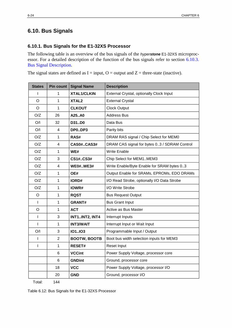
6-24 CHAPTER 6
6.10. Bus Signals
6.10.1. Bus Signals for the E1-32XS ProcessorThe following table is an overview of the bus signals of the hyperstone E1-32XS microproc-essor. For a detailed description of the function of the bus signals refer to section 6.10.3.Bus Signal Description.
The signal states are defined as I = input, O = output and Z = three-state (inactive).
States Pin count Signal Name Description
I 1 XTAL1/CLKIN External Crystal, optionally Clock Input
O 1 XTAL2 External Crystal
O 1 CLKOUT Clock Output
O/Z 26 A25..A0 Address Bus
O/I 32 D31..D0 Data Bus
O/I 4 DP0..DP3 Parity bits
O/Z 1 RAS# DRAM RAS signal / Chip Select for MEM0
O/Z 4 CAS0#..CAS3# DRAM CAS signal for bytes 0..3 / SDRAM Control
O/Z 1 WE# Write Enable
O/Z 3 CS1#..CS3# Chip Select for MEM1..MEM3
O/Z 4 WE0#..WE3# Write Enable/Byte Enable for SRAM bytes 0..3
O/Z 1 OE# Output Enable for SRAMs, EPROMs, EDO DRAMs
O/Z 1 IORD# I/O Read Strobe, optionally I/O Data Strobe
O/Z 1 IOWR# I/O Write Strobe
O 1 RQST Bus Request Output
I 1 GRANT# Bus Grant Input
O 1 ACT Active as Bus Master
I 3 INT1..INT2, INT4 Interrupt Inputs
I 1 INT3/WAIT Interrupt Input or Wait Input
O/I 3 IO1..IO3 Programmable Input / Output
I 2 BOOTW, BOOTB Boot bus width selection inputs for MEM3
I 1 RESET# Reset Input
6 VCCint Power Supply Voltage, processor core
6 GNDint Ground, processor core
18 VCC Power Supply Voltage, processor I/O
20 GND Ground, processor I/O
Total: 144
Table 6.12: Bus Signals for the E1-32XS Processor

BUS INTERFACE 6-25
6.10.2. Bus Signals for the E1-16XS ProcessorThe following table is an overview of the bus signals of the hyperstone E1-16XS microproc-essor. For detailed description of the function of the bus signals refer to section 6.10.3. BusSignal Description.
The signal states are defined as I = input, O = output and Z = three-state (inactive).
States Pin count Signal-Names Description
I 1 XTAL1/CLKIN External Crystal, optionally Clock Input
O 1 XTAL2 External Crystal
O 1 CLKOUT Clock Output
O/Z 22 A21..A0 Address Bus
O/I 16 D15..D0 Data Bus
O/I 2 DP0..DP1 Parity bits
O/Z 1 RAS# DRAM RAS signal / Chip Select for MEM0
O/Z 2 CAS0#..CAS1# DRAM CAS signal for bytes 0..1 / 2..3 / SDRAM Control
O/Z 1 WE# Write Enable
O/Z 3 CS1#..CS3# Chip Select for MEM1..MEM3
O/Z 2 WE0#..WE1# Write Enable/Byte Enable for SRAM bytes 0..1 / 2..3
O/Z 1 OE# Output Enable for SRAMs, EPROMs, EDO DRAMs
O/Z 1 IORD# I/O Read Strobe, optionally I/O Data Strobe
O/Z 1 IOWR# I/O Write Strobe
O 1 RQST Bus Request Output
I 1 GRANT# Bus Grant Input
O 1 ACT Active as Bus Master
I 3 INT1..INT2, INT4 Interrupt Inputs
I 1 INT3/WAIT Interrupt Input or Wait Input
O/I 3 IO1..IO3 Programmable Input / Output
I 1 BOOTB Boot bus width selection input for MEM3
I 1 RESET# Reset Input
6 VCCint Power Supply Voltage, processor core
6 GNDint Ground, processor core
9 VCC Power Supply Voltage, processor I/O
12 GND Ground, processor I/O
Total: 100
Table 6.13: Bus Signals for the E1-16XS Processor
6-26 CHAPTER 6
6.10.3. Bus Signal DescriptionThe following section describes the bus signals for both the hyperstone E1-32XS and E1-16XS microprocessor in detail.
In the following signal description, the signal states are defined as I = input, O = output andZ = three-state (inactive).
States Names Use
I XTAL1/CLKIN Input for quartz crystal. When the clock is generated by an ex-ternal clock generator, XTAL1 is used as clock input. The clocksignal is multiplied by eight and divided according to the TPRsetting to generate the internal clock.
O XTAL2 Output for quartz crystal. XTAL2 is not connected when an ex-ternal clock generator is used.
O CLKOUT Clock signal output or programmable output. CLKOUT can beselected as a programmable output pin or as output deliveringthe CPU clock signal divided by factors from 1 to 16. CLKOUTcan be used to supply a clock signal to peripheral devices.
O/Z A25..A0 The address bits A25..A0 represent the address bus. An activehigh bit signals a "one". A0 is the least significant bit. With theE1-16X, only A21..A0 are connected to the address bus pins.
O/I D31..D0 Data bus. The signals D31..D0 (D15..D0 with the E1-16XS) rep-resent the bi-directional data bus; active high signals a "one".At a read access, data is transferred from the data bus to the reg-ister set or to the instruction cache only at the cycle corre-sponding to the last actual read access cycle, thus inhibiting gar-bled data from being transferred.At a write access, the data bus signals are activated during theaddress setup, write and bus hold cycle(s).A half-word or byte to be written is multiplexed from its right-adjusted position in a register to the addressed half-word or byteposition. Thus, no external multiplexing of data signals is re-quired.On a 32-bit wide memory area, byte addresses 0, 1, 2 and 3 cor-respond to D31..D24, D23..D16, D15..D8 and D7..D0 respec-tively.On a 16-bit wide memory area, byte address 2 and 3 in the firstaccess and byte addresses 0 and 1 in the second access corre-spond to D15..D8 and D7..D0 respectively.On a 8-bit wide memory area, byte addresses 3..0 correspond toD7..D0 in succeeding accesses.

BUS INTERFACE 6-27
6.10.3. Bus Signal Description (continued)States Names Use
O/I DP0..DP3 Data Parity signals if SDRAM interface is not used. DP0..DP3represent the bi-directional parity signals; active high indicates a"one". With the E1-32XS, DP0, DP1, DP2 and DP3 correspondto D31..D24, D23..D16, D15..D8 and D7..D0 respectively. Withthe E1-16XS, DP0 and DP1 correspond to D15..D8 and D7..D0respectively.At a write access, all data parity signals are activated during theaddress setup, write and bus hold cycles.At a read access, the corresponding data parity signals are evalu-ated at the last read access cycle when parity checking for theaddressed memory area is enabled.Parity "odd" is used, that is, the correct parity bit is "one" whenall bits of the corresponding byte are "zero".
If the SDRAM interface is used, the parity signals are not avail-able, and the DP pins are redefined as SDRAM control signals.DP3 (DP1 for the E1-16XS) acts as the SDRAM CKE (clock en-able) signal. A pull-up resistor should be connected to this sig-nal.DP2 (DP0 for the E1-16XS) acts as the SDRAM Chip Select sig-nal for SDRAM bank 0. DP1 acts as the SDRAM Chip Selectsignal for SDRAM bank 1 (not available for the E1-16XS).DP0 is not used on the E1-32XS when the SDRAM interface isselected.
O/Z RAS# Row Address Strobe. Active low indicates row address strobeasserted.RAS# is activated high and then again low when the processoraccesses a new page in the DRAM address space, that is whenany of the (high order) RAS address bits is different from theRAS address bits of the last DRAM access. RAS# is left lowafter any own DRAM access.RAS# is activated high, low and then high by a refresh cycle.After the bus has been regained from another bus master, theprocessor starts the next DRAM access as a RAS access.At any non-RAS address cycle, RAS# is left unchanged, thus, apreviously selected DRAM page is not affected.When the SDRAM interface is used, this signal provides theSDRAM RAS signal.When non-DRAM memory is placed in memory area MEM0,RAS# is used as the chip select signal for this memory.

6-28 CHAPTER 6
6.10.3. Bus Signal Description (continued)States Names Use
O/Z CAS0#..CAS3# Column Address Strobe for Fast Page or EDO DRAM. Activelow indicates column address strobe asserted. CAS0#..CAS3#are only used by a DRAM for column access cycles and for"CAS before RAS" refresh.With the E1-32XS, CAS0#..CAS3# correspond to the column ad-dress enable signals for D31..D24, D23..D16, D15..D8 andD7..D0 respectively.With the E1-16XS, CAS0# and CAS1# correspond to the columnaddress enable signals for D15..D8 and D7..D0 respectively.
If the SDRAM interface is used, these signals are redefined asSDRAM control signals.CAS3# (CAS1# for the E1-16XS) provides the SDRAM clocksignal.CAS2# (CAS0# for the E1-16XS) provides the SDRAM CASsignal.CAS0# and CAS1# are not used on the E1-32XS when theSDRAM interface is selected.
O/Z WE# Write Enable. WE# is signaled in the same cycle(s) as the ad-dress signals. Active low indicates a write access, active highindicates a read access.WE# is intended to be used as DRAM Write Enable and asR/W# for I/O access when IORD# is specified as data strobe(see IORD#). WE# is also used as SRAM Write Enable whenthe WE0#..WE3# signals are used as byte enable signals.Note: WE# can also be used to control bus transceivers when pe-ripheral devices or slow memories must be separated from theprocessor data bus in order to decrease the capacitive load of theprocessor data bus.
O/Z CS1#..CS3# Chip Select. Chip select is signaled in the same cycle(s) as theaddress signals. Active low of CS1#..CS3# indicates chip selectfor the memory areas MEM1..MEM3 respectively.Note: RAS# is used as chip select for a non-DRAM memory inMEM0.
O/Z WE0#/BE0# SRAM Write Enable. Active low indicates write enable for the..WE3#/BE3# corresponding byte, active high indicates write disable.
When the byte mode for the corresponding memory area is en-abled, WE0#..WE3# are used as byte enables BE0#..BE3#; lowindicates enable, high indicates disable. The WE# signal is thenused as write enable signal.If the SDRAM interface is used, these signals provide the DQMsignals for the SDRAM memory.With the E1-32XS, WE0#..WE3# correspond to the enable sig-nals for D31..D24, D23..D16, D15..D8 and D7..D0 respectively.With the E1-16XS, WE0# and WE1# correspond to the enablesignals for D15..D8 and D7..D0 respectively.
BUS INTERFACE 6-29
6.10.3. Bus Signal Description (continued)States Names Use
O/Z OE# Output Enable for SRAM, EPROM, EDO DRAM, andSDRAM. OE# is active low on a SRAM, EPROM or DRAM(except Fast Page Mode) read access.
O/Z IORD# I/O Read Strobe, optionally I/O data strobe. The use of IORD# isspecified in the I/O address. Address bit 10 = 0 specifies I/Oread strobe, address bit 10 = 1 specifies I/O data strobe. Whenspecified as I/O read strobe, IORD# is low on I/O read accesscycles, high on all other cycles. When specified as I/O datastrobe, IORD# is low on any I/O access cycles, high on all othercycles.Note: When IORD# is specified as I/O data strobe, WE# can beused as R/W# signal.
O/Z IOWR# I/O Write Strobe. When specified as I/O write strobe by I/O ad-dress bit 10 = 0, IOWR# is active low on I/O write access cycles.
O RQST RQST signals the bus request for a memory or I/O access. RQSTis high from the beginning of the request until the requested ac-cess is completed.
I GRANT# Bus Grant. GRANT# is signaled low by an (off-chip) bus arbiterto grant access to the bus for memory and I/O cycles. WhenGRANT# is switched from low to high during an access, the busis only released to another bus master after completion of thecurrent access. The GRANT# signal supplied by a bus arbitermay be asynchronous to the clock; it is synchronized on-chip toavoid metastability. For systems with a single bus master,GRANT# must be tied low.Note: GRANT# is recommended to be kept low by the bus ar-biter on the bus master with the last access; thus, any subsequentaccess by the same bus master saves the synchronization time.
O ACT Active as bus master. ACT is signaled high when GRANT# islow and it is kept high during a current bus access. SinceGRANT# is asynchronous, ACT follows GRANT# with a delayof 2..3 cycles. ACT is also kept high on a bus lock (FCR(17) = 0) from the beginning of the first access after FCR(17) iscleared to zero until the bus lock is released by setting FCR(17)to one.Note: When ACT transits from high to low, the address and databus are switched to threestate (inactive). All bus control signalsmarked O/Z are driven high and then switched to threestate.These signals are kept high by an on-chip resistor (ca. 1 MΩ)tied on-chip to Vcc.

6-30 CHAPTER 6
6.10.3. Bus Signal Description (continued)States Names Use
I INT1..INT4 Interrupt Request. A signal of a specified level on any of theINT1..INT4 interrupt request pins causes an interrupt exceptionwhen the interrupt lock flag L is zero and the correspondingINTxMask bit in FCR is not set. The INTxPolarity bits in FCRspecify the level of the INTx signals: INTxPolarity = 1 causes aninterrupt on a high input signal level, INTxPolarity = 0 causes aninterrupt on a low input signal level. INT1..INT4 may be sig-naled asynchronously to the clock; they are not stored internally.A transition of INT1..INT4 is effective after a minimum of threecycles. The response time may be much higher depending on thenumber of cycles to the end of the current instruction or thenumber of cycles until the interrupt lock flag L is cleared.The signal on the INT3 input can also be used as WAIT signalwhen the wait controlled memory or I/O access mode is enabled.Note: The signal level of INT1..INT4 can be inspected inISR(0)..ISR(3). Thus, with the corresponding INTxMask bit set,INT1..INT4 can be used just as input signals.
O/I IO1..IO3 General Input-Output. IO1..IO3 can be individually configuredvia IOxDirection bits in the FCR as either input or output pins.When configured as input, IO1..IO3 can be used likeINT1..INT4 for additional interrupt or input signals.When configured as output, the IOxPolarity bit in FCR specifiesthe output signal level. IOxPolarity = 1 specifies a high level,IOxPolarity = 0 specifies a low level. IO1..IO3 are alwaysswitched rail-to-rail regardless of the setting of MCR(25). Anoutput signal at IO1 or IO2 cannot cause an interrupt regardlessof the corresponding IOxMask bit; however, it can be inspectedas IOxLevel in ISR (e.g. for testing). IO3 can be used for variouscontrol functions.
I RESET# Reset processor. RESET# low resets the processor to the initialstate and halts all activity. RESET# must be low for at least onecycle. On a transition from low to high, a Reset exception occursand the processor starts execution at the Reset entry. The transi-tion may occur asynchronously to the clock.
I BOOTW, Input pins for selecting the data bus width for boot memory areaBOOTB MEM3 (see section 6.1.1. Boot Width Selection).
I VCCint, Power supply for the processor internal logic. The supply volt-GNDint age is 2.5V.
I VCC, GND Power Supply for the I/O pads. The supply voltage is 3.3V.GND and GNDint must be connected.
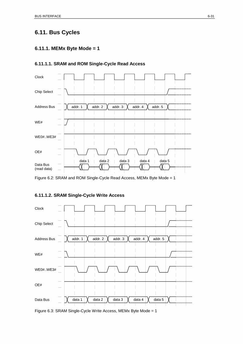
BUS INTERFACE 6-31
6.11. Bus Cycles
6.11.1. MEMx Byte Mode = 1
6.11.1.1. SRAM and ROM Single-Cycle Read Access
Clock
Chip Select
Address Bus
WE0#..WE3#
OE#
Data Bus(read data)
addr. 1 addr. 2 addr. 4addr. 3 addr. 5
data 1 data 2 data 3 data 4 data 5
WE#
Figure 6.2: SRAM and ROM Single-Cycle Read Access, MEMx Byte Mode = 1
6.11.1.2. SRAM Single-Cycle Write Access
Clock
Chip Select
Address Bus
WE0#..WE3#
OE#
Data Bus
addr. 1 addr. 2 addr. 4addr. 3 addr. 5
data 1 data 2 data 4data 3 data 5
WE#
Figure 6.3: SRAM Single-Cycle Write Access, MEMx Byte Mode = 1

6-32 CHAPTER 6
6.11.1.3. SRAM and ROM Multi-Cycle Read Access
Clock
Chip Select
Address Bus
WE0#..WE3#
OE#
Data Bus
Access time2..16 cycles
Addresssetup time0..3 cycles
Bus holdtime
0..7 cycles
WE#
Figure 6.4: SRAM and ROM Multi-Cycle Read Access, MEMx Byte Mode = 1
6.11.1.4. SRAM Multi-Cycle Write Access
Clock
Chip Select
Address Bus
WE0#..WE3#
OE#
Data Bus
Access time2..16 cycles
Addresssetup time0..3 cycles
Bus holdtime
0..7 cycles
WE#
Figure 6.5: SRAM Multi-Cycle Write Access, MEMx Byte Mode = 1
BUS INTERFACE 6-33
6.11.2. MEMx Byte Mode = 0
6.11.2.1. SRAM Single-Cycle Read Access
Clock
Chip Select
Address Bus
BE0#..BE3#
OE#
Data Bus(read data)
addr. 1 addr. 2 addr. 4addr. 3 addr. 5
data 1 data 2 data 3 data 4 data 5
WE#
Figure 6.6: SRAM Single-Cycle Read Access, MEMx Byte Mode = 0
6.11.2.2. SRAM Single-Cycle Write Access
Clock
Chip Select
Address Bus
BE0#..BE3#
OE#
Data Bus
addr. 1 addr. 2 addr. 4addr. 3 addr. 5
data 1 data 2 data 4data 3 data 5
WE#
Figure 6.7: SRAM Single-Cycle Write Access, MEMx Byte Mode = 0

6-34 CHAPTER 6
6.11.2.3. SRAM Multi-Cycle Read Access
Clock
Chip Select
Address Bus
BE0#..BE3#
OE#
Data Bus
Access time2..16 cycles
Addresssetup time0..3 cycles
Bus holdtime
0..7 cycles
WE#
Figure 6.8: SRAM Multi-Cycle Read Access, MEMx Byte Mode = 0
6.11.2.4. SRAM Multi-Cycle Write Access
Clock
Chip Select
Address Bus
BE0#..BE3#
OE#
Data Bus
Access time2..16 cycles
Addresssetup time0..3 cycles
Bus holdtime
0..7 cycles
WE#
Figure 6.9: SRAM Multi-Cycle Write Access, MEMx Byte Mode = 0
BUS INTERFACE 6-35
6.11.3. MEM2 Read Access with WAIT PinMEM2 Byte Mode = 1, INT3Polarity = Inverted,address setup time = 0 cycles, bus hold time = 0 cycles
Clock
Chip Select
Address Bus
WE0#..WE3#
OE#
Data Bus
Access time(minimum 4 cycles)
next accessor bus hold
time if specified
WAIT
Figure 6.10: MEM2 Read Access with WAIT Pin
Note:
Arrows on WAIT signal indicate the times where the signal is inspected.
In this examplespecified access time: 4 cyclesactual access time: 6 = 4 cycles + 2 additional cycles caused by WAIT pin
6-36 CHAPTER 6
6.11.4. I/O Read Access
Clock
Chip Select
Address Bus
WE#
IORD#
Data Bus
Access time2..16 cycles
Addresssetup time0..6 cycles
Bus holdtime
0..6 cycles
Figure 6.11: I/O Read Access

BUS INTERFACE 6-37
6.11.5. I/O Read Access with WAIT Pinaddress setup time = 0 cycles, bus hold time = 0 cycles, INT3Polarity = Inverted
Clock
Chip Select
Address Bus
WE#
IORD#
Data Bus
Access time(minimum 4 cycles)
next accessor bus hold
time if specified
WAIT
Figure 6.12: I/O Read Access with WAIT Pin
Note:
Arrows on WAIT signal indicate the times where the signal is inspected.
In this examplespecified access time: 4 cyclesactual access time: 6 = 4 cycles + 2 additional cycles caused by WAIT pin

6-38 CHAPTER 6
6.11.6. I/O Write Access
Clock
Chip Select
Address Bus
WE#
IORD#
Data Bus
Access time2..16 cycles
Addresssetup time0..6 cycles
Bus holdtime
1..7 cycles
IOWR#
Figure 6.13: I/O Write Access
Note:
If IORD# is used as I/O data strobe, IORD# instead of IOWR# is activated low.

BUS INTERFACE 6-39
6.11.7. DRAM
6.11.7.1. Fast Page Mode DRAM Access
Clock
Address Buslow order bits
RAS#
CAS0#..CAS3#
RAS to CAS delay time1..4 cycles
RAS precharge time1..6 cycles
CAS accesstime
1..6 cycles
Address Bushigh order bits
CAS accesstime
1..6 cycles
at read access
WE#
Data Bus(read data)
at write access
WE#
Data Bus(write data)
undefined row address col. addr. col. addr.
valid
OE#
OE#
Figure 6.14: Fast Page Mode DRAM Access

6-40 CHAPTER 6
6.11.7.2. EDO DRAM Single-Cycle Access
at write access
Clock
Address Buslow order bits
RAS#
CAS0#..CAS3#
RAS to CAS delay time1..4 cycles
RAS precharge time1..6 cycles
CAS accesstime
1..6 cycles
Address Bushigh order bits
CAS accesstime
1..6 cycles
at read access
WE#
Data Bus(read data)
WE#
Data Bus(write data)
undefined row address col. addr. col. addr.
valid
OE#
OE#
Figure 6.15: EDO DRAM Single-Cycle Access
BUS INTERFACE 6-41
6.11.7.3. EDO DRAM Multi-Cycle Access
at write access
Clock
Address Buslow order bits
RAS#
CAS0#..CAS3#
RAS to CAS delay time1..4 cycles
RASprecharge time
1..6 cycles
CAS access time1..6 cycles
Address Bushigh order bits
CAS access time1..6 cycles
at read access
WE#
Data Bus(read data)
WE#
Data Bus(write data)
undefined row addr. column address column address
valid
OE#
OE#
OE# is set after the first cycle of the CAS access time
Figure 6.16: EDO DRAM Multi-Cycle Access

6-42 CHAPTER 6
6.11.7.4. Fast Page Mode or EDO DRAM Refresh
Clock
Address Bus
CAS#
RAS to CAS delay time1..4 cycles
RAS precharge time1..6 cycles
CAS accesstime
1..6 cycles
RAS#
undefined
Figure 6.17: DRAM Refresh
Note:
The type of refresh that is performed is CAS Before RAS.
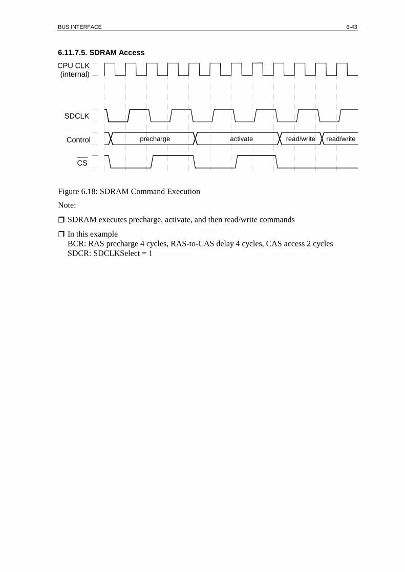
BUS INTERFACE 6-43
6.11.7.5. SDRAM AccessCPU CLK(internal)
Control
CS
SDCLK
precharge activate read/write read/write
Figure 6.18: SDRAM Command Execution
Note:
SDRAM executes precharge, activate, and then read/write commands
In this exampleBCR: RAS precharge 4 cycles, RAS-to-CAS delay 4 cycles, CAS access 2 cyclesSDCR: SDCLKSelect = 1

6-44 CHAPTER 6
6.12. DC Characteristics
Absolute Maximum Ratings
Case temperature TC under Bias: 0°C to +85°Cextended temperature range on request
Storage Temperature: -65°C to +150°C
Voltage on any Pin with respect to ground: -0.5V to + 3.8V
D.C. Parameters
Supply Voltage Core: 2.5V ± 5%
Supply Voltage I/O: 3.3V ± 10%
Case Temperature TCASE: 0°C to +70°C
Symbol Parameter Min Max Units Notes
VIL Input LOW Voltage -0.3 0.8 V except CLKIN
VIH Input HIGH Voltage 2.0 3.6 V except CLKIN
VOL Output LOW Voltage 0.45 V at 4mA
VOH Output HIGH Voltage 2.4 V at 1mA
ILI Input Leakage Current ±20 µA
ILO Output Leakage Current ±20 µA
CCLK Clock Capacitance 10 pF
CADR Output CapacitanceA12..A0
15 pF
CI/O Input/output Capacitanceall other signals
10 pF
Table 6.14: DC Characteristics

BUS INTERFACE 6-45
6.13. AC Characteristics
6.13.1. Processor Clock and CLKINThe maximum internal processor clock frequency of the hyperstone E1-32XS and E1-16XSis 115 MHz.
The internal PLL of the hyperstone E1-32XS and E1-16XS multiplies the clock at the inputpin CLKIN by ½, 1, 2, 4 or 8. Please be aware that the internal PLL can not operate with acrystal or a crystal oscillator of a frequency higher than 20 MHz.
CLK
tCLK
CLKIN
tCLKINWH tCLKINWL
tCLKIN
Figure 6.19: Internal Processor Clock CLK and CLKIN
Symbol Description Min Time(ns)
Max Time(ns)
Min Freq.(MHz)
Max Freq.(MHz)
tCLK CLK period 8.7 1000 1 115
tCLKIN CLKIN period 50 1000 1 25
tCLKINWH CLKIN high time 16 -
tCLKINWL CLKIN low time 16 -
Table 6.15: CLKIN Times
Note: CLKIN timing is referenced to 1.65V.
6.13.2. GRANT# response timeIf a GRANT# low to high transition is detected while the processor is in power-down modewith SDRAM connected, the release of the processor bus may be delayed until the nextSDRAM refresh cycle is scheduled (normally, every 16 µs). This only happens if theMem0 memory type is SDRAM.

6-46 CHAPTER 6
t blank.

MECHANICAL DATA 7-1
7. Mechanical Data
7.1. hyperstone E1-32XS, 144-Pin LQFP Package
7.1.1. Pin Configuration - View from Top Side 21 3 4 5 6 7 8 9 10 11 12 13 14 15 16 17 18 19 20 21 22 23 24 25
108
107
106
105
104
103
102
101
100 99 98 96 95 94 93 92 91 90 89 88 87 86 85
123124125126127128129130131132133
97
484746454443
71706968676665646362
4950
A20A21
GNDD31D30D29
A9A10A11A12
VCCD28D27D26
GNDD25D15D14
VCCD13D12D11D10
GNDVCC
GNDXTAL1/CLKINXTAL2IO2VCCD16D17D18A3A2A1A0GNDDP1DP0
CLKOUTIO1GNDRQSTINT4INT3/WAITINT2INT1GNDVCC
VCC
GN
DBO
OTB A1
8A1
7G
ND
int
VCC
int
A16
A15
A25
GN
DA2
4A2
3G
ND
int
VCC
int
A22
A8 A7VC
C A6 A5 A4G
ND
WE
0#/B
E0#
WE
1#/B
E1#
GN
D
GN
DD
8D
7VC
Cin
tG
ND
int
D6
D24
VCC
D23
D22
GN
DD
5D
4D
3VC
CD
2D
1D
0VC
Cin
tG
ND
int
D21
D20
84 83G
ND
D19
DP2
DP3
VCC
int
GN
Din
tR
ESE
T#G
RAN
T#VC
CG
ND
VCC
6160595857565554535251
VCCGNDWE3#/BE3#WE2#/BE2#IORD#OE#VCCCAS3#CAS2#CAS1#
26 27 28 29 30 31 32 33 34 35 36
VCC
CAS
0# A14
GN
Din
tVC
Cin
tAC
TA1
3G
ND
WE
#G
ND
VCC
134135136137138139140141142143144VCC
GNDIO3
IOWR#CS3#CS2#CS1#GND
RAS#A19
VCC
72
BOOTW
VCC
D9
hyperstoneE1-32XS
424140393837
82 81 80 79 78 77 76 75 74 73
109110111112113114115116117118119120121122
Figure 7.1: hyperstone E1-32XS, 144-Pin LQFP Package

7-2 CHAPTER 7
7.1.2. Pin Cross Reference by Pin Name Signal Location Signal Location Signal Location Signal Location
A0 58 CS3# 140 DP3 80 IOWR# 141 A1 57 D0 88 GND 2 OE# 42 A2 56 D1 89 GND 11 RAS# 136 A3 55 D2 90 GND 23 RESET# 77 A4 22 D3 92 GND 33 RQST 66 A5 21 D4 93 GND 35 VCC 1 A6 20 D5 94 GND 38 VCC 19 A7 18 D6 100 GND 47 VCC 26 A8 17 D7 103 GND 59 VCC 36 A9 127 D8 104 GND 65 VCC 37 A10 126 D9 106 GND 71 VCC 43 A11 125 D10 111 GND 74 VCC 51 A12 124 D11 112 GND 83 VCC 72 A13 32 D12 113 GND 95 VCC 73 A14 28 D13 114 GND 105 VCC 75 A15 9 D14 116 GND 107 VCC 91 A16 8 D15 117 GND 110 VCC 98 A17 5 D16 52 GND 119 VCC 108 A18 4 D17 53 GND 131 VCC 109 A19 135 D18 54 GND 137 VCC 115 A20 133 D19 82 GND 143 VCC 123 A21 132 D20 84 GNDint 6 VCC 134 A22 16 D21 85 GNDint 14 VCC 144 A23 13 D22 96 GNDint 29 VCCint 7 A24 12 D23 97 GNDint 78 VCCint 15 A25 10 D24 99 GNDint 86 VCCint 30 ACT 31 D25 118 GNDint 101 VCCint 79 BOOTB 3 D26 120 GRANT# 76 VCCint 87 BOOTW 62 D27 121 INT1 70 VCCint 102 CAS0# 27 D28 122 INT2 69 WE# 34 CAS1# 46 D29 128 INT3/WAIT 68 WE0#/BE0# 24 CAS2# 45 D30 129 INT4 67 WE1#/BE1# 25 CAS3# 44 D31 130 IO1 64 WE2#/BE2# 40 CLKOUT 63 DP0 61 IO2 50 WE3#/BE3# 39 CS1# 138 DP1 60 IO3 142 XTAL1/CLKIN 48 CS2# 139 DP2 81 IORD# 41 XTAL2 49

MECHANICAL DATA 7-3
7.1.3. Pin Cross Reference by Location Location Signal Location Signal Location Signal Location Signal
1 VCC 37 VCC 73 VCC 109 VCC 2 GND 38 GND 74 GND 110 GND 3 BOOTB 39 WE3#/BE3# 75 VCC 111 D10 4 A18 40 WE2#/BE2# 76 GRANT# 112 D11 5 A17 41 IORD# 77 RESET# 113 D12 6 GNDint 42 OE# 78 GNDint 114 D13 7 VCCint 43 VCC 79 VCCint 115 VCC 8 A16 44 CAS3# 80 DP3 116 D14 9 A15 45 CAS2# 81 DP2 117 D15 10 A25 46 CAS1# 82 D19 118 D25 11 GND 47 GND 83 GND 119 GND 12 A24 48 XTAL1/CLKIN 84 D20 120 D26 13 A23 49 XTAL2 85 D21 121 D27 14 GNDint 50 IO2 86 GNDint 122 D28 15 VCCint 51 VCC 87 VCCint 123 VCC 16 A22 52 D16 88 D0 124 A12 17 A8 53 D17 89 D1 125 A11 18 A7 54 D18 90 D2 126 A10 19 VCC 55 A3 91 VCC 127 A9 20 A6 56 A2 92 D3 128 D29 21 A5 57 A1 93 D4 129 D30 22 A4 58 A0 94 D5 130 D31 23 GND 59 GND 95 GND 131 GND 24 WE0#/BE0# 60 DP1 96 D22 132 A21 25 WE1#/BE1# 61 DP0 97 D23 133 A20 26 VCC 62 BOOTW 98 VCC 134 VCC 27 CAS0# 63 CLKOUT 99 D24 135 A19 28 A14 64 IO1 100 D6 136 RAS# 29 GNDint 65 GND 101 GNDint 137 GND 30 VCCint 66 RQST 102 VCCint 138 CS1# 31 ACT 67 INT4 103 D7 139 CS2# 32 A13 68 INT3/WAIT 104 D8 140 CS3# 33 GND 69 INT2 105 GND 141 IOWR# 34 WE# 70 INT1 106 D9 142 IO3 35 GND 71 GND 107 GND 143 GND 36 VCC 72 VCC 108 VCC 144 VCC

7-4 CHAPTER 7
7.2. hyperstone E1-16XS, 100-Pin LQFP Package
7.2.1. Pin Configuration - View from Top Side
21 3 4 5 6 7 8 9 10 11 12 13 14 15 16 17 18 19 20 21 22 23 24 25
75 74 73 72 71 70 69 68 67 66 65 63 62 61 60 59 58 57 56 55 54 5390919293949596979899100
64
373635343332
3839
A20A21
GNDA9
A10A11A12
VCCGNDD15D14VCCD13D12D11D10
GNDXTAL1/CLKINXTAL2IO2VCCA3A2A1A0GNDCLKOUTIO1GNDRQSTINT4INT3/WAITINT2INT1
BOO
TB A18
A17
GN
Din
tVC
Cin
tA1
6A1
5G
ND
GN
Din
tVC
Cin
tA8 A7
VCC A6 A5 A4
GN
D
GN
DD
8D
7VC
Cin
tG
ND
int
D6
GN
DD
5D
4D
3VC
CD
2D
1D
0VC
Cin
tG
ND
int
GN
D
VCC
int
GN
Din
tR
ESE
T#G
RAN
T#VC
C
WE1#/BE1#WE0#/BE0#IORD#OE#VCCCAS1#CAS0#
VCC
A14
GN
Din
tVC
Cin
tAC
TA1
3G
ND
WE
#
IO3IOWR#
CS3#CS2#CS1#GND
RAS#A19
VCC
50
D9
hyperstoneE1-16XS
313029282726
77
7980818283848586878889
76
78 4847
49
46454443424140
52 51
DP0
DP1
Figure 7.2: hyperstone E1-16XS, 100-Pin LQFP Package
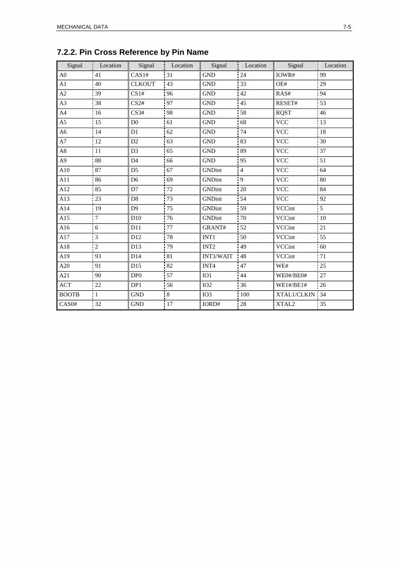
MECHANICAL DATA 7-5
7.2.2. Pin Cross Reference by Pin Name Signal Location Signal Location Signal Location Signal Location
A0 41 CAS1# 31 GND 24 IOWR# 99 A1 40 CLKOUT 43 GND 33 OE# 29 A2 39 CS1# 96 GND 42 RAS# 94 A3 38 CS2# 97 GND 45 RESET# 53 A4 16 CS3# 98 GND 58 RQST 46 A5 15 D0 61 GND 68 VCC 13 A6 14 D1 62 GND 74 VCC 18 A7 12 D2 63 GND 83 VCC 30 A8 11 D3 65 GND 89 VCC 37 A9 88 D4 66 GND 95 VCC 51 A10 87 D5 67 GNDint 4 VCC 64 A11 86 D6 69 GNDint 9 VCC 80 A12 85 D7 72 GNDint 20 VCC 84 A13 23 D8 73 GNDint 54 VCC 92 A14 19 D9 75 GNDint 59 VCCint 5 A15 7 D10 76 GNDint 70 VCCint 10 A16 6 D11 77 GRANT# 52 VCCint 21 A17 3 D12 78 INT1 50 VCCint 55 A18 2 D13 79 INT2 49 VCCint 60 A19 93 D14 81 INT3/WAIT 48 VCCint 71 A20 91 D15 82 INT4 47 WE# 25 A21 90 DP0 57 IO1 44 WE0#/BE0# 27 ACT 22 DP1 56 IO2 36 WE1#/BE1# 26 BOOTB 1 GND 8 IO3 100 XTAL1/CLKIN 34 CAS0# 32 GND 17 IORD# 28 XTAL2 35
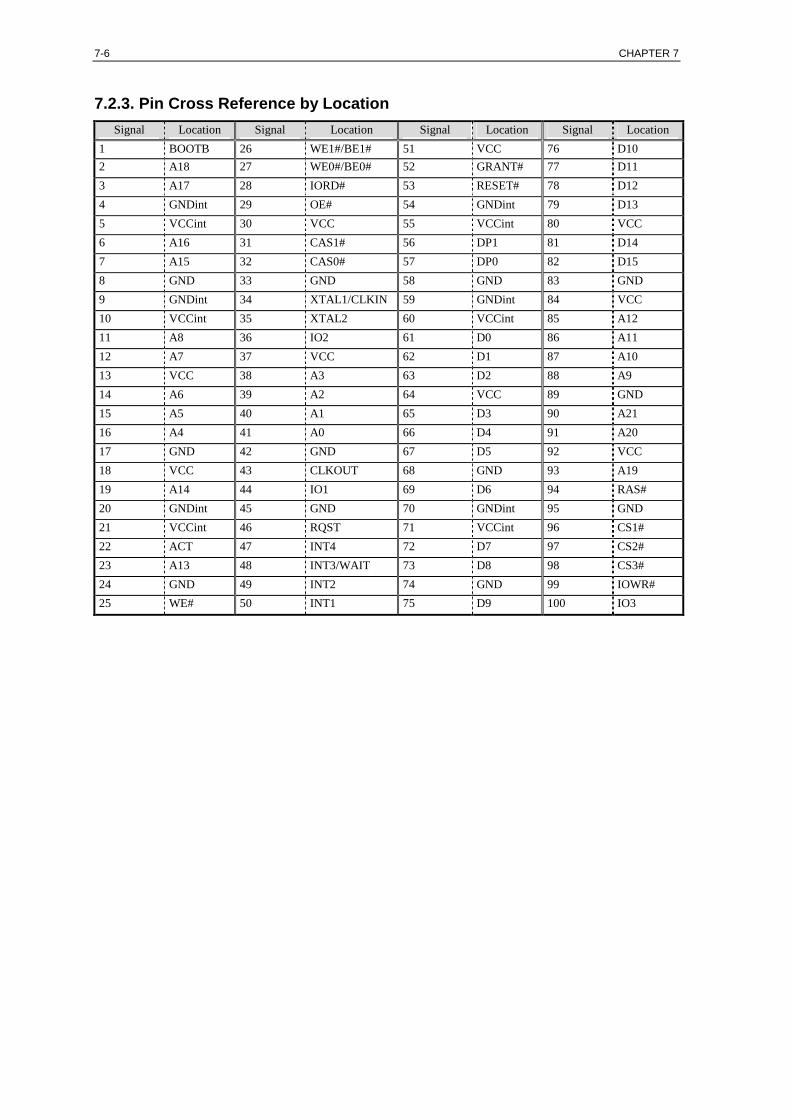
7-6 CHAPTER 7
7.2.3. Pin Cross Reference by Location Signal Location Signal Location Signal Location Signal Location
1 BOOTB 26 WE1#/BE1# 51 VCC 76 D10 2 A18 27 WE0#/BE0# 52 GRANT# 77 D11 3 A17 28 IORD# 53 RESET# 78 D12 4 GNDint 29 OE# 54 GNDint 79 D13 5 VCCint 30 VCC 55 VCCint 80 VCC 6 A16 31 CAS1# 56 DP1 81 D14 7 A15 32 CAS0# 57 DP0 82 D15 8 GND 33 GND 58 GND 83 GND 9 GNDint 34 XTAL1/CLKIN 59 GNDint 84 VCC 10 VCCint 35 XTAL2 60 VCCint 85 A12 11 A8 36 IO2 61 D0 86 A11 12 A7 37 VCC 62 D1 87 A10 13 VCC 38 A3 63 D2 88 A9 14 A6 39 A2 64 VCC 89 GND 15 A5 40 A1 65 D3 90 A21 16 A4 41 A0 66 D4 91 A20 17 GND 42 GND 67 D5 92 VCC 18 VCC 43 CLKOUT 68 GND 93 A19 19 A14 44 IO1 69 D6 94 RAS# 20 GNDint 45 GND 70 GNDint 95 GND 21 VCCint 46 RQST 71 VCCint 96 CS1# 22 ACT 47 INT4 72 D7 97 CS2# 23 A13 48 INT3/WAIT 73 D8 98 CS3# 24 GND 49 INT2 74 GND 99 IOWR# 25 WE# 50 INT1 75 D9 100 IO3
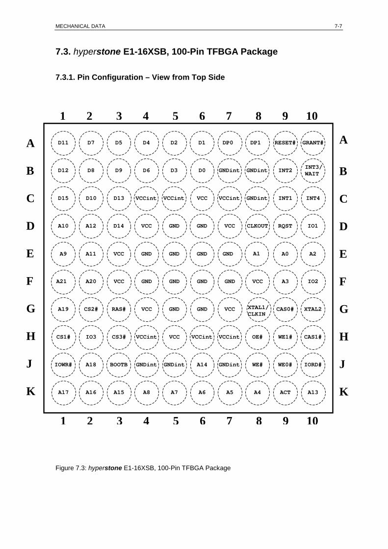
MECHANICAL DATA 7-7
7.3. hyperstone E1-16XSB, 100-Pin TFBGA Package
7.3.1. Pin Configuration – View from Top Side
0
I
K
1 2 3 4 5 6 7 8 9 1
F
D11 D7 D5 D4 D2 D1 DP0 DP1 RESET# GRANT#
D12 D8 D9 D6 D3 D0 GNDint GNDint INT2INT3/WAIT
D15 D10 D13 VCCint VCCint VCC VCCint GNDint INT1 INT4
A10 A12 D14 VCC GND GND VCC CLKOUT RQST IO1
A9 A11 VCC GND GND GND GND A1 A0 A2
A21 A20 VCC GND GND GND GND VCC A3 IO2
A19 CS2# RAS# VCC GND GND VCC XTAL1/CLKIN
CAS0# XTAL2
CS1# IO3 CS3# VCCint VCC VCCint VCCint OE# WE1# CAS1#
OWR# A18 BOOTB GNDint GNDint A14 GNDint WE# WE0# IORD#
A17 A16 A15 A8 A7 A6 A5 A4 ACT A13
A
B
C
D
E
F
G
H
J
K
1 2 3 4 5 6 7 8 9 10
A
B
C
D
E
F
G
H
J
igure 7.3: hyperstone E1-16XSB, 100-Pin TFBGA Package

7-8 CHAPTER 7
7.3.2. Pin Cross Reference by Pin Name Signal Location Signal Location Signal Location Signal Location
A0 E9 CAS1# H10 GND E4 IOWR# J1 A1 E8 CLKOUT D8 GND E5 OE# H8 A2 E10 CS1# H1 GND E6 RAS# G3 A3 F9 CS2# G2 GND E7 RESET# A9 A4 K8 CS3# H3 GND F4 RQST D9 A5 K7 D0 B6 GND F5 VCC C6 A6 K6 D1 A6 GND F6 VCC D4 A7 K5 D2 A5 GND F7 VCC D7 A8 K4 D3 B5 GND G5 VCC E3 A9 E1 D4 A4 GND G6 VCC F3 A10 D1 D5 A3 GNDint B7 VCC F8 A11 E2 D6 B4 GNDint B8 VCC G4 A12 D2 D7 A2 GNDint C8 VCC G7 A13 K10 D8 B2 GNDint J4 VCC H5 A14 J6 D9 B3 GNDint J5 VCCint C4 A15 K3 D10 C2 GNDint J7 VCCint C5 A16 K2 D11 A1 GRANT# A10 VCCint C7 A17 K1 D12 B1 INT1 C9 VCCint H4 A18 J2 D13 C3 INT2 B9 VCCint H6 A19 G1 D14 D3 INT3/WAIT B10 VCCint H7 A20 F2 D15 C1 INT4 C10 WE# J8 A21 F1 DP0 A7 IO1 D10 WE0# J9 ACT K9 DP1 A8 IO2 F10 WE1# H9 BOOTB J3 GND D5 IO3 H2 XTAL1/CLKIN G8 CAS0# G9 GND D6 IORD# J10 XTAL2 G10
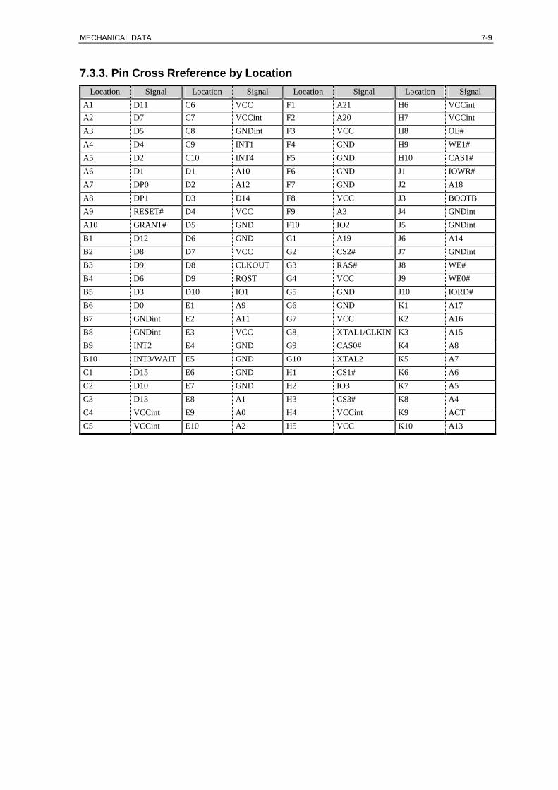
MECHANICAL DATA 7-9
7.3.3. Pin Cross Rreference by Location Location Signal Location Signal Location Signal Location Signal
A1 D11 C6 VCC F1 A21 H6 VCCint A2 D7 C7 VCCint F2 A20 H7 VCCint A3 D5 C8 GNDint F3 VCC H8 OE# A4 D4 C9 INT1 F4 GND H9 WE1# A5 D2 C10 INT4 F5 GND H10 CAS1# A6 D1 D1 A10 F6 GND J1 IOWR# A7 DP0 D2 A12 F7 GND J2 A18 A8 DP1 D3 D14 F8 VCC J3 BOOTB A9 RESET# D4 VCC F9 A3 J4 GNDint A10 GRANT# D5 GND F10 IO2 J5 GNDint B1 D12 D6 GND G1 A19 J6 A14 B2 D8 D7 VCC G2 CS2# J7 GNDint B3 D9 D8 CLKOUT G3 RAS# J8 WE# B4 D6 D9 RQST G4 VCC J9 WE0# B5 D3 D10 IO1 G5 GND J10 IORD# B6 D0 E1 A9 G6 GND K1 A17 B7 GNDint E2 A11 G7 VCC K2 A16 B8 GNDint E3 VCC G8 XTAL1/CLKIN K3 A15 B9 INT2 E4 GND G9 CAS0# K4 A8 B10 INT3/WAIT E5 GND G10 XTAL2 K5 A7 C1 D15 E6 GND H1 CS1# K6 A6 C2 D10 E7 GND H2 IO3 K7 A5 C3 D13 E8 A1 H3 CS3# K8 A4 C4 VCCint E9 A0 H4 VCCint K9 ACT C5 VCCint E10 A2 H5 VCC K10 A13
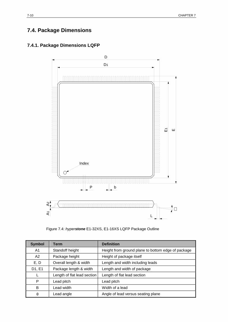
7-10 CHAPTER 7
7.4. Package Dimensions
7.4.1. Package Dimensions LQFP
b
D
D1
E1
Index
A1
A2
L
E
P
Figure 7.4: hyperstone E1-32XS, E1-16XS LQFP Package Outline
Symbol Term Definition A1 Standoff height Height from ground plane to bottom edge of package A2 Package height Height of package itself
E, D Overall length & width Length and width including leads D1, E1 Package length & width Length and width of package
L Length of flat lead section Length of flat lead section P Lead pitch Lead pitch B Lead width Width of a lead θ Lead angle Angle of lead versus seating plane
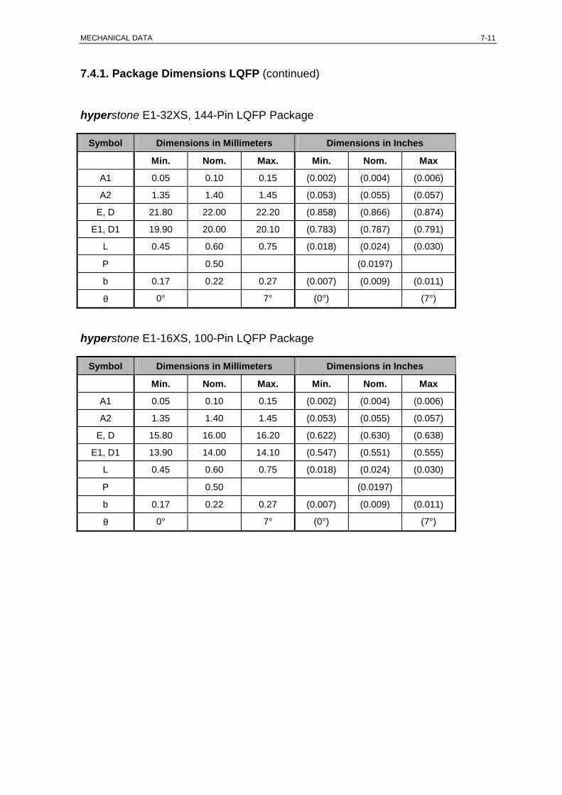
MECHANICAL DATA 7-11
7.4.1. Package Dimensions LQFP (continued)
hyperstone E1-32XS, 144-Pin LQFP Package
Symbol Dimensions in Millimeters Dimensions in Inches
Min. Nom. Max. Min. Nom. Max
A1 0.05 0.10 0.15 (0.002) (0.004) (0.006)
A2 1.35 1.40 1.45 (0.053) (0.055) (0.057)
E, D 21.80 22.00 22.20 (0.858) (0.866) (0.874)
E1, D1 19.90 20.00 20.10 (0.783) (0.787) (0.791)
L 0.45 0.60 0.75 (0.018) (0.024) (0.030)
P 0.50 (0.0197)
b 0.17 0.22 0.27 (0.007) (0.009) (0.011)
θ 0° 7° (0°) (7°)
hyperstone E1-16XS, 100-Pin LQFP Package
Symbol Dimensions in Millimeters Dimensions in Inches
Min. Nom. Max. Min. Nom. Max
A1 0.05 0.10 0.15 (0.002) (0.004) (0.006)
A2 1.35 1.40 1.45 (0.053) (0.055) (0.057)
E, D 15.80 16.00 16.20 (0.622) (0.630) (0.638)
E1, D1 13.90 14.00 14.10 (0.547) (0.551) (0.555)
L 0.45 0.60 0.75 (0.018) (0.024) (0.030)
P 0.50 (0.0197)
b 0.17 0.22 0.27 (0.007) (0.009) (0.011)
θ 0° 7° (0°) (7°)
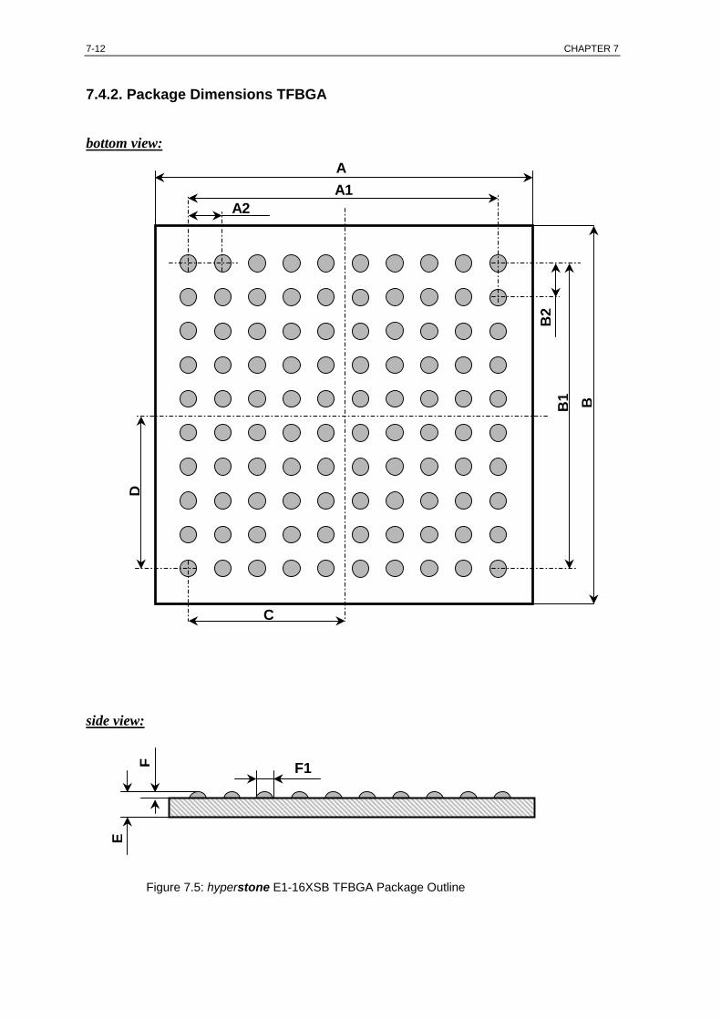
7-12 CHAPTER 7
7.4.2. Package Dimensions TFBGA
bottom view:
side view:
Figure 7.5: hyperstone E1-16XSB TFBGA Package Outline
AA1
A2
BB1
B2
C
D
F1F
E
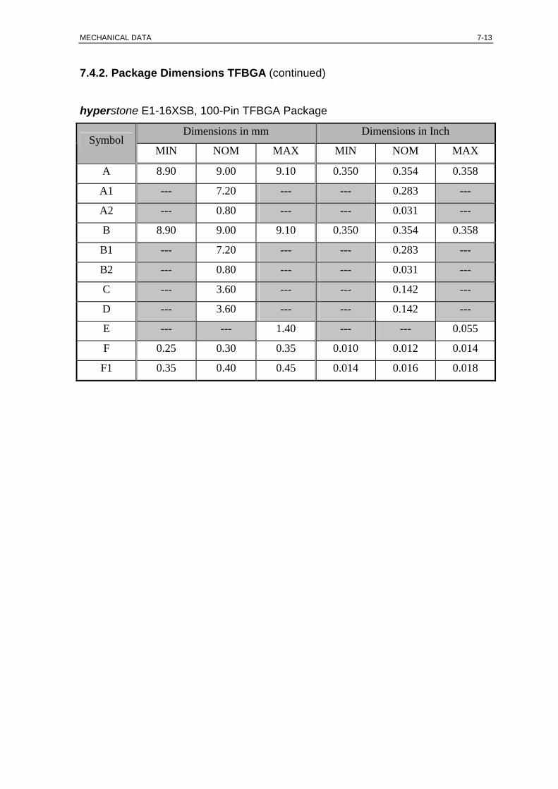
MECHANICAL DATA 7-13
7.4.2. Package Dimensions TFBGA (continued)
hyperstone E1-16XSB, 100-Pin TFBGA Package
Dimensions in mm Dimensions in Inch Symbol
MIN NOM MAX MIN NOM MAX
A 8.90 9.00 9.10 0.350 0.354 0.358
A1 --- 7.20 --- --- 0.283 ---
A2 --- 0.80 --- --- 0.031 ---
B 8.90 9.00 9.10 0.350 0.354 0.358
B1 --- 7.20 --- --- 0.283 ---
B2 --- 0.80 --- --- 0.031 ---
C --- 3.60 --- --- 0.142 ---
D --- 3.60 --- --- 0.142 ---
E --- --- 1.40 --- --- 0.055
F 0.25 0.30 0.35 0.010 0.012 0.014
F1 0.35 0.40 0.45 0.014 0.016 0.018

7-14 CHAPTER 7

SPECIFICATION CHANGES 8-1
8. Specification ChangesCompared to the specifications in this manual, the currently available E1-32XS and E1-16XS chips have three limitations. This includes, but is not limited to the lot numbers
K60062.1
K60172.1.*
The specification differences are listed in the following sections.
8.1. Clock SpeedThe maximum clock speed is 110 MHz, the maximum XTAL1 input frequency is 20 MHz.
8.2. SDRAM Clock ModeThe delayed SDRAM clock mode is not available, the non-delayed SDRAM clock modemust be used.
8.3. GRANT# Response TimeIf a GRANT# low to high transition is detected while the processor is in power-downmode, the release of the processor bus may be delayed until the next SDRAM refresh cycleis scheduled (normally, every 16 µs). This only happens if the Mem0 memory type isSDRAM.

8-2 CHAPTER 8