hybrid metal semiconductor article nanostructure for...
TRANSCRIPT
NARASIMHAN ET AL. VOL. XXX ’ NO. XX ’ 000–000 ’ XXXX
www.acsnano.org
A
CXXXX American Chemical Society
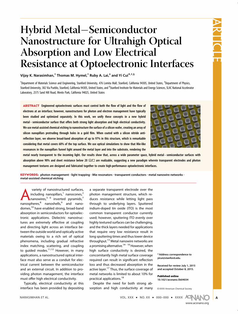
Hybrid Metal�SemiconductorNanostructure for Ultrahigh OpticalAbsorption and Low ElectricalResistance at Optoelectronic InterfacesVijay K. Narasimhan,† Thomas M. Hymel,† Ruby A. Lai,‡ and Yi Cui*,†,§
†Department of Materials Science and Engineering, Stanford University, 476 Lomita Mall, Stanford, California 94305, United States, ‡Department of Physics,Stanford University, 382 Via Pueblo, Stanford, California 94305, United States, and §Stanford Institute for Materials and Energy Sciences, SLAC National AcceleratorLaboratory, 2575 Sand Hill Road, Menlo Park, California 94025, United States
Avariety of nanostructured surfaces,including nanopillars,1 nanocones,2
nanowires,3�6 inverted pyramids,7
nanospheres,8 nanoshells,9 and nano-domes,10 have enabled strong, broad-bandabsorption in semiconductors for optoelec-tronic applications. Dielectric nanostruc-tures are extremely effective at couplingand directing light across an interface be-tween the outsideworld and optically activematerials owing to a rich set of opticalphenomena, including gradual refractiveindex matching, scattering, and couplingto guided modes.11,12 However, in manyapplications, a nanostructured optical inter-face must also serve as a conduit for elec-trical current between the semiconductorand an external circuit. In addition to pro-viding photon management, the interfacemust offer high electrical conductivity.Typically, electrical conductivity at this
interface has been provided by depositing
a separate transparent electrode over thephoton management structure, which re-duces resistance while letting light passthrough to underlying layers. Sputteredindium-doped tin oxide (ITO) is the mostcommon transparent conductor currentlyused; however, sputtering ITO evenly overhighly textured surfaces can be challenging,and the thick layers needed for applicationsthat require very low resistance result inlong sputtering times and thus lower devicethroughput.13 Metal nanowire networks area promising alternative.14�16However, whenhigh surface conductivity is desired, theconcomitantly high metal surface coveragerequired can result in significant reflectionloss and thus decreased absorption in theactive layer.17 Thus, the surface coverage ofmetal networks is limited to about 10% forpractical applications.18
Despite the need for both strong ab-sorption and high conductivity at many
* Address correspondence [email protected].
Received for review July 1, 2015and accepted October 8, 2015.
Published online10.1021/acsnano.5b04034
ABSTRACT Engineered optoelectronic surfaces must control both the flow of light and the flow of
electrons at an interface; however, nanostructures for photon and electron management have typically
been studied and optimized separately. In this work, we unify these concepts in a new hybrid
metal�semiconductor surface that offers both strong light absorption and high electrical conductivity.
We use metal-assisted chemical etching to nanostructure the surface of a silicon wafer, creating an array of
silicon nanopillars protruding through holes in a gold film. When coated with a silicon nitride anti-
reflection layer, we observe broad-band absorption of up to 97% in this structure, which is remarkable
considering that metal covers 60% of the top surface. We use optical simulations to show that Mie-like
resonances in the nanopillars funnel light around the metal layer and into the substrate, rendering the
metal nearly transparent to the incoming light. Our results show that, across a wide parameter space, hybrid metal�semiconductor surfaces with
absorption above 90% and sheet resistance below 20 Ω/0 are realizable, suggesting a new paradigm wherein transparent electrodes and photon
management textures are designed and fabricated together to create high-performance optoelectronic interfaces.
KEYWORDS: photon management . light trapping . Mie resonators . transparent conductors . metal nanowire networks .metal-assisted chemical etching
ARTIC
LE

NARASIMHAN ET AL. VOL. XXX ’ NO. XX ’ 000–000 ’ XXXX
www.acsnano.org
B
optoelectronic interfaces and the commensurate sizescale of semiconductor photon management struc-tures and metal nanowire networks, these nanostruc-tured materials have been studied and developed inrelative isolation. In particular, the transparency ofmetal nanowire networks is optimized and measuredconsidering the network in isolation, that is, suspendedin free space or sometimes on a transparent substrate.At real interfaces with nanostructured semiconductors,
the profile of the light, and therefore the performanceof the network, could differ significantly. Here, wedemonstrate that unifying a metal nanowire gridwith extremely high surface coverage and a photonmanagement texture in a single optoelectronic inter-face can simultaneously improve optical absorptionand electrical conductivity, overcoming the conven-tional trade-offs encountered when designing thesestructures separately.
Figure 1. Comparison of perforated gold films on silicon substrates with and without silicon nanopillars protruding throughthe holes. (a) Schematic, (b) false-color 25� tilted-viewSEM (scale bar = 500nm,withgold in yellow), and (c) digital photograph(scale bar = 1 mm) for a 16 nm thick gold grid sitting atop a planar silicon substrate. The surface, which is 65% covered bymetal, is highly reflective. (d) Schematic, (e) false-color 25� tilted-view SEM micrograph (scale bar = 500 nm, with gold inyellow), and (f) digital photograph (scale bar = 1mm) for an identical 16 nm thick gold filmwith silicon nanopillars protrudingthrough the holes. The patterned area is dark red, indicating a significant decrease in reflection. (g) Angle-integratedreflection spectra of perforated metal films with (dashed blue trace) and without (dotted red trace) protruding siliconnanopillars. The perforated gold film on the planar substrate exhibits 50% integrated reflection averaged over the solarspectrum, while the film with protruding silicon nanopillars has only 19% reflection. The reflection can be further reduced to10% by coating the metal�silicon nanopillar sample with a 50 nm silicon nitride antireflection layer (solid black trace).
ARTIC
LE

NARASIMHAN ET AL. VOL. XXX ’ NO. XX ’ 000–000 ’ XXXX
www.acsnano.org
C
Our design is based on nanopillars with small aspectratios (∼1:1). These structures have been shown to actas broad-band light “funnels” by strongly coupling andconfining light into Mie-like resonances that leak intothe substrate through the small volume beneath eachpillar.19�21 By aligning nanopillars protruding froma substrate through the holes in a metal film, weexpected that most of the electric field intensity wouldbe concentrated in the nanopillars and thus not overareas of the substrate covered by the metal. Therefore,we hypothesized that even in metal films with highsurface coverage and small holes, the introduction ofdielectric nanopillars would substantially reduce thereflection losses from the metal, allowing light to beeasily absorbed in the underlying substrate.
RESULTS
We began by examining the optical properties of ahigh-surface-coverage metal film perforated withnanoscale holes sitting on top of a planar silicon sub-strate. Figure 1a,b shows a schematic and the scanningelectron micrograph (SEM) of a 16 nm thick gold filmpatterned with an array of 295 nm � 295 nm squareholes with a center-to-center spacing of 500 nm. Thepatterned film on the planar silicon substrate appearsshiny and reflective, only slightly darker than theunperforated gold areas surrounding it (Figure 1c). Thisappearance is expected considering the high surfacecoverage of the metal: 65% of the silicon surface iscovered with gold.Next, we examined the properties of an identical
gold film with silicon nanopillars protruding from thesubstrate through the holes. We fabricated this struc-ture with metal-assisted chemical etching (MACE),22
using the patterned gold film to anisotropically etchthe silicon. This process is described in more detailin the Methods section and shown schematically inFigure 2. The gold acts as a catalyst for the etching ofsilicon, and thus the gold film sinks into the substrate,creating an array of nanopillars that protrude throughholes in the film. The silicon nanopillars are thusautomatically aligned to the holes in the metal film ina single step.
Figure 1d,e shows a gold film identical to that shownin Figure 1a,b through which an array of silicon nano-pillars protrudes from the substrate 330 nm above themetal film. The change in the optical properties of thissurface is dramatic; the patterned area in the etchedsample with protruding nanopillars is a deep red color(Figure 1f).We measured the combined specular and diffuse
reflection (R) of the gold�silicon surfaces at differentangles of incidence. The reflection spectra of the twosamples confirms the dramatic change conferred bythe nanopillar array (Figure 1g): the perforated filmon the planar substrate reflects, on average, 50% ofthe incident light, whereas the etched sample withprotruding silicon nanopillars reflects only 19% of thelight. By adding a 50 nm thick silicon nitride anti-reflection coating, the reflection of the nanopillarsample decreases further, to 10%. Considering thatthe gold film still occupies 65%of the top surface of thesilicon in these samples, the magnitude of the changein the reflectance is surprising.To explain the remarkable optical properties of the
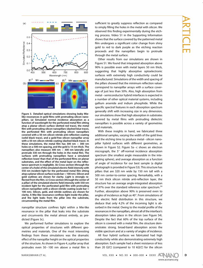
film, we next performed detailed simulations of amodel of our structure using S4, a freely available fre-quency modal method software package.23 Figure 3ashows the simulated reflection spectra for a siliconsubstratewith ametal filmwith 300nmwide holes on a500 nm spacing with a 15 nm thick gold layer, with andwithout protruding silicon nanopillars. The surfacewith nanopillars protruding 330 nm above the metaldemonstrates much less reflection, confirming ourexperimental observations. Moreover, Figure 3a alsoshows the simulated reflection spectra for a structurecoated with a 50 nm thick silicon nitride layer, bothwith and without the embedded metal film. Thedifference is negligible (2%), suggesting, as hypothe-sized, that the presence of the metal does not have asignificant impact on the optical properties of thisarchitecture. We also simulated the electric field pat-terns in the structures. Field patterns at an incidentwavelength of 550 nmare also shown in Figure 3.Whilethe patternedmetal film sitting on top of a planar siliconsurface strongly reflects incoming light (Figure 3b), the
Figure 2. Metal-assisted chemical etching process. (a) Process flow illustrating the key steps for fabricating a gold film withprotruding silicon nanopillars using metal-assisted chemical etching. A silicon substrate with a patterned gold film isimmersed into a solution of hydrofluoric acid and hydrogen peroxide to create the nanopillar array. (b) Detailed schematic ofthe etching step. The silicon directly beneath the gold layer is oxidized and attacked, resulting in the metal layer sinking intothe substrate. The silicon nanopillars are thus self-aligned with the holes in the metal film.
ARTIC
LE
NARASIMHAN ET AL. VOL. XXX ’ NO. XX ’ 000–000 ’ XXXX
www.acsnano.org
D
nanopillar structure confines light within a Mie-likeresonance in the pillar that leaks into the substrateand circumvents the metal almost entirely, as pre-dicted (Figure 3c).We performed further simulations to explore the
optical properties of structures with different geo-metries and materials. One of the most interestingfindings from these simulations was the dramaticeffect of the nanopillar height on the optical propertiesof the structure. As shown in Figure 4, a pillar array thatprotrudes even 50�100 nm above a metal film is
sufficient to greatly suppress reflection as comparedto simply filling the holes in the metal with silicon. Weobserved this finding experimentally during the etch-ing process. Video S1 in the Supporting Informationshows that the surface covered by the patternedmetalfilm undergoes a significant color change from shinygold to red to dark purple as the etching reactionproceeds and the nanopillars begin to protrudethrough the metal surface.Other results from our simulations are shown in
Figure S1. We found that integrated absorption above90% is possible even with metal layers 50 nm thick,suggesting that highly absorptive optoelectronicsurfaces with extremely high conductivity could bemanufactured. Simulations of the width and spacing ofthe pillars showed that the minimum reflection valuescorrespond to nanopillar arrays with a surface cover-age of just less than 50%. Also, high absorption frommetal�semiconductor hybrid interfaces is expected ina number of other optical material systems, includinggallium arsenide and indium phosphide. While thespecific spectral features in each absorption spectrumgenerally shift with increasing size in any dimension,our simulations show that high absorption in substratescovered by metal films with protruding dielectricnanopillars is possible across a variety of geometriesand materials.With these insights in hand, we fabricated three
additional samples, varying the width of the gold linesand the etching time to produce metal�silicon nano-pillar hybrid surfaces with different geometries, asshown in Figure S2. Figure 5a�c shows an electronmicrograph, the 5� off-normal incidence absorptionspectrum (the smallest angle measurable in the inte-grating sphere), and average absorption as a functionof angle of incidence for our best sample (a digitalphotograph is provided in Figure S3). This structure haspillars that are 320 nm wide by 150 nm tall with a500 nm center-to-center spacing. Remarkably, with a50 nm thick silicon nitride anti-reflection layer, thestructure has an average angle-integrated absorptionof 97% over the standard reference solar spectrum.24
Further, absorption above 90% is preserved even toangles of incidence as high as 40�. From simulations ofthe electric field distribution in this structure, wededuce that only 4.2% of the incoming light is ab-sorbed in the metal. Owing to the modal profile of theresonances in the nanopillars, almost all of the interface'sabsorption takes place in the silicon (see Figure S4).Despite the fact that 60% of the top surface of thesilicon is covered with a metal film, the structure dem-onstrates strong, broad-band absorption across thevisible spectrum and at a variety of angles of incidence.All four hybrid surfaces we fabricated had high
conductivity while also demonstrating extremely highabsorption. Each sample had a sheet resistance of lessthan 20 Ω/0 (compared to 10 kΩ/0 for the silicon
Figure 3. Detailed optical simulations showing leaky Mie-like resonances in gold films with protruding silicon nano-pillars. (a) Simulated normal incidence absorption as afunction of wavelength for the perforatedmetal film sittingatop a planar silicon surface (dotted red trace), the metalfilm with protruding silicon nanopillars (dashed blue trace),the perforated film with protruding silicon nanopillarscovered with a 50 nm silicon nitride anti-reflection coating(solid black trace), and a gold-free silicon nanopillar arraywith a 50 nm silicon nitride coating (dashed black trace). Inthese simulations, the metal film has 300 nm � 300 nmholes on a 500 nm spacing, and the gold is 15 nm thick. Thenanopillars also measure 300 nm � 300 nm laterally andprotrude 330 nm through the holes in the metal film. Thesurfaces with protruding nanopillars have a simulatedreflection lower than that of the perforated films on planarsubstrates, and the effect of the metal layer on the reflec-tance spectrum is negligible. (b) Cross section (through thecenter of a hole) of the simulated electric field intensity with550 nm incident light for the perforated metal film sittingatop aplanar silicon surface (scale bar = 100nm). Silicon andgold outlines are shown for clarity. Light is strongly re-flected from the film. (c) Cross section (through the center ofa pillar) of the simulated electric field intensity with 550 nmincident light for the perforated gold film with protrudingsilicon nanopillars with a silicon nitride coating (scale bar =100 nm). Silicon, gold, and nitride outlines are shown forclarity. A Mie-like resonance confines light inside the pillar,and the light leaks from the pillar into the substrate,circumventing the metal film.
ARTIC
LE

NARASIMHAN ET AL. VOL. XXX ’ NO. XX ’ 000–000 ’ XXXX
www.acsnano.org
E
substrates with the native oxide removed). Thesevalues were possible owing to the highmetal coverageof over 40%. Despite the high metal coverage, all thesamples demonstrated more than 89% absorptionaveraged over the standard reference solar spectrum24
from 400 to 900 nm (compared to 61% for the baresilicon substrate). In fact, the performance of theoptoelectronic interfaces we designed is equivalentto placing the highest performing transparent elec-trodes from the literature atop semiconductors coatedwith an ideal anti-reflection coating (see Figure S5).To demonstrate the potential of a metal�silicon
hybrid nanostructure in an optoelectronic device, wecompare the front surface reflectance between 400 and900 nm of the interface in Figure 5 with the reportedfront surface reflectance of a PERC-type silicon solarcell with front metal contacts25 in Figure S6. Thereference silicon solar cell shows a front surface reflec-tance of 6.5% averaged over the standard referencesolar spectrum compared to 2.8% from the gold�silicon hybrid structure. Remarkably, despite its lowerreflectance, the metal�silicon hybrid interface hasclose to 12 times the metal coverage of the referencesolar cell (60% versus 5.1%). Even including the calcu-lated 4.2% absorption loss in the metal, the opticallosses of the hybrid structure are comparable to thoseof the silicon solar cell (the absorption losses of thefront metal contacts were not reported directly forthe reference cell). The advantage of enabling highermetal coverage in a solar cell while maintaining similaroptical performance is that the series resistance couldbe substantially reduced. For example, the lateralresistance in the emitter comprises one-sixth of thetotal series resistance in the reference PERC solar cell;by providing a high-coverage grid with nanoscale
lines, this resistance (0.1 Ω cm2) could essentially beeliminated. With an appropriate metal contact stack,the nearly continuous metal coverage of the metal�silicon hybrid interface could thus result in a higher fillfactor while maintaining the same short circuit current.
Figure 4. Effect of the nanopillar height on simulatedreflection. The simulated short-wavelength reflectancefrom a perforated metal film with silicon filling its holes(dotted red trace) is still very high, whereas reflection dropssignificantly if the silicon protrudes 50 nm (dashed bluetrace) or 100 nm (solid black trace) above themetal surface.For these simulations, we assumed 200 nm square holeswith a 450 nm center-to-center spacing in a 50 nm thickmetal film. All structureswere assumed to be coveredwith a50 nm thick silicon nitride coating.
Figure 5. Optical characterization of the best performinghybrid metal�silicon nanopillar interface. (a) Tilted-viewSEM micrograph (scale bar = 500 nm). In this structure, thenanopillars are 320 nmwidewith a 500 nm center-to-centerspacing and protrude 150 nm from the 16 nm thick goldfilm. (b) 5� Off-normal absorption spectrum for bare silicon(dotted red trace), the as-made gold�silicon nanopillarsurface shown in (a) (dashed blue trace), and the gold�silicon nanopillar surface covered with a 50 nm siliconnitride coating (solid black trace). (c) Absorption of thegold�silicon nanopillar hybrid surface with a 50 nm siliconnitride coating as a function of incident light angle, aver-aged over the standard hemispherical reference solar spec-trum.24 Absorption as high as 97% is observed in thissample, and absorption above 90% is preserved even athigh angles of up to 40� from the normal even though 60%of the top surface is covered with gold.
ARTIC
LE

NARASIMHAN ET AL. VOL. XXX ’ NO. XX ’ 000–000 ’ XXXX
www.acsnano.org
F
However, the contact-emitter resistance and the surfacepassivation of the nanostructure would need to becarefully considered to ensure improved efficiency.
DISCUSSION
There are a variety of applications in which high-coverage metal films with nanoscale holes would bedesirable to provide dense, highly conductive electricalpathways to a semiconductor. These include electro-des for photosensors, solar cells, light-emitting diodes(LEDs), and displays;26 conductive patches for trans-parent antennas;27 interconnects for fully transparentelectronics;28 and even current collectors for transpar-ent batteries.29 However, to date, there has been noway to cover a semiconductor surface with a highfraction of metal without incurring significant reflec-tion loss at the interface. Only plasmonic resonanceshave been extensively studied for achieving extra-ordinary transmission through high-coverage metalfilms,30�32 and these resonances are very sensitiveto the shape and size of the holes.33�35 Plasmon-mediated extraordinary transmission is fairly narrow-band and polarization-sensitive; even state of the artstructures report only 50�80% transmission36,37 forcertain colors and greatly suppressed transmission inthe rest of the spectrum. By contrast, we have shownthrough simulations and experiments that the strongenhancement of transmission above 90% throughmetal films created by resonances in semiconductornanopillars is universal across a wide parameter spaceof geometries and optically important material sys-tems. While fabrication complexity, ohmic contact,junction resistance, and impurities would all have tobe carefully considered, our results provide strongevidence that metal films with protruding dielectricnanostructures could make a compelling candidatesystem for high-performance interfaces in a variety ofoptoelectronic applications.Moreover, the process we have designed to fabri-
cate metal�semiconductor hybrid nanostructures isvery versatile. The metal grid is automatically self-registered to the nanopillar array, so no subsequentpatterning or alignment is required after the formation
of the photon management structure. All processingoccurs at low temperatures, below 90 �C, and thedramatic optical change associated with etching couldbe useful for end point detection or for monitoringprocess uniformity. MACE can be used to etch manymetal�semiconductor systems, including single-crystaland polycrystalline silicon38 and III�V substrates39 usingaluminum, silver, platinum, palladium, rhodium, andgold catalysts (or combinations thereof).40,41 Etchingwith thicker metal films, which would demonstratelower resistivity, is also possible.42
Further, our simulations and experiments have de-monstrated a wide design space for strong absorptionand high conductivity in metal�semiconductor hybridnanostructures, which suggests that the structurecould tolerate polydispersity in the nanopillar geome-try, making scalable random patterning of the metallayer, for example, by nanosphere lithography43 ormetal dewetting,44 a viable option. It is also possiblethat by tuning the pattern of the metal grid and thephotonic properties of the dielectric resonators, thearchitecture could harness photonic crystal effects andbe useful not only for high absorption and coupling butalso for extraordinary reflection, for example, as anintermediate reflector in a tandem solar cell45 or as alight-extracting structure for LEDs.46
CONCLUSION
Our simulations and experiments have confirmedthat metal�semiconductor nanopillar hybrid structurescan exhibit high conductivity with robust, broad-bandabsorption across a very wide parameter space ofmaterials and geometries. In our best sample, weobserved 97% average absorption with a sheet resis-tance of only 16 Ω/0. More importantly, we haveshown that in a hybrid optoelectronic interface, theoptical absorption profile of the photon managementstructure can be used to greatly enhance transmissionthrough a high-coverage metal nanowire network.These results suggest a new paradigm wherein trans-parent electrodes and photon management texturesshould be designed and fabricated together to createhigh-performance optoelectronic interfaces.
METHODS
Fabrication of the Metal Film with Protruding Dielectric Nanopillars byMetal-Assisted Chemical Etching. To fabricate the structure, westarted with silicon substrates (n-type, 1�10 Ω cm, 36�350 μm thick). We removed the native oxide by immersion ina 2% hydrofluoric acid solution. We then diluted ma-N 2405negative-tone electron-beam lithography resist (Micro ResistTechnology) 1:1 with mr-T 1090 thinner (Micro ResistTechnology) and spin-coated it onto the silicon pieces at4000 rpm for 40 s. After spin-coating, we baked the sampleon a hot plate at 90 �C for 1 min and exposed an array of squareareas with a dose of 240 μC/cm2 in a JEOL JBX-6400FS electron-beam lithography system with a 100 keV beam energy.
We developed the pattern by immersion in MicropositMF-319 (DOW Chemical) for 30 s, followed by a water rinseand drying with a nitrogen gun.
We next prepared the sample for wet etching by clean-ing it in an RF plasma system for 10 s (Plasma-Prep, 2% O2
and 98% Ar) to descum the resist and leave the surfaceof the silicon oxygen-terminated. We evaporated a nano-porous 16 nm thick gold film onto the sample at 0.5 Å/sin a Kurt J. Lesker LAB 18 electron-beam evaporatorsystem.
We then immersed the patterned, metalized silicon sub-strate into a solution of hydrofluoric acid (12.04M) and hydrogenperoxide (0.82 M) for 6�10 s. Though there is some disagree-ment as to the exact mechanism of MACE, a proposal that
ARTIC
LE
NARASIMHAN ET AL. VOL. XXX ’ NO. XX ’ 000–000 ’ XXXX
www.acsnano.org
G
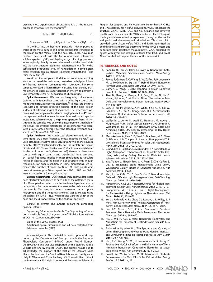
explains most experimental observations is that the reactionproceeds by a two-step mechanism:22
H2O2 þ 2Hþ f 2H2Oþ 2hþ (1)
Siþ nhþ þ 6HF f H2SiF6 þ nHþ þ 0:5(4 � n)H2v (2)
In the first step, the hydrogen peroxide is decomposed towater at the metal surface and in the process transfers holes tothe silicon via the metal. Next, the hole-rich silicon, now in anoxidized state, reacts with the hydrofluoric acid to form thesoluble species H2SiF6 and hydrogen gas. Etching proceedsanisotropically directly beneath the metal, and the metal sinksinto the nanostructure, resulting in a patternedmetal filmwith aself-aligned protruding array of nanopillars in a single step.Metal-assisted chemical etching is possible with both thin47 andthick metal films.42
We rinsed the samples with deionized water after etching.We then removed the resist using heated N-methyl pyrrolidoneand heated acetone, sometimes with sonication. For somesamples, we used a PlasmaTherm Versaline high-density plas-ma-enhanced chemical vapor deposition system to perform alow-temperature (90 �C) deposition of silicon nitride.
Optical Measurements. We used an integrating sphere setup(painted with Spectraflect paint) with a white light source andmonochromator, as reported elsewhere,10 to measure the total(specular and diffuse) reflection spectra of the gold�siliconsurfaces at different angles of incidence. The reflectance wasmeasured over angles of incidence ranging from 5 to 45� suchthat specular reflection from the sample would not escape theintegrating sphere through the sphere's aperture. Transmissionthrough the samples was below the measurement threshold ofthe setup. The average reflectance or absorptance was calcu-lated as a weighted average over the standard reference solarspectrum24 from 400 to 900 nm.
Optical Simulations. We conducted electromagnetic simula-tions using S4, a free frequency modal method solver.23 Weused standard refractive index values from two online sources,namely, http://refractiveindex.info/ for the metals and siliconnitride and http://www.filmetrics.com/refractive-index-database/for the semiconductors (Si, GaAs, and InP). We used a plane wavesource with equal parts s- and p-polarized light. We used24 spatial frequency modes in most simulations to calculatereflection spectra and the fields in our structure with enoughresolution. For finer resolution in some simulations, we in-creased the number of modes to 37 or 100. Data points weretaken at wavelengths 10 nm apart from 400 to 900 nm. Fieldswere extracted on a 5 nm grid spacing.
Electrical Measurements. Our structure included two large goldpads electrically connected to each side of the patterned metalfilm. We applied a conductive adhesive to each pad and used atwo-point probe measurement to measure the resistance (R) ofthe sample. The sample size was measured in an opticalmicroscope, and the sheet resistance (Rs) was calculated usingthe expression Rs = R�W/L, whereW and L are the width of thepads and the distance between the pads, respectively.
Conflict of Interest: The authors declare no competingfinancial interest.
Supporting Information Available: The Supporting Informa-tion is available free of charge on the ACS Publications websiteat DOI: 10.1021/acsnano.5b04034.
Video of the MACE process (AVI)Additional optical simulations and all data collected fromfabricated samples (PDF)
Acknowledgment. This material is based upon work sup-ported by the Department of Energy through the Bay AreaPhotovoltaic Consortium (BAPVC) under Award NumberDE-EE0004946 and was also supported by the Stanford GlobalClimate and Energy Project (GCEP). The authors would like toacknowledge the support of the staff at the Stanford NanoShared Facilities and the Stanford Nanofabrication Facility, espe-cially R. Tiberio and C. Knollenberg. V.K.N. would like to thankthe International Fulbright Science and Technology Fellowship
Program for support, and he would also like to thank P.-C. Hsuand I. Karakasoglu for helpful discussions. V.K.N. conceived thestructure. V.K.N., T.M.H., R.A.L., and Y.C. designed and reviewedresults from the experiments. V.K.N. conducted the etching, ARcoating, and characterization experiments, analyzed the results,and performed electromagnetic simulations. T.M.H. and R.A.L.provided some silicon wafers. V.K.N. and T.M.H. optimized thegold thickness and surface treatment for the MACE process andperformed sheet resistance measurements. V.K.N. prepared thefigures with layout and design assistance from R.A.L. and T.M.H.All authors helped prepare the text of the manuscript.
REFERENCES AND NOTES1. Kapadia, R.; Fan, Z.; Takei, K.; Javey, A. Nanopillar Photo-
voltaics: Materials, Processes, and Devices. Nano Energy2012, 1, 132–144.
2. Jeong, S.; Garnett, E. C.; Wang, S.; Yu, Z.; Fan, S.; Brongersma,M. L.; McGehee, M. D.; Cui, Y. Hybrid Silicon Nanocone-Polymer Solar Cells. Nano Lett. 2012, 12, 2971–2976.
3. Garnett, E.; Yang, P. Light Trapping in Silicon NanowireSolar Cells. Nano Lett. 2010, 10, 1082–1087.
4. Tian, B.; Zheng, X.; Kempa, T. J.; Fang, Y.; Yu, N.; Yu, G.;Huang, J.; Lieber, C. M. Coaxial Silicon Nanowires as SolarCells and Nanoelectronic Power Sources. Nature 2007,449, 885–889.
5. Cao, L.; Fan, P.; Vasudev, A. P.; White, J. S.; Yu, Z.; Cai, W.;Schuller, J. A.; Fan, S.; Brongersma, M. L. SemiconductorNanowire Optical Antenna Solar Absorbers. Nano Lett.2010, 10, 439–445.
6. Wallentin, J.; Anttu, N.; Asoli, D.; Huffman, M.; Aberg, I.;Magnusson, M. H.; Siefer, G.; Fuss-Kailuweit, P.; Dimroth, F.;Witzigmann, B.; et al. InP Nanowire Array Solar CellsAchieving 13.8% Efficiency by Exceeding the Ray OpticsLimit. Science 2013, 339, 1057–1060.
7. Mavrokefalos, A.; Han, S. E.; Yerci, S.; Branham, M. S.; Chen,G. Efficient Light Trapping in Inverted Nanopyramid ThinCrystalline Silicon Membranes for Solar Cell Applications.Nano Lett. 2012, 12, 2792–2796.
8. Grandidier, J.; Callahan, D. M.; Munday, J. N.; Atwater, H. A.Light Absorption Enhancement in Thin-Film Solar CellsUsing Whispering Gallery Modes in Dielectric Nano-spheres. Adv. Mater. 2011, 23, 1272–1276.
9. Yao, Y.; Yao, J.; Narasimhan, V. K.; Ruan, Z.; Xie, C.; Fan, S.;Cui, Y. Broadband Light Management Using Low-QWhispering Gallery Modes in Spherical Nanoshells. Nat.Commun. 2012, 3, 664.
10. Zhu, J.; Hsu, C.-M.; Yu, Z.; Fan, S.; Cui, Y. Nanodome SolarCells With Efficient Light Management and Self-Cleaning.Nano Lett. 2010, 10, 1979–1984.
11. Narasimhan, V. K.; Cui, Y. Nanostructures for Photon Man-agement in Solar Cells. Nanophotonics 2013, 2, 187–210.
12. Brongersma, M. L.; Cui, Y.; Fan, S. Light Managementfor Photovoltaics Using High-Index Nanostructures. Nat.Mater. 2014, 13, 451–460.
13. Ye, S.; Rathmell, A. R.; Chen, Z.; Stewart, I. E.; Wiley, B. J.Metal Nanowire Networks: The Next Generation of Trans-parent Conductors. Adv. Mater. 2014, 26, 6670–6687.
14. Lee, J.-Y.; Connor, S. T.; Cui, Y.; Peumans, P. Solution-Processed Metal Nanowire Mesh Transparent Electrodes.Nano Lett. 2008, 8, 689–692.
15. Hu, L.; Wu, H.; Cui, Y. Metal Nanogrids, Nanowires, andNanofibers for Transparent Electrodes.MRS Bull. 2011, 36,760–765.
16. Rathmell, A. R.; Wiley, B. J. The Synthesis and Coating ofLong, Thin Copper Nanowires to Make Flexible, Transpar-ent Conducting Films on Plastic Substrates. Adv. Mater.2011, 23, 4798–4803.
17. Hsu, P.-C.; Wang, S.; Wu, H.; Narasimhan, V. K.; Kong, D.;Ryoung Lee, H.; Cui, Y. Performance Enhancement ofMetalNanowire Transparent Conducting Electrodes by Meso-scale Metal Wires. Nat. Commun. 2013, 4, 2522.
18. Rowell, M. W.; McGehee, M. D. Transparent ElectrodeRequirements for Thin Film Solar Cell Modules. EnergyEnviron. Sci. 2011, 4, 131.
ARTIC
LE

NARASIMHAN ET AL. VOL. XXX ’ NO. XX ’ 000–000 ’ XXXX
www.acsnano.org
H
19. Spinelli, P.; Verschuuren, M. A.; Polman, A. BroadbandOmnidirectional Antireflection Coating Based on Sub-wavelength Surface Mie Resonators. Nat. Commun.2012, 3, 692.
20. Wang, K. X.; Yu, Z.; Sandhu, S.; Liu, V.; Fan, S. Condition forPerfect Antireflection by Optical Resonance at MaterialInterface. Optica 2014, 1, 388.
21. Yu, Y.; Cao, L. Leaky Mode Engineering: A General DesignPrinciple for Dielectric Optical Antenna Solar Absorbers.Opt. Commun. 2014, 314, 79–85.
22. Chartier, C.; Bastide, S.; Lévy-Clément, C. Metal-AssistedChemical Etching of Silicon in HF�H2O2. Electrochim. Acta2008, 53, 5509–5516.
23. Liu, V.; Fan, S. S4: A Free Electromagnetic Solver forLayered Periodic Structures. Comput. Phys. Commun.2012, 183, 2233–2244.
24. International ASTM. ASTM G173�03(2012), StandardTables for Reference Solar Spectral Irradiances: DirectNormal and Hemispherical on 37� Tilted Surface; WestConshohocken, PA, 2012.
25. Tous, L.; Russell, R.; Debucquoy, M.; Posthuma, N.;Duerinckx, F.; Mertens, R.; Poortmans, J. Power-LossAnalysis of Advanced PERC Cells Reaching 20.5%Energy Conversion Efficiency. Energy Procedia 2013, 38,467–473.
26. Ellmer, K. Past Achievements and Future Challenges in theDevelopment of Optically Transparent Electrodes. Nat.Photonics 2012, 6, 809–817.
27. Ryan, C. G. M.; Eleftheriades, G. V. Single- and Dual-BandTransparent Circularly Polarized Patch Antennas WithMetamaterial Loading. IEEE Antennas Wirel. Propag. Lett.2015, 14, 470–473.
28. Transparent Electronics; Facchetti, A., Marks, T. J., Eds.; JohnWiley & Sons, Ltd.: Chichester, UK, 2010.
29. Yang, Y.; Jeong, S.; Hu, L.; Wu, H.; Lee, S. W.; Cui, Y.Transparent Lithium-Ion Batteries. Proc. Natl. Acad. Sci. U.S. A. 2011, 108, 13013–13018.
30. Ebbesen, T. W.; Lezec, H. J.; Ghaemi, H. F.; Thio, T.; Wolff,P. A. Extraordinary Optical Transmission through Sub-Wavelength Hole Arrays. Nature 1998, 391, 667–669.
31. Martín-Moreno, L.; García-Vidal, F.; Lezec, H.; Pellerin, K.;Thio, T.; Pendry, J.; Ebbesen, T. Theory of ExtraordinaryOptical Transmission through Subwavelength Hole Arrays.Phys. Rev. Lett. 2001, 86, 1114–1117.
32. Genet, C.; Ebbesen, T. W. Light in Tiny Holes. Nature 2007,445, 39–46.
33. Koerkamp, K. J. K.; Enoch, S.; Segerink, F. B.; van Hulst, N. F.;Kuipers, L. Strong Influence of Hole Shape on Extraordi-nary Transmission through Periodic Arrays of Subwave-length Holes. Phys. Rev. Lett. 2004, 92, 183901.
34. Van derMolen, K. L.; Segerink, F. B.; van Hulst, N. F.; Kuipers,L. Influence of Hole Size on the Extraordinary Transmissionthrough Subwavelength Hole Arrays. Appl. Phys. Lett.2004, 85, 4316.
35. Van der Molen, K. L.; Klein Koerkamp, K. J.; Enoch, S.;Segerink, F. B.; van Hulst, N. F.; Kuipers, L. Role of Shapeand Localized Resonances in Extraordinary Transmissionthrough Periodic Arrays of Subwavelength Holes: Experi-ment and Theory. Phys. Rev. B: Condens. Matter Mater.Phys. 2005, 72, 045421.
36. Yokogawa, S.; Burgos, S. P.; Atwater, H. A. Plasmonic ColorFilters for CMOS Image Sensor Applications. Nano Lett.2012, 12, 4349–4354.
37. Zeng, B.; Gao, Y.; Bartoli, F. J. Ultrathin NanostructuredMetals for Highly Transmissive Plasmonic SubtractiveColor Filters. Sci. Rep. 2013, 3, 2840.
38. Li, L.; Zhao, X.; Wong, C.-P. Deep Etching of Single- andPolycrystalline Silicon with High Speed, High Aspect Ratio,High Uniformity, and 3D Complexity by Electric Bias-Attenuated Metal-Assisted Chemical Etching (EMaCE).ACS Appl. Mater. Interfaces 2014, 6, 16782–16791.
39. DeJarld, M.; Shin, J. C.; Chern, W.; Chanda, D.; Balasundaram,K.; Rogers, J. A.; Li, X. Formation of High Aspect Ratio GaAsNanostructures with Metal-Assisted Chemical Etching.Nano Lett. 2011, 11, 5259–5263.
40. Dimova-Malinovska, D.; Sendova-Vassileva, M.; Tzenov,N. U.; Kamenova, M. Preparation of Thin Porous SiliconLayers by Stain Etching. Thin Solid Films 1997, 297, 9–12.
41. Yae, S.; Morii, Y.; Fukumuro, N.; Matsuda, H. CatalyticActivity of Noble Metals for Metal-Assisted ChemicalEtching of Silicon. Nanoscale Res. Lett. 2012, 7, 352.
42. Chang, C.; Sakdinawat, A. Ultra-High Aspect Ratio High-Resolution Nanofabrication for Hard X-Ray DiffractiveOptics. Nat. Commun. 2014, 5, 4243.
43. Mikhael, B.; Elise, B.; Xavier, M.; Sebastian, S.; Johann, M.;Laetitia, P. New Silicon Architectures by Gold-AssistedChemical Etching. ACS Appl. Mater. Interfaces 2011, 3,3866–3873.
44. Liu, R.; Zhang, F.; Con, C.; Cui, B.; Sun, B. Lithography-FreeFabrication of Silicon Nanowire and Nanohole Arrays byMetal-Assisted Chemical Etching. Nanoscale Res. Lett.2013, 8, 155.
45. Bielawny, A.; Upping, J.; Miclea, P. T.; Wehrspohn, R. B.;Rockstuhl, C.; Lederer, F.; Peters, M.; Steidl, L.; Zentel, R.;Lee, S.-M.; et al. 3D Photonic Crystal IntermediateReflector for Micromorph Thin-Film Tandem Solar Cell.Phys. Status Solidi A 2008, 205, 2796–2810.
46. Zhen, A.; Ma, P.; Zhang, Y.; Guo, E.; Tian, Y.; Liu, B.; Guo, S.;Shan, L.; Wang, J.; Li, J. Embeded Photonic Crystal at theInterface of P-GaN and Ag Reflector to Improve LightExtraction of GaN-Based Flip-Chip Light-Emitting Diode.Appl. Phys. Lett. 2014, 105, 251103.
47. Li, L.; Liu, Y.; Zhao, X.; Lin, Z.; Wong, C.-P. Uniform VerticalTrench Etching on SiliconwithHighAspect Ratio byMetal-Assisted Chemical Etching Using Nanoporous Catalysts.ACS Appl. Mater. Interfaces 2014, 6, 575–584.
ARTIC
LE