ht7a6312 low power primary switcher for off line smps · rev. 1.30 3 january 18, 2018 ht7a6312...
TRANSCRIPT
Rev. 1.30 1 January 18, 2018 Rev. 1.00 PB January 18, 2018
HT7A6312Low Power Primary Switcher for Off Line SMPS
Features• Fixed60kHzswitchingfrequency• 9Vto38VwiderangeVCCvoltage• WideACinputrangefrom85VACto265VAC
• PWMwithcurrentmodecontrol• AuxiliaryUnderVoltageLockOutwithhysteresis• Highvoltagestart-upcurrentsource• Excellentstandbylowpowerconsumption• Over-temperature,Over-currentandOver-voltageprotectionwithauto-restart
• Integrated730VMOSFET• Burstmodeunderlowloadconditions
Applications• Offlinepowersupplyforbatterychargeradapters• StandbypowersupplyforTVormonitors• Auxiliarysupplyformotorcontrol• Airconditionerpowersupply• Electromagneticovenpowersupply
General DescriptionTheHT7A6312 is highly functionally integrateddevicewhichcombinesanintegratedPWMcontrollerwithcurrentmodecontrolandahighvoltagepowerMOSFETonthesamesiliconchip.
Typical Power CapabilityType 8SOP 8DIP
European (195~265VAC) 8W 13WUS (85~265VAC) 5W 8W
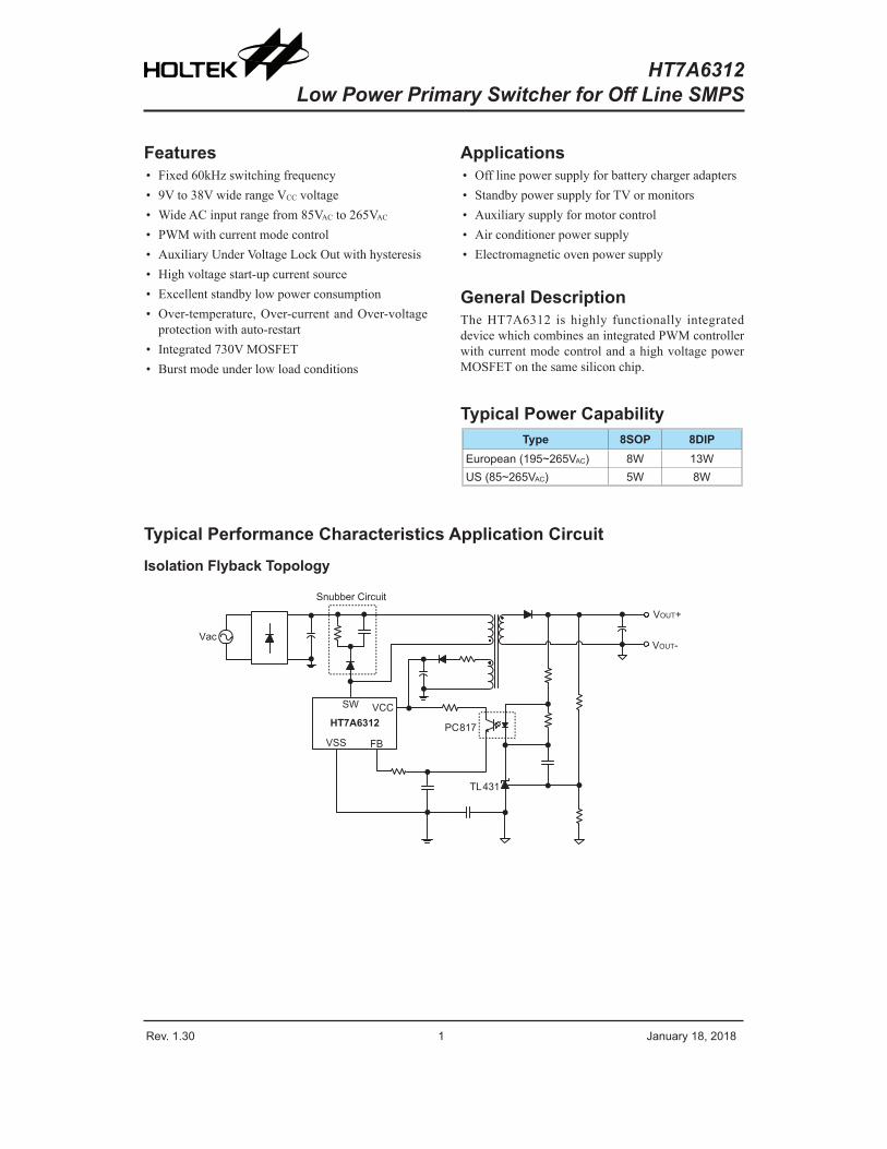
Typical Performance Characteristics Application Circuit
Isolation Flyback Topology
VOUT+
VOUT-
PC817
TL431
HT7A6312
VSS
SW
FB
VCC
Vac
Snubber Circuit
Rev. 1.30 2 January 18, 2018
HT7A6312
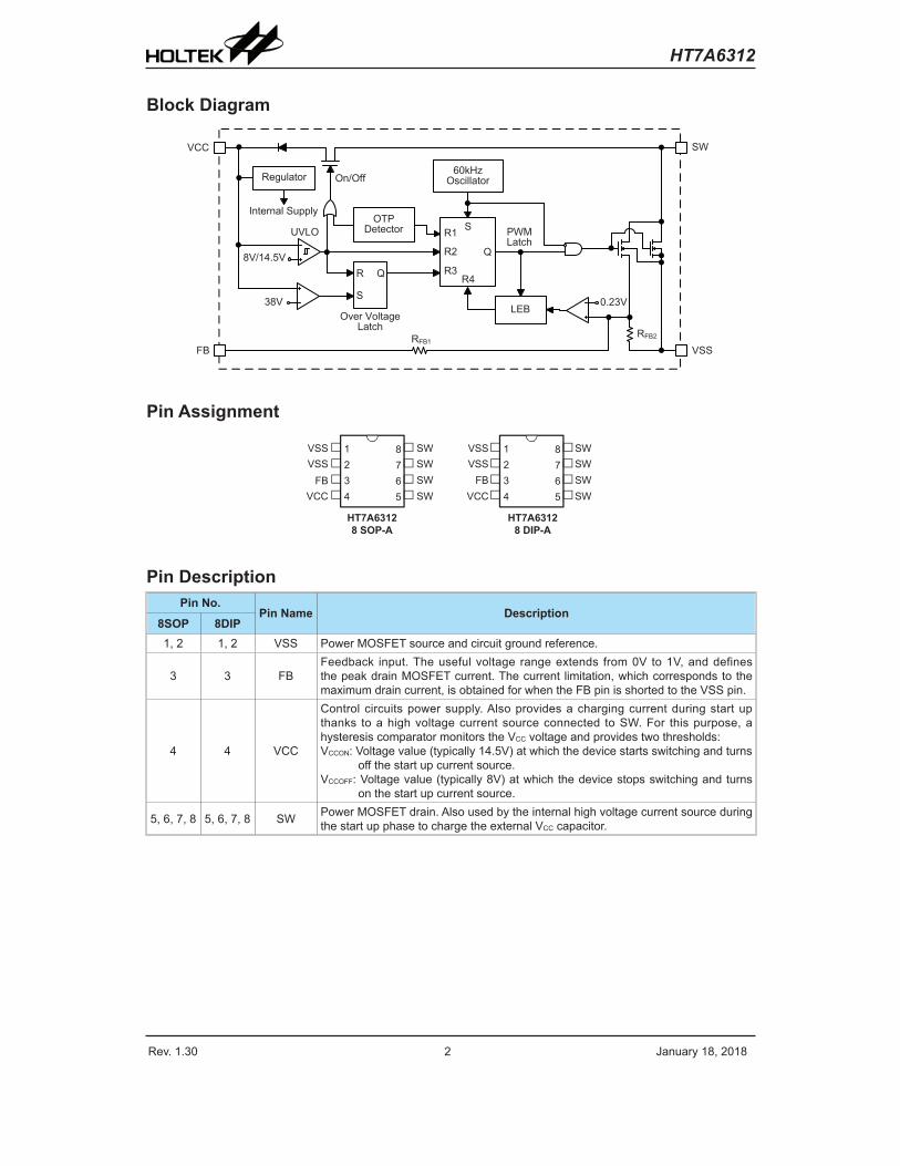
Block Diagram
60kHzOscillator
OTPDetector
LEB
Regulator
UVLO
8V/14.5V
38V 0.23V
R1
R2
R3
S
R4
Q
R
S
Q
On/Off
RFB1
Internal Supply
Over VoltageLatch
PWMLatch
VCC
FB
SW
VSSRFB2
Pin Assignment
VSSSW
FB
VSS
SWSWSW
VCC
HT7A63128 SOP-A
VSSSW
FB
VSS
SWSWSW
VCC
1234
8765
1234
8765
HT7A63128 DIP-A
Pin DescriptionPin No.
Pin Name Description8SOP 8DIP1, 2 1, 2 VSS Power MOSFET source and circuit ground reference.
3 3 FBFeedback input. The useful voltage range extends from 0V to 1V, and defines the peak drain MOSFET current. The current limitation, which corresponds to the maximum drain current, is obtained for when the FB pin is shorted to the VSS pin.
4 4 VCC
Control circuits power supply. Also provides a charging current during start up thanks to a high voltage current source connected to SW. For this purpose, a hysteresis comparator monitors the VCC voltage and provides two thresholds:VCCON: Voltage value (typically 14.5V) at which the device starts switching and turns
off the start up current source.VCCOFF: Voltage value (typically 8V) at which the device stops switching and turns
on the start up current source.
5, 6, 7, 8 5, 6, 7, 8 SW Power MOSFET drain. Also used by the internal high voltage current source during the start up phase to charge the external VCC capacitor.
Rev. 1.30 3 January 18, 2018
HT7A6312
Absolute Maximum Ratings Symbol Parameter Value Unit
VDS(sw) Switching Drain Source Voltage (TJ=25 to 125°C)(1) -0.3 to 730 VVDS(st) Start-up Drain Source Voltage (TJ=25 to 125°C)(2) -0.3 to 400 VID Continuous Drain Current Internally limited AVCC Supply Voltage 0 to 41 VIFB Feedback Current 3 mA
VESDElectrostatic Discharge: Machine mode 400 VElectrostatic Discharge: Human body mode 3 kV
TC Operating Temperature Range -40 to 150 °CTSTG Storage Temperature Range -55 to 150 °CTJ Junction Operating Temperature Internally limited °C
Note:1.Thisparameterapplieswhenthestart-upcurrentsourceisoff.ThisisthecasewhentheVCCvoltagehasreachedVCCONandremainsaboveVCCOFF.
2.Thisparameterapplieswhenthestartupcurrentsourceison.ThisisthecasewhentheVCCvoltagehasnotyetreachedVCCONorhasfallenbelowVCCOFF.
Thermal Data
Symbol Parameter 8SOP 8DIP UnitRTHJC Thermal resistance junction-case 25 15 °C/WRTHJA Thermal resistance ambient-case(Note) 55 45 °C/W
Note:Whenmountedonastandardsingle-sidedFR4boardwith200mm2ofCu(atleast35μmthick)connectedtoallSWpins.
Rev. 1.30 4 January 18, 2018
HT7A6312
Electrical CharacteristicsTa=25°C, VCC=18V, unless otherwise specified
Symbol Parameter Test Conditions Min. Typ. Max. UnitPower SectionBVDSS Drain-Source Voltage ID=1mA; VFB=2V 730 — — VIDSS Off State Drain Current VDS=500V; VFB=2V; TJ=125°C — — 0.1 mArDS(ON) Static Drain-Source On State Resistance ID=0.2A — 19 22 ΩtF Fall Time ID=0.1A; VIN=300V(1) — 100 — nStR Rise Time ID=0.2A; VIN=300V(1) — 50 — nSCOSS Drain Capacitance VDS=25V — 20 — pFSupply SectionICCCH Start-Up Charging Current VDS=100V; VCC=0V to VCCON — -1 — mA
ICCOFFStart-Up Charging Current In Thermal Shutdown
VCC=5V; VDS=100V TJ > TSD - THYST
0 — — mA
ICCOperating Supply Current Not Switching IFB=2mA — 0.65 0.8 mAOperating Supply Current Switching IFB=0.5mA; ID=50mA(2) — 0.7 0.9 mA
DRST Restart Duty-Cycle — — 16 — %VCCOFF VCC Under-voltage Shutdown Threshold — 7 8 9 VVCCON VCC Start-Up Threshold — 13 14.5 16 VVCCHYST VCC Threshold Hysteresis — 5.8 6.5 7.2 VVCCOVP VCC Over-voltage Threshold — 35 38 41 VOscillation SectionfOSC Oscillator Frequency Total Variation VCC=VCCOFF to 35V; TJ=0 to 100°C 54 60 66 kHzPWM Comparator SectionGID IFB to ID Current Gain — — 320 — —IDLIM Peak Current Limitation VFB=0V 0.32 0.4 0.48 AIFBSD IFB Shutdown Current — — 0.9 — mARFB FB Pin Input Impedance ID=0mA — 1.2 — kΩtD Current Sense Delay to Turn-Off ID=0.2A — 200 — nStB Blanking Time — — 350 — nStONMIN Minimum Turn-On Time — — 550 — nSOver-temperature SectionTSD Thermal Shutdown Temperature — 140 170 — °CTHYST Thermal Shutdown Hysteresis — — 40 — °C
Note:Absolutemaximumratingsindicatelimitsbeyondwhichdamagetothedevicemayoccur.OperatingRatingsindicateconditionsforwhichthedeviceisintendedtobefunctional,butdonotguaranteespecificperfor-mancelimits.Theguaranteedspecificationsapplyonlyforthetestconditionslisted.
1.Forclampedinductiveload
2.Thesetestconditionsareobtainedwitharesistiveloadwhichpermitthemaximumconductiontimeofthedevice.
Rev. 1.30 5 January 18, 2018
HT7A6312
Functional DescriptionTheHT7A6312 is highly functionally integrateddevicewhichcombinesanintegratedPWMcontrollerwithcurrentmodecontrolandahighvoltagepowerMOSFETon thesamesiliconchip.Thesecondarysidefeedbacksignalpassesthroughaphoto-coupleron the primary sidewhile the output voltage isregulatedby thedeviceaccording to the feedbacksignal.Thedevice has a small quiescent currentand low power consumptionwhen operating inthestandbymode. Italsohasa rangeofprotectionfeaturestoprotectthecontrollerfromfaultconditions.
High Voltage Start upTheSWpin in thedevice isahighvoltagestartupcurrent source.Thiscurrent sourcewillgenerateacurrentwhich is regulatedfromahighvoltageandwhichwill charge theVCCpin until theUVLOis triggeredwhenanACvoltage isappliedon theconverter input.WhentheVCCvoltageis largerthantheUVLOtriggervoltage, thehighvoltagestartupcurrentsourcewillbecutoffbyUVLOandthedevicewillstartoperationbyswitchingthepowerMOSFETonandoff.
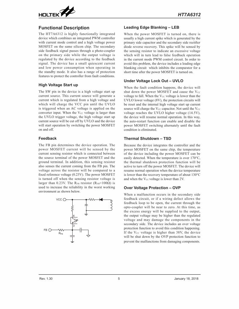
FeedbackTheFBpindetermines thedeviceoperation.ThepowerMOSFET currentwill be sensed by thecurrentsensingresistorwhichisconnectedbetweenthesource terminalof thepowerMOSFETand theground terminal. Inaddition, this sensing resistoralsosensesthecurrentcomingfromtheFBpin.Thevoltage across the resistorwill be compared to afixedreferencevoltage(0.23V).ThepowerMOSFETis turnedoffwhen the sensing resistorvoltage islarger than0.23V.TheRFB resistor (RFB=100Ω) isusedto increasethereliability in theworstworkingenvironmentasshownbelow.
VCC
FB3
4
RFB
Leading Edge Blanking – LEBWhen thepowerMOSFET is turnedon, there isusuallyahighcurrentspikewhichisgeneratedbytheprimarysidecapacitorandthesecondarysiderectifierdiodereverserecovery.Thisspikewillbesensedbythesensingresistor to indicateanexcessivevoltagewhichwill in turn lead to false feedbackoperationinthecurrentmodePWMcontrolcircuit.Inordertoavoidthisproblem,thedeviceincludesaleadingedgeblankingcircuit whichinhibits thecomparatorforashorttimeafterthepowerMOSFETisturnedon.
Under Voltage Lock Out – UVLOWhen the faultconditionhappens, thedevicewillshutdown thepowerMOSFETandcause theVCCvoltagetofall.WhentheVCCvoltageislowerthantheUVLOlowervoltage(8V),theprotectioncircuitswillberesetandtheinternalhighvoltagestartupcurrentsourcewillchargetheVCCcapacitor.NotuntiltheVCCvoltagereaches theUVLOhighervoltage(14.5V),thedevicewillresumenormaloperation.Inthisway,theauto-restart functioncanenableanddisable thepowerMOSFETswitchingalternatelyuntil thefaultconditioniseliminated.
Thermal Shutdown – TSDBecause thedevice integrates thecontrollerandthepowerMOSFETon thesamechip, the temperatureof thedevice includingthepowerMOSFETcanbeeasilydetected.Whenthetemperatureisover170°C,the thermal shutdownprotection functionwill beactivetoturnoffthepowerMOSFET.Thedevicewillresumenormaloperationwhenthedevicetemperatureislowerthantherecoverytemperatureofabout130°CandwhentheVCCvoltageislowerthan2V.
Over Voltage Protection – OVPWhenamalfunctionoccurs in the secondary sidefeedbackcircuit, or if awiringdefect allows thefeedback loop tobeopen, thecurrent through theopto-couplerwillbenear tozero.At this time,asthe excess energywill be supplied to theoutput,theoutputvoltagemaybehigher thantheregulatedvoltage andmay damage the components in thesecondaryside.Thedeviceincludesanovervoltageprotectionfunctiontoavoidthisconditionhappening.If theVCC voltage ishigher than38V, thedevicewillbeshutdownbytheOVPprotectionfunctiontopreventthemalfunctionsfromdamagingcomponents.
Rev. 1.30 6 January 18, 2018
HT7A6312
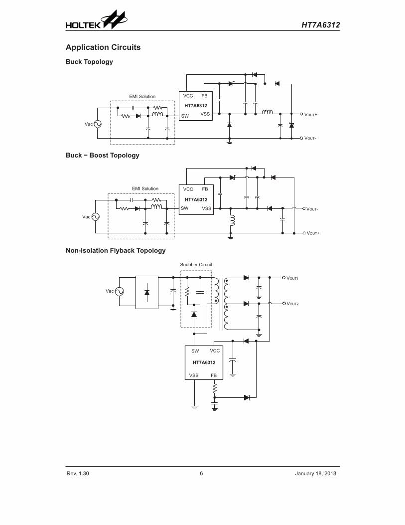
Application Circuits
Buck Topology
VSSSW
VCC FBEMI Solution
HT7A6312
VOUT-
Vac
VOUT+
Buck − Boost Topology
EMI Solution
VSSSW
VCC FB
HT7A6312
VOUT+
VOUT-
Vac
Non-Isolation Flyback Topology
HT7A6312
FBVSS
SW VCC
Snubber Circuit
VOUT1
VOUT2
Vac
Rev. 1.30 7 January 18, 2018
HT7A6312
Package Information
Notethat thepackageinformationprovidedhereisforconsultationpurposesonly.Asthis informationmaybeupdatedatregularintervalsusersareremindedtoconsulttheHoltekwebsiteforthelatestversionofthePackage/CartonInformation.
Additionalsupplementaryinformationwithregardtopackagingislistedbelow.Clickontherelevantsectiontobetransferredtotherelevantwebsitepage.
• PackageInformation(includeOutlineDimensions,ProductTapeandReelSpecifications)
• TheOperationInstructionofPackingMaterials
• Cartoninformation
Rev. 1.30 8 January 18, 2018
HT7A6312
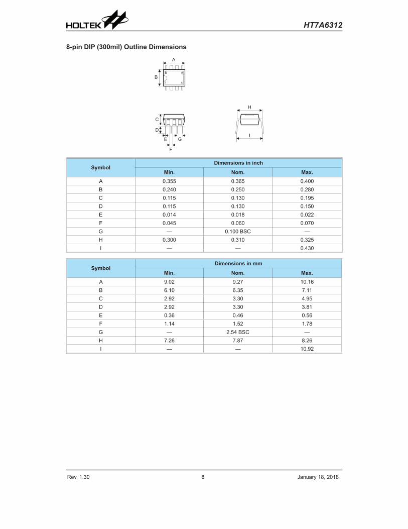
8-pin DIP (300mil) Outline Dimensions
� �� �
��
�
�
�
�
�
�
�
�
�
SymbolDimensions in inch
Min. Nom. Max.A 0.355 0.365 0.400B 0.240 0.250 0.280C 0.115 0.130 0.195 D 0.115 0.130 0.150 E 0.014 0.018 0.022 F 0.045 0.060 0.070G — 0.100 BSC —H 0.300 0.310 0.325 I — — 0.430
SymbolDimensions in mm
Min. Nom. Max.A 9.02 9.27 10.16 B 6.10 6.35 7.11 C 2.92 3.30 4.95 D 2.92 3.30 3.81 E 0.36 0.46 0.56 F 1.14 1.52 1.78G — 2.54 BSC —H 7.26 7.87 8.26I — — 10.92
Rev. 1.30 9 January 18, 2018
HT7A6312
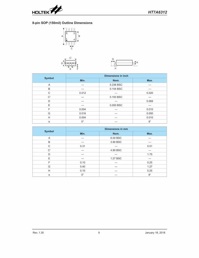
8-pin SOP (150mil) Outline Dimensions
�
�
� � ��
��
�
�� �
�
�
�
SymbolDimensions in inch
Min. Nom. Max.A — 0.236 BSC —B — 0.154 BSC —C 0.012 — 0.020C′ — 0.193 BSC —D — — 0.069E — 0.050 BSC —F 0.004 — 0.010G 0.016 — 0.050H 0.004 — 0.010α 0° — 8°
SymbolDimensions in mm
Min. Nom. Max.A — 6.00 BSC —B — 3.90 BSC —C 0.31 — 0.51C′ — 4.90 BSC —D — — 1.75E — 1.27 BSC —F 0.10 — 0.25G 0.40 — 1.27H 0.10 — 0.25α 0° — 8°
Rev. 1.30 10 January 18, 2018
HT7A6312
Copyright© 2018 by HOLTEK SEMICONDUCTOR INC.
The information appearing in this Data Sheet is believed to be accurate at the time of publication. However, Holtek assumes no responsibility arising from the use of the specifications described. The applications mentioned herein are used solely for the purpose of illustration and Holtek makes no warranty or representation that such applications will be suitable without further modification, nor recommends the use of its products for application that may present a risk to human life due to malfunction or otherwise. Holtek's products are not authorized for use as critical components in life support devices or systems. Holtek reserves the right to alter its products without prior notification. For the most up-to-date information, please visit our web site at http://www.holtek.com.tw.