ht16k33 ram mapping 16×8 led controller driver with keyscan · ram mapping 16×8 led controller...
TRANSCRIPT

Rev. 1.20 1 July 12, 2017 Rev. 1.00 PB July 12, 2017
HT16K33RAM Mapping 16×8 LED
Controller Driver with Keyscan
Feature• Operatingvoltage:4.5V~5.5V• IntegratedRCoscillator• I2C-businterface• 16×8bitsRAMfordisplaydatastorage• Max.16×8patterns,16segmentsand8commons• R/Waddressautoincrement• Max.13×3matrixkeyscanning• 16-stepdimmingcircuit• Selectionof20/24/28-pinSOPpackagetypes
Applications• Industrialcontrolindicators• Digitalclocks,thermometers,counters,multimeters• Combosets
• VCRsets• Instrumentationreadouts• Otherconsumerapplications• LEDDisplays
General DescriptionTheHT16K33 is amemorymapping andmulti-functionLEDcontrollerdriver.Themax.Displaysegmentnumbers in thedevice is128patterns (16segments and 8 commons)with a 13×3 (MAX.)matrixkeyscancircuit.Thesoftwareconfigurationfeatures of theHT16K33makes it suitable formultipleLEDapplications includingLEDmodulesanddisplaysubsystems.TheHT16K33iscompatiblewithmostmicrocontrollersandcommunicatesviaatwo-linebidirectionalI2C-bus.
Block Diagram
Row driver outputInterrupt function output
Key data inputDevice address data
input
DisplayRAM
16×8bits
Timinggenerator
I2 CC
ontro
ller
COM0/AD
COM1/KS0
COM2/KS1
COM3/KS2
ROW0/A2
VDD
VSS
SDA
SCL
Power_on reset COM5
COM6
COM7
COM4
POR
POR
ROW1/A1
ROW12/K10
ROW15/K13/INT
Key data RAM
13×3bits
POR
ROW13/K11
ROW14/K12
ROW2/A0
ROW3/K1
InternalRC
Oscillator
Common scan outputKey scan outputDevice address source output
A[2:0]
POR
POR
POR
POR

Rev. 1.20 2 July 12, 2017
HT16K33
Pin Assignment

Rev. 1.20 3 July 12, 2017
HT16K33
Pin DescriptionPin Name Type Description
SDA I/O I2C interface Serial Data Input/OutputSCL I I2C interface Serial Clock InputVDD — Positive power supply for logic circuitVSS — Negative power supply for logic circuit, ground
COM0/AD O•Common output pin, active low during display•Also used as device address source output pin, active high during power on reset
and key scan
COM1/KS0~COM3/KS2 O •Common output pin, active low when displaying•Also used as the Key source output pin, active high during key scan operation
COM4~COM7 O Common outputs pin, active low during display.28 Pin package
ROW0/A2~ROW2/A0 I/O•ROW output pin, active high when displaying•Also used as the device address data input pin, internal pull-low during power on
reset and during key scan operation
ROW3/K1~ROW14/K12 I/O •ROW outputs pin, active high during display.•Also used as the Key data input pin, internal pull-low during key scan operation
ROW15/K13 /INT I/O
•When the “INT/ROW” bit of ROW/INT set register is set to “0”, this pin become a Row driver output pin, active high when displaying, and Key data input during key scan operation.
•When the “INT/ROW” bit of ROW/INT set register is set to “1”, this pin become Interrupt signal (INT) output pin.
•INT pin output active-high when the “act” bit of the Row/int setup register is set to “0”.•INT pin output active-high when the “act” bit of the ROW/INT register is set to “1”.
24 Pin package
ROW0/A1~ROW1/A0 I/O•ROW output pin, active high when displaying•Also used as the device address data input pin, internal pull-low during a power on
reset and during a key scan operation
ROW2/K1~ROW10/K9 I/O •ROW outputs pin, active high when displaying•Also used as the Key data inputs pin, internal pull-low during a key scan operation
ROW11/K10/INT I/O
•When the “INT/ROW” bit of ROW/INT set register is set to “0”, this pin become a Row driver output, active high when displaying, and Key data input during a keyscan operation
•When the “INT/ROW” bit of ROW/INT set register is set to “1”, this pin become an Interrupt signal (INT) output pin.
•INT pin output active-high when the “act” bit of the Row/int setup register is set to “0”.•INT pin output active-high when the “act” bit of the Row/int setup register is set to “1”.
20 Pin package
ROW0/K1~ROW6/K7 I/O •ROW output pin, active high when displaying•Also used as the Key data inputs pin, internal pull-low during a key scan operation
ROW7/K8 /INT I/O
•When the “INT/ROW” bit of the ROW/INT setup register is set to “0”, this pin become a Row driver output, active high when displaying, and Key data input during a key scan operation
•When the “INT/ROW” bit of the ROW/INT set register is set to “1”, this pin become an Interrupt (INT) signal output pin
•INT pin output active-high when the “act” bit of ROW/INT setup register is set to “0” •INT pin output active-high when the “act” bit of the ROW/INT set register is set to “1”
Rev. 1.20 4 July 12, 2017
HT16K33
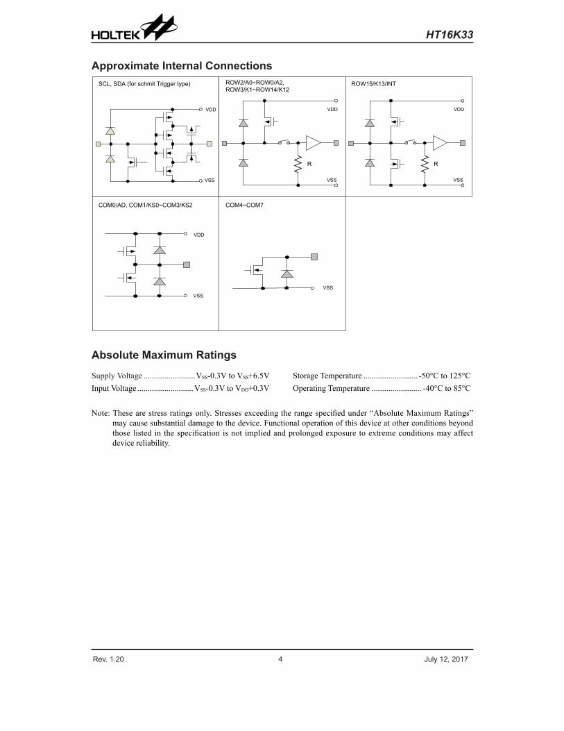
Approximate Internal ConnectionsSCL, SDA (for schmit Trigger type) ROW2/A0~ROW0/A2,
ROW3/K1~ROW14/K12
COM0/AD, COM1/KS0~COM3/KS2
VSS
VDD
COM4~COM7
ROW15/K13/INT
VDD
VSS
R
VSS
VDD
VSS
VDD
R
VSS
Absolute Maximum Ratings
SupplyVoltage.........................VSS-0.3VtoVSS+6.5VInputVoltage...........................VSS-0.3VtoVDD+0.3V
StorageTemperature.......................... -50°Cto125°COperatingTemperature........................ -40°Cto85°C
Note:Thesearestressratingsonly.Stressesexceedingtherangespecifiedunder“AbsoluteMaximumRatings”maycausesubstantialdamagetothedevice.Functionaloperationofthisdeviceatotherconditionsbeyondthoselistedin thespecificationisnot impliedandprolongedexposuretoextremeconditionsmayaffectdevicereliability.

Rev. 1.20 5 July 12, 2017
HT16K33
D.C. CharacteristicsVDD=4.5~5.5V;Ta=25°C(Unlessotherwisespecified)
Symbol ParameterTest Conditions
Min. Typ. Max. UnitVDD Conditions
VDD Operating Voltage — — 4.5 5 5.5 V
IDD Operating Current 5 No load, normal operation, INT/ROW bit is set to “0” — 1 2 mA
ISTB Standby Current 5 No load, standby mode — 1 10 μAVIH Input high Voltage 5 SDA, SCL 0.7VDD — VDD VVIL Input Low Voltage 5 SDA, SCL 0 — 0.3VDD VIIL Input leakage current — VIN=VSS or VDD -1 — 1 μA
RPL Input pull-low resistor 5 ROW3/K1~ROW15/K13,ROW0/A2~ROW2/A0 Keyscan during 250 — — kΩ
IOL1 Low level output current 5 VOL=0.4V; SDA 6 — — mAIOL2 ROW Sink Current 5 VOL=0.4V, INT pin 6 — — mA
IOH1 ROW Source Current 5VOH=VDD-2V, (ROW0~ROW15 pin) -20 -25 -40 mAVOH=VDD-3V, (ROW0~ROW15 pin) -25 -30 -50 mA
Imath ROW Source Current tolerance 5 VOH=VDD-3V, (ROW0~ROW15 pin) — — 5 %IOL3 COM Sink Current 5 VOL=0.3V, (COM0~COM7 pin) 160 200 — mAIOH2 COM Source Current 5 VOH=VDD-2V, (COM0~COM3 pin) -20 -25 -40 mA
A.C. CharacteristicsVDD=4.5~5.5V;Ta=25°C(Unlessotherwisespecified)
Symbol ParameterTest Condition
Min. Typ. Max. UnitVDD Condition
tLED LED Frame time 5 1/9 Duty 7.6 9.5 11.4 mstOFF VDD OFF Time — VDD drop down to 0V 20 — — mstSR VDD Slew Rate — — 0.05 — — V/ms
Note:1.If thePoweronResettimingconditionsarenotsatisfiedinthepowerON/OFFsequence, theinternalPoweronResetcircuitwillnotoperatenormally.
2.IfVDDdropsbelowtheminimumvoltageoftheoperatingvoltagespec.duringoperating,thePoweronResettimingconditionsmustalsobesatisfied.Thatis,VDDmustdropto0Vandremainat0Vfor20ms(min.)beforerisingtothenormaloperatingvoltage.

Rev. 1.20 6 July 12, 2017
HT16K33
I2C Interface Electrical CharacteristicsSymbol Parameter Test Condition Min. Max. UnitfSCL Clock frequency — — 400 kHz
tBUF Bus free time Time in which the bus must be free before a new transmission can start 1.3 — μs
tHD:STA Start condition hold time After this period, the first clock pulse is generated 0.6 — μstLOW SCL Low time — 1.3 — μstHIGH SCL High time — 0.6 — μstSU:STA Start condition set-up time Only relevant for repeated START condition 0.6 — μstHD:DAT Data hold time — 0 — μstSU:DAT Data set-up time — 100 — nstr Rise time Note — 0.3 μstf Fall time Note — 0.3 μstSU:STO Stop condition set-up time — 0.6 — μstAA Output Valid from Clock — — 0.9 μs
tSPInput Filter Time Constant(SDA and SCL Pins) Noise suppression time — 50 ns
Note: These parameters are periodically sampled but not 100% tested.
Timing DiagramsI2C Timing
SDA
SCL
tf
tHD:SDA
tLOW tr
tHD:DAT
tSU:DAT
tHIGH tSU:STA
tHD:STA
S Sr
tSP
tSU:STO
P
tBUF
StAA
SDAOUT
Power-on Reset Timing
Rev. 1.20 7 July 12, 2017
HT16K33
Functional Description
Power-on ResetWhenpower isapplied, the IC is initialisedbyaninternal power-on reset circuit.The statusof theinternalcircuitafterinitialisationisasfollows:
• SystemOscillatorwillbeinanoffstate• COM0~COM3outputsaresettoVDD
• COM4~COM7outputswillbehighimpedance• AllRowspinsarechangedinputpins• LEDDisplayisintheoffstate.• Keyscanstopped• ThecombinedRow/INTpinsaresetupasROWoutputs
• Dimmingissetto16/16dutyDatatransfersontheI2C-busshouldbeavoidedfor1msfollowingapower-ontoallowcompletionoftheresetaction.
Standby ModeIn thestandbymode, theHT16K33cannotacceptinputcommandsnorwritedata to thedisplayRAMexceptusingthesystemsetupcommand.
If thestandbymode isselectedwith the“S”bitofthesystemsetupregistersetto“0”,thestatusofthestandbymodelisasfollows:
• SystemOscillatorwillbeintheoffstate• COM0~COM3outputsaresettoVDD• COM4~COM7outputswillbehighimpedance
• LEDDisplayisintheoffstate.• Keyscanstopped• Allkeydataand INTflagsarecleareduntil thestandbymodeiscanceled.
• Ifthekeymatrixisactivated(anykey)orthe“S”bitof thesystemsetupregister isset to“1”, thestandbymodewillbecanceledandwillcausethedevicetowake-up.
• If the “INT/ROW”bit of theROW/INT setupregisterisset to“0”,allrowspinsarechangedtoinputpins.
• If the “INT/ROW”bit of theROW/INT setupregisterissetto“1”:allrowspinsarechangedtoinputpinsexceptfortheINTpin(output).
• The INTpinoutputwill remainat ahigh levelwhenthe“act”bitoftheROW/INTsetupregisterissetto“0”.
• TheINTpinoutput remainsata lowlevelwhenthe“act”bitoftheROW/INTsetupregisterissetto“1”.
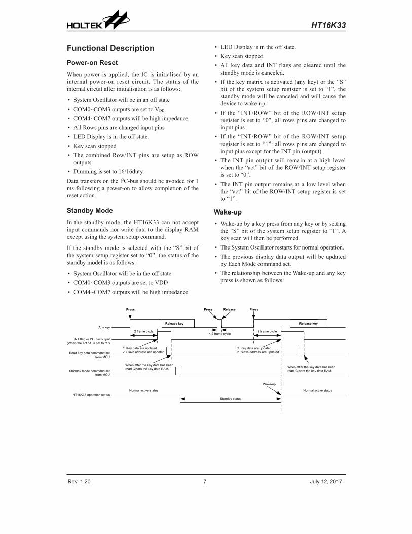
Wake-up• Wake-upbyakeypressfromanykeyorbysettingthe“S”bitof thesystemsetupregister to“1”.Akeyscanwillthenbeperformed.
• TheSystemOscillatorrestartsfornormaloperation.• ThepreviousdisplaydataoutputwillbeupdatedbyEachModecommandset.
• TherelationshipbetweentheWake-upandanykeypressisshownasfollows:
Wake-up
Standby mode command set from MCU
Read key data command set from MCU
INT flag or INT pin output
Any key
Press
Release key
2 frame cycle
Normal active statusHT16K33 operation status
Standby status
Press
2 frame cycle< 2 frame cycle
Release key
Normal active status
Press Release
(When the act bit is set to "1")1. Key data are updated2. Slave address are updated
1. Key data are updated2. Slave address are updated
When after the key data has been read,Clears the key data RAM. When after the key data has been
read, Clears the key data RAM.

Rev. 1.20 8 July 12, 2017
HT16K33
• Inthesleepmode,KS0-K1orKS1-K1cannotwake-upthedevicewhentheKS2-K1keysarekeptpresseddown.Itisaprohibitedapplicationasshowninthefollowingfigure.
COM1/KS0
COM2/KS1
COM3/KS2
Row0/K1 Row1/K2 Row2/K2
These key can not walk-up IC keep press down the key
System Setup RegisterThesystemsetupregisterconfiguressystemoperationorstandbyfortheHT16K33.
• Theinternalsystemoscillatorisenabledwhenthe‘S’bitofthesystemsetupregisterissetto“1”.• Theinternalsystemclockisdisabledandthedevicewillenterthestandbymodewhenthe“S”bitofthesystemsetupregisterissetto“0”.
• Beforethestandbymodecommandissent,itisstronglyrecommendedtoreadthekeydatafirst.• Thesystemsetupregistercommandisshownasfollows:
NameCommand / Address / Data
Option Description Def.D15 D14 D13 D12 D11 D10 D9 D8
System set 0 0 1 0 X X X S SWrite only
Definesinternalsystemoscillatoron/off.•0: Turn off System oscillator (standby
mode)•1:Turn on System oscillator (normal
operation mode)
20H
ROW/INT Set RegisterTheROW/INTsetupregistercanbesettoeitheranLEDRowoutput,oranINTlogicoutput.
• TheINToutputisselectedwhentheROW/INTsetregisterissetto“1”.• TheROWoutputisselectedwhentheROW/INTsetregisterissetto“0”.• The INT logicoutputcanbeconfiguredasan INToutput levelcontrolledby thekeyscancircuitryandcontrolledthroughthe2-wireinterface.
• TheINToutputisactive-lowwhenthe‘act’bitofROW/INTsetregisterissetto“0”.• TheINToutputisactive-highwhenthe‘act’bitofROW/INTsettregisterissetto“1”.• TheROW/INTsetupregistercommandisshownasfollows:

Rev. 1.20 9 July 12, 2017
HT16K33
NameCommand / Address / Data
Option Description Def.D15 D14 D13 D12 D11 D10 D9 D8
Row/int set 1 0 1 0 X X act row/int act, row/int Write only
DefinesINT/ROWoutputpinselectand INT pin output active level status.•X 0: INT/ROW output pin is set
to ROW driver output.•0, 1: INT/ROW output pin is set
to INT output, active low.•1, 1: INT/ROW output pin is set
to INT output, active high.
A0H
Display Setup RegisterThedisplaysetupregisterconfigurestheLEDdisplayon/offandtheblinkingfrequencyfortheHT16K33.
• TheLEDdisplayisenabledwhenthe‘D’bitofthedisplaysetupregisterissetto“1”.• TheLEDdisplayisdisabledwhenthe‘D’bitofthedisplaysetupregisterissetto“0”.• In thedisplaydisablestatus,allROWoutputsarehi-impedanceandallCOMoutputsarehigh-impedanceduringthedisplayperiod.
• In thedisplaydisablestatus,allROWsarechanged toan inputstatusand theCOM0~COM3continuesscanningandCOM4~COM7outputsarehigh-impedanceduringthekeyscanperiod.
• Thedisplayblinkingcapabilitiesof theHT16K33areveryversatile.Thewholedisplaycanbeblinkedatfrequenciesselectedby theBlinkcommand.Theblinkingfrequenciesare integermultiplesof thesystemfrequency;theratiosbetweenthesystemoscillatorandtheblinkingfrequenciesdependuponthemodeinwhichthedeviceisoperating,isasfollows:
• Blinkingfrequency=2Hz
Example of Waveform for Blinker
• Thedisplaysetupregistercommandisasfollows:
NameCommand / Address / Data
Option Description Def.D15 D14 D13 D12 D11 D10 D9 D8
Display set 1 0 0 0 X B1 B0 D
DWrite only
DefinesDisplayon/offstatus.•0: Display off •1: Display on
80HB1, B0
Write only
Definestheblinkingfrequency.•0,0 = Blinking OFF•0,1 = 2Hz•1,0 = 1Hz•1,1 = 0.5Hz

Rev. 1.20 10 July 12, 2017
HT16K33
System OscillatorTheinternal logicand theLEDdrivesignalsof theHT16K33aretimedbytheintegratedRCoscillator.
TheSystemClock frequencydetermines theLEDframe frequency.A clock signalmust always besuppliedtothedevice;removingtheclockmayfreezethedeviceifthestandbymodecommandisexecuted.Atinitialsystempoweron,theSystemOscillatorisinthestopstate.
Display Data Address PointerTheaddressingmechanismfor thedisplayRAMisimplementedusing theaddresspointer.Thisallowsthe loadingofan individualdisplaydatabyte,oraseriesofdisplaydatabytes, intoanylocationof thedisplayRAM.The sequencecommenceswith theinitialisationof theaddresspointerby theaddresspointercommand.
Key Data Address PointerTheaddressingmechanismforthekeydataRAMisimplementedusing theaddresspointer.Thisallowstheloadingofanindividualkeydatabyte,oraseriesofkeydatabytes, intoany locationof thekeydataRAM.Thesequencecommenceswith the initialisa-sa-a-tionof theaddresspointerby theAddresspointercommand.
Register Information Address PointerTheaddressingmechanismfor theregisterdataandInterruptflag informationRAMis implementedus-RAMis implementedus- implementedus-implementedus-us-ingtheaddresspointer.ThisallowstheloadingofanindividualregisterdataandInterruptflagdatabyte,oraseriesofregisterdataandInterruptflagdatabytes,intoanylocationoftheregisterdataandInterruptflaginformationRAM.ThesequencecommenceswiththeinitialisationoftheaddresspointerbytheAddresspointercommand.
Row Driver OutputsTheLEDdrive section includes16ROWoutputsROW0 toROW15which shouldbeconnecteddi-0 toROW15which shouldbeconnecteddi-ROW15which shouldbeconnecteddi-which shouldbeconnecteddi-di-di-rectlytotheLEDpanel.TheRowoutputsignalsare
generatedinaccordancewiththemultiplexedcolumnsignalsandwiththedataresidentinthedisplaylatch.Whenlessthan15ROWoutputsarerequiredtheun-15ROWoutputsarerequiredtheun-ROWoutputsarerequiredtheun-ROWoutputsarerequiredtheun-outputsarerequiredtheun-un-un-usedRowoutputsshouldbeleftopen-circuit.
Column Driver OutputsTheLEDdrivesectionincludeseightcolumnoutputsCOM0toCOM7whichshouldbeconnecteddirectlyto theLED panel.Thecolumnoutput signals aregeneratedinaccordancewiththeselectedLEDdrivemode.Whenlessthan8columnoutputsarerequiredtheunusedcolumnoutputsshouldbeleftopen-circuit.
Display Memory – RAM StructureThedisplayRAMisastatic16×8-bitRAMwhichstorestheLEDdata.Logic“1”intheRAMbit-mapindicates the“on”stateof thecorrespondingLEDRow;similarly,alogic0indicatesthe“off”state.
There isaone-to-onecorrespondencebetween theRAMaddressesand theRowoutputs,andbetweenthe individualbitsofaRAMwordand thecolumnoutputs.ThefollowingshowsthemappingfromtheRAMtotheLEDpattern:
COM0 ROW0 ROW7 ROW8 ROW15COM0 00H 01HCOM1 02H 03HCOM2 04H 05HCOM3 06H 07HCOM4 08H 09HCOM5 0AH 0BHCOM6 0CH 0DHCOM7 0EH 0FH
I2Cbusdisplaydatatransferformat.
Data byte of I2C D7 D6 D5 D4 D3 D2 D1 D0
ROW7 6 5 4 3 2 1 0
15 14 13 12 11 10 9 8

Rev. 1.20 11 July 12, 2017
HT16K33
LEDdrivemodewaveformsandscanningisasfollows:
• TheHT16K33allowsuseof1/9dutymodeandthecombinedROW/INTpinissettoaROWdriveroutputasshown:
ROW3/K1~ROW15/K13
1040μs
32μs1024μs
COM0(AD)
COM1(KS0)COM2(KS1)COM3(KS2)
COM4
COM5
COM6
COM7
16μs
16μs
1 Frame=1056μs*9=9.504ms
32μs
Hi-zHi-z
VDD
VSSVDD
VSSVDD
VSSVDD
VSSVDD
VSSVDD
VSSVDD
VSSVDD
VSSVDD
VSS
LOW
Hi-z
Hi-z
Hi-z
Hi-z
Hi-z
Hi-z
Hi-z
Hi-z
LOW
LOWHi
Hi
Hi
Hi-z
Hi-z
Hi-z
Hi-z
Hi-z
Hi-z
Hi-z
Hi-zLOW
LOW
LOW
LOW
LOW
LOW
LOW
Hi
LED Display periodKey scan
periodROW0/A2~ROW2/A0
Hi-z
• Keyscanperiodenlargement
COM1/KS0
COM2/KS1
C0M3/KS2
1024μs
VDD
VSSVDD
VSSVDD
VSS
Key scan period
Key data and Slave address are updated
Input status
VDD
VSS
256μs
ROW0/A2~ROW2/A0
256μs
256μs
VDD
VSSC0M4~COM6
Hi-Z
Hi-Z
Hi-Z
C0M7
32μs32μs
16μs
VSS
VDD
VDD
VSSCOM0/AD
Hi-Z
Hi-Z
Hi-Z
LowHigh
High
High
High256μs
Low
Hi-Z
Hi-Z
Hi-ZHi-ZROW3/K1~ROW15/K13
Hi-Z
Hi-Z
Note:TheROW/INcombinedpinissettoaRowdriveroutput.

Rev. 1.20 12 July 12, 2017
HT16K33
Digital Dimming Data InputTheDisplayDimmingcapabilitiesoftheHT16K33areveryversatile.ThewholedisplaycanbedimmedusingpulsewidthmodulationtechniquesfortheROWdriverbytheDimmingcommand,asshown:
D15 D14 D13 D12 D11 D10 D9 D8 ROW Driver Output Pulse Width Def.1 1 1 0 P3 P2 P1 P0 — —1 1 1 0 0 0 0 0 1/16 duty —1 1 1 0 0 0 0 1 2/16 duty —1 1 1 0 0 0 1 0 3/16 duty —1 1 1 0 0 0 1 1 4/16 duty —1 1 1 0 0 1 0 0 5/16 duty —1 1 1 0 0 1 0 1 6/16 duty —1 1 1 0 0 1 1 0 7/16 duty —1 1 1 0 0 1 1 1 8/16 duty —1 1 1 0 1 0 0 0 9/16 duty —1 1 1 0 1 0 0 1 10/16 duty —1 1 1 0 1 0 1 0 11/16 duty —1 1 1 0 1 0 1 1 12/16 duty —1 1 1 0 1 1 0 0 13/16 duty —1 1 1 0 1 1 0 1 14/16 duty —1 1 1 0 1 1 1 0 15/16 duty —1 1 1 0 1 1 1 1 16/16 duty Y

Rev. 1.20 13 July 12, 2017
HT16K33
TherelationshipbetweenROWandCOMDigitalDimmingdutytimeisasfollows:
ROW(n)
1024μs
1/16 duty
3/16 duty
4/16 duty
5/16 duty
6/16 duty
7/16 duty
8/16 duty
9/16 duty
10/16 duty
11/16 duty
12/16 duty
13/16 duty
14/16 duty
15/16 duty
16/16 duty
2/16 duty
1040μsCOM(n)
Rev. 1.20 14 July 12, 2017
HT16K33
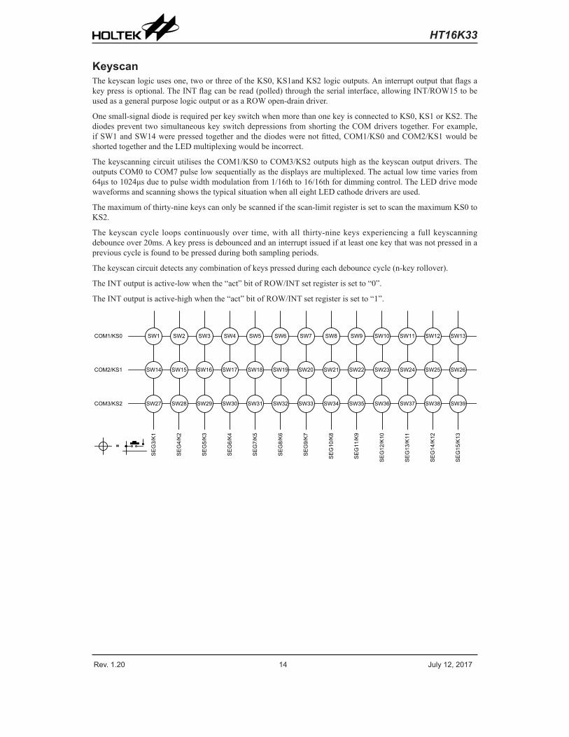
KeyscanThekeyscanlogicusesone,twoorthreeoftheKS0,KS1andKS2logicoutputs.Aninterruptoutputthatflagsakeypressisoptional.TheINTflagcanberead(polled)throughtheserialinterface,allowingINT/ROW15tobeusedasageneralpurposelogicoutputorasaROWopen-draindriver.
Onesmall-signaldiodeisrequiredperkeyswitchwhenmorethanonekeyisconnectedtoKS0,KS1orKS2.ThediodespreventtwosimultaneouskeyswitchdepressionsfromshortingtheCOMdriverstogether.Forexample,ifSW1andSW14werepressedtogetherandthediodeswerenotfitted,COM1/KS0andCOM2/KS1wouldbeshortedtogetherandtheLEDmultiplexingwouldbeincorrect.
ThekeyscanningcircuitutilisestheCOM1/KS0toCOM3/KS2outputshighasthekeyscanoutputdrivers.TheoutputsCOM0toCOM7pulselowsequentiallyasthedisplaysaremultiplexed.Theactuallowtimevariesfrom64μsto1024μsduetopulsewidthmodulationfrom1/16thto16/16thfordimmingcontrol.TheLEDdrivemodewaveformsandscanningshowsthetypicalsituationwhenalleightLEDcathodedriversareused.
Themaximumofthirty-ninekeyscanonlybescannedifthescan-limitregisterissettoscanthemaximumKS0toKS2.
Thekeyscancycle loopscontinuouslyover time,withall thirty-ninekeysexperiencinga fullkeyscanningdebounceover20ms.Akeypressisdebouncedandaninterruptissuedifatleastonekeythatwasnotpressedinapreviouscycleisfoundtobepressedduringbothsamplingperiods.
Thekeyscancircuitdetectsanycombinationofkeyspressedduringeachdebouncecycle(n-keyrollover).
TheINToutputisactive-lowwhenthe“act”bitofROW/INTsetregisterissetto“0”.
TheINToutputisactive-highwhenthe“act”bitofROW/INTsetregisterissetto“1”.
COM1/KS0
COM2/KS1
COM3/KS2
SE
G3/
K1
SE
G4/
K2
SE
G5/
K3
SE
G6/
K4
SE
G7/
K5
SE
G8/
K6
SE
G9/
K7
SE
G10
/K8
SE
G11
/K9
SE
G12
/K10
SE
G14
/K12
SE
G15
/K13
SE
G13
/K11
=
SW1
SW14
SW27
SW2 SW3 SW4 SW5 SW6 SW7 SW8 SW9 SW10 SW11 SW12 SW13
SW15 SW16 SW17 SW18 SW19 SW20 SW21 SW22 SW23 SW24 SW25 SW26
SW28 SW29 SW30 SW31 SW32 SW33 SW34 SW35 SW36 SW37 SW38 SW39
Rev. 1.20 15 July 12, 2017
HT16K33
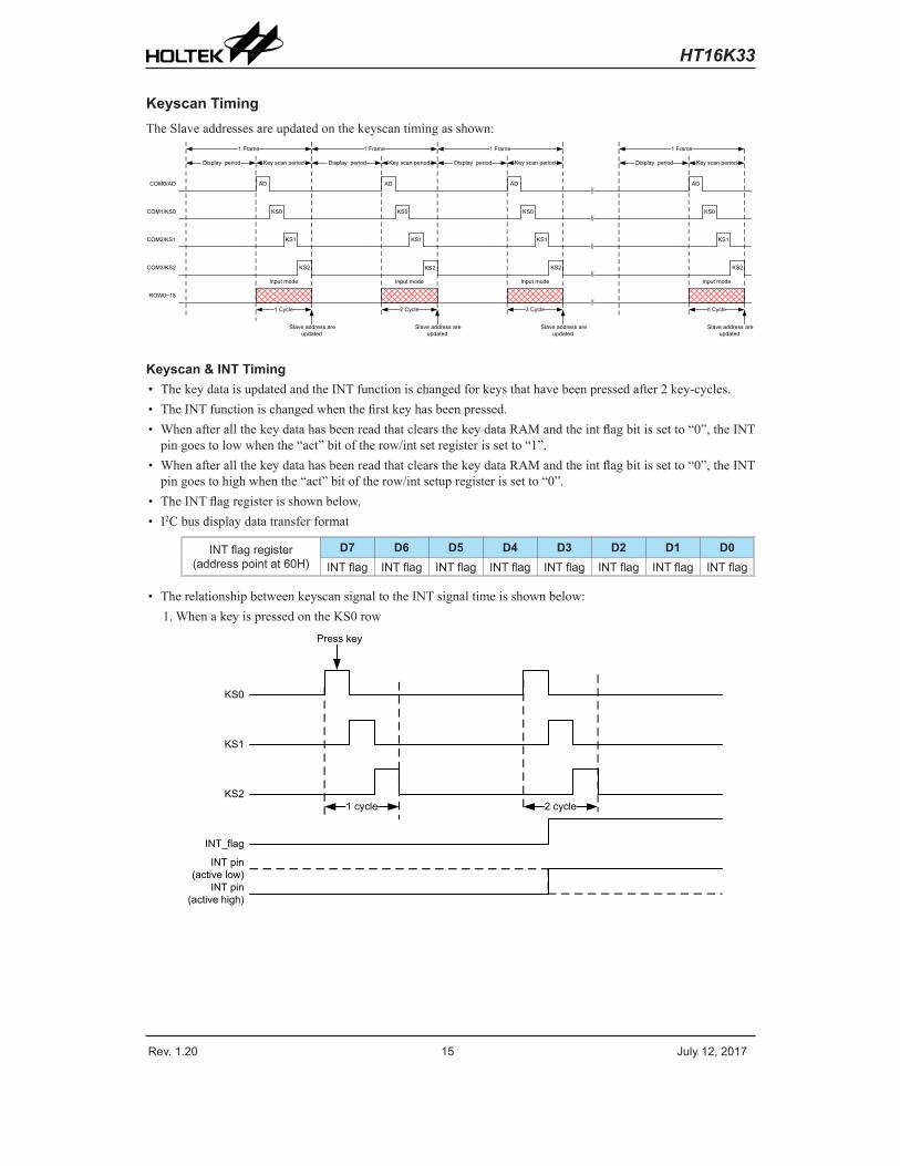
Keyscan TimingTheSlaveaddressesareupdatedonthekeyscantimingasshown:
KS0
KS1
KS2
Input mode
COM1/KS0
COM2/KS1
COM3/KS2
ROW0~15
1 Cycle
Key scan periodDisplay period
1 Frame
∫∫
Slave address are updated
Slave address are updated
Slave address are updated
AD
KS0
KS1
Input mode
2 Cycle
Key scan periodDisplay period
1 Frame
AD
KS0
KS1
KS2
Input mode
3 Cycle
Key scan periodDisplay period
1 Frame
Slave address are updated
AD
∫∫
∫∫
∫∫
∫∫
KS0
KS1
KS2
Input mode
n Cycle
Key scan periodDisplay period
1 Frame
ADCOM0/AD
KS2
Keyscan & INT Timing• ThekeydataisupdatedandtheINTfunctionischangedforkeysthathavebeenpressedafter2key-cycles.• TheINTfunctionischangedwhenthefirstkeyhasbeenpressed.• WhenafterallthekeydatahasbeenreadthatclearsthekeydataRAMandtheintflagbitissetto“0”,theINTpingoestolowwhenthe“act”bitoftherow/intsetregisterissetto“1”.
• WhenafterallthekeydatahasbeenreadthatclearsthekeydataRAMandtheintflagbitissetto“0”,theINTpingoestohighwhenthe“act”bitoftherow/intsetupregisterissetto“0”.
• TheINTflagregisterisshownbelow.• I2Cbusdisplaydatatransferformat
INTflagregister(address point at 60H)
D7 D6 D5 D4 D3 D2 D1 D0INTflag INTflag INTflag INTflag INTflag INTflag INTflag INTflag
• TherelationshipbetweenkeyscansignaltotheINTsignaltimeisshownbelow:1.WhenakeyispressedontheKS0row
KS0
KS1
KS2
Press key
INT_flag
1 cycle 2 cycle
INT pin(active low)
INT pin(active high)

Rev. 1.20 16 July 12, 2017
HT16K33
2.WhenakeyispressedontheKS1row
KS0
KS1
KS2
Press key
INT_flag
1 cycle 2 cycle
INT pin(active low)
INT pin(active high)
3.WhenakeyispressedontheKS2row
KS0
KS1
KS2
Press key
INT_flag
1 cycle 2 cycle
INT pin(active low)
INT pin(active high)
• Keypressedduringakeyscancycleperiod.(i.e.thekeyispressedontheKS2row)
The key data are updated when the interrupt asserted if required.
1 Cycle 2 Cycle 3 Cycle 4 Cycle
Press first key
Keyscan
INT flag
INT pin(active low)
INT pin(active high)
Release key
When after the all key data has been read: 1. Clears the key data RAM.2. The INT flag bit is set to "0".3. The INT pin goes to low when "act" bit is set to "1".4. The INT pin goes to high when "act" bit is ise to "0".
5 Cycle 6 Cycle
Press second key Key data are updatedRelease key
7 Cycle
Key scan period
Rev. 1.20 17 July 12, 2017
HT16K33
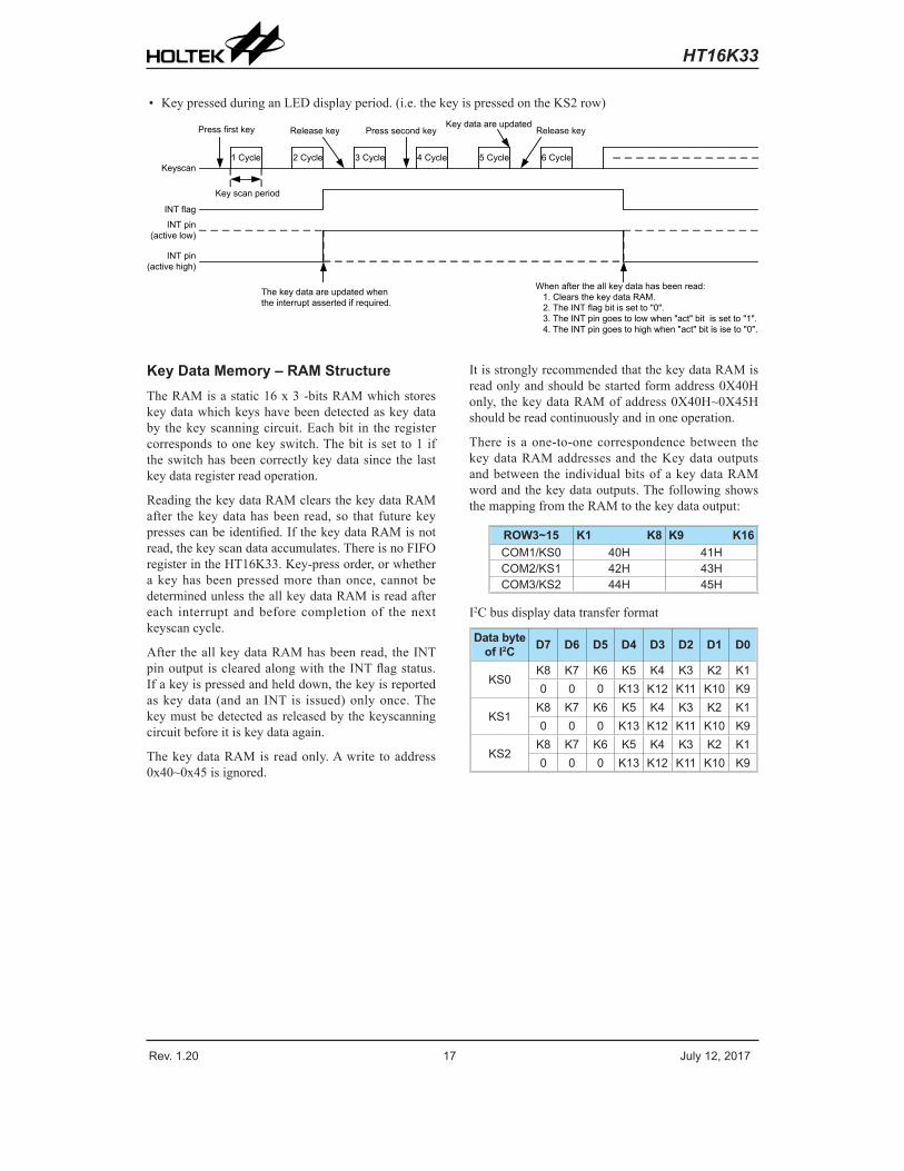
• KeypressedduringanLEDdisplayperiod.(i.e.thekeyispressedontheKS2row)
1 Cycle 2 Cycle 3 Cycle 4 Cycle
Press first key
Keyscan
INT flag
INT pin(active low)
INT pin(active high)
Release key
When after the all key data has been read: 1. Clears the key data RAM.2. The INT flag bit is set to "0".3. The INT pin goes to low when "act" bit is set to "1".4. The INT pin goes to high when "act" bit is ise to "0".
5 Cycle 6 Cycle
The key data are updated when the interrupt asserted if required.
Key data are updatedRelease key Press second key
Key scan period
Key Data Memory – RAM StructureTheRAMisastatic16x3-bitsRAMwhichstoreskeydatawhichkeyshavebeendetectedaskeydataby thekeyscanningcircuit.Eachbit in theregistercorresponds toonekeyswitch.Thebit isset to1iftheswitchhasbeencorrectlykeydatasincethelastkeydataregisterreadoperation.
ReadingthekeydataRAMclearsthekeydataRAMafter thekeydatahasbeenread,so that futurekeypressescanbeidentified.IfthekeydataRAMisnotread,thekeyscandataaccumulates.ThereisnoFIFOregisterintheHT16K33.Key-pressorder,orwhetherakeyhasbeenpressedmore thanonce,cannotbedeterminedunlesstheallkeydataRAMisreadaftereach interrupt andbefore completionof thenextkeyscancycle.
After theallkeydataRAMhasbeenread, theINTpinoutput isclearedalongwiththeINTflagstatus.Ifakeyispressedandhelddown,thekeyisreportedaskeydata (andan INT is issued)onlyonce.Thekeymustbedetectedasreleasedbythekeyscanningcircuitbeforeitiskeydataagain.
ThekeydataRAMisreadonly.Awrite toaddress0x40~0x45isignored.
ItisstronglyrecommendedthatthekeydataRAMisreadonlyandshouldbestartedformaddress0X40Honly, thekeydataRAMofaddress0X40H~0X45Hshouldbereadcontinuouslyandinoneoperation.
There isaone-to-onecorrespondencebetween thekeydataRAMaddressesand theKeydataoutputsandbetweenthe individualbitsofakeydataRAMwordandthekeydataoutputs.ThefollowingshowsthemappingfromtheRAMtothekeydataoutput:
ROW3~15 K1 K8 K9 K16COM1/KS0 40H 41HCOM2/KS1 42H 43HCOM3/KS2 44H 45H
I2Cbusdisplaydatatransferformat
Data byte of I2C D7 D6 D5 D4 D3 D2 D1 D0
KS0K8 K7 K6 K5 K4 K3 K2 K10 0 0 K13 K12 K11 K10 K9
KS1K8 K7 K6 K5 K4 K3 K2 K10 0 0 K13 K12 K11 K10 K9
KS2K8 K7 K6 K5 K4 K3 K2 K10 0 0 K13 K12 K11 K10 K9

Rev. 1.20 18 July 12, 2017
HT16K33
Key Matrix ConfigurationAnexampleofkeymatrixconfigurationsisshownbelow.
When pressing three or more times is assumedAconfigurationexampleisshownbelow.Inthisconfiguration,1to39ONswitchescanberecognised.
KS0
KS1
KS2
K1 K2 K3 K4 K5 K6 K7 K8 K9 K10 K11 K12 K13
=
When pressing twice or more times is assumedAconfigurationexampleisshownbelow.Inthisconfiguration,0to2ONswitchescanberecognised.
KS0
KS1
KS2
K1 K2 K3 K4 K5 K6 K7 K8 K9 K10 K11 K12 K13
=
Inthisconfiguration,pressingthreeormoretimesmaycausetheOFFswitchestobedeterminedasbeingON.
Forexample,ifSW2,SW4areONandKS0hasbeenselected(highlevel)asshownbelow,SW3,inwhichcurrentI1isrunningissupposedtobedetectedtobeON.However,sinceSW2andSW4areON,currentI2runsthusresultinginSW1toberecognisedasbeingON(ghostkey).
KS0
KS1
KS2
K1 K2 K3 K4 K5 K6 K7 K8 K9 K10 K11 K12 K13
=
SW1 SW3
SW2 SW4
Select
I1I2

Rev. 1.20 19 July 12, 2017
HT16K33
Ifadiodeisnotavailable,notonlythekeydatamaynotbereadnormallybuttheLEDdisplaymaybeaffectedortheICsmaybedamaged.
Forexample,ifSW1andSW2areONandKS0hasbeenselected(highlevel)asshownbelow,thiswillcausenotonlycurrentI1whichissupposedtorunbutalsoashort-circuitcurrentI2ofKS0toKS1toflow.
Itispossiblethatthiswillthencausethefollowingtwoproblems:
(1)SincetheleveltoK2isnotcorrectlysent,thekeydatacannotbelatchedcorrectly.
(2)Sincetheshort-circuitedcurrent(currentI2)ofKS1(highlevel)toKS1(lowlevel)flows,thedevicemaybedamaged.
KS0
KS1
KS2
K1 K2 K3 K4 K5 K6 K7 K8 K9 K10 K11 K12 K13
=
SW1
SW2
Select
I1
I2Nonselect
Key Matrix Combination with 28-pin Package
Without INT pin
COM1/KS0
COM2/KS1
COM3/KS2
SEG
3/K1
SEG
4/K2
SEG
5/K3
SEG
6/K4
SEG
7/K5
SEG
8/K6
SEG
9/K7
SEG
10/K8
SEG
11/K9
SEG
12/K10
SEG
14/K12
SEG
15/K13
SEG
13/K11
=
With INT pin
COM1/KS0
COM2/KS1
COM3/KS2
SEG
3/K1
SEG
4/K2
SEG
5/K3
SEG
6/K4
SEG
7/K5
SEG
8/K6
SEG
9/K7
SEG
10/K8
SEG
11/K9
SEG
12/K10
SEG
14/K12
SEG
13/K11
=

Rev. 1.20 20 July 12, 2017
HT16K33
Key matrix combination with 24-pin package
Without INT pin
COM1/KS0
COM2/KS1
COM3/KS2
SEG
3/K1
SEG
4/K2
SEG
5/K3
SEG
6/K4
SEG
7/K5
SEG
8/K6
SEG
9/K7
SEG
10/K8
SEG
11/K9
SEG
12/K10
=
With INT pin
COM1/KS0
COM2/KS1
COM3/KS2
SEG
3/K1
SEG
4/K2
SEG
5/K3
SEG
6/K4
SEG
7/K5
SEG
8/K6
SEG
9/K7
SEG
10/K8
SEG
11/K9
=
Key matrix combination with 20-pin package
Without INT pin
COM1/KS0
COM2/KS1
COM3/KS2
SEG
3/K1
SEG
4/K2
SEG
5/K3
SEG
6/K4
SEG
7/K5
SEG
8/K6
SEG
9/K7
SEG
10/K8
=

Rev. 1.20 21 July 12, 2017
HT16K33
With INT pin
COM1/KS0
COM2/KS1
COM3/KS2
SEG
3/K1
SEG
4/K2
SEG
5/K3
SEG
6/K4
SEG
7/K5
SEG
8/K6
SEG
9/K7
=
I2C Serial InterfaceTheHT16K33includesanI2Cserial interface.TheI2Cbus isusedforbidirectional, two-linecommu-commu-nicationbetweendifferentICsormodules.Thetwolinesareaserialdataline(SDA)andaserialclockline (SCL).Both linesareconnected toapositivesupplyviaapull-upresistor.Whenthebus is free,both lines arehigh.Theoutput stagesofdevicesconnected to thebusmusthaveanopen-drainoropen-collectortoperformawiredandfunction.Datatransferisinitiatedonlywhenthebusisnotbusy.
Data ValidityThedataontheSDAlinemustbestableduringthehighperiodoftheclock.Thehighorlowstateofthedata linecanonlychangewhentheclocksignalontheSCLlineisLow(seebelow).
SDA
SCL
Data line stable,Data valid
Chang of data allowed
START and STOP Conditions• Ahigh to low transitionon theSDAlinewhileSCLishighdefinesaSTARTcondition.
• A low tohigh transitionon theSDAlinewhileSCLishighdefinesaSTOPcondition.
• STARTandSTOPconditionsarealwaysgeneratedby themaster.Thebus isconsidered tobebusyaftertheSTARTcondition.Thebusisconsideredtobe free againa certain timeafter theSTOPcondition.
• Thebusstaysbusy ifa repeatedSTART(Sr) isgenerated insteadofaSTOPcondition. In thisrespect, theSTART(S)andrepeatedSTART(Sr)conditionsarefunctionallyidentical.
PS
SDA
SCL
SDA
SCL
START condition STOP condition
Byte FormatEverybyteputontheSDAlinemustbe8-bitslong.Thenumberof bytes that canbe transmittedpertransferisunrestricted.Eachbytehastobefollowedbyanacknowledgebit.Data is transferredwith themostsignificantbit(MSB)first.
SorSr
PorSr
SDA
SCL 1 2 7 8 9
ACK
1 2 3-8 9
ACK
P
Sr
Acknowledge• Eachbytes includeseightbits is followedbyasingleacknowledgebit.Thisacknowledgebit isalowlevelputonthebusbythereceiver,themastergenerates an extra acknowledge related clockpulse.
• Aslavereceiverwhichisaddressedmustgenerateanacknowledge(ACK)afterthereceptionofeachbyte.
• ThedevicethatacknowledgemustpulldowntheSDAlineduringtheacknowledgeclockpulsesothatitremainsstablelowduringthehighperiodofthisclockpulse.
• Amasterreceivermustsignalanendofdatatotheslavebygeneratinganot-acknowledge(NACK)biton the lastbyte thathasbeenclockedoutoftheslave. In thiscase, themaster receivermustleavethedatalinehighduringthe9thpulsetonotacknowledge.ThemasterwillgenerateaSTOPorrepeatedSTARTcondition.
Rev. 1.20 22 July 12, 2017
HT16K33
S1 2 7 8 9
CLK pulse foracknowledgement
Data OutputBy Transmiter
Data OutputBy Receiver
SCL FromMaster
acknowledge
not acknowledge
STARTcondition
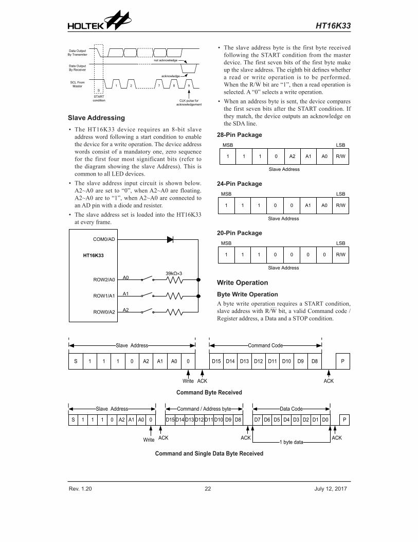
Slave Addressing• TheHT16K33 device requires an 8-bit slaveaddresswordfollowingastartconditiontoenablethedeviceforawriteoperation.Thedeviceaddresswordsconsistofamandatoryone,zerosequencefor the first fourmost significantbits (refer tothediagramshowing theslaveAddress).This iscommontoallLEDdevices.
• Theslaveaddress inputcircuit is shownbelow.A2~A0areset to“0”,whenA2~A0arefloating.A2~A0are to“1”,whenA2~A0areconnectedtoanADpinwithadiodeandresister.
• Theslaveaddresssetisloaded intotheHT16K33ateveryframe.
ROW2/A0
ROW1/A1
ROW0/A2
A0
A1
A2
HT16K33
COM0/AD
39kΩ×3
• Theslaveaddressbyte is the firstbyte receivedfollowing theSTARTcondition fromthemasterdevice.Thefirstsevenbitsof thefirstbytemakeuptheslaveaddress.Theeighthbitdefineswhethera read orwrite operation is to be performed.WhentheR/Wbitare“1”,thenareadoperationisselected.A“0”selectsawriteoperation.
• Whenanaddressbyteissent,thedevicecomparesthefirstsevenbitsafter theSTARTcondition. Iftheymatch,thedeviceoutputsanacknowledgeontheSDAline.
28-Pin Package
1 1 1 0 A2 A1 A0 R/W
MSB LSB
Slave Address
24-Pin Package
1 1 1 0 0 A1 A0 R/W
MSB LSB
Slave Address
20-Pin Package
1 1 1 0 0 0 0 R/W
MSB LSB
Slave Address
Write OperationByte Write OperationAbytewriteoperationrequiresaSTARTcondition,slaveaddresswithR/Wbit,avalidCommandcode/Registeraddress,aDataandaSTOPcondition.
Slave Address
ACKWrite
Command Code
ACK
PS 1 1 1 0 A2 A1 A0 0 D15 D14 D13 D12 D11 D10 D9 D8
Command Byte Received
Slave Address
ACKWrite
Command / Address byte
ACK
S 1 1 1 0 A2 A1 A0 0 D15 D14 D13 D12 D11 D10 D9 D8
Data Code
ACK
PD7 D6 D5 D4 D3 D2 D1 D0
1 byte data
Command and Single Data Byte Received

Rev. 1.20 23 July 12, 2017
HT16K33
Page Write OperationFollowingaSTARTconditionandslaveaddresswithR/WbitisplacedonthebusandindicatestotheaddresseddevicethatRegisterAddresswillfollowandistobewrittentotheaddresspointer.Thedatatobewrittentothememoryinnextandtheinternaladdresspointerisincrementedtothenextaddresslocationonthereceptionofanacknowledgeclock.Afterreachingthedisplaymemorylocation0X0FHthepointerwillresetto0X00H(displaymemory).
Slave Address
ACKWrite
Command/register Address byte
ACK
S 1 1 1 0 A2 A1 A0 0 D15 D14 D13 D12 D11 D10 D9 D8
Data byte
ACK
PD7 D6 D5 D4 D3 D2 D1 D0
n bytes data
Data byte
D7 D6 D5 D4 D3 D2 D1 D0
First byte dataACK
Data byte
D7 D6 D5 D4 D3 D2 D1 D0
Second byte data∫∫
ACK
N Data Bytes Received
Read Operation
Byte Read Operation• AbytereadoperationrequiresaSTARTcondition,slaveaddresswithR/Wbit,afixvalidRegisteraddress,slaveaddresswithRbit,aDataandaNACKsignalandaSTOPcondition.
• TheBytereadscommandisnotavailableforKeydatareading.Slave Address
ACKWrite
Command/register address byte
ACK
S 1 1 1 0 A2 A1 A0 0 D15 D14 D13 D12 D11 D10 D9 D8
Slave Address
Read
S 1 1 1 0 A2 A1 A0 1P
ACK
Data byte
D7 D6 D5 D4 D3 D2 D1 D0
1 byte data
P
NACK
Reading Single Data Bytes from the HT16K33
Page Read Operation• Inthismode,themasterreadstheHT16K33dataaftersettingtheslaveaddress.FollowingaR/Wbit(=“0”)andacknowledgebit,theregisteraddress(An)iswrittentotheaddressWpointer.NexttheSTARTconditionandslaveaddressarerepeatedfollowedbyaR/Wbit(=“1”).Thedatawhichwasaddressedisthentransmitted.Theaddresspointerisonlyincrementedonreceptionofanacknowledgeclock.TheHT16K33willplacethedataataddressAn+1onthebus.Themasterreadsandacknowledgesthenewbyteandtheaddresspointerisincrementedto“An+2”.
• Iftheregisteraddress(An)is0X00h~0X0Fh,afterreachingthememorylocation0X0Fh,thepointerwillberesetto0X00h.
• ThekeydataRAMofaddress0x40H~0x45Hshouldbereadcontinuouslyandcompletedinoneoperation,sothekeydataRAMofaddressshouldbestartedfrom0x40Honly.
• Thiscycleofreadingconsecutiveaddresseswillcontinueuntil themastersendsaNACKsignalandSTOPcondition.
Slave Address
ACKWrite
Command/register address byte
ACK
S 1 1 1 0 A2 A1 A0 0 D15 D14 D13 D12 D11 D10 D9 D8
Data byte
NACK
PD7 D6 D5 D4 D3 D2 D1 D0
n bytes data
Slave Address
Read
S 1 1 1 0 A2 A1 A0 1P
ACK
Data byte
D7 D6 D5 D4 D3 D2 D1 D0
First byte data ACK
Data byte
D7 D6 D5 D4 D3 D2 D1 D0
Second byte data∫∫
ACK
Reading n Data Bytes from the HT16K33

Rev. 1.20 24 July 12, 2017
HT16K33
Command Summary
NameCommand / Address
Option Description Def.D15 D14 D13 D12 D11 D10 D9 D8
Display data
Address pointer
0 0 0 0 A3 A2 A1 A0 A0~A3R/W
•Five bits of immediate data, bits A0 to A3, are transferred to the data pointer to define one of sixteen display RAM addresses.
•If the Display data register address (An) is 0X00h~0X0Fh, after reaching the memory location 0X0Fh, the pointer will reset to 0X00h
00H
System setup 0 0 1 0 X X X S S
Write only
Definesinternalsystemoscillatoron/off•0:Turn off System oscillator (standby
mode)•1:Turn on System oscillator (normal
operation mode)
20H
Key data Address pointer
0 1 0 0 0 K2 K1 K0 K0~K2Read only
•Three bits of immediate data, bits K0 to K2, are transferred to the data pointer to define one of six key data RAM addresses.
•It is strongly recommended that the key data RAM of address 0x40h~0x45h should be read continuously and in one operation, so the key data RAM of address should be started at 0x40H only.
•If the Key data register address (An) is 0X40h~0X45h, after reaching the memory location 0X45h, the pointer will reset to 0X40h
40H
INTflagAddress pointer
0 1 1 0 0 0 0 0 Read only
Defines the INT flag address, Read INT flagstatus.Interruptflagsignaloutput.Whenanykeymatrix key is pressed, after the completion of two key scan cycles, this int flag bit goes to a high level and remains at a high level until all key data has been read,
60H
Display setup 1 0 0 0 X B1 B0 D
DWrite only
DefinesDisplayon/offstatus.•0: Display off •1: Display on
80HB1, B0
Write only
Definestheblinkingfrequency•0,0 = Blinking OFF•0,1 = 2Hz•1,0 = 1Hz•1,1 = 0.5Hz
ROW/INT set 1 0 1 0 X X act row/
int
act, row/int
Write only
DefinesINT/ROWoutputpinselectandINT pin output active level status.•X 0: INT/ROW output pin is set to
ROW driver output.•0,1: INT/ROW output pin is set to INT
output, active low.•1,1: INT/ROW output pin is set to INT
output, active high.
A0H

Rev. 1.20 25 July 12, 2017
HT16K33
NameCommand / Address
Option Description Def.D15 D14 D13 D12 D11 D10 D9 D8
Dimming set 1 1 1 0 P3 P2 P1 P0 P3~P0
Write only
DefinesthepulsewidthofROW.•0,0,0,0: 1/16duty•0,0,0,1: 2/16duty•0,0,1,0: 3/16duty•0,0,1,1: 4/16duty•0,1,0,0: 5/16duty•0,1,0,1: 6/16duty•0,1,1,0: 7/16duty•0,1,1,1: 8/16duty•1,0,0,0: 9/16duty•1,0,0,1: 10/16duty•1,0,1,0: 11/16duty•1,0,1,1: 12/16duty•1,1,0,0: 13/16duty•1,1,0,1: 14/16duty•1,1,1,0: 15/16duty•1,1,1,1: 16/16duty
EFH
Test mode 1 1 0 1 1 0 0 1 Write only HOLTEK use only D9H
Note:Ifaprogrammedcommanddataisnotdefined,thefunctionwillnotbeaffected.
Operation Flow ChartAccessproceduresareillustratedbelowbymeansofflowcharts.
Initialisation
Power On
END
ROW/INT output pin setINT pin output level set
Dimming set
Internal system clock enable
Blinking set

Rev. 1.20 26 July 12, 2017
HT16K33
Display data rewrite – address setting
Start
Next processing
Display data RAM write
Address setting
Display on
Key data read
no
yes
Start
Int flag bit =1 ?
Read Key data
Next processing
row/int select Register setINT / ROW bit=1?
yes no
Clear int flagand the key data RAM
no
yes
Int pin bit =1 ?
Read Key data
Next processing
INT pin is set to low level and clears the key data RAM
no
yes
Int pin bit =0 ?
Read Key data
Next processing
INT pin is set to high leveland clears the key data RAM
“act” bit is set to “0”=?
yes
no
Read Key data
Next processing
Clear int flagand clears the key data RAM
no

Rev. 1.20 27 July 12, 2017
HT16K33
Application Circuits16×8 display application: (No INT pin function and 13×3 key function)
LED matrix
SCL
SDA
VDD
VSS
MCU
VDD
VSS
HT16K33
VSS
0.1μF
COM0COM1/KS0COM2/KS1COM3/KS2
COM4COM5COM6COM7
VDD
Row13/K11Row14/K12
Row12/K10Row11/K9Row10/K8
Row9/K7Row8/K6Row7/K5Row6/K4Row5/K3Row4/K2Row3/K1Row2/A0Row1/A1Row0/A2
Row15/K13/INT39kΩ×13
=
R1R2R3R4R5R6R7R8R9R10R11R12R13
4.7kΩ4.7kΩ
RA0 RA1 RA2
Note:1.IfRA0,RA1andRA2areOpen,theI2Cslaveaddress(A0~A2)issettolow.2.IfRA0,RA1andRA2are39kΩ,theI2Cslaveaddress(A0~A2)issettohigh.
3.If thekeyinputisnotusedforLEDdisplay, theresistor inserieswiththekeyinput(R1~R13)canbeomitted.
15×8 display application: (INT pin function and 12×3 key function)
LED matrix
SCL
SDA
VDD
VSS
MCU
VDD
VSS
HT16K33
VSS
0.1μF
=
COM0COM1/KS0COM2/KS1COM3/KS2
COM4COM5COM6COM7
VDD
Row13/K11Row14/K12
Row15/K13/INT
Row12/K10Row11/K9Row10/K8
Row9/K7Row8/K6Row7/K5Row6/K4Row5/K3Row4/K2Row3/K1Row2/A0Row1/A1Row0/A2
39kΩ×12
4.7kΩ4.7kΩ
R1R2R3R4R5R6R7R8R9R10R11R12
RA0 RA1 RA2
Note:1.IfRA0,RA1andRA2areOpen,theI2Cslaveaddress(A0~A2)issettolow.2.IfRA0,RA1andRA2are39kΩ,theI2Cslaveaddress(A0~A2)issettohigh.3.If thekeyinputisnotusedforLEDdisplay, theresistor inserieswiththekeyinput(R1~R12)canbeomitted.
Rev. 1.20 28 July 12, 2017
HT16K33
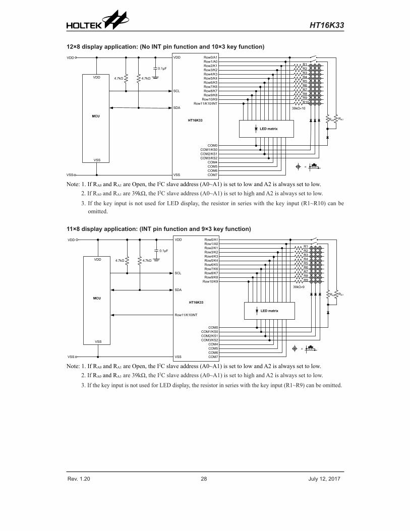
12×8 display application: (No INT pin function and 10×3 key function)
LED matrix
SCL
SDA
VDD
VSS
MCU
VDD
VSS
HT16K33
VSS
0.1μF
COM0COM1/KS0COM2/KS1COM3/KS2
COM4COM5COM6COM7
VDD
Row11/K10/INTRow10/K9
Row9/K8Row8/K7Row7/K6Row6/K5Row5/K4Row4/K3Row3/K2Row2/K1Row1/A0Row0/A1
39kΩ×10
=
R1R2R3R4R5R6R7R8R9R10
4.7kΩ4.7kΩ
RA0 RA1
Note:1.IfRA0andRA1areOpen,theI2Cslaveaddress(A0~A1)issettolowandA2isalwayssettolow.2.IfRA0andRA1are39kΩ,theI2Cslaveaddress(A0~A1)issettohighandA2isalwayssettolow.
3.If thekeyinputisnotusedforLEDdisplay, theresistorinserieswiththekeyinput(R1~R10)canbeomitted.
11×8 display application: (INT pin function and 9×3 key function)
LED matrix
SCL
SDA
VDD
VSS
HT16K33
COM0COM1/KS0COM2/KS1COM3/KS2
COM4COM5COM6COM7
Row11/K10INT
Row10/K9Row9/K8Row8/K7Row7/K6Row6/K5Row5/K4Row4/K3Row3/K2Row2/K1Row1/A0Row0/A1
MCU
VDD
VSS
VSS
4.7kΩ
0.1μF
VDD
39kΩ×9
=
4.7kΩ
R1R2R3R4R5R6R7R8R9
RA0 RA1
Note:1.IfRA0andRA1areOpen,theI2Cslaveaddress(A0~A1)issettolowandA2isalwayssettolow.2.IfRA0andRA1are39kΩ,theI2Cslaveaddress(A0~A1)issettohighandA2isalwayssettolow.
3.IfthekeyinputisnotusedforLEDdisplay,theresistorinserieswiththekeyinput(R1~R9)canbeomitted.

Rev. 1.20 29 July 12, 2017
HT16K33
8×8 display application: (No INT pin function and 8×3 key function)
LED matrix
SCL
SDA
VDD
VSS
MCU
VDD
VSS
HT16K33
VSS
0.1μF
COM0COM1/KS0COM2/KS1COM3/KS2
COM4COM5COM6COM7
VDD
Row7/K8/INTRow6/K7Row5/K6Row4/K5Row3/K4Row2/K3Row1/K2Row0/K1
39kΩ×8
=
R1R2R3R4R5R6R7R8
4.7kΩ4.7kΩ
Note:1.TheI2Cslaveaddress(A0~A2)=000.2.IfthekeyinputisnotusedforLEDdisplay,theresistorinserieswiththekeyinput(R1~R8)canbeomit-
ted.
7×8 display application: (INT pin function and 7×3 key function)
LED matrix
SCL
SDA
VDD
VSS
MCU
VDD
VSS
HT16K33
0.1μF
COM0COM1/KS0COM2/KS1COM3/KS2
COM4COM5COM6COM7
Row7/K8/INT
Row6/K7Row5/K6Row4/K5Row3/K4Row2/K3Row1/K2Row0/K1
39kΩ×7
=VSS
VDDR1R2R3R4R5R6R7
4.7kΩ4.7kΩ
Note:1.TheI2Cslaveaddress(A0~A2)=000.2.IfthekeyinputisnotusedforLEDdisplay,theresistorinserieswiththekeyinput(R1~R7)canbeomitted.

Rev. 1.20 30 July 12, 2017
HT16K33
LED Matrix Circuit
COM0 COM1 COM6 COM7
ROW0
ROW1
ROW2
ROW3
ROW4
ROW5
ROW6
ROW7
ROW8
ROW9
ROW10
ROW11
ROW12
ROW13
ROW14
ROW15
DisplayRAMdatashouldbeinitialized(clearallRAMdata)beforetheyareused.UseofanuninitializedRAMdatawillcausethedisplayimpropervalues.

Rev. 1.20 31 July 12, 2017
HT16K33
Package Information
Notethat thepackageinformationprovidedhereisforconsultationpurposesonly.Asthis informationmaybeupdatedatregularintervalsusersareremindedtoconsulttheHoltekwebsiteforthelatestversionofthePackage/CartonInformation.
Additionalsupplementaryinformationwithregardtopackagingislistedbelow.Clickontherelevantsectiontobetransferredtotherelevantwebsitepage.
• PackageInformation(includeOutlineDimensions,ProductTapeandReelSpecifications)
• TheOperationInstructionofPackingMaterials
• Cartoninformation

Rev. 1.20 32 July 12, 2017
HT16K33
20-pin SOP (300mil) Outline Dimensions
SymbolDimensions in inch
Min. Nom. Max.A — 0.406 BSC —B — 0.295 BSC —C 0.012 — 0.020 C’ — 0.504 BSC —D — — 0.104 E — 0.050 BSC —F 0.004 — 0.012 G 0.016 — 0.050 H 0.008 — 0.013 α 0° — 8°
SymbolDimensions in mm
Min. Nom. Max.A — 10.30 BSC —B — 7.50 BSC —C 0.31 — 0.51 C’ — 12.80 BSC —D — — 2.65 E — 1.27 BSC —F 0.10 — 0.30 G 0.40 — 1.27 H 0.20 — 0.33 α 0° — 8°

Rev. 1.20 33 July 12, 2017
HT16K33
24-pin SOP (300mil) Outline Dimensions
SymbolDimensions in inch
Min. Nom. Max.A — 0.406 BSC —B — 0.295 BSC —C 0.012 — 0.020C’ — 0.606 BSC —D — — 0.104E — 0.050 BSC —F 0.004 — 0.012G 0.016 — 0.050H 0.008 — 0.013α 0° — 8°
SymbolDimensions in mm
Min. Nom. Max.A — 10.30 BSC —B — 7.50 BSC —C 0.31 — 0.51C’ — 15.40 BSC —D — — 2.65E — 1.27 BSC —F 0.10 — 0.30G 0.40 — 1.27H 0.20 — 0.33α 0° — 8°

Rev. 1.20 34 July 12, 2017
HT16K33
28-pin SOP (300mil) Outline Dimensions
SymbolDimensions in inch
Min. Nom. Max.A — 0.406 BSC —B — 0.295 BSC —C 0.012 — 0.020C’ — 0.705 BSC —D — — 0.104E — 0.050 BSC —F 0.004 — 0.012G 0.016 — 0.050H 0.008 — 0.013α 0° — 8°
SymbolDimensions in mm
Min. Nom. Max.A — 10.30 BSC —B — 7.50 BSC —C 0.31 — 0.51C’ — 17.90 BSC —D — — 2.65E — 1.27 BSC —F 0.10 — 0.30G 0.40 — 1.27H 0.20 — 0.33α 0° — 8°

Rev. 1.20 35 July 12, 2017
HT16K33
Copyright© 2017 by HOLTEK SEMICONDUCTOR INC.
The information appearing in this Data Sheet is believed to be accurate at the time of publication. However, Holtek assumes no responsibility arising from the use of thespecificationsdescribed.Theapplicationsmentionedhereinareusedsolelyfor the purpose of illustration and Holtek makes no warranty or representation that such applications will be suitable without further modification, nor recommends the use of its products for application that may present a risk to human life due to malfunction or otherwise. Holtek's products are not authorized for use as critical components in life support devices or systems. Holtek reserves the right to alter itsproductswithoutpriornotification.Forthemostup-to-dateinformation,pleasevisit our web site at http://www.holtek.com/en/.