hollow-cone dark-field transmission electron microscopy for
TRANSCRIPT

Hollow-cone dark-field transmission electron microscopy for grain size
and dislocation-density quantification of nanocrystalline materials
B. Yao1,2, H. Heinrich
2, 3, K. Barmak
4, K. R. Coffey
1,2, Kyu Cho
5, and Y.H. Sohn
1,2
1Advanced Materials Processing and Analysis Center, University of Central Florida, FL 32816, USA 2Department of Mechanical, Materials and Aerospace Engineering, University of Central Florida, Orlando, FL 32816,
USA 3Department of Physics, University of Central Florida, Orlando, FL 32816, USA 4Department of Materials Science and Engineering, Carnegie Mellon University, Pittsburgh, PA 15213, USA 5 U.S. Army Research Laboratory, Weapons and Materials Research Directorate, Aberdeen Proving Ground, MD 21005,
USA.
Methodologies based on hollow-cone dark-field (HCDF) transmission electron microscopy (TEM) are described to study
grain size and dislocation density in nanocrystalline materials. In order to accurately quantify the nanocrystalline grain
size, high quality TEM images are required where each grain has adequate contrast to its neighbor grains. Conventional
bright-field and dark-field TEM images often cannot provide this contrast for all the grains in the field of view. In this
study, HCDF-TEM imaging, with a slightly convergent beam, as an improved technique was found to be suitable to form
high contrast micrographs for nanocrystalline grain size quantification. A variant geometry of HCDF can also be used to
examine the dislocation structure. Compared to the conventional two-beam approach to form weak-beam dark field
(WBDF) TEM images for dislocation characterization, the method described in this study is readily applied to provide
high-quality WBDF-TEM images, and it is suitable to study both samples with coarse grains and those with ultrafine
nanocrystalline grains. Examples from both thin film and bulk nanostructured samples are provided.
Keywords hollow-cone dark field; nanocrystalline; grain size; dislocation density
1. Introduction
Nanocrystalline materials with a grain size below ~100 nm exhibit a variety of unique mechanical, chemical, and
physical properties that allow new applications and technologies [1-3]. For example, it has been reported that the yield
stress and microhardness of nanocrystalline materials can be 2-10 times higher than the corresponding coarse-grained
polycrystalline materials with the same chemical composition [4]. Electronic properties are also affected, as noted in
recent work wherein the scattering of conduction electrons at the grain boundaries of nanometric Cu films has been
shown to provide the most significant contribution to the resistivity increase in the films as thickness is reduced [5].
The interesting properties of nanocrystalline materials are due to their unique microstructure. The grain size and
density of dislocations are two of the most important microstructural parameters. The grain size is directly correlated to
the volume fraction of atoms at interfaces, which are responsible for many of the special properties of nanocrystalline
materials [6]. The small grain size of nanometric materials may also induce other nano-scale effects [7]. The
dislocation density strongly influences the strength and ductility of materials [8, 9]. It is known that most coarse-grain
metals or alloys can be hardened by increasing the dislocation density. Simultaneously, an increase in dislocation
density (e.g., through work hardening) typically results in a decrease of the ductility of materials, as it reduces the
capacity for further dislocation movement and accumulation [8]. The small size of nano-grains, however, may limit the
conventional operation (e.g., nucleation and growth) of dislocation sources, which results in a low ductility of
nanocrystalline materials. Recently, it has been reported that partial dislocations can be generated at grain boundaries
[9], which provides an approach to obtain nanocrystalline materials with both a high strength and plasticity.
Although many methods are available for grain size and dislocation density characterization, transmission electron
microscopy (TEM) is obviously one of the most powerful techniques. X-ray diffraction methods, based upon
diffraction line width, may provide an “average grain size” and dislocation density. However, such measurements are
sensitive to other factors that influence diffraction line width [10]. TEM-based grain size measurement techniques also
allow the distribution of the grain sizes, and the grain shapes to be determined. Similarly, the dislocation density and
distribution, the interaction of dislocations with precipitates or grain boundaries can be achieved from TEM
micrographs, given that these features are imaged appropriately.
In this paper, methodologies based on hollow-cone dark field (HCDF) TEM imaging for grain size and dislocation
density characterization are described and demonstrated. The HCDF-TEM technique has been employed widely for
precipitates or secondary phase identification [11, 12]; orientation mapping of nano- and micro- grains [13-15]; and
phase quantification of materials with multiple phases [16]. In this paper, an introduction to a general HCDF-TEM
technique will be given first (section 2). The balance of the paper will describe the use of this technique to examine the
grain size (section 3) and dislocation density (section 4) of nanocrystalline materials. A comparison of the HCDF-TEM
technique with other TEM techniques will also be presented.
Microscopy: Science, Technology, Applications and Education A. Méndez-Vilas and J. Díaz (Eds.)
©FORMATEX 2010 1319
______________________________________________

2. Introduction to the HCDF-TEM technique
The HCDF-TEM imaging described in this work was conducted with a FEI/Tecnai F30 TEM/STEM microscope with a
field emission gun operating at 300 keV. In the HCDF-TEM mode, the incident electron beam is tilted at a fixed angle
with respect to the optical axis of the objective lens, and a rotation of the tilted beam forms a hollow-cone illumination.
A ray diagram of the HCDF-TEM is shown in Fig. 1(a). On the viewing screen of the microscope, the diffraction
pattern is deflected to allow a portion of a selected diffraction ring (e.g., 111 or 200) to coincide with a centered
objective aperture, as is normally done in conventional centered dark-field imaging. HCDF-TEM images are formed as
the position of the diffraction pattern over the objective aperture is circumferentially scanned as the electron beam is
rotated at the fixed angle to the optical axis. The geometry of the rotation of the diffraction pattern over the aperture is
illustrated in Fig. 1(b). The beam rotation can be conducted automatically via the microscope control software, or
manually through a mechanical probe. As will be described in detail below, a continuous rotation of electron beam is
necessary in order to form high-quality HCDF-TEM images for grain size quantification, where the grain-to-grain
contrast of all grains in the field of view is concerned. For dislocation density characterization, however, the rotation is
performed manually, and the HCDF-TEM images are not formed using the whole diffraction ring(s), but only from the
centered diffraction vector g.
Fig. 1 (a). The ray diagram of HCDF-TEM technique, and (b) The diffraction plane configuration for HCDF TEM imaging [17].
As reviewed previously, the HCDF-TEM techniques can be employed for a variety of applciations. The specific set-
up and operation procudures may vary significantly in different cases. This paper will focus on the application of
HCDF-TEM to grain size and dislocation density characterization. Detailed descriptions of the techniques will be given
in following sections.
3. Grain size quantification of nanocrystalline materilas
TEM micrographs ideal for grains size quantification should have most (and ideally all) grains in the field of view
having an adequately high contrast between adjacent grains such that the grain boundary network is clearly identifiable.
The idea of using the HCDF technique to obtain high quality micrographs is to maximize the diffraction contrast for all
imaged grains. Guided by this principle, the set-up of the HCDF imaging is modified as below. First of all, a
continuous rotation of a slightly-convergent beam is used to form the image. A high rotation speed of electron beam
(10 rotations per second) and a relative long CCD integration time (about 1 second) are typically used to maximize the
number of intensity averaging scans over the annular region. A slightly-convergent beam for has been found to aid
practical operation. Generally, HCDF imaging is normally done using a parallel (non-divergent) electron beam.
However, the HCDF image formed using a parallel beam has a very low intensity and, thus, a long CCD integration
time is required to form the images. The low intensity and the long integration time make it difficult to acquire high
quality micrographs, because of sample drift and because of the inability to judge whether the image is in sharp focus.
In order to increase the intensity of dark-field images, the beam is converged to about 40 mm in diameter on the
viewing screen, which results in different semi-convergence angles at different magnifications. The beam convergence
de-focuses the diffraction pattern at the diffraction plane (or the plane of the objective aperture) and introduces some
uncertainty regarding which diffracted electrons are contributing to the HCDF images. Nevertheless, the imaging
electrons are limited by the size of the objective aperture. The aperture size can then be optimized to provide the best
image for grain identification. As in the normal practice for HCDF imaging, the electron beam tilt angle is adjusted (in
our case, typically 0.3˚~0.4˚) so that the direct beam is just out of the objective aperture and does not contribute to the
micrographs. It should be noted that even with this slightly convergent illumination, high quality HCDF micrographs
formed with several diffraction rings still require a much longer CCD integration time (approximately a factor of ten
increase) compared to that used for BF images.
(b)
Specimen
e beam
Optical axis
View screen
(a)
Rotation trace
Microscopy: Science, Technology, Applications and Education A. Méndez-Vilas and J. Díaz (Eds.)
1320 ©FORMATEX 2010
______________________________________________

Three micrographs, a HCDF, a BF, and a conventional DF of the same field of view in a 40 nm-thick Cu film
annealed at 600˚C for 30 minutes are shown in Figs. 2 (a), (b), and (c), respectively. A description of the preparation of
the Cu films and TEM samples can be found elsewhere [20]. The BF-TEM image has a low grain-to-grain contrast for
most grains because of the uniformly high intensity of the transmitted beam. Although a few grains satisfying the
Bragg diffraction condition can be identified, the weak diffraction contrast for most grains prevents identification of all
but a few of the grain boundaries. Conventional DF-TEM images provide high contrast for the grains whose diffracted
electrons pass through the objective aperture, but provide lower grain-to-grain contrast than BF imaging for the majority
of the grains present. The HCDF-TEM technique described above uses one or more diffraction rings of polycrystalline
samples (depending on the size of the objective aperture) to form the image. Consequently, most grains in the field of
view can exhibit contrast relative to adjacent grains, as shown in Fig. 2(a), and this allows the boundaries between
grains to be identified. In some cases, the grain boundaries themselves also show some contrast due to a different
density, the absence of a long-range ordering of atomic arrangement, or the presence of impurities at the interface. The
appearance of grain boundary contrast is also very helpful to the tracing work.
Fig. 2. (a) A HCDF , (b) a BF, and (c) a conventional DF micrograph of the same field of view in a 40 nm-thick Cu film annealed at
600˚C for 30 minutes.
As reported elsewhere [20], the image quality of the HCDF-TEM micrographs can be influenced by many factors,
and the key points are summarized here. The HCDF imaging puts stringent requirements on the microscope alignment
and focusing in order to reveal the small (less than 50 nm) grains and grain boundaries clearly. The small extent of
under-focus (e.g., ~100 nm) may not degrade the quality of BF-TEM images significantly. However, the same extent of
under-focus may induce a significant image blurring for the HCDF-TEM imaging technique described here. This
influence is typically more evident when smaller grains are examined. The image blurring is understood in the TEM as
the defocus causing the image to shift in the beam tilt condition. A rotating tilted beam makes this effect even more
evident. In order to acquire high quality HCDF images, it is generally required to conduct all alignments for high-
resolution TEM as a first step, followed by the specific alignments for the HCDF technique (i.e., the dynamical conical
DF Pivot Point X, Y), and finally a very careful focusing. The size of the objective aperture, along with the beam tilt
angle, controls the angular range of diffracted electrons that form the images and strongly influences the quality of
micrographs. Generally, it is recommended to select three or four lower-index diffraction rings (e.g., from 111 to 222
reflections of fcc phase) to form the image. The HCDF TEM micrograph using a small aperture can be very sharp, but
some regions of the image show poor grain-to-grain contrast. On the other hand, using a large aperture provides strong
grain-to-grain contrast for almost all of the grains, but the image is blurred and cannot be focused clearly. For a
microscope operating at 300 keV, a beam tilt angle of 0.3˚~0.4˚ and an aperture in a diameter about 60 µm are
appropriate. Another important factor influencing the image quality is from the material being examined, and the
artefacts induced during the TEM sample preparation. Factors favouring a higher image quality include a high atomic
number (thus high scattering ability) of the material being imaged, a columnar grain structure, large-angle grain
boundaries, and the absence of texture, strain, and defects. Although various materials may yield different qualities of
HCDF images, it has been demonstrated that HCDF technique consistently provide images with much higher quality
than those by BF or DF techniques. The last factor to consider, and perhaps the most important one, is in regard to the
quality of TEM samples. Like most other TEM techniques, the ideal TEM sample for HCDF imaging should be as thin
as possible and free of artefacts. Unfortunately, most TEM sample preparation techniques, such as the electro-polishing
[18], ion-milling [18], and focused ion beam milling [19], may induce some defects. Recently, a back-etch technique
was able to provide TEM samples of thin films with a very clear surface [20, 21]. An example HCDF TEM image from
a sample prepared using this back-etch technique is shown in Fig. 3(a), which can be compared to an image of a sample
prepared by ion-milling (shown in Fig. 3 b) from the same film.
(a) (b) (c)
Microscopy: Science, Technology, Applications and Education A. Méndez-Vilas and J. Díaz (Eds.)
©FORMATEX 2010 1321
______________________________________________

Fig. 3. The HCDF TEM images from TEM samples prepared with (a) the back-etch technique, and (b) conventional low angle ion-
milling method. The image from the ion-milled sample is typically less sharp and clear owing to ion-induced artefacts, which cause
non-uniform contrast within each grain. The tiny dots as circled in Fig. (b) are not observed in Fig. (a).
The quantification of grain size from the TEM micrographs is very critical. For some materials, the quantitative
microstructural analysis of TEM micrographs to extract grain size information can be conducted through automated
programs that identify and trace the grain boundaries [22]. For many other materials, however, the very complex
contrast present as a result of defects, strain and thickness contours, or artefacts introduced during sample preparation,
may preclude automated quantification and require instead manual tracing of the boundaries [5]. An example will be
used here to describe the method of the manual tracing of grain boundaries and to quantify the grain size. First of all, a
series of images tilted at different angles (e.g., -1.5°, 0°, 1.5°) of the same field of view are acquired, as shown in Fig.
4(a), (b), and (c) respectively. These images were then enlarged and printed out on high-quality papers. By
overlapping a transparency film on the printed images, the grain boundaries can be traced manually on the transparency,
and the traced network of grain boundaries in this example was shown in Fig. 4(d). The traced images were then
scanned to form digital images, which can be further processed and quantified conveniently by programs (e.g., Image J,
Q Materials). Fig. 4(e) shows the processed image of Fig. 4(d).
100 nm100 nm
100 nm100 nm
100 nm100 nm
Fig. 4. HCDF TEM images of the same field of view, but with slightly different sample tilt angles: (a) -1.5º; (b) 0º; and (c) 1.5º.
Figures (d) and (e) show the traced grain boundary network and the processed digital image for grain size quantification.
(a) (b) (c)
(d) (e)
(a) (b)
Microscopy: Science, Technology, Applications and Education A. Méndez-Vilas and J. Díaz (Eds.)
1322 ©FORMATEX 2010
______________________________________________
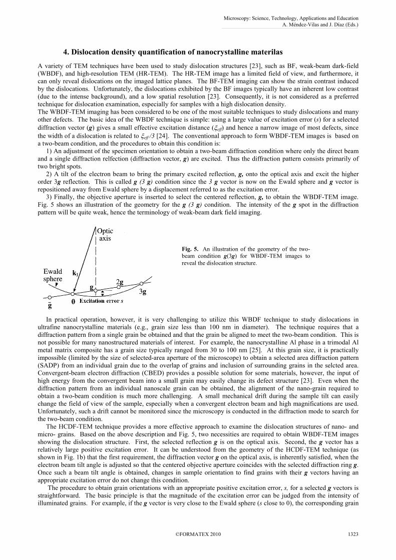
4. Dislocation density quantification of nanocrystalline materilas
A variety of TEM techniques have been used to study dislocation structures [23], such as BF, weak-beam dark-field
(WBDF), and high-resolution TEM (HR-TEM). The HR-TEM image has a limited field of view, and furthermore, it
can only reveal dislocations on the imaged lattice planes. The BF-TEM imaging can show the strain contrast induced
by the dislocations. Unfortunately, the dislocations exhibited by the BF images typically have an inherent low contrast
(due to the intense background), and a low spatial resolution [23]. Consequently, it is not considered as a preferred
technique for dislocation examination, especially for samples with a high dislocation density.
The WBDF-TEM imaging has been considered to be one of the most suitable techniques to study dislocations and many
other defects. The basic idea of the WBDF technique is simple: using a large value of excitation error (s) for a selected
diffraction vector (g) gives a small effective excitation distance (ξeff) and hence a narrow image of most defects, since
the width of a dislocation is related to ξeff /3 [24]. The conventional approach to form WBDF-TEM images is based on
a two-beam condition, and the procedures to obtain this condition is:
1) An adjustment of the specimen orientation to obtain a two-beam diffraction condition where only the direct beam
and a single diffraction relfection (diffraction vector, g) are excited. Thus the diffraction pattern consists primarily of
two bright spots.
2) A tilt of the electron beam to bring the primary excited reflection, g, onto the optical axis and excit the higher
order 3g reflection. This is called g (3 g) condition since the 3 g vector is now on the Ewald sphere and g vector is
repositioned away from Ewald sphere by a displacement referred to as the excitation error.
3) Finally, the objective aperture is inserted to select the centered reflection, g, to obtain the WBDF-TEM image.
Fig. 5 shows an illustration of the geometry for the g (3 g) condition. The intensity of the g spot in the diffraction
pattern will be quite weak, hence the terminology of weak-beam dark field imaging.
In practical operation, however, it is very challenging to utilize this WBDF technique to study dislocations in
ultrafine nanocrystalline materials (e.g., grain size less than 100 nm in diameter). The technique requires that a
diffraction pattern from a single grain be obtained and that the grain be aligned to meet the two-beam condition. This is
not possible for many nanostructured materials of interest. For example, the nanocrystalline Al phase in a trimodal Al
metal matrix composite has a grain size typically ranged from 30 to 100 nm [25]. At this grain size, it is practically
impossible (limited by the size of selected-area aperture of the microscope) to obtain a selected area diffraction pattern
(SADP) from an individual grain due to the overlap of grains and inclusion of surrounding grains in the selcted area.
Convergent-beam electron diffraction (CBED) provides a possible solution for some materials, however, the input of
high energy from the convergent beam into a small grain may easily change its defect structure [23]. Even when the
diffraction pattern from an individual nanoscale grain can be obtained, the alignment of the nano-grain required to
obtain a two-beam condition is much more challenging. A small mechanical drift during the sample tilt can easily
change the field of view of the sample, especially when a convergent electron beam and high magnifications are used.
Unfortunately, such a drift cannot be monitored since the microscopy is conducted in the diffraction mode to search for
the two-beam condition.
The HCDF-TEM technique provides a more effective approach to examine the dislocation structures of nano- and
micro- grains. Based on the above description and Fig. 5, two necessities are required to obtain WBDF-TEM images
showing the dislocation structure. First, the selected reflection g is on the optical axis. Second, the g vector has a
relatively large positive excitation error. It can be understood from the geometry of the HCDF-TEM technique (as
shown in Fig. 1b) that the first requirement, the diffraction vector g on the optical axis, is inherently satisfied, when the
electron beam tilt angle is adjusted so that the centered objective aperture coincides with the selected diffraction ring g.
Once such a beam tilt angle is obtained, changes in sample orientation to find grains with their g vectors having an
appropriate excitation error do not change this condition.
The procedure to obtain grain orientations with an appropriate positive excitation error, s, for a selected g vectors is
straightforward. The basic principle is that the magnitude of the excitation error can be judged from the intensity of
illuminated grains. For example, if the g vector is very close to the Ewald sphere (s close to 0), the corresponding grain
Fig. 5. An illustration of the geometry of the two-
beam condition g(3g) for WBDF-TEM images to
reveal the dislocation structure.
Microscopy: Science, Technology, Applications and Education A. Méndez-Vilas and J. Díaz (Eds.)
©FORMATEX 2010 1323
______________________________________________
is highly illuminated in the dark field image. On the other hand, if the vector is far away from the sphere (with a very
large s), the grain is dark in the micrograph. In theory, the grains with a moderately large s should have an intermediate
intensity, but practically, it is difficult to identify these grains simply by their intensities. Our approach is to proceed as
follows:
1) A dark field image is obtained by using a reflection (g vector) of interest. A brightly illuminated grain in the
dark field image is chosen for dislocation imagine. The highly illuminated grain can be obtained by manually rotating
the diffraction pattern and/or by tilting the samples.
2)The sample is then tilted about both axis to maximize the brightness of the chosen grain in the dark field image.
This establishes that the g vector for the grain of interst is on the Ewald sphere.
3)Whenever highly illuminated grains are obtained (i.e., s close to 0), a small tilt of the specimen can increase the
excitation error, either in a positive or negative direction, where a rotation of electron beam may be necessary when the
diffraction spot is out of the objective aperture. The image can be recorded when the grain intensity is reduced, but the
intensity may not be reduced to the extent that the defect structure is not observable. High-quality micrographs of the
dislocation structure can only be obtained if the excitation error is in a positive direction. The sign of the excitation
error can be judged by comparing the corresponding image qualities when samples are tilted in two different directions.
The image with the positive excitation error will provide dislocation contrast and can be used for measurements of
dislocation density.
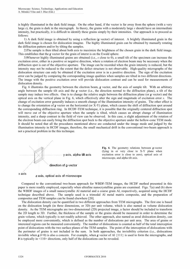
Fig. 6 illustrates the geometry between the electron beam, g vector, and the axis of sample tilt. With an arbitrary
angle between the sample tilt axis and the g vector (i.e., the direction normal to the diffraction plane), a tilt of the
sample may induce two effects. One is to change the relative angle between the diffraction plane (or g vector) and the
optical axis on the vertical plane in Fig. 6, which effectively alter the sign and magnitude of excitation error s. The
change of excitation error generally induces a smooth change of the illumination intensity of grains. The other effect is
to change the orientation of g vector on the horizontal (or X-Y) plane, which causes the shift of diffraction spot around
the corresponding diffraction ring. In HCDF-TEM technique, it is possible that the originally centered diffraction spot
will move out of the objective aperture when the sample is tilted, which causes an abrupt change of illumination
intensity, and a sharp contrast in the field of view can be observed. In this case, a slight adjustment of the rotation of
the electron beam can easily bring the diffraction spot beck to the objective aperture under the hollow-cone TEM mode.
It should be noted that all the procedures mentioned above are conducted under the image mode and judged by the
illumination intensity in HCDF images, therefore, the small mechanical drift in the conventional two-beam approach is
not a practical problem in the this technique.
Compared to the conventional two-beam approach for WBDF-TEM images, the HCDF method presented in this
paper is more readily employed, especially when ultrafine nanocrystalline grains are examined. Figs. 7(a) and (b) show
the WBDF images of a small nanocrystallie Al material and a coarse grain Al, respectively, acquired using the HCDF
technique described above. The sample used is a trimodal Al metal matrix composite, and the preparation of
composites and TEM samples can be found elsewhere [20].
The dislocation density can be quantified in two different approaches from TEM micrographs. The first one is based
on the dislocation length (in three dimensions, or 3D) per unit volume, which is also named as volume dislocation
density. As the TEM micrographs are two-dimensional (2D) projected image, a factor should be included to transform
the 2D length to 3D. Further, the thickness of the sample or the grains should be measured in order to determine the
grain volume, which typically is not readily achieved. The other approach, also named as areal dislocation density, can
be employed more conveniently, which is defined as the number of dislocations per unit area. The area of grains or
interested regions can be measured conveniently. The number of dislocations is counted as half of the total interception
point of dislocations with the two surface planes of the TEM samples. The point of the interception of dislocations with
the perimeter of grains is not included in the sum. In both approaches, the invisibility criterion (i.e., dislocations
invisible when g.b=0) is also a concern. For example, when g vector of Al {111} is used to form the micrographs, and
b is typically in <110> directions, only half of the dislocations can be revealed.
Fig. 6. The geometry relations between g-vector
(lying in or very close to X-Y plane when
excitation error is close to zero), optical axis of
microscope, and alpha tilt axis.
Microscopy: Science, Technology, Applications and Education A. Méndez-Vilas and J. Díaz (Eds.)
1324 ©FORMATEX 2010
______________________________________________

100 nm100 nm
Fig. 7. The WBDF micrographs showing the dislocation structure in (a) nanocrystalline Al phase and (b) coarse grain Al phase. The
dislocations in nanocrystalline Al phase are formed through the cryomilling, while those in coarse grain Al phase are produced by the
thermo-mechanical deformation process.
5. Conclusions
Methodologies based on HCDF-TEM are described to study grain size and dislocation density in nanocrystalline
materials. It has been demonstrated that HCDF-TEM imaging, with a slightly convergent beam, as an improved
technique was found to be suitable to form high contrast micrographs for nanocrystalline grain size quantification.
Factors which may influence the quality of HCD-TEM micrographs are also reviewed briefly. A variant geometry of
HCDF can also be used to examine dislocation structure. Compared to the conventional two-beam approach to form
WBDF-TEM images for dislocation characterization, the method described in this study is more readily applied to
provide high-quality WBDF-TEM images, and it is suitable to study both samples with coarse grains and those with
ultrafine nanocrystalline grains. Examples from both thin film and bulk nanostructured samples are presented.
Acknowledgements The grain size quantification work was supported by the Semiconductor Research Corporation, Task
1292.008. Partial support from the MRSEC program of the NSF under DMR-0520425 is also acknowledged. The dislocation study
was sponsored by U.S. Army Research Laboratory (ARL) and was accomplished under Cooperative Agreement W911NF-07-2-
0073. The views and conclusions made in this document are those of the authors and should not be interpreted as representing the
official policies, either expressed or implied, of ARL or the US Government. The US Government is authorized to reproduce and
distribute reprints for Government purposes notwithstanding any copyright notation hereon. The use of the Materials
Characterization Facility of the Advanced Materials Processing and Analysis Center at University of Central Florida is gratefully
acknowledged.
References
[1] Roco MC, Williams RS, Alivisatos P, eds. Nanotechnology research directions. Dordrecht: Kluwer; 2000.
[2] Gleiter H. Nanostructured materials: basic concepts and microstructure. Acta Materialia. 2000; 48(1): 1-29.
[3] Moriarty P. Nanostructured materials. Reports on Progress in Physics. 2001; 64: 297–381.
[4] Pande CS, Cooper KP. Nanomechanics of Hall-Petch relationship in nanocrystalline materials. Progress in Materials Science.
2009; 54: 689-706.
[5] Sun T, Yao B, Warren AP, Barmak K, Toney MF, Peale RE, Coffey KR. Surface and grain-boundary scattering in nanometric Cu
films. Physical Review B: Condensed Matter and Materials Physics. 2010; 81(15): 155454/1-155454/12.
[6] Suryanarayana C, Koch CC. Nanocrystalline materials - Current research and future directions. Hyperfine Interactions. 2001;
130(1-4): 5-44.
[7] Erdelyi Z, Langer GA, Csik A, Beke DL. Nanoscale effects in interdiffusion. Diffusion and Defect Data--Solid State Data, Pt. A:
Defect and Diffusion Forum. 2007; 264:91-98.
[8] Callister WDJ, eds. Materials Science and Engineering: An Introduction. New York: Wiley; 2007: 191-199.
[9] Liao XZ, Zhou F, Lavernia EJ, Srinivasan SG, Baskes MI, He DW, Zhu YT. Deformation mechanism in nanocrystalline Al:
partial dislocation slip. Applied Physics Letters. 2003; 83(4):632-634.
[10] Cullity BD, Stock SR. eds. Elements of X-ray Diffraction. 3rd ed. New Jersey: Pearson; 2001.
[11] Bettles CJ, Rossouw CJ. Detection of Au precipitates in a Mg-based alloy using electronically simulated hollow cone
illumination. Micron. 2000; 31(6): 651-657.
[12] Ristau RA, Hofer F, Barmak K, Coffey KR, Howard JK. An EFTEM and conical dark field investigation of co-sputtered
CoPt+yttria stabilized zirconia thin films. Micron. 1998; 29(1): 33-41.
[13] Barmak K, Darbal A, Nuhfer JT, Dingley DJ, Meaden G, Michael J, Sun T, Coffey KR. Orientation Imaging of Nanocrystalline
Platinum Films in the TEM. Proceedings of Microscopy and Microanalysis. 2009;15 Supplement 2:1232-1233.
(a) (b)
Microscopy: Science, Technology, Applications and Education A. Méndez-Vilas and J. Díaz (Eds.)
©FORMATEX 2010 1325
______________________________________________

[14] Dingley DJ, Wright SI. Crystallographic mapping in scanning electron microscopy and transmission electron microscopy with
application to semiconductor materials. 1998; Materials Research Society Symposium Proceedings. 523(Electron Microscopy
of Semiconducting Materials and ULSI Devices): 253-264.
[15] Wright SI, Dingley DJ. Orientation imaging in the transmission electron microscope. Materials Science Forum. 1998; 273-
275(Texture and Anisotropy of Polycrystals):209-214.
[16] Yao B, Coffey KR. Quantification of L0 phase volume fraction in annealed [Fe/Pt]n multilayer films. Journal of Applied Physics.
2009; 105(3): 033901/1-033901/8.
[17] Yao B, Sun T, Warren A, Heinrich H, Barmak K, Coffey KR. High contrast hollow-cone dark field transmission electron
microscopy for nanocrystalline grain size quantification. Micron. 2009; 41(3):177-182.
[18] Sun BB, Wang YB, Wen J, Yang H, Sui ML, Wang JQ, Ma E. Artifacts induced in metallic glasses during TEM sample
preparation. Scripta Materialia. 2005; 53: 805–809.
[19] Kato NI. Reducing focused ion beam damage to transmission electron microscopy samples. Journal of electron microscopy.
2004; 53: 451-458.
[20] Yao B, Coffey KR. Back-etch method for plan view transmission electron microscopy sample preparation of optically opaque
films. Journal of Electron Microscopy. 2008; 57(2): 47-52.
[21] Yao B, Petrova RV, Vanfleet RR, Coffey KR. A modified back-etch method for preparation of plan-view high-resolution
transmission electron microscopy samples. Journal of Electron Microscopy. 2006;55(4): 209-214.
[22] Carpenter DT, Rickman JM, Barmak K. A methodology for automated quantitative microstructural analysis of transmission
electron micrographs. Journal of Applied Physics. 1998; 84(11): 5843-5854.
[23] Williams DB, Carter CB, eds. Transmission Electron Microscopy, A Textbook for Materials Science. New York: Plenum; 1996:
401-481.
[24] Cockayne DJH, Ray ILF, Whelan MJ. Investigations of dislocation strain fields using weak beams. Philosophical Magazine.
1969; 20(168): 1265-70.
[25] Yao B, Hofmeister C, Patterson T, Sohn YH, van den Bergh M, Delahanty T, Cho K. Microstructural Features Influencing the
Strength of tri-modal Aluminum Metal Matrix Composites. Compsites A. 2010; in press.
Microscopy: Science, Technology, Applications and Education A. Méndez-Vilas and J. Díaz (Eds.)
1326 ©FORMATEX 2010
______________________________________________