hoja de datos
DESCRIPTION
Hoja de datos delAd633TRANSCRIPT
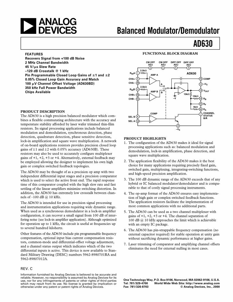
FUNCTIONAL BLOCK DIAGRAM
CM OFFADJ
CM OFFADJ
DIFF OFFADJ
DIFF OFFADJ
6 3452.5k
AMP A
2.5k
AMP B
–V
10k10k
17
5k
8
9
10
COMP
19
18
1
15
7
16
14
13
11
12
RINA
CHA+
CHA–
RINB
CHB+
CHB–
SEL B
SEL A
2
20
COMP
+VS
VOUT
RB
RF
RA
CHANNELSTATUSB/A
–VS
AD630
A
B
REV. C
Information furnished by Analog Devices is believed to be accurate andreliable. However, no responsibility is assumed by Analog Devices for itsuse, nor for any infringements of patents or other rights of third partieswhich may result from its use. No license is granted by implication orotherwise under any patent or patent rights of Analog Devices.
a Balanced Modulator/DemodulatorAD630
PRODUCT DESCRIPTIONThe AD630 is a high precision balanced modulator which com-bines a flexible commutating architecture with the accuracy andtemperature stability afforded by laser wafer trimmed thin-filmresistors. Its signal processing applications include balancedmodulation and demodulation, synchronous detection, phasedetection, quadrature detection, phase sensitive detection,lock-in amplification and square wave multiplication. A networkof on-board applications resistors provides precision closed loopgains of ±1 and ±2 with 0.05% accuracy (AD630B). Theseresistors may also be used to accurately configure multiplexergains of +1, +2, +3 or +4. Alternatively, external feedback maybe employed allowing the designer to implement his own highgain or complex switched feedback topologies.
The AD630 may be thought of as a precision op amp with twoindependent differential input stages and a precision comparatorwhich is used to select the active front end. The rapid responsetime of this comparator coupled with the high slew rate and fastsettling of the linear amplifiers minimize switching distortion. Inaddition, the AD630 has extremely low crosstalk between chan-nels of –100 dB @ 10 kHz.
The AD630 is intended for use in precision signal processingand instrumentation applications requiring wide dynamic range.When used as a synchronous demodulator in a lock-in amplifierconfiguration, it can recover a small signal from 100 dB of inter-fering noise (see lock-in amplifier application). Although optimizedfor operation up to 1 kHz, the circuit is useful at frequencies upto several hundred kilohertz.
Other features of the AD630 include pin programmable frequencycompensation, optional input bias current compensation resis-tors, common-mode and differential-offset voltage adjustment,and a channel status output which indicates which of the twodifferential inputs is active. This device is now available to Stan-dard Military Drawing (DESC) numbers 5962-8980701RA and5962-89807012A.
PRODUCT HIGHLIGHTS1. The configuration of the AD630 makes it ideal for signal
processing applications such as: balanced modulation anddemodulation, lock-in amplification, phase detection, andsquare wave multiplication.
2. The application flexibility of the AD630 makes it the bestchoice for many applications requiring precisely fixed gain,switched gain, multiplexing, integrating-switching functions,and high-speed precision amplification.
3. The 100 dB dynamic range of the AD630 exceeds that of anyhybrid or IC balanced modulator/demodulator and is compa-rable to that of costly signal processing instruments.
4. The op-amp format of the AD630 ensures easy implementa-tion of high gain or complex switched feedback functions.The application resistors facilitate the implementation ofmost common applications with no additional parts.
5. The AD630 can be used as a two channel multiplexer withgains of +1, +2, +3 or +4. The channel separation of100 dB @ 10 kHz approaches the limit which is achievablewith an empty IC package.
6. The AD630 has pin-strappable frequency compensation (noexternal capacitor required) for stable operation at unity gainwithout sacrificing dynamic performance at higher gains.
7. Laser trimming of comparator and amplifying channel offsetseliminates the need for external nulling in most cases.
FEATURES
Recovers Signal from +100 dB Noise
2 MHz Channel Bandwidth
45 V/s Slew Rate
–120 dB Crosstalk @ 1 kHz
Pin Programmable Closed Loop Gains of 1 and 2
0.05% Closed Loop Gain Accuracy and Match
100 V Channel Offset Voltage (AD630BD)
350 kHz Full Power Bandwidth
Chips Available
One Technology Way, P.O. Box 9106, Norwood, MA 02062-9106, U.S.A.
Tel: 781/329-4700 World Wide Web Site: http://www.analog.com
Fax: 781/326-8703 © Analog Devices, Inc., 2000
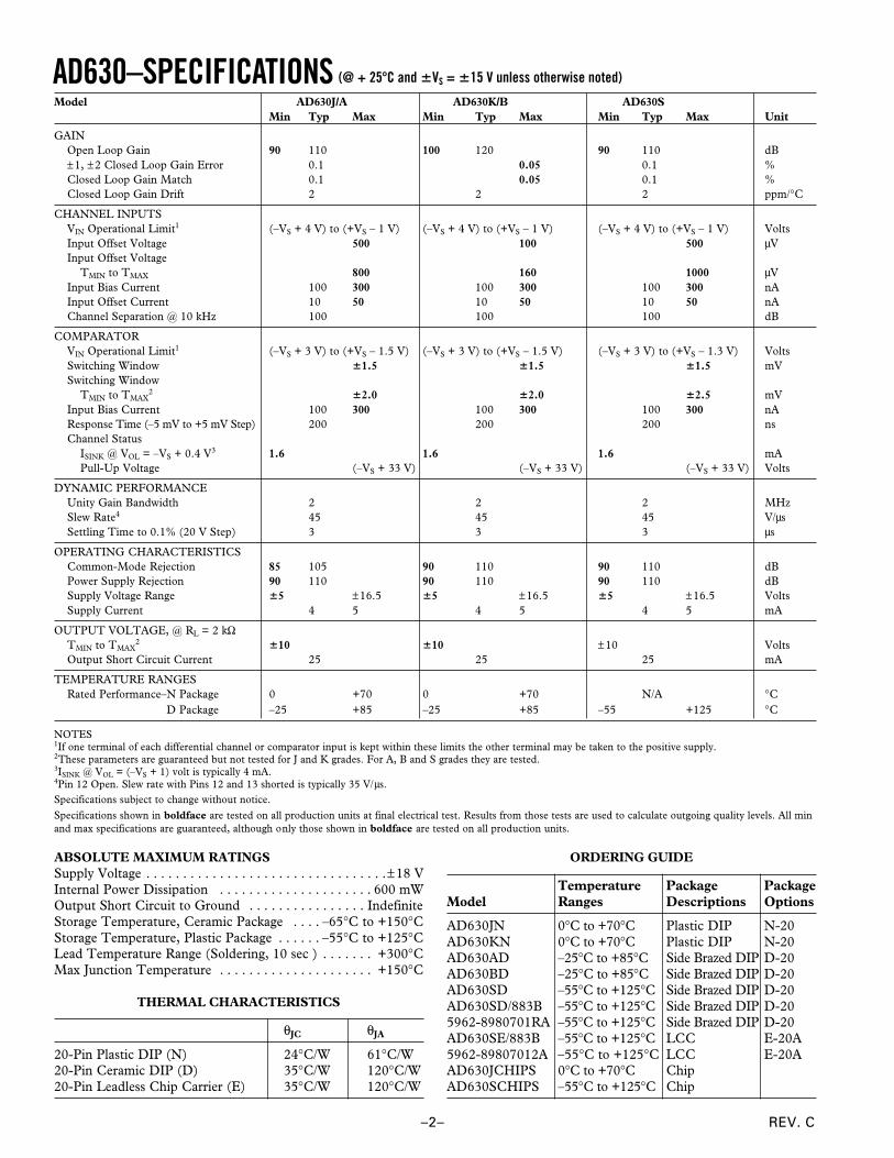
AD630–SPECIFICATIONS
REV. C–2–
ORDERING GUIDE
Temperature Package PackageModel Ranges Descriptions Options
AD630JN 0°C to +70°C Plastic DIP N-20AD630KN 0°C to +70°C Plastic DIP N-20AD630AD –25°C to +85°C Side Brazed DIP D-20AD630BD –25°C to +85°C Side Brazed DIP D-20AD630SD –55°C to +125°C Side Brazed DIP D-20AD630SD/883B –55°C to +125°C Side Brazed DIP D-205962-8980701RA –55°C to +125°C Side Brazed DIP D-20AD630SE/883B –55°C to +125°C LCC E-20A5962-89807012A –55°C to +125°C LCC E-20AAD630JCHIPS 0°C to +70°C ChipAD630SCHIPS –55°C to +125°C Chip
(@ + 25C and VS = 15 V unless otherwise noted)
Model AD630J/A AD630K/B AD630SMin Typ Max Min Typ Max Min Typ Max Unit
GAINOpen Loop Gain 90 110 100 120 90 110 dB±1, ±2 Closed Loop Gain Error 0.1 0.05 0.1 %Closed Loop Gain Match 0.1 0.05 0.1 %Closed Loop Gain Drift 2 2 2 ppm/°C
CHANNEL INPUTSVIN Operational Limit1 (–VS + 4 V) to (+VS – 1 V) (–VS + 4 V) to (+VS – 1 V) (–VS + 4 V) to (+VS – 1 V) VoltsInput Offset Voltage 500 100 500 µVInput Offset Voltage
TMIN to TMAX 800 160 1000 µVInput Bias Current 100 300 100 300 100 300 nAInput Offset Current 10 50 10 50 10 50 nAChannel Separation @ 10 kHz 100 100 100 dB
COMPARATORVIN Operational Limit1 (–VS + 3 V) to (+VS – 1.5 V) (–VS + 3 V) to (+VS – 1.5 V) (–VS + 3 V) to (+VS – 1.3 V) VoltsSwitching Window 1.5 1.5 1.5 mVSwitching Window
TMIN to TMAX2 2.0 2.0 2.5 mV
Input Bias Current 100 300 100 300 100 300 nAResponse Time (–5 mV to +5 mV Step) 200 200 200 nsChannel Status
ISINK @ VOL = –VS + 0.4 V3 1.6 1.6 1.6 mAPull-Up Voltage (–VS + 33 V) (–VS + 33 V) (–VS + 33 V) Volts
DYNAMIC PERFORMANCEUnity Gain Bandwidth 2 2 2 MHzSlew Rate4 45 45 45 V/µsSettling Time to 0.1% (20 V Step) 3 3 3 µs
OPERATING CHARACTERISTICSCommon-Mode Rejection 85 105 90 110 90 110 dBPower Supply Rejection 90 110 90 110 90 110 dBSupply Voltage Range 5 ±16.5 5 ±16.5 5 ±16.5 VoltsSupply Current 4 5 4 5 4 5 mA
OUTPUT VOLTAGE, @ RL = 2 kΩTMIN to TMAX
2 10 10 ±10 VoltsOutput Short Circuit Current 25 25 25 mA
TEMPERATURE RANGESRated Performance–N Package 0 +70 0 +70 N/A °CRated Performance–D Package –25 +85 –25 +85 –55 +125 °C
NOTES1If one terminal of each differential channel or comparator input is kept within these limits the other terminal may be taken to the positive supply.2These parameters are guaranteed but not tested for J and K grades. For A, B and S grades they are tested.3ISINK @ VOL = (–VS + 1) volt is typically 4 mA.4Pin 12 Open. Slew rate with Pins 12 and 13 shorted is typically 35 V/µs.Specifications subject to change without notice.Specifications shown in boldface are tested on all production units at final electrical test. Results from those tests are used to calculate outgoing quality levels. All minand max specifications are guaranteed, although only those shown in boldface are tested on all production units.
ABSOLUTE MAXIMUM RATINGSSupply Voltage . . . . . . . . . . . . . . . . . . . . . . . . . . . . . . . . .±18 VInternal Power Dissipation . . . . . . . . . . . . . . . . . . . . . 600 mWOutput Short Circuit to Ground . . . . . . . . . . . . . . . . IndefiniteStorage Temperature, Ceramic Package . . . . –65°C to +150°CStorage Temperature, Plastic Package . . . . . . –55°C to +125°CLead Temperature Range (Soldering, 10 sec ) . . . . . . . +300°CMax Junction Temperature . . . . . . . . . . . . . . . . . . . . . +150°C
THERMAL CHARACTERISTICS
θJC θJA
20-Pin Plastic DIP (N) 24°C/W 61°C/W20-Pin Ceramic DIP (D) 35°C/W 120°C/W20-Pin Leadless Chip Carrier (E) 35°C/W 120°C/W
AD630
REV. C –3–
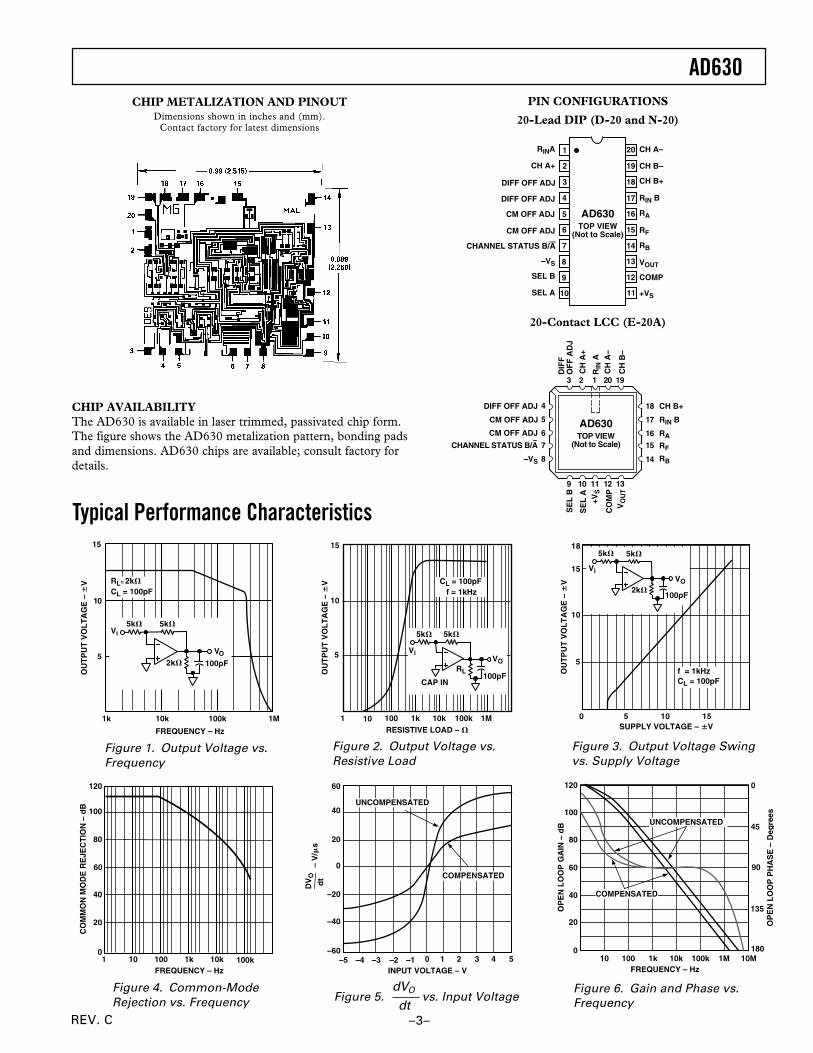
PIN CONFIGURATIONS
20-Lead DIP (D-20 and N-20)
14
13
12
11
17
16
15
20
19
18
10
9
8
1
2
3
4
7
6
5
TOP VIEW(Not to Scale)
AD630
RINA
RIN B
CH B+
CH B–
CH A–
CH A+
DIFF OFF ADJ
DIFF OFF ADJ
RB
RF
RACM OFF ADJ
CM OFF ADJ
–VS
SEL B
SEL A +VS
COMP
VOUT
CHANNEL STATUS B/A
20-Contact LCC (E-20A)
20 19123
18
14
15
16
17
4
5
6
7
8
9 10 11 12 13
TOP VIEW(Not to Scale)
AD630
DIFF OFF ADJ
CM OFF ADJ
CM OFF ADJ
CHANNEL STATUS B/A
–VS
CH B+
RIN B
RA
RF
RB
DIF
FO
FF
AD
J
CH
A+
RIN
AC
H A
–
CH
B–
SE
L B
SE
L A
+VS
CO
MP
VO
UT
Typical Performance Characteristics
Figure 2. Output Voltage vs.Resistive Load
Figure 3. Output Voltage Swingvs. Supply Voltage
Figure 4. Common-ModeRejection vs. Frequency Figure 5.
dVO
dtvs. Input Voltage
Figure 6. Gain and Phase vs.Frequency
CHIP METALIZATION AND PINOUTDimensions shown in inches and (mm).
Contact factory for latest dimensions
CHIP AVAILABILITYThe AD630 is available in laser trimmed, passivated chip form.The figure shows the AD630 metalization pattern, bonding padsand dimensions. AD630 chips are available; consult factory fordetails.
Figure 1. Output Voltage vs.Frequency
FREQUENCY – Hz
15
10
5
1k 10k 1M100k
RL= 2k
CL = 100pF
2k
5k5kVi
VO
100pF
OU
TP
UT
VO
LT
AG
E –
V
10
15
5
1 10 100 1k 10k 100k 1MRESISTIVE LOAD –
CL = 100pF f = 1kHz
CAP IN
5k
VO
100pFRL
Vi
5k
OU
TP
UT
VO
LT
AG
E –
V
10
18
5
0 5 10 15SUPPLY VOLTAGE – V
OU
TP
UT
VO
LT
AG
E –
V
15
5k
100pF
Vi
5k
2k
VO
f = 1kHz CL = 100pF
FREQUENCY – Hz
CO
MM
ON
MO
DE
RE
JEC
TIO
N –
dB
120
60
01 10 100k100 1k 10k
100
80
40
20
INPUT VOLTAGE – V
DV
O
dt
– V
/s
60
0
–60–5 –3 4–2 –1 1
40
20
–40
–20
–4 0 2 3 5
UNCOMPENSATED
COMPENSATED
FREQUENCY – Hz
120
60
01M100
100
80
20
40
10 1k 100k10k
UNCOMPENSATED
10M
0
45
90
OP
EN
LO
OP
GA
IN –
dB
135
180
COMPENSATED
OP
EN
LO
OP
PH
AS
E –
Deg
rees
REV. C–4–
AD630–Typical Performance Characteristics
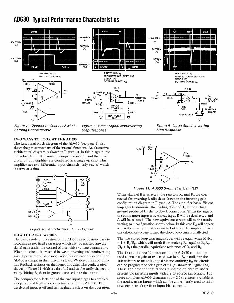
Figure 7. Channel-to-Channel Switch-Settling Characteristic
Figure 9. Large Signal InvertingStep Response
TWO WAYS TO LOOK AT THE AD630The functional block diagram of the AD630 (see page 1) alsoshows the pin connections of the internal functions. An alternativearchitectural diagram is shown in Figure 10. In this diagram, theindividual A and B channel preamps, the switch, and the inte-grator output amplifier are combined in a single op amp. Thisamplifier has two differential input channels, only one of whichis active at a time.
1115
2
20
19
18
17
8
7
12
14
13
9
10
RA 5k
2.5k
RF10k
1
16
2.5k
+VS
RB10k
SEL B
SEL A
B/A
A
B
–VS
Figure 10. Architectural Block Diagram
HOW THE AD630 WORKSThe basic mode of operation of the AD630 may be more easy torecognize as two fixed gain stages which may be inserted into thesignal path under the control of a sensitive voltage comparator.When the circuit is switched between inverting and noninvertinggain, it provides the basic modulation/demodulation function. TheAD630 is unique in that it includes Laser-Wafer-Trimmed thin-film feedback resistors on the monolithic chip. The configurationshown in Figure 11 yields a gain of ±2 and can be easily changed to±1 by shifting RB from its ground connection to the output.
The comparator selects one of the two input stages to completean operational feedback connection around the AD630. Thedeselected input is off and has negligible effect on the operation.
A
B
RA5k
RF10k
VO
RB10k
Vi
2
20
19
1813
1516
149
10
Figure 11. AD630 Symmetric Gain (±2)
When channel B is selected, the resistors RA and RF are con-nected for inverting feedback as shown in the inverting gainconfiguration diagram in Figure 12. The amplifier has sufficientloop gain to minimize the loading effect of RB at the virtualground produced by the feedback connection. When the sign ofthe comparator input is reversed, input B will be deselected andA will be selected. The new equivalent circuit will be the nonin-verting gain configuration shown below. In this case RA will appearacross the op-amp input terminals, but since the amplifier drivesthis difference voltage to zero the closed loop gain is unaffected.
The two closed loop gain magnitudes will be equal when RF/RA
= 1 + RF/RB, which will result from making RA equal to RFRB/(RF + RB) the parallel equivalent resistance of RF and RB.
The 5k and the two 10k resistors on the AD630 chip can beused to make a gain of two as shown here. By paralleling the10k resistors to make RF equal 5k and omitting RB the circuitcan be programmed for a gain of ±1 (as shown in Figure 18a).These and other configurations using the on chip resistorspresent the inverting inputs with a 2.5k source impedance. Themore complete AD630 diagrams show 2.5k resistors available atthe noninverting inputs which can be conveniently used to mini-mize errors resulting from input bias currents.
Figure 8. Small Signal NoninvertingStep Response
20mV 500ns
20mV
100
90
10
0%
20mV/DIV(Vo)
20mV/DIV(Vi)
TOP TRACE: VoBOTTOM TRACE: Vi
100
90
10
0%
100mV 500ns
50mV 1mV
50mV/DIV(Vi)
1mV/DIV(A)
TOP TRACE: ViMIDDLE TRACE: SETTLINGERROR (A)BOTTOM TRACE: Vo
100mV/DIV(Vo)
100
90
10
0%
10V
10V 1mV
TOP TRACE: ViMIDDLE TRACE: SETTLINGERROR (B)BOTTOM TRACE: Vo
5s
10V 20kHz(Vi)
1mV/DIV(B)
10V/DIV(Vo)
5k 10k
10k
Vi
CHA
CHB
12
VO
2
20
19
18
13
9
10
14
16 15
12CH A
MIDDLETRACE
(A)
10k
10k
VOBOTTOMTRACE
TEKTRONIX7A13
10k
1k
30pF
10k
ViTOP
TRACE
2
2013
14 15
12CH A
10k
10k
VOBOTTOMTRACE
10k
ViTOP
TRACE
(B)MIDDLETRACE
10k
HP5082-2811
20
213
14 15

AD630
REV. C –5–
RA5k
RF 10k
RB10k
Vi
VO = –RF
RAVi
Figure 12. Inverting Gain Configuration
RA5k
RF10k
RB10k
Vi
VO = (1+RF
RB) Vi
Figure 13. Noninverting Gain Configuration
CIRCUIT DESCRIPTIONThe simplified schematic of the AD630 is shown in Figure 14.It has been subdivided into three major sections, the comparator,the two input stages and the output integrator. The comparatorconsists of a front end made up of Q52 and Q53, a flip-flop loadformed by Q3 and Q4, and two current steering switching cellsQ28, Q29 and Q30, Q31. This structure is designed so that adifferential input voltage greater than 1.5 mV in magnitudeapplied to the comparator inputs will completely select one theswitching cells. The sign of this input voltage determine whichof the two switching cells is selected.
20
11
3 4 5 6
192 18
13
12
SEL A
SEL B
DIFFOFF ADJ
DIFFOFF ADJ
CMOFF ADJ
CMOFF ADJ
COMP
Q74
Q44
CH B–CH B+CH A+CH A–
i55
Q4Q3
Q28Q31
Q30
Q32C122
C121
i22 i23
–VS
VO
i73
Q52 Q53
+VS
Q65
Q34Q33
Q62
Q35 Q36
Q67 Q70
Q25Q24Q29
10
9
8
Figure 14. AD630 Simplified Schematic
The collectors of each switching cell connect to an input trans-conductance stage. The selected cell conveys bias currents i22
and i23 to the input stage it controls, causing it to become active.The deselected cell blocks the bias to its input stage which, as aconsequence, remains off.
The structure of the transconductance stages is such that theypresent a high impedance at their input terminals and draw nobias current when deselected. The deselected input does notinterfere with the operation of the selected input insuring maxi-mum channel separation.
Another feature of the input structure is that it enhances theslew rate of the circuit. The current output of the active stagefollows a quasi-hyperbolic-sine relationship to the differentialinput voltage. This means that the greater the input voltage, theharder this stage will drive the output integrator, and hence, the
faster the output signal will move. This feature helps insurerapid, symmetric settling when switching between inverting andnoninverting closed loop configurations.
The output section of the AD630 includes a current mirror-load(Q24 and Q25), an integrator-voltage gain stage (Q32), andcomplementary output buffer (Q44 and Q74). The outputs ofboth transconductance stages are connected in parallel to thecurrent mirror. Since the deselected input stage produces nooutput current and presents a high impedance at its outputs,there is no conflict. The current mirror translates the differentialoutput current from the active input transconductance amplifierinto single ended form for the output integrator. The comple-mentary output driver then buffers the integrator output pro-duce a low impedance output.
OTHER GAIN CONFIGURATIONSMany applications require switched gains other than the ±1 and±2 which the self-contained applications resistors provide. TheAD630 can be readily programmed with three external resistorsover a wide range of positive and negative gain by selecting andRB and RF to give the noninverting gain 1 + RF/RB and subsequentRA to give the desired inverting gain. Note that when the invertingmagnitude equals the noninverting magnitude, the value of RA isfound to be RB RF/(RB + RF). That is, RA should equal the parallelcombination of RB and RF to match positive and negative gain.
The feedback synthesis of the AD630 may also include reactiveimpedance. The gain magnitudes will match at all frequencies ifthe A impedance is made to equal the parallel combination ofthe B and F impedances. Essentially the same considerationsapply to the AD630 as to conventional op-amp feedback circuits.Virtually any function which can be realized with simple nonin-verting “L network” feedback can be used with the AD630. Acommon arrangement is shown in Figure 15. The low frequencygain of this circuit is 10. The response will have a pole (–3 dB)at a frequency f 1/(2 π 100 kΩC) and a zero (3 dB from thehigh frequency asymptote) at about 10 times this frequency.The 2k resistor in series with each capacitor mitigates the load-ing effect on circuitry driving this circuit, eliminates stabilityproblems, and has a minor effect on the pole-zero locations.
As a result of the reactive feedback, the high frequency componentsof the switched input signal will be transmitted at unity gain
C
–VS
A
B
10k
VO
11.11k12
Vi
100k
2k C2k
2
20
19
18
13
7
8
9
10
Figure 15. AD630 with External Feedback
while the low frequency components will be amplified. Thisarrangement is useful in demodulators and lock-in amplifiers. Itincreases the circuit dynamic range when the modulation orinterference is substantially larger than the desired signal ampli-tude. The output signal will contain the desired signal multi-plied by the low frequency gain (which may be several hundredfor large feedback ratios) with the switching signal and interfer-ence superimposed at unity gain.
REV. C–6–
AD630SWITCHED INPUT IMPEDANCEThe noninverting mode of operation is a high input impedanceconfiguration while the inverting mode is a low input impedanceconfiguration. This means that the input impedance of thecircuit undergoes an abrupt change as the gain is switched un-der control of the comparator. If gain is switched when theinput signal is not zero, as it is in many practical cases, a tran-sient will be delivered to the circuitry driving the AD630. Inmost applications, this will require the AD630 circuit to bedriven by a low impedance source which remains “stiff “ at highfrequencies. Generally this will be a wideband buffer amplifier.
FREQUENCY COMPENSATIONThe AD630 combines the convenience of internal frequencycompensation with the flexibility of external compensation bymeans of an optional self-contained compensation capacitor.
In gain of ±2 applications the noise gain which must be addressedfor stability purposes is actually 4. In this circumstance, thephase margin of the loop will be on the order of 60° without theoptional compensation. This condition provides the maximumbandwidth and slew-rate for closed-loop gains of |2| and above.
When the AD630 is used as a multiplexer, or in other configura-tions where one or both inputs are connected for unity gainfeedback, the phase margin will be reduced to less than 20°.This may be acceptable in applications where fast slewing is afirst priority, but the transient response will not be optimum.For these applications, the self-contained compensation capaci-tor may be added by connecting Pin 12 to Pin 13. This connec-tion reduces the closed loop bandwidth somewhat, and improvesthe phase margin.
For intermediate conditions, such as gain of ±1 where loopattenuation is 2, use of the compensation should be determinedby whether bandwidth or settling response must be optimized.The optional compensation should also be used when the AD630is driving capacitive loads or whenever conservative frequencycompensation is desired.
OFFSET VOLTAGE NULLINGThe offset voltages of both input stages and the comparatorhave been pretrimmed so that external trimming will only berequired in the most demanding applications. The offset adjust-ment of the two input channels is accomplished by means of adifferential and common-mode scheme. This facilitates fineadjustment of system errors in switched gain applications. Withsystem input tied to 0 V, and a switching or carrier waveformapplied to the comparator, a low level square wave will appear atthe output. The differential offset adjustment pot can be usedto null the amplitude of this square wave (Pins 3 and 4). Thecommon-mode offset adjustment can be used to zero the re-sidual dc output voltage (Pins 5 and 6). These functions shouldbe implemented using 10k trim pots with wipers connecteddirectly to Pin 8 as shown in Figures 18a and 18b.
CHANNEL STATUS OUTPUTThe channel status output, Pin 7, is an open collector outputreferenced to –VS which can be used to indicate which of thetwo input channels is active. The output will be active (pulledlow) when Channel A is selected. This output can also be usedto supply positive feedback around the comparator. This pro-duces hysteresis which serves to increase noise immunity. Figure16 shows an example of how hysteresis may be implemented.Note that the feedback signal is applied to the inverting (–)terminal of the comparator to achieve positive feedback. This is
because the open collector channel status output inverts theoutput sense of the internal comparator.
1M
100k
100k
–15V
+5V
100
7
8
9
10
Figure 16. Comparator Hysteresis
The channel status output may be interfaced with TTL inputsas shown in Figure 17. This circuit provides appropriate levelshifting from the open-collector AD630 channel status output toTTL inputs.
–15V
+5V
TTL INPUTAD630
+15V
IN 914's
6.8k22k
100k
2N22227
8
Figure 17. Channel Status—TTL Interface
APPLICATIONS: BALANCED MODULATORPerhaps the most commonly used configuration of the AD630 isthe balanced modulator. The application resistors provide pre-cise symmetric gains of ±1 and ±2. The ±1 arrangement isshown in Figure 18a and the ±2 arrangement is shown in Figure18b. These cases differ only in the connection of the 10k feed-back resistor (Pin 14) and the compensation capacitor (Pin 12).Note the use of the 2.5 kΩ bias current compensation resistorsin these examples. These resistors perform the identical functionin the ±1 gain case. Figure 19 demonstrates the performance ofthe AD630 when used to modulate a 100 kHz square wavecarrier with a 10 kHz sinusoid. The result is the double side-band suppressed carrier waveform.
These balanced modulator topologies accept two inputs, a signal(or modulation) input applied to the amplifying channels, and areference (or carrier) input applied to the comparator.
MODULATEDOUTPUTSIGNAL
CARRIERINPUT
CMADJ
DIFFADJ
2.5k
AMP A
AMP B
–V
10k
10k
5k
9
10
COMP
1
15
7
16
14
13
122
20+VS
–VS
AD630
A
B2.5k
19
18
17
11
8
6 5
10k
4 3
10k
MODULATIONINPUT
Figure 18a. AD630 Configured as a Gain-of-One BalancedModulator

AD630
REV. C –7–
MODULATEDOUTPUTSIGNAL
CARRIERINPUT
CMADJ
DIFFADJ
2.5k
AMP A
AMP B
–V
10k
10k
5k
9
10
COMP
1
15
7
16
14
13
122
20+VS
–VS
AD630
A
B2.5k
19
18
17
11
8
6 5
10k
4 3
10k
MODULATIONINPUT
Figure 18b. AD630 Configured as a Gain-of-Two BalancedModulator
10V
5V 5V 20s
MODULATIONINPUT
CARRIERINPUT
OUTPUTSIGNAL
Figure 19. Gain-of-Two Balanced Modulator SampleWaveforms
BALANCED DEMODULATORThe balanced modulator topology described above will also act asa balanced demodulator if a double sideband suppressed carrierwaveform is applied to the signal input and the carrier signal isapplied to the reference input. The output under these circum-stances will be the baseband modulation signal. Higher ordercarrier components will also be present which can be removedwith a low-pass filter. Other names for this function are synchro-nous demodulation and phase-sensitive detection.
PRECISION PHASE COMPARATORThe balanced modulator topologies of Figures 18a and 18b canalso be used as precision phase comparators. In this case, an acwaveform of a particular frequency is applied to the signal inputand a waveform of the same frequency is applied to the refer-ence input. The dc level of the output (obtained by low-passfiltering) will be proportional to the signal amplitude and phasedifference between the input signals. If the signal amplitude isheld constant, then the output can be used as a direct indicationof the phase. When these input signals are 90° out of phase, theyare said to be in quadrature and the AD630 dc output will be zero.
PRECISION RECTIFIER-ABSOLUTE VALUEIf the input signal is used as its own reference in the balancedmodulator topologies, the AD630 will act as a precision recti-fier. The high frequency performance will be superior to thatwhich can be achieved with diode feedback and op amps. Thereare no diode drops which the op amp must “leap over” with thecommutating amplifier.
LVDT SIGNAL CONDITIONERMany transducers function by modulating an ac carrier. A Lin-ear Variable Differential Transformer (LVDT) is a transducer ofthis type. The amplitude of the output signal corresponds tocore displacement. Figure 20 shows an accurate synchronousdemodulation system which can be used to produce a dc voltagewhich corresponds to the LVDT core position. The inherentprecision and temperature stability of the AD630 reduce de-modulator drift to a second order effect.
A
B
10k
10k
5k
2.5k
2.5k
C 100kD
1F
AD6302 DEMODULATOR
AD544FOLLOWER
B
PHASESHIFTER
A
E1000SCHAEVITZ
LVDT
2.5kHZ
2V p-pSINUSOIDALEXCITATION
16
1
14
17
9
10
20
1912
13
15
Figure 20. LVDT Signal Conditioner
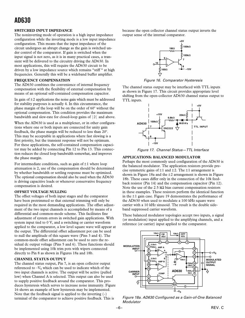
AC BRIDGEBridge circuits which use dc excitation are often plagued byerrors caused by thermocouple effects, 1/f noise, dc drifts in theelectronics, and line noise pick-up. One way to get around theseproblems is to excite the bridge with an ac waveform, amplifythe bridge output with an ac amplifier, and synchronously de-modulate the resulting signal. The ac phase and amplitudeinformation from the bridge is recovered as a dc signal at theoutput of the synchronous demodulator. The low frequencysystem noise, dc drifts, and demodulator noise all get mixed tothe carrier frequency and can be removed by means of a low-passfilter. Dynamic response of the bridge must be traded off againstthe amount of attenuation required to adequately suppress theseresidual carrier components in the selection of the filter.
Figure 21 is an example of an ac bridge system with the AD630used as a synchronous demodulator. The oscilloscope photo-graph shows the results of a 0.05% bridge imbalance caused bythe 1 Meg resistor in parallel with one leg of the bridge. The toptrace represents the bridge excitation, the upper-middle trace isthe amplified bridge output, the lower-middle trace is the out-put of the synchronous demodulator and the bottom trace is thefiltered dc system output.
This system can easily resolve a 0.5 ppm change in bridge im-pedance. Such a change will produce a 3.2 mV change in thelow-pass filtered dc output, well above the RTO drifts and noise.
1M1k
1k
1k
1k
B
A
B
A
5k 10k
10k
2.5k
2.5k
C
D5k 5k 5k
FILTER
2F
20
213
12
AD524GAIN 1000
1
AD6302 DEMODULATOR
1kHzBRIDGE
EXCITATION
PHASESHIFTER
2F2F
16
15
17
149
10
Figure 21. AC Bridge System
REV. C–8–
AD630
C00
784–
0–6/
00 (
rev.
C)
PR
INT
ED
IN U
.S.A
.
OUTLINE DIMENSIONSDimensions shown in inches and (mm).
20-Lead Ceramic DIP (D-20)
20-Lead Plastic DIP (N-20)
LCC (E-20A)
0.358(9.09)MAXSQ
0.088 (2.24)0.054 (1.37)
0.100 (2.54)0.064 (1.63)
0.358 (9.09)0.342 (8.69)
SQ
0.075(1.91)
REF
0.075(1.91)
REF
0.011 (0.28)0.007 (0.18)
R TYP
BOTTOMVIEW
0.015 (0.38)MIN
1
20
13 9
0.028 (0.71)0.022 (0.56)A
AAAAA AA
AAAAAAAAAA
0.095 (2.41)0.075 (1.90)
0.200 (5.08)BSC
0.100(2.54)BSC
0.055 (1.40)0.045 (1.14)
45°TYP
0.150(3.81)BSC
0.050(1.27)BSC
100
90
10
0%
5V
20V 5V 200s
2V
0V
0V
0V
0V
BRIDGE EXCITATION(20V/DIV) (A)
AMPLIFIED BRIDGEOUTPUT (5V/DIV) (B)
DEMODULATED BRIDGEOUTPUT (5V/DIV) (C)
FILTER OUTPUT (2V/DIV) (D)
Figure 22. AC Bridge Waveforms
LOCK-IN AMPLIFIER APPLICATIONSLock-in amplification is a technique which is used to separate asmall, narrow band signal from interfering noise. The lock-inamplifiers acts as a detector and narrow band filter combined.Very small signals can be detected in the presence of largeamounts of uncorrelated noise when the frequency and phase ofthe desired signal are known.
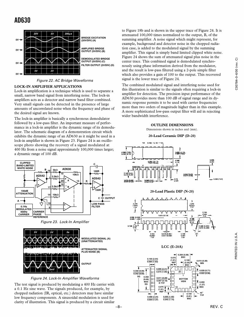
The lock-in amplifier is basically a synchronous demodulatorfollowed by a low-pass filter. An important measure of perfor-mance in a lock-in amplifier is the dynamic range of its demodu-lator. The schematic diagram of a demonstration circuit whichexhibits the dynamic range of an AD630 as it might be used in alock-in amplifier is shown in Figure 23. Figure 24 is an oscillo-scope photo showing the recovery of a signal modulated at400 Hz from a noise signal approximately 100,000 times larger;a dynamic range of 100 dB.
A
B
10k
100R
C OUTPUT
LOW PASSFILTER
A
B
C
R
100RAD630
10k
5k
2.5k
2.5k
2019
17
1
16
AD54213
AD542
14
10
9
CLIPPEDBAND-LIMITEDWHITE NOISE
100dBATTENUATION
0.1HzMODULATED
400HzCARRIER
CARRIERPHASEREFERENCE
15
Figure 23. Lock-In Amplifier
100
90
10
0%
5V 5V 5s
5mV
MODULATED SIGNAL (A)(UNATTENUATED)
ATTENUATED SIGNALPLUS NOISE (B)
OUTPUT
Figure 24. Lock-In Amplifier Waveforms
The test signal is produced by modulating a 400 Hz carrier witha 0.1 Hz sine wave. The signals produced, for example, bychopped radiation (IR, optical, etc.) detectors may have similarlow frequency components. A sinusoidal modulation is used forclarity of illustration. This signal is produced by a circuit similar
to Figure 18b and is shown in the upper trace of Figure 24. It isattenuated 100,000 times normalized to the output, B, of thesumming amplifier. A noise signal which might represent, forexample, background and detector noise in the chopped radia-tion case, is added to the modulated signal by the summingamplifier. This signal is simply band limited clipped white noise.Figure 24 shows the sum of attenuated signal plus noise in thecenter trace. This combined signal is demodulated synchro-nously using phase information derived from the modulator,and the result is low-pass filtered using a 2-pole simple filterwhich also provides a gain of 100 to the output. This recoveredsignal is the lower trace of Figure 24.
The combined modulated signal and interfering noise used forthis illustration is similar to the signals often requiring a lock-inamplifier for detection. The precision input performance of theAD630 provides more than 100 dB of signal range and its dy-namic response permits it to be used with carrier frequenciesmore than two orders of magnitude higher than in this example.A more sophisticated low-pass output filter will aid in rejectingwider bandwidth interference.