hkmg leading edge technologies -...
TRANSCRIPT
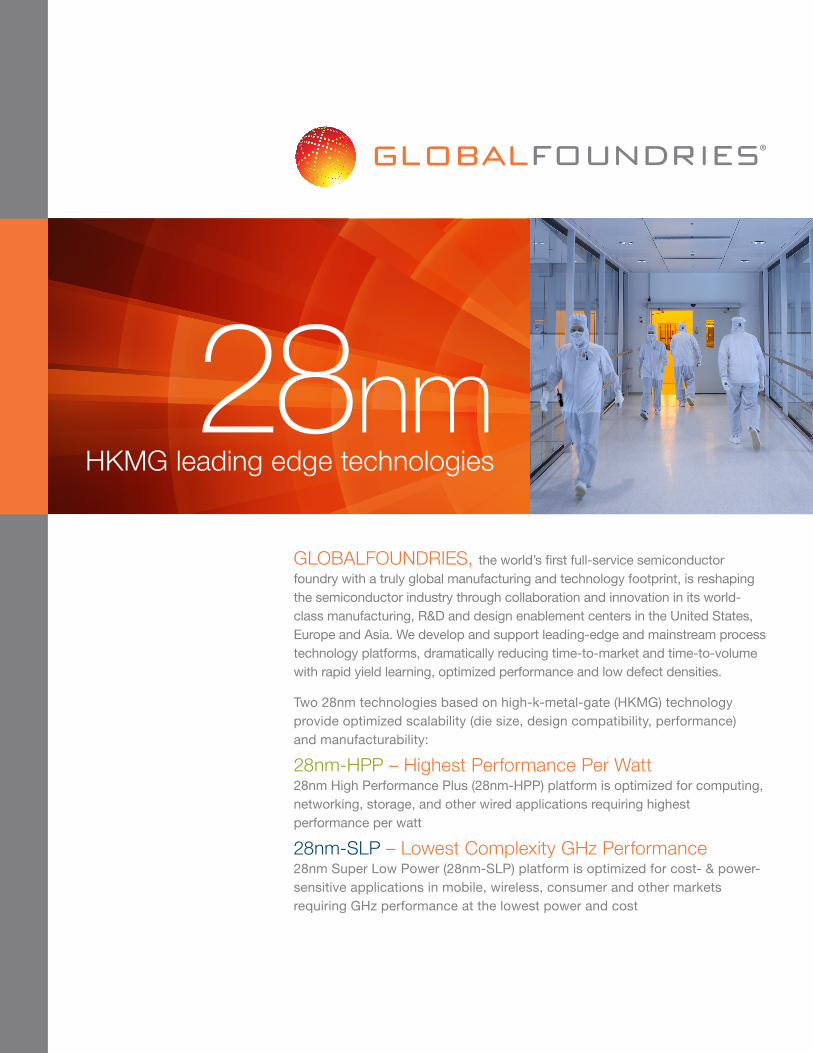
GLOBALFOUNDRIES, the world’s first full-service semiconductor foundry with a truly global manufacturing and technology footprint, is reshaping the semiconductor industry through collaboration and innovation in its world-class manufacturing, R&D and design enablement centers in the United States, Europe and Asia. We develop and support leading-edge and mainstream process technology platforms, dramatically reducing time-to-market and time-to-volume with rapid yield learning, optimized performance and low defect densities.
Two 28nm technologies based on high-k-metal-gate (HKMG) technology provide optimized scalability (die size, design compatibility, performance) and manufacturability:
28nm-HPP – Highest Performance Per Watt28nm High Performance Plus (28nm-HPP) platform is optimized for computing, networking, storage, and other wired applications requiring highest performance per watt
28nm-SLP – Lowest Complexity GHz Performance28nm Super Low Power (28nm-SLP) platform is optimized for cost- & power-sensitive applications in mobile, wireless, consumer and other markets requiring GHz performance at the lowest power and cost
28nmHKMG leading edge technologies

40LP 28SLP
40LP
28SLP
Frequency (AU x Hz)
40G
28HPP
Frequency (AU x Hz) 40G 28HPP
Optimized 28nm PlatformsGLOBALFOUNDRIES 28nm platforms offer superior Performance, Power, Area and Cost (PPAC) characteristics optimized for a wide range of applications from power-critical mobile, wireless and consumer to high-performance computing, networking and storage.
28nm-HPP and 28nm-SLP utilize High-k Metal Gate (HKMG) “Gate First” technology with superior control of the channel for high on currents and low leakage current. Both provide twice the gate density of comparable 40nm processes and an SRAM cell size shrink greater than 50 percent.
Superior Performance, Power, Area28nm-HPP and 28nm-SLP versus comparable 40/45nm platforms:
“Gate First” High-k Metal Gate (HKMG) Technology Advantages
1 Similar architecture and design rules maintained, avoiding design time and density penalties from restrictive design rules for “Gate Last” approach
Lower cost for 28nm-SLP versus “Gate Last” approach due to:
• Mask adders
• Area overhead for power management
• Area scaling disadvan-tage of gate last
Better performance/watt for 28nm-HPP due to lower voltage process
• Higher performance
• Lower power
• Area scaling disadvan-tage of gate last
2 3
Area
HPP
SLP
PowerPerformance
Rel
ativ
e P
erfo
rman
ce
Act
ive
Pow
er (A
U x
W)
2x Gate Density
2x Gate Density>30%
>20%
RELATIVE POWER
High PerformanceComputing
Wired ApplicationsNetworking
Consumer Wireless,Mobile Computing
RE
LA
TIV
E P
ER
FOR
MA
NC
E
28nm-SLP
28nm-HPP
Cost & power optimized for mobile, wireless & consumer
Highest performance per watt for computing, networking, storage
>40%lower power
@ same speed
>40%lower power
@ same speed

Comprehensive, Validated EDA and IP EcosystemThe 28nm-HPP and 28nm-SLP platforms include a complete, design-ready ecosystem with familiar design flows and a broad range of validated IP.
The 28nm platforms also allow you to maintain design styles and architecture from prior nodes, further facilitating easier node migration to 28nm.
28nm Device ComponentsEach platform supports several Vt and I/O options to meet exacting product specifications. Both feature a wide choice of metal options. 28nm-SLP also includes Super Low Vt.
28nm-SLP utilizes HKMG and presents the same dense routing of 28nm-HPP, but is a lower cost technology in terms of the performance elements utilized to boost carrier mobilities.
Silicon-validated IP
Validated Design Flows
28nm Device 28nm-HPP 28nm-SLP
Core Device (SG)Core Vdd = 0.85V (HPP)Core Vdd = 1.0V (SLP)
SLVt – √ LVt √ √RVt √ √HVt √ √
I/O Devices (EG) 28A – 1.5V 1.8V √ √
FEOL Passives
Resistors suite √ √Capacitors suite √ √VPNP √ √
ESD device support √ √
BEOL Passives VNCAP, Inductor √ √
Memory
Regular SP SRAM √ √Dense SP SRAM √ √8T DP and TP SRAM √ √
eFuse Poly-based √ √
28nm-HPPIP 28nm-SLP
Standard cells, memories, GPIOs
PLL, DLL, ADC, DAC, specialty I/Os, AFE
Standard cells, memories, GPIOs
PLL, DLL, ADC, DAC, specialty I/Os, AFE
High-speed Interfaces
• 10GBase-KR, PCIe gen3, DDR4, XAUI 6G, SATA 6G, USB2/3, HDMI 2.0 TX...
Application specific IPs
High-speed Interfaces
• PCIe, DDR3, LPDDR2/3, XAUI, SATA, USB2/3, MHL, HDMI 2.0, MIPI...
Application specific IPs
ARM Processor Optimization PacksARM High Performance Kits ARM Fast Cache Instances
In progress
Foundation IP
Basic IP
Complex IP
Processor IP
GLOBALFOUNDRIES, the GLOBALFOUNDRIES logo and combinations thereof are trade-marks of GLOBALFOUNDRIES Inc. in the United States and/or other jurisdictions. Other names used in this document are for identification purposes only and may be trademarks of their respective owners. ©2013 GLOBALFOUNDRIES Inc. All rights reserved. B28.10
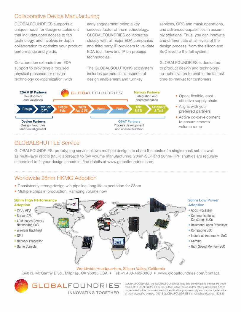
Collaborative Device ManufacturingGLOBALFOUNDRIES supports a unique model for design enablement that includes open access to fab technology, and involves in-depth collaboration to optimize your product performance and yields.
Collaboration extends from EDA support to providing a focused physical presence for design-technology co-optimization, with
early engagement being a key success factor of the methodology. GLOBALFOUNDRIES collaborates closely with all major EDA companies and third party IP providers to validate EDA tool flows and IP on process technologies.
The GLOBALSOLUTIONS ecosystem includes partners in all aspects of design enablement and turnkey
services, OPC and mask operations, and advanced capabilities in assem-bly solutions. Thus, you can innovate and differentiate at all levels of the design process, from the silicon and SoC level to the full system.
GLOBALFOUNDRIES is dedicated to product design and technology co-optimization to enable the fastest time-to-market for customers.
GLOBALSHUTTLE ServiceGLOBALFOUNDRIES’ prototyping service allows multiple designs to share the costs of a single mask set, as well as multi-layer reticle (MLR) approach to low volume manufacturing. 28nm-SLP and 28nm-HPP shuttles are regularly scheduled to fit your design schedule; find details at www.globalfoundries.com.
Worldwide 28nm HKMG Adoption• Consistently strong design win pipeline, long life expectation for 28nm• Multiple chips in production, Ramping volume now
Worldwide Headquarters, Silicon Valley, California 840 N. McCarthy Blvd., Milpitas, CA 95035 USA • Tel: +1 408-462-3900 • www.globalfoundries.com/contact
• Open, flexible, cost- effective supply chain
• Aligns with your preferred partners
• Active co-development to ensure smooth volume ramp
Design PartnersDesign flow, rules and tool alignment
Memory Partners Integration and characterization
EDA & IP Partners Development and validation
OSAT Partners Process development and characterization
Design Test Dev(DFT)
ReticleSets
Wafer Fab & FSI Bump Probe Thin
& BSI Assembly
& Test
28nm Low Power Adoption• Apps Processor
• Communications, Consumer SoCs
• Baseband, Apps Processor
• Computing SoC
• Industrial, Automotive SoC
• Gaming
• High Speed Memory SoC
28nm High Performance Adoption• CPU / APU
• Server CPU
• ARM-based Server / Networking SoC
• Wireless Backhaul
• GPU
• Network Processor
• Game Console