high speed small sectored spi flash memory
TRANSCRIPT
High Speed Small Sectored SPI Flash Memory1M (131,072 x 8)
AT25FS010
5167E–SFLSH–5/09
Features• Serial Peripheral Interface (SPI) Compatible• Supports SPI Modes 0 (0,0) and 3 (1,1)
– Datasheet describes Mode 0 Operation• 50 MHz Clock Rate• Byte Mode and Page Mode Program (1 to 256 Bytes) Operations• Sector/Block/Page Architecture
– 256 byte Pages per Sector– Eight 4 Kbyte Sectors per Block– Four uniform 32 Kbyte Blocks
• Self-timed Sector, Block and Chip Erase• Product Identification Mode with JEDEC Standard• Low-voltage Operation
– 2.7V (VCC = 2.7V to 3.6V)• Hardware and Software Write Protection
– Device protection with Write Protect (WP) Pin– Write Enable and Write Disable Instructions– Software Write Protection:
• Upper 1/32, 1/16, 1/8, 1/4, 1/2 or Entire Array• Flexible Op Codes for Maximum Compatibility• Self-timed Program Cycle
– 30 µs/Byte Typical• Single Cycle Reprogramming (Erase and Program) for Status Register• High Reliability
– Endurance: 10,000 Write Cycles Typical• 8-lead JEDEC 150mil SOIC and 8-lead Ultra Thin Small Array Package (SAP)• Die Sales: Waffer Form, Tape and Reel, and Bumped Waffers
DescriptionThe AT25FS010 provides 1,048,576 bits of serial reprogrammable Flash memoryorganized as 131,072 words of 8 bits each. The device is optimized for use in manyindustrial and commercial applications where low-power and low-voltage operationare essential. The AT25FS010 is available in a space-saving 8-lead JEDEC SOIC and8-lead Ultra Thin SAP packages.Table 0-1. Pin Configuration
Pin Name Function
CS Chip Select
SCK Serial Data Clock
SI Serial Data Input
SO Serial Data Output
GND Ground
VCC Power Supply
WP Write Protect
HOLD Suspends Serial Input
8-lead JEDEC SOIC
1234
8765
CSSOWP
GND
VCCHOLDSCKSI
8-lead SAP
1
2
3
4
8
7
6
5
VCC
HOLD
SCK
SI
CS
SO
WP
GND
___
________
Bottom View
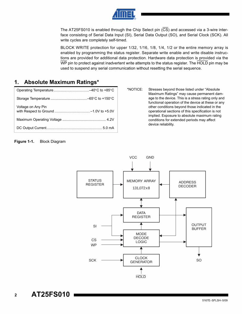
The AT25FS010 is enabled through the Chip Select pin (CS) and accessed via a 3-wire inter-face consisting of Serial Data Input (SI), Serial Data Output (SO), and Serial Clock (SCK). Allwrite cycles are completely self-timed.
BLOCK WRITE protection for upper 1/32, 1/16, 1/8, 1/4, 1/2 or the entire memory array isenabled by programming the status register. Separate write enable and write disable instruc-tions are provided for additional data protection. Hardware data protection is provided via theWP pin to protect against inadvertent write attempts to the status register. The HOLD pin may beused to suspend any serial communication without resetting the serial sequence.
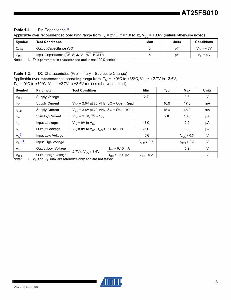
Figure 1-1. Block Diagram
1. Absolute Maximum Ratings*Operating Temperature....................................–40°C to +85°C *NOTICE: Stresses beyond those listed under “Absolute
Maximum Ratings” may cause permanent dam-age to the device. This is a stress rating only and functional operation of the device at these or any other conditions beyond those indicated in the operational sections of this specification is not implied. Exposure to absolute maximum rating conditions for extended periods may affect device reliability.
Storage Temperature .....................................–65°C to +150°C
Voltage on Any Pinwith Respect to Ground ....................................–1.0V to +5.0V
Maximum Operating Voltage ............................................ 4.2V
DC Output Current........................................................ 5.0 mA
131,072 x 8
25167E–SFLSH–5/09
AT25FS010
AT25FS010
Note: 1. This parameter is characterized and is not 100% tested.
Note: 1. VIL and VIH max are reference only and are not tested.
Table 1-1. Pin Capacitance(1)
Applicable over recommended operating range from TA = 25°C, f = 1.0 MHz, VCC = +3.6V (unless otherwise noted)
Symbol Test Conditions Max Units Conditions
COUT Output Capacitance (SO) 8 pF VOUT = 0V
CIN Input Capacitance (CS, SCK, SI, WP, HOLD) 6 pF VIN = 0V
Table 1-2. DC Characteristics (Preliminary – Subject to Change)Applicable over recommended operating range from: TAI = –40°C to +85°C, VCC = +2.7V to +3.6V, TAC = 0°C to +70°C, VCC = +2.7V to +3.6V (unless otherwise noted)
Symbol Parameter Test Condition Min Typ Max Units
VCC Supply Voltage 2.7 3.6 V
ICC1 Supply Current VCC = 3.6V at 20 MHz, SO = Open Read 10.0 17.0 mA
ICC2 Supply Current VCC = 3.6V at 20 MHz, SO = Open Write 15.0 45.0 mA
ISB Standby Current VCC = 2.7V, CS = VCC 2.0 10.0 µA
IIL Input Leakage VIN = 0V to VCC -3.0 3.0 µA
IOL Output Leakage VIN = 0V to VCC, TAC = 0°C to 70°C -3.0 3.0 µA
VIL(1) Input Low Voltage -0.6 VCC x 0.3 V
VIH(1) Input High Voltage VCC x 0.7 VCC + 0.5 V
VOL Output Low Voltage2.7V ≤ VCC ≤ 3.6V
IOL = 0.15 mA 0.2 V
VOH Output High Voltage IOH = -100 µA VCC - 0.2 V
35167E–SFLSH–5/09
Notes: 1. The programming time for n bytes will be equal to n x tBPC.2. This parameter is ensured by characterization at 3.0v, 25c only.3. One write cycle consists of erasing a sector, followed by programming the same sector.
Table 1-3. AC Characteristics (Preliminary – Subject to Change)Applicable over recommended operating range from TA = –40°C to +85°C, VCC = +2.7V to +3.6VCL = 1 TTL Gate and 30 pF (unless otherwise noted)
Symbol Parameter Min Typ Max Units
fSCK SCK Clock Frequency 0 50 MHz
tRI Input Rise Time 5 ns
tFI Input Fall Time 5 ns
tWH SCK High Time 9 ns
tWL SCK Low Time 9 ns
tCS CS High Time 100 ns
tCSS CS Setup Time 5 ns
tCSH CS Hold Time 5 ns
tSU Data In Setup Time 5 ns
tH Data In Hold Time 5 ns
tHD Hold Setup Time 5 ns
tCD Hold Hold Time 5 ns
tV Output Valid 9 ns
tHO Output Hold Time 0 ns
tLZ Hold to Output Low Z 9 ns
tHZ Hold to Output High Z 9 ns
tDIS Output Disable Time 9 ns
tse Sector Erase Time 50 200 ms
tbe Block Erase Time 200 500 ms
tce Chip Erase Time 1.6 4 s
tSR Status Register Write Cycle Time 60 ms
tBPC Byte Program Cycle Time(1) 30 50 µs
Endurance(2) 10K Write Cycles(3)
45167E–SFLSH–5/09
AT25FS010
AT25FS010
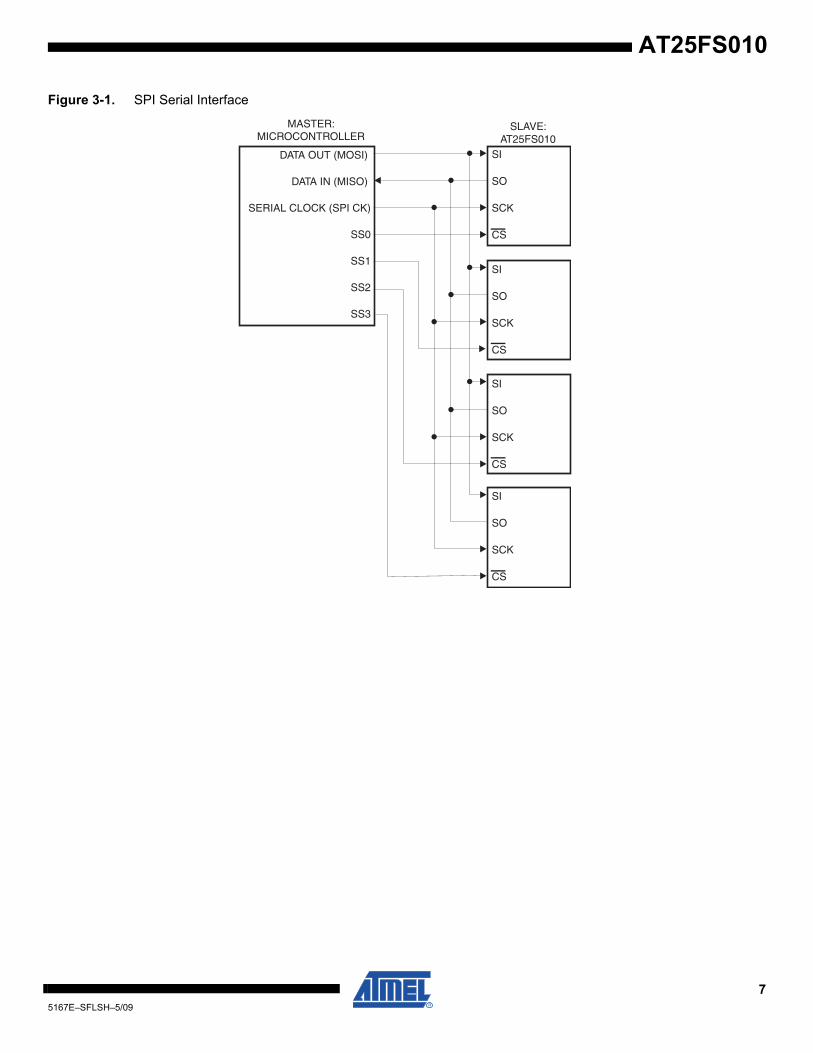
2. Serial Interface DescriptionMASTER: The device that generates the serial clock.
SLAVE: Because the Serial Clock pin (SCK) is always an input, the AT25FS010 always oper-ates as a slave.
TRANSMITTER/RECEIVER: The AT25FS010 has separate pins designated for data transmis-sion (SO) and reception (SI).
MSB: The Most Significant Bit (MSB) is the first bit transmitted and received.
SERIAL OP-CODE: After the device is selected with CS going low, the first byte will bereceived. This byte contains the op-code that defines the operations to be performed.
INVALID OP-CODE: If an invalid op-code is received, no data will be shifted into theAT25FS010, and the serial output pin (SO) will remain in a high impedance state until the fallingedge of CS is detected again. This will reinitialize the serial communication.
CHIP SELECT: The AT25FS010 is selected when the CS pin is low. When the device is notselected, data will not be accepted via the SI pin, and the serial output pin (SO) will remain in ahigh impedance state.
HOLD: The HOLD pin is used in conjunction with the CS pin to select the AT25FS010. Whenthe device is selected and a serial sequence is underway, HOLD can be used to pause the serialcommunication with the master device without resetting the serial sequence. To pause, theHOLD pin must be brought low while the SCK pin is low. To resume serial communication, theHOLD pin is brought high while the SCK pin is low (SCK may still toggle during HOLD). Inputs tothe SI pin will be ignored while the SO pin is in the high impedance state.
WRITE PROTECT: The AT25FS010 has a write lockout feature that can be activated by assert-ing the write protect pin (WP). When the lockout feature is activated, locked-out sectors will beREAD only. The write protect pin will allow normal read/write operations when held high. Whenthe WP is brought low and WPEN bit is “1”, all write operations to the status register are inhib-ited. WP going low while CS is still low will interrupt a write to the status register. If the internalstatus register write cycle has already been initiated, WP going low will have no effect on anywrite operation to the status register. The WP pin function is blocked when the WPEN bit in thestatus register is “0”. This will allow the user to install the AT25FS010 in a system with the WPpin tied to ground and still be able to write to the status register. All WP pin functions are enabledwhen the WPEN bit is set to “1”.
55167E–SFLSH–5/09
3. Operating Features
3.1 Recommended Power-upWhen the power supply is turned on, Vcc rises monotonically from ground to the full operatingVcc. During this time, the Chip Select (CS) signal is not allowed to float and must follow Vcc. Forthis reason, it is recommended to use a suitable pull-up resistor connected between CS and Vcc.The device is ready for communication once a stable Vcc is reached within the specified operat-ing voltage range.
3.2 Recommended Power-downThe device must be deselected and in Standby and Write Disabled mode prior to Vcc powerdown sequence. This means there should be no write operation/internal Write cycle or readoperation in progress during the Chip Select (CS) line must be allowed to follow Vcc during powerdown. After power down, it is recommended Vcc should be held at ground level for at least 0.5seconds before power up again.
3.3 Power On Reset ProtectionIn order to prevent data corruption and inadvertent Write operations during device power-up andpower down, a Power On Reset (POR) circuit is enabled. At Power-up (continuous rise of Vccfrom 0v), the device will not respond to any instruction and will be held in reset (which puts thedevice in standby mode) until the Vcc has reached the Power On Reset threshold voltage. Thisthreshold is lower than the minimum specified Vcc operation voltage.
At power down (continuous fall of Vcc), when Vcc drops from the operating voltage below thePOR threshold, all operations are disabled and the device will not respond to any command. Astable and valid Vcc must be applied before executing and communication.
Please note: The POR threshold trip point is ~1.8v for Serial Flash products and is ensured bydesign to have a reset during power up and power down and is not 100% tested.
65167E–SFLSH–5/09
AT25FS010
AT25FS010
Figure 3-1. SPI Serial Interface
MASTER:MICROCONTROLLER
SLAVE:AT25FS010
DATA OUT (MOSI)
DATA IN (MISO)
SERIAL CLOCK (SPI CK)
SS0
SS1
SS2
SS3
SI
SO
SCK
CS
SI
SO
SCK
CS
SI
SO
SCK
CS
SI
SO
SCK
CS
75167E–SFLSH–5/09
4. Functional DescriptionThe AT25FS010 is designed to interface directly with the synchronous serial peripheral interface(SPI) of the 6800 type series of microcontrollers.
The AT25FS010 utilizes an 8-bit instruction register. The list of instructions and their operationcodes are contained in Table 4-1. All instructions, addresses, and data are transferred with theMSB first and start with a high-to-low transition.
Write is defined as program and/or erase in this specification. The following commands, PRO-GRAM, SECTOR ERASE, BLOCK ERASE, CHIP ERASE, and WRSR are write instructions forAT25FS010.
Note: 1. Either one of the OP CODES will execute the instruction.
WRITE ENABLE (WREN): The device will power up in the write disable state when VCC isapplied. All write instructions must therefore be preceded by the WREN instruction.
WRITE DISABLE (WRDI): To protect the device against inadvertent writes, the WRDI instruc-tion disables all write commands. The WRDI instruction is independent of the status of the WPpin.
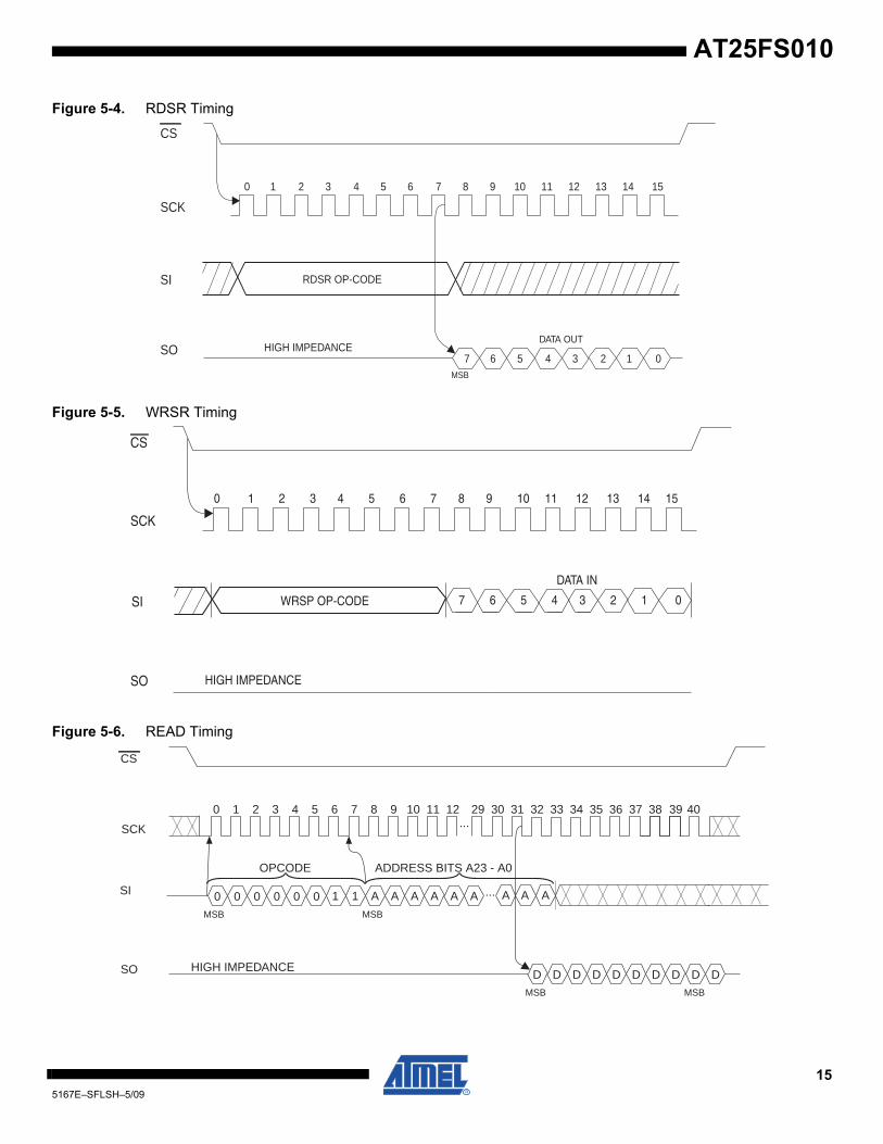
READ STATUS REGISTER (RDSR): The RDSR instruction provides access to the status regis-ter. The READY/BUSY and write enable status of the device can be determined by the RDSRinstruction. Similarly, the Block Write Protection bits indicate the extent of protection employed.
Table 4-1. Instruction Set for the AT25FS010
Instruction Name One Byte OpCode Operation
Binary Hex
WREN 0000 X110 06 Set Write Enable Latch
WRDI 0000 X100 04 Reset Write Enable Latch
RDSR 0000 X101 05 Read Status Register
WRSR 0000 X001 01 Write Status Register
READ 0000 0011 03 Read Data from Memory Array
FAST READ 0000 1011 0B Read Data from Memory Array (with dummy cycles)
PROGRAM 0000 X010 02 Program Data Into Memory Array
SECTOR ERASE (1)
0010 0000 20 Erase One 4kbyte Sector in Memory Array
1101 0111 D7
BLOCK ERASE(1)0101 0010 52 Erase One 32kbyte Block in Memory Array
1101 1000 D8
CHIP ERASE(1)0110 0000 60 Erase All Memory Array
1100 0111 C7
RDID(1)1001 1111 9F Read Manufacturer and Product ID
1010 1011 AB
85167E–SFLSH–5/09
AT25FS010
AT25FS010
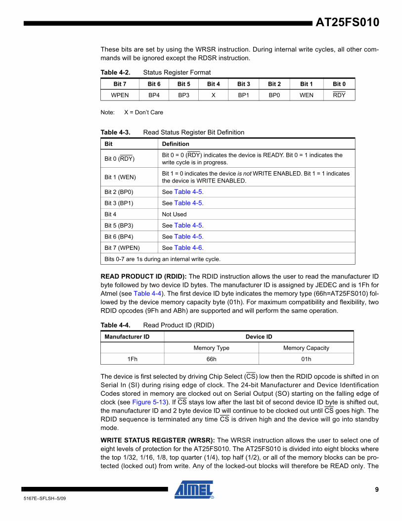
These bits are set by using the WRSR instruction. During internal write cycles, all other com-mands will be ignored except the RDSR instruction.
Note: X = Don’t Care
READ PRODUCT ID (RDID): The RDID instruction allows the user to read the manufacturer IDbyte followed by two device ID bytes. The manufacturer ID is assigned by JEDEC and is 1Fh forAtmel (see Table 4-4). The first device ID byte indicates the memory type (66h=AT25FS010) fol-lowed by the device memory capacity byte (01h). For maximum compatibility and flexibility, twoRDID opcodes (9Fh and ABh) are supported and will perform the same operation.
The device is first selected by driving Chip Select (CS) low then the RDID opcode is shifted in onSerial In (SI) during rising edge of clock. The 24-bit Manufacturer and Device IdentificationCodes stored in memory are clocked out on Serial Output (SO) starting on the falling edge ofclock (see Figure 5-13). If CS stays low after the last bit of second device ID byte is shifted out,the manufacturer ID and 2 byte device ID will continue to be clocked out until CS goes high. TheRDID sequence is terminated any time CS is driven high and the device will go into standbymode.
WRITE STATUS REGISTER (WRSR): The WRSR instruction allows the user to select one ofeight levels of protection for the AT25FS010. The AT25FS010 is divided into eight blocks wherethe top 1/32, 1/16, 1/8, top quarter (1/4), top half (1/2), or all of the memory blocks can be pro-tected (locked out) from write. Any of the locked-out blocks will therefore be READ only. The
Table 4-2. Status Register Format
Bit 7 Bit 6 Bit 5 Bit 4 Bit 3 Bit 2 Bit 1 Bit 0
WPEN BP4 BP3 X BP1 BP0 WEN RDY
Table 4-3. Read Status Register Bit Definition
Bit Definition
Bit 0 (RDY) Bit 0 = 0 (RDY) indicates the device is READY. Bit 0 = 1 indicates the write cycle is in progress.
Bit 1 (WEN) Bit 1 = 0 indicates the device is not WRITE ENABLED. Bit 1 = 1 indicates the device is WRITE ENABLED.
Bit 2 (BP0) See Table 4-5.
Bit 3 (BP1) See Table 4-5.
Bit 4 Not Used
Bit 5 (BP3) See Table 4-5.
Bit 6 (BP4) See Table 4-5.
Bit 7 (WPEN) See Table 4-6.
Bits 0-7 are 1s during an internal write cycle.
Table 4-4. Read Product ID (RDID)
Manufacturer ID Device ID
Memory Type Memory Capacity
1Fh 66h 01h
95167E–SFLSH–5/09
locked-out sector/block and the corresponding status register control bits are shown in Table 4-5on page 10.
The six bits, BP0, BP1, BP3, BP4 and WPEN, are nonvolatile cells that have the same proper-ties and functions as the regular memory cells.
Note: 1. x = don’t careThe WRSR instruction also allows the user to enable or disable the Write Protect (WP) pinthrough the use of the Write Protect Enable (WPEN) bit. Hardware write protection is enabledwhen the WP pin is low and the WPEN bit is “1”. Hardware write protection is disabled wheneither the WP pin is high or the WPEN bit is “0.” When the device is hardware write protected,writes to the Status Register, including the Block Protect bits and the WPEN bit, and the locked-out sectors in the memory array are disabled. Write is only allowed to sectors of the memorywhich are not locked out. The WRSR instruction is self-timed to automatically erase and pro-gram BP0, BP1, BP3, BP4 and WPEN bits. In order to write the status register, two separateinstructions must be executed. First, the device must be write enabled via the WREN instruction.Then, CS must be low and the WRSR instruction and data for the six bits are entered. TheWRSR write cycle will begin once CS goes high. During the internal write cycle, all instructionswill be ignored except RDSR instructions. The AT25FS010 will automatically return to write dis-able state at the completion of the WRSR cycle. The status register is factory programmed to all0’s.
Note: When the WPEN bit is hardware write protected, it cannot be changed back to “0”, as long as the WP pin is held low.
Table 4-5. Sector/Block Write Protect Bits
Level Status Register Bits AT25FS010
BP4 BP3 BP1 BP0 Array Address
locked Out Locked-out Blocks
0(none) 0 0 0 0 None None
1(1/32) 0 1 0 0 01F000H − 01FFFFH Sector 8 of Block 4
2(1/16) 1 0 0 0 01E000H − 01FFFFH Sector 7 − 8 of Block 4
3(1/8) 1 1 0 0 01C000H − 01FFFFH Sector 5 − 8 of Block 4
4(1/4) x x 0 1 018000H − 01FFFFH ALL Sectors of Block 4
5(1/2) x x 1 0 010000H − 01FFFFH ALL Sectors of Block 3,4
6(ALL) x x 1 1 000000H − 01FFFFH ALL Sectors of ALL Blocks (1-4)
Table 4-6. WPEN Operation
WPEN WP WEN ProtectedBlocks UnprotectedBlocks Status Register
0 X 0 Protected Protected Protected
0 X 1 Protected Writable Writable
1 Low 0 Protected Protected Protected
1 Low 1 Protected Writable Protected
X High 0 Protected Protected Protected
X High 1 Protected Writable Writable
105167E–SFLSH–5/09
AT25FS010
AT25FS010
READ (READ): The READ instruction sequence reads the memory array up to the maximumspeed of 50MHz. Reading the AT25FS010 via the SO (Serial Output) pin requires the followingsequence. After the CS line is pulled low to select the device, the READ instruction is clocked inon the SI line, followed by the byte address to be read. Upon completion, any data on the SI linewill be ignored. The data (D7-D0) at the specified address is then shifted out onto the SO line(see Figure 5-6). If only one byte is to be read, the CS line should be driven high after the leastsignificant data bit. To continue read operation and sequentially read subsequent byteaddresses from the device by simply keeping CS low and provide a clock signal. The deviceincorporates an internal address counter that automatically increments to the next byte addressduring sequential read operation. The READ instruction can be continued since the byteaddress is automatically incremented and data will continue to be shifted out of the AT25FS010until the highest byte address is reached. When the last bit of the memory has been read, thedevice will continue reading back at the beginning of the array (000000h) without delay. Thedata is always output from the device with the most significant bit (MSB) of a byte first. TheREAD sequence is terminated any time CS is driven high and the device will go into standbymode.
FAST READ (FAST READ): The FAST READ instruction sequence reads the memory array upto the maximum speed of 50MHz (same as standard READ sequence). The FAST READ is analternate command for the READ and allows for FAST READ instruction compatibility support.The difference between the two is FAST READ requires a “dummy byte” and READ does not.Reading the AT25FS010 via the SO (Serial Output) pin requires the following sequence. Afterthe CS line is pulled low to select the device, the FAST READ instruction is clocked in on the SIline, followed by the byte address to be read and the dummy byte (the SO line output will be highZ state). Upon completion, any data on the SI line will be ignored. The data (D7-D0) at the spec-ified address is then shifted out onto the SO line (see Figure 5-7). If only one byte is to be read,the CS line should be driven high after the least significant data bit. To continue read operationand sequentially read subsequent byte addresses from the device by simply keeping CS lowand provide a clock signal. The device incorporates an internal address counter that automati-cally increments to the next byte address during sequential read operation. The FAST READinstruction can be continued since the byte address is automatically incremented and data willcontinue to be shifted out of the AT25FS010 until the highest address is reached. When the lastbit of the memory has been read, the device will continue reading back at the beginning of thearray (000000h) without delay. The data is always output from the device with the most signifi-cant bit (MSB) of a byte first. The FAST READ sequence is terminated any time CS is drivenhigh and the device will go into standby mode.
PROGRAM (PROGRAM): The PROGRAM instruction allows up to 256 data bytes to be writtento each page in the memory in one-operation changing data bits from a logic 1 to 0 state. TheAT25FS010 memory array contains 131,072 programmable data bytes internally organized into256 bytes per page with a total of 512 pages in the memory.
In order to program the AT25FS010, two separate instructions must be executed. First, thedevice must be write enabled via the WREN instruction. Then the PROGRAM instruction can beexecuted and requires the following sequence. After the CS line is pulled low to select thedevice, the PROGRAM instruction is clocked in via the SI line followed by the byte address (seeFigure 5-8) and the data byte(s) to be programmed. Programming will start after CS pin isbrought high. Please note: The low to high transition of the CS pin must occur during the SCKlow time immediately after clocking in the D0 (LSB) data bit to initiate programming cycle. Also, aWREN instruction must precede each and every PROGRAM instruction. The Ready/Busy statusof the device can be determined by initiating a RDSR instruction. If bit 0=1, the program cycle is
115167E–SFLSH–5/09
still in progress. If Bit 0=0, the programming cycle has ended. Only the RDSR instruction isenabled during the programming cycle and all other opcode instructions are ignored until pro-gramming cycle has completed.
A single PROGRAM instruction programs 1 to 256 consecutive bytes within a page if it is notwrite protected. The starting byte address can be anywhere within the page. When the end ofthe page is reached, the address will wrap around to the beginning of the same page. If the datato be programmed is less than a full page, the data of all other bytes on the same page willremain unchanged meaning that the unwritten address locations within the page will not bechanged. If more than 256 bytes of data are provided, the address counter will roll over on thesame page and the previous data provided will be replaced. The same byte cannot be repro-grammed without erasing the whole sector or block first. The AT25FS010 will automaticallyreturn to the write disable state at the completion of the programming cycle.
Note: If the device is not write enabled (WREN), the device will ignore the Write instruction and will return to the standby state when CS is brought high. A new CS falling edge is required to re-initi-ate the serial communication.
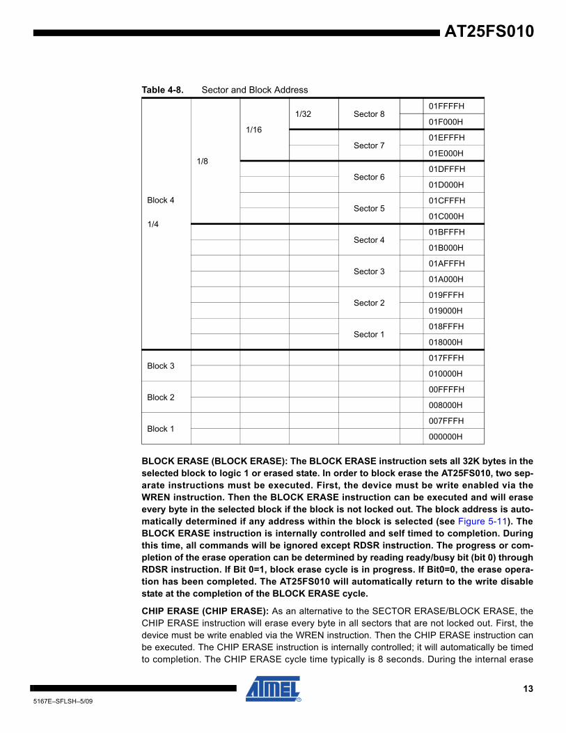
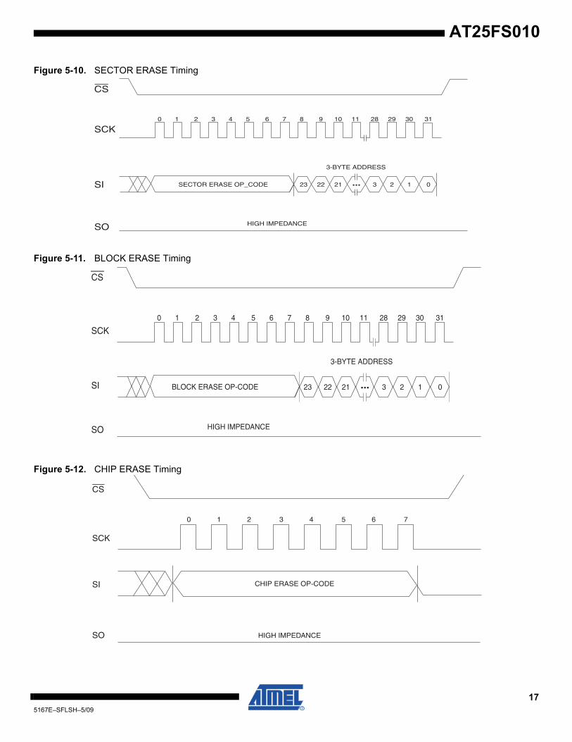
ERASE OPERATION: The AT25FS010 memory array is internally organized into uniform4K byte sectors or uniform 32K byte uniform blocks (see Table 4-8). Before data can bereprogrammed, the sector or block that contains the data must be erased first. In order toerase the AT25FS010, there are three flexible erase instructions that can be executed asfollows: SECTOR ERASE, BLOCK ERASE and CHIP ERASE instructions. A SECTORERASE instruction allows erasing any individual 4K sector without changing data in restof memory. The BLOCK ERASE instruction allows erasing any individual block and CHIPERASE allows erasing the entire memory array.
SECTOR ERASE (SECTOR ERASE): The SECTOR ERASE instruction sets all 4K bytes in theselected sector to logic 1 or erased state. In order to sector erase the AT25FS010, two separateinstructions must be executed. First, the device must be write enabled via the WREN instruction.Then the SECTOR ERASE instruction can be executed and will erase every byte in the selectedsector if the sector is not locked out. The sector address is automatically determined if anyaddress within the sector is selected (see Figure 5-10). The SECTOR ERASE instruction isinternally controlled and self timed to completion. During this time, all commands will be ignoredexcept RDSR instruction. The progress or completion of the erase operation can be determinedby reading ready/busy bit (bit 0) through RDSR instruction. If Bit 0=1, sector erase cycle is inprogress. If Bit 0=0, the erase operation has been completed. The AT25FS010 will automaticallyreturn to the write disable state at the completion of the SECTOR ERASE cycle.
Table 4-7. Address Key
Address AT25FS010
AN A15 - A0
Don’t Care Bits A23 - A17
125167E–SFLSH–5/09
AT25FS010
AT25FS010
BLOCK ERASE (BLOCK ERASE): The BLOCK ERASE instruction sets all 32K bytes in theselected block to logic 1 or erased state. In order to block erase the AT25FS010, two sep-arate instructions must be executed. First, the device must be write enabled via theWREN instruction. Then the BLOCK ERASE instruction can be executed and will eraseevery byte in the selected block if the block is not locked out. The block address is auto-matically determined if any address within the block is selected (see Figure 5-11). TheBLOCK ERASE instruction is internally controlled and self timed to completion. Duringthis time, all commands will be ignored except RDSR instruction. The progress or com-pletion of the erase operation can be determined by reading ready/busy bit (bit 0) throughRDSR instruction. If Bit 0=1, block erase cycle is in progress. If Bit0=0, the erase opera-tion has been completed. The AT25FS010 will automatically return to the write disablestate at the completion of the BLOCK ERASE cycle.
CHIP ERASE (CHIP ERASE): As an alternative to the SECTOR ERASE/BLOCK ERASE, theCHIP ERASE instruction will erase every byte in all sectors that are not locked out. First, thedevice must be write enabled via the WREN instruction. Then the CHIP ERASE instruction canbe executed. The CHIP ERASE instruction is internally controlled; it will automatically be timedto completion. The CHIP ERASE cycle time typically is 8 seconds. During the internal erase
Table 4-8. Sector and Block Address
Block 4
1/4
1/8
1/16
1/32 Sector 801FFFFH
01F000H
Sector 701EFFFH
01E000H
Sector 601DFFFH
01D000H
Sector 501CFFFH
01C000H
Sector 401BFFFH
01B000H
Sector 301AFFFH
01A000H
Sector 2019FFFH
019000H
Sector 1 018FFFH
018000H
Block 3017FFFH
010000H
Block 200FFFFH
008000H
Block 1007FFFH
000000H
135167E–SFLSH–5/09
cycle, all instructions will be ignored except RDSR. The AT25FS010 will automatically return tothe write disable state at the completion of the CHIP ERASE cycle.
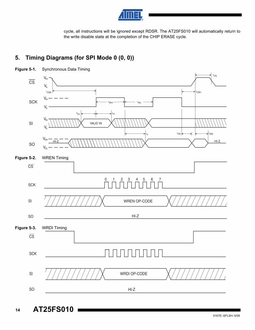
5. Timing Diagrams (for SPI Mode 0 (0, 0))
Figure 5-1. Synchronous Data Timing
Figure 5-2. WREN Timing
Figure 5-3. WRDI Timing
VOH
VOL
HI-Z HI-Z
tV
VALID INVIH
VIL
tHtSU
tDIS
VIH
VIL
tWH
tCSH
VIH
VIL
tCSS
tCS
tWL
tHO
CS
SCK
SI
SO
0 1 2 3 4 5 6 7
HI-Z
WREN OP-CODE
CS
SCK
SI
SO
HI-Z
WRDI OP-CODE
CS
SCK
SI
SO
145167E–SFLSH–5/09
AT25FS010
AT25FS010
Figure 5-4. RDSR Timing
Figure 5-5. WRSR Timing
Figure 5-6. READ Timing
CS
SCK
0 1 2 3 4 5 6 7 8 9 10 11 12 13 14 15
SI
SO7 6 5 4 3 2 1 0
DATA OUT
MSB
HIGH IMPEDANCE
RDSR OP-CODE
HIGH IMPEDANCE
WRSP OP-CODE
DATA IN
7 6 5 4 3 2 1 0
0 1 2 3 4 5 6 7 8 9 10 11 12 13 14 15
CS
SCK
SI
SO
CS
SI
SCK
HIGH IMPEDANCE
ADDRESS BITS A23 - A0
0 1 2 3 4
D
5
D
6
D
7
D
8 9 10 11 12
... A A
D D
A
29 30 31 32 33 34 35 36 37 38 39 40
SO
...
AA11 A A A A00 0 0 0 0MSB MSB
MSB MSB
OPCODE
D DD D
155167E–SFLSH–5/09
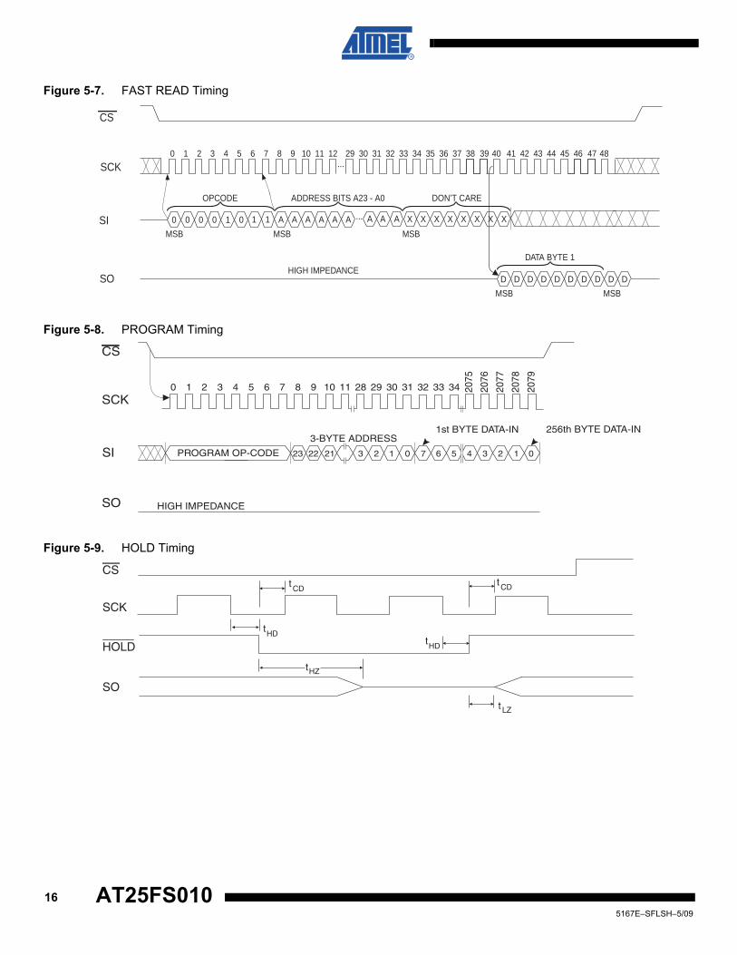
Figure 5-7. FAST READ Timing
Figure 5-8. PROGRAM Timing
Figure 5-9. HOLD Timing
CS
SI
SCK
HIGH IMPEDANCE
ADDRESS BITS A23 - A0 DON’T CARE
0 1 2 3 4
D
5
D
6
D
7
D
8 9 10 11 12
... A A
D D
A
29 30 31 32 33 34 35 36 37 38 39 40
SO
41 42 43 44 45 46 47 48...
AA11 A A A A00 0 0 1 0 XXXX X X X X
MSB MSB MSB
MSB MSB
OPCODE
D DD D
DATA BYTE 1
CS
SCK
SI
SO
3-BYTE ADDRESS1st BYTE DATA-IN 256th BYTE DATA-IN
HIGH IMPEDANCE
0 1 2 3 4 5 6 7 8 9 10 11 28
23 22 21 3 1 0 6 5 4 3 2 1 072
29 30 31 32 33 34 2075
2076
2078
2077
2079
PROGRAM OP-CODE
CS
SCK
HOLD
SO
tCD
tHD
tHZ
t LZ
tHD
tCD
165167E–SFLSH–5/09
AT25FS010
AT25FS010
Figure 5-10. SECTOR ERASE Timing
Figure 5-11. BLOCK ERASE Timing
Figure 5-12. CHIP ERASE Timing
CS
SCK
SI
SO
0 1 2 3 4 5 6 7 8 9 10 11 28 29 30 31
3-BYTE ADDRESS
HIGH IMPEDANCE
23 22 21 3 2 1 0SECTOR ERASE OP_CODE
BLOCK ERASE OP-CODE
CS
SCK
SI
SO
0 1 2 3 4 5 6 7 8 9 10 11 28 29 30 31
3-BYTE ADDRESS
HIGH IMPEDANCE
23 22 21 3 2 1 0
CS
SCK
SI
SO HIGH IMPEDANCE
CHIP ERASE OP-CODE
0 1 2 3 4 5 6 7
175167E–SFLSH–5/09
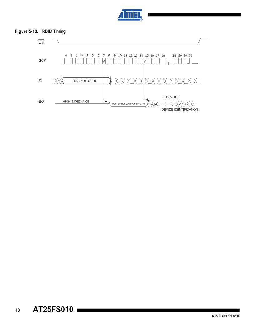
Figure 5-13. RDID Timing
12 13 14 15 16 17 18 31
CS
SCK
SI
SO
0 1 2 3 4 5 6 7 8 9 10 11
HIGH IMPEDANCE
28 29 30
DATA OUT
15 14 3 2 1 0
DEVICE IDENTIFICATION
Manufacturer Code (Atmel = 1Fh)
RDID OP-CODE
185167E–SFLSH–5/09
AT25FS010
AT25FS010
Notes: 1. “-B” designates bulk ordering code.2. “-T” designates tape and reel ordering code. SOIC=4K per reel and SAP=3K per reel.
Ordering InformationOrdering Code Package Operation RangeAT25FS010N-SH27-B(1) 8S1 Lead-Free/Halogen-Free/
NiPdAu Lead FinishIndustrial Temperature
(–40°C to 85°C)
AT25FS010N-SH27-T(2) 8S1
AT25FS010Y7-YH27-T(2)8Y7
Package Type
8S1 8-lead, 0.150” Wide, Plastic Gull Wing Small outline (JEDEC SOIC)
8Y7 8-lead, 6.00 mm x 4.90 mm Body, Ultra Thin, Dual Footprint, Non-leaded, Small Array Package (SAP)
Options
–2.7 Low Voltage (2.7V to 3.6V)
195167E–SFLSH–5/09
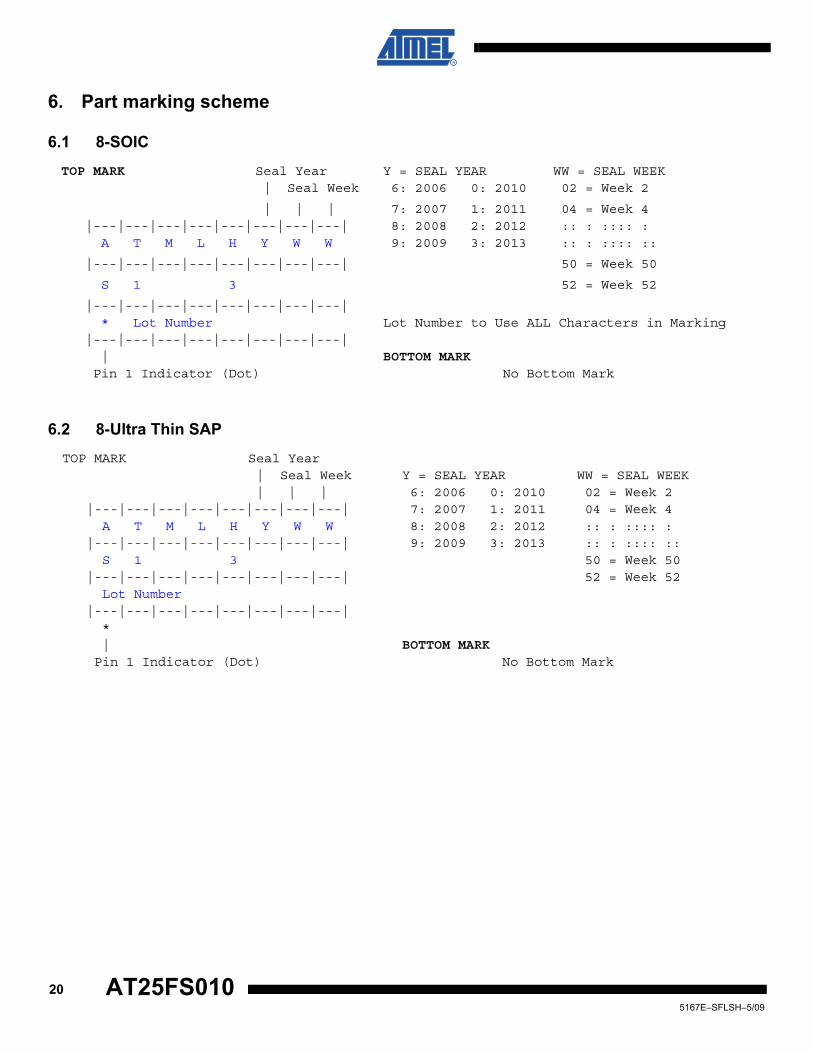
6. Part marking scheme
6.1 8-SOIC
6.2 8-Ultra Thin SAP
TOP MARK Seal Year Y = SEAL YEAR WW = SEAL WEEK | Seal Week 6: 2006 0: 2010 02 = Week 2
| | | 7: 2007 1: 2011 04 = Week 4 |---|---|---|---|---|---|---|---| 8: 2008 2: 2012 :: : :::: : A T M L H Y W W 9: 2009 3: 2013 :: : :::: ::
|---|---|---|---|---|---|---|---| 50 = Week 50
S 1 3 52 = Week 52
|---|---|---|---|---|---|---|---| * Lot Number Lot Number to Use ALL Characters in Marking |---|---|---|---|---|---|---|---| | BOTTOM MARK Pin 1 Indicator (Dot) No Bottom Mark
TOP MARK Seal Year | Seal Week Y = SEAL YEAR WW = SEAL WEEK | | | 6: 2006 0: 2010 02 = Week 2
|---|---|---|---|---|---|---|---| 7: 2007 1: 2011 04 = Week 4 A T M L H Y W W 8: 2008 2: 2012 :: : :::: : |---|---|---|---|---|---|---|---| 9: 2009 3: 2013 :: : :::: :: S 1 3 50 = Week 50 |---|---|---|---|---|---|---|---| 52 = Week 52 Lot Number |---|---|---|---|---|---|---|---| * | BOTTOM MARK Pin 1 Indicator (Dot) No Bottom Mark
205167E–SFLSH–5/09
AT25FS010
AT25FS010
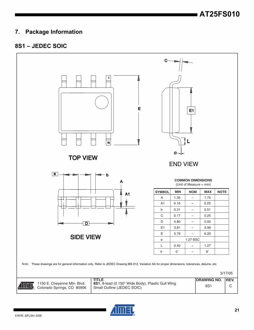
7. Package Information
8S1 – JEDEC SOIC
1150 E. Cheyenne Mtn. Blvd.Colorado Springs, CO 80906
TITLE DRAWING NO.
R
REV.
Note:
3/17/05
8S1, 8-lead (0.150" Wide Body), Plastic Gull Wing Small Outline (JEDEC SOIC) 8S1 C
COMMON DIMENSIONS(Unit of Measure = mm)
SYMBOL MIN NOM MAX NOTE
A1 0.10 – 0.25
These drawings are for general information only. Refer to JEDEC Drawing MS-012, Variation AA for proper dimensions, tolerances, datums, etc.
A 1.35 – 1.75
b 0.31 – 0.51
C 0.17 – 0.25
D 4.80 – 5.05
E1 3.81 – 3.99
E 5.79 – 6.20
e 1.27 BSC
L 0.40 – 1.27
θ 0˚ – 8˚
ØØ
EE
11
NN
TOP VIEWTOP VIEW
CC
E1E1
END VIEW
AA
bb
LL
A1A1
ee
DD
SIDE VIEWSIDE VIEW
215167E–SFLSH–5/09
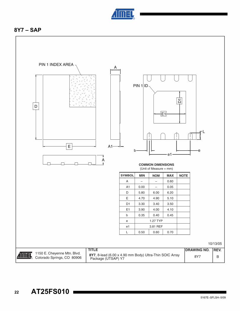
8Y7 – SAP
1150 E. Cheyenne Mtn. Blvd.Colorado Springs, CO 80906
TITLE DRAWING NO.
R
REV. 8Y7, 8-lead (6.00 x 4.90 mm Body) Ultra-Thin SOIC Array Package (UTSAP) Y7 B8Y7
10/13/05
COMMON DIMENSIONS(Unit of Measure = mm)
SYMBOL MIN NOM MAX NOTE
A – – 0.60
A1 0.00 – 0.05
D 5.80 6.00 6.20
E 4.70 4.90 5.10
D1 3.30 3.40 3.50
E1 3.90 4.00 4.10
b 0.35 0.40 0.45
e 1.27 TYP
e1 3.81 REF
L 0.50 0.60 0.70
D1
PIN 1 ID
E1
L
be1
e
PIN 1 INDEX AREA
A
E
D
A1
A
225167E–SFLSH–5/09
AT25FS010
AT25FS010
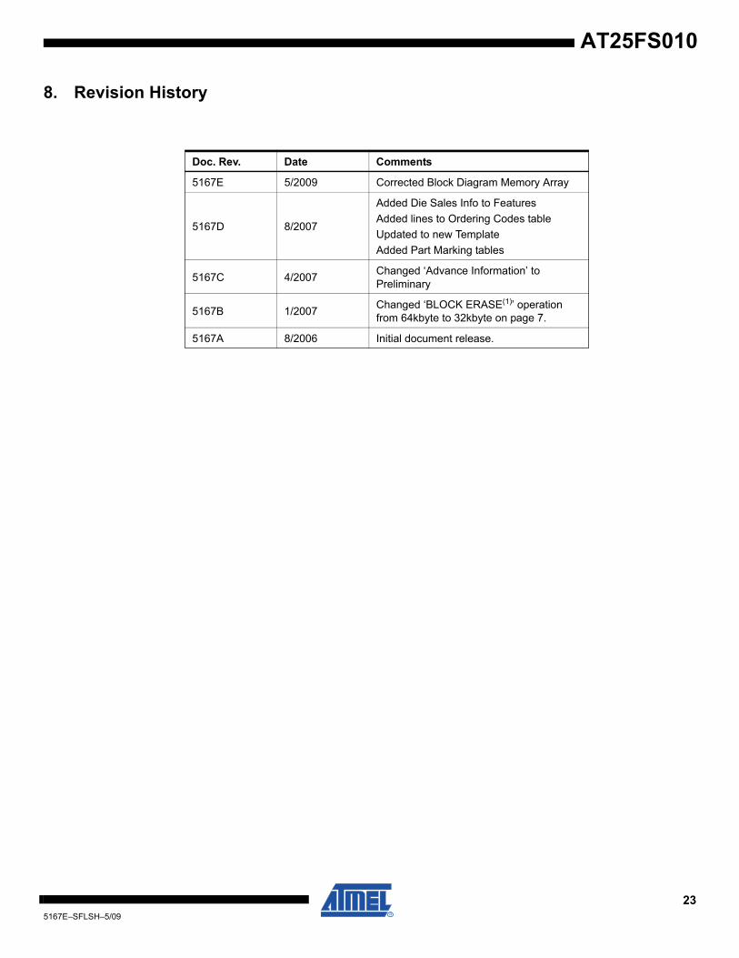
8. Revision History
Doc. Rev. Date Comments
5167E 5/2009 Corrected Block Diagram Memory Array
5167D 8/2007
Added Die Sales Info to FeaturesAdded lines to Ordering Codes tableUpdated to new TemplateAdded Part Marking tables
5167C 4/2007 Changed ‘Advance Information’ to Preliminary
5167B 1/2007 Changed ‘BLOCK ERASE(1)’ operation from 64kbyte to 32kbyte on page 7.
5167A 8/2006 Initial document release.
235167E–SFLSH–5/09
5167E–SFLSH–5/09
Headquarters International
Atmel Corporation2325 Orchard ParkwaySan Jose, CA 95131USATel: 1(408) 441-0311Fax: 1(408) 487-2600
Atmel AsiaRoom 1219Chinachem Golden Plaza77 Mody Road TsimshatsuiEast KowloonHong KongTel: (852) 2721-9778Fax: (852) 2722-1369
Atmel EuropeLe Krebs8, Rue Jean-Pierre TimbaudBP 30978054 Saint-Quentin-en-Yvelines CedexFranceTel: (33) 1-30-60-70-00 Fax: (33) 1-30-60-71-11
Atmel Japan9F, Tonetsu Shinkawa Bldg.1-24-8 ShinkawaChuo-ku, Tokyo 104-0033JapanTel: (81) 3-3523-3551Fax: (81) 3-3523-7581
Product Contact
Web Sitewww.atmel.com
Technical [email protected]
Sales Contactwww.atmel.com/contacts
Literature Requestswww.atmel.com/literature
Disclaimer: The information in this document is provided in connection with Atmel products. No license, express or implied, by estoppel or otherwise, to anyintellectual property right is granted by this document or in connection with the sale of Atmel products. EXCEPT AS SET FORTH IN ATMEL’S TERMS AND CONDI-TIONS OF SALE LOCATED ON ATMEL’S WEB SITE, ATMEL ASSUMES NO LIABILITY WHATSOEVER AND DISCLAIMS ANY EXPRESS, IMPLIED OR STATUTORYWARRANTY RELATING TO ITS PRODUCTS INCLUDING, BUT NOT LIMITED TO, THE IMPLIED WARRANTY OF MERCHANTABILITY, FITNESS FOR A PARTICULARPURPOSE, OR NON-INFRINGEMENT. IN NO EVENT SHALL ATMEL BE LIABLE FOR ANY DIRECT, INDIRECT, CONSEQUENTIAL, PUNITIVE, SPECIAL OR INCIDEN-TAL DAMAGES (INCLUDING, WITHOUT LIMITATION, DAMAGES FOR LOSS OF PROFITS, BUSINESS INTERRUPTION, OR LOSS OF INFORMATION) ARISING OUTOF THE USE OR INABILITY TO USE THIS DOCUMENT, EVEN IF ATMEL HAS BEEN ADVISED OF THE POSSIBILITY OF SUCH DAMAGES. Atmel makes norepresentations or warranties with respect to the accuracy or completeness of the contents of this document and reserves the right to make changes to specificationsand product descriptions at any time without notice. Atmel does not make any commitment to update the information contained herein. Unless specifically providedotherwise, Atmel products are not suitable for, and shall not be used in, automotive applications. Atmel’s products are not intended, authorized, or warranted for useas components in applications intended to support or sustain life.
© 2009 Atmel Corporation. All rights reserved. Atmel®, Atmel logo and combinations thereof and others, are registered trademarks or trade-marks of Atmel Corporation or its subsidiaries. Other terms and product names may be trademarks of others.