high spatial resolution semi-automatic crystallite ... · high spatial resolution semi-automatic...
TRANSCRIPT
Cryst. Res. Technol., 1 – 16 (2011) / DOI 10.1002/crat.201000676
© 2011 WILEY-VCH Verlag GmbH & Co. KGaA, Weinheim
High spatial resolution semi-automatic crystallite orientation and
phase mapping of nanocrystals in transmission electron
microscopes
P. Moeck*1, S. Rouvimov
1, E. F. Rauch
2, M. Véron
3, H. Kirmse
4, I. Häusler
4, W. Neumann
4,
D. Bultreys5, Y. Maniette
5, and S. Nicolopoulos
5
1 Nano-Crystallography Group, Department of Physics, Portland State University, Portland, OR 97207-0751,
U.S.A. and Oregon Nanoscience and Microtechnologies Institute, U.S.A. 2 SIMAP/GPM2 Laboratory, CNRS-Grenoble INP, 101 rue de la Physique BP 46, 38402 Saint Martin
d'Hères, France 3 SIMAP (Science et Ingénierie des Matériaux et Procédés) Laboratory, CNRS-Grenoble INP, 1130 rue de la
Piscine, BP 75, 38402 Saint Martin d'Hères, France 4 Institute of Physics, Humboldt University of Berlin, Newtonstraβe 15, 12489 Berlin, Germany 5 NanoMEGAS SPRL, Boulevard Edmond Machterns No 79, Saint Jean Molenbeek, Brussels 1080, Belgium
Received 16 December 2010, revised 17 March 2011, accepted 21 March 2011
Published online 1 April 2011
Key words structural characterization, crystallite orientation, phase mapping, precession electron
diffraction, high resolution transmission electron microscopy.
A semi-automatic technique for the mapping of nanocrystal phases and orientations in a transmission electron
microscope (TEM) is described. It is based primarily on the projected reciprocal lattice geometry, but also
utilizes the intensity of reflections that are extracted from precession-enhanced electron diffraction spot
patterns of polycrystalline materials and multi-material composites. At the core of the method, experimental
(precession-enhanced) electron diffraction spot patterns are cross correlated with pre-calculated templates for
a set of model structures. The required hardware facilitates a scanning-precession movement of the primary
electron beam on the polycrystalline and/or multi-material sample and can be interfaced to any newer or older
mid-voltage TEM. The software that goes with this hardware is so flexible in its intake of experimental data
that it can also create crystallite orientation and phase maps of nanocrystals from the amplitude part of Fourier
transforms of high resolution TEM images. Experimentally obtained crystallite orientation and phase maps
are shown for a clausthalite nanocrystal powder sample, polycrystalline aluminum and copper films, fine-
grained palladium films, as well as MnAs crystallites that are partly embedded in a GaAs wafer.
Comprehensive open-access and commercial crystallographic databases that may provide reference data in
support of the nanocrystal phase identification process of the software are briefly mentioned.
© 2011 WILEY-VCH Verlag GmbH & Co. KGaA, Weinheim
1 Introduction
The development of novel materials for micro- and nano-electronics requires reliable characterization of
crystallite phases, sizes, shapes, and mutual orientations in thin polycrystalline films, composite
microelectronics structures, and powder ensembles of nanocrystals. The electron backscattered diffraction
(EBSD) technique (that is also known as orientation imaging microscopy) in a scanning electron microscope
(SEM) [1] is often employed for structural characterization of these kinds of materials. EBSD in an SEM is
based on back-scattered Kikuchi lines [2]. It is, therefore, sensitive to the plastic deformation state of the
crystallites as well as to structural damages and/or contaminations of the crystal surfaces.
The spatial resolution of that technique ranges from 20 to 80 nm in dependence of the atomic numbers and
levels of a sample’s internal strains [1-3]. There is also a claim that the spatial resolution of the above
discussed technique is inherently better than 10 nm [3], but those authors felt compelled to add that obtaining
such resolutions is “… thwart with difficulties in the SEM because of specimen drift, contamination and poor
pattern resolution”. Obtaining such spatial resolutions on a routine basis has, therefore, to wait for further
____________________
* Corresponding author: e-mail: [email protected]
Early View publication on wileyonlinelibrary.com (issue and page numbers not yet assigned; citable using Digital Object Identifier – DOI (www.doi.org))

2 P. Moeck et al.: Orientation and phase mapping of nanocrystals
© 2011 WILEY-VCH Verlag GmbH & Co. KGaA, Weinheim www.crt-journal.org
instrumental improvements of SEMs. EBSD in SEM was recently used to determine the lattice constants of a
crystal [4]. This opens up the way of using this technique for structural fingerprinting of unknowns on the basis
of comprehensive crystallographic databases. Such developments are very timely because there is now a
widespread realization that many nanocrystals cannot be fingerprinted structurally from their powder X-ray
diffraction patterns [5].
There are also ongoing efforts to develop orientation imaging microscopy in a transmission electron
microscope (TEM) [3,6,7]. A technique that works on the basis of approximately 65,000 reconstructed electron
diffraction spot patterns per mapped sample area has been developed during the last 15 years. These patterns
are reconstructed by software from some 5,000 automatically collected conical dark field images. Only the
projected geometry of the reconstructed diffraction patterns is utilized. The technique is marketed as
“Automated Crystallography for the TEM” (ACT) by the company TSL-EDAX. Further improvements of this
technique that include utilizing the intensity of the reconstructed diffraction spots in the two-beam dynamical
diffraction limit and a Blackman correction have recently been proposed [7].
In the fall of 2008, an alternative system for crystallite orientation and phase mapping that works on the
basis of precession-enhanced electron diffraction spot patterns has been demonstrated for the first time.
Heavily deformed Cu foils with grain sizes on the order of 20 nm, mineralogical Ca12Al14O33, and stainless
steels were used as examples [8]. Since then crystallite orientation and phase maps have also been recorded
from synthetic Fe3O4/γ-Fe2O3 powder mixtures, WC/Co composites, and Si/Cu microelectronics device
structures [9-11]. There are also soon to be published results by other customers of NanoMEGAS on carbides
and nitrides in stainless steel, Si/SiC composites, thin films and nanoscale powders of Pt, heavily deformed Al
and Cu, Al/Cu alloys, Pa/Au alloys, Ti/Nb-alloys, and Zr alloys.
The new technique is based on template matching of experimentally obtained (precession-enhanced)
electron diffraction spot patterns to their pre-calculated theoretical counterparts. Such template matching has
been utilized before for the crystallographic characterization of heavily deformed low carbon steels and shown
to be a robust procedure [12-14]. The utilization of the precession electron diffraction (PED) mode [15,16]
proved beneficial to the success of the technique on the above mentioned samples [8-11]. In particular, the
PED mode typically results in higher template correlation and matching reliability indices. Combinations of
both indices with the orientation resolution of the pre-calculated templates and the utilized precession angle
may be considered as representing measures of the “accuracy” and “precision” of the mapping process.
The advantages of a precessing primary electron beam for structural electron crystallography in both the
diffraction and imaging modes of transmission electron microscopy were already realized in the mid 1970s
[17]. Many TEMs do allow for an “electronic” hollow cone illumination with small semi-cone angles [18], but
not for a “proper descanning” below the sample that results for a single crystallite in a stationary electron
diffraction spot pattern. This “un-precessing” of diffracted rings and arcs that result from the hollow cone
illumination into stationary spots is one of the hallmarks of the commercially available precession electron
diffraction add-ons to (older and newer) mid-voltage TEMs from NanoMEGAS.
There has also been a “double-rocking” technique [19] for the imaging of zone axis patterns in both the
direct and reciprocal spaces. This technique uses a similar “do” (above the specimen) “and undo” (below the
specimen) scheme. Rather than a precessing primary beam that produces a hollow illumination cone with apex
on the sample, a double rocking movement of the incident beam produces a “(full) square pyramid” with apex
on the sample. Below the sample, this kind of sequential off-axis illumination is “doubly un-rocked” so that
stationary bright/dark field images or diffraction patterns result.
Brussels/Belgium based NanoMEGAS offers a semi-automatic (i.e. partly on line, partly off line) turn-key
solution to PED enhanced crystallite phase and orientation mapping. Their (analog) first generation of PED
instrumentation and its operation are described in more detail in ref. [16]. The prospective automated on-line
processing of automatically recorded electron diffraction spot data will eventually make their system fully
automatic. (Note that NanoMEGAS’s PED system is already available in its second (digital) generation.) The
current lack of automation of the data processing step of the method is not to be misunderstood as a serious
limitation. It constitutes, in effect, opportunities in many other respects!
While it is true that EBSD/SEM allows for fast and fully automatic crystallite orientation and phase
mapping (after decades of development), the analytical capabilities of TEMs are far superior to those of SEMs.
As the new method is performed in a TEM, the automatically collected data, i.e. thousands of precession-
enhanced electron diffraction spot patterns with a spatial resolution on the order of nanometers to tens of
nanometers from square-micrometer to tens of square-micrometer sized regions of a crystalline sample, may be
utilized in combination with many other pieces of information that are obtainable in this kind of instrument.
Cryst. Res. Technol. (2011) 3
www.crt-journal.org © 2011 WILEY-VCH Verlag GmbH & Co. KGaA, Weinheim
There are also significant economic benefits to the off-line processing of experimental data from a TEM. That
TEM can simply be used by others while one of the users processes the automatically recorded diffraction data
off line.
This paper describes NanoMEGAS’ digital semi-automatic crystallite orientation and phase mapping
system briefly and illustrates the application of the technique on a selection of suitable examples. These
experimental examples were chosen primarily in order to illustrate different functionalities of the software of
the new crystallite orientation and phase mapping system. The corresponding crystallite phase and orientation,
virtual bright and dark field, correlation and reliability index maps are, therefore, not always of the highest
obtainable quality since typical data collection and processing artifacts have frequently not been removed.
Since the paper concentrates on methodical and technical aspects of the new crystallite orientation and phase
mapping technique, we will provide only a minimal amount of materials science background on the samples.
The software that goes with this hardware can also be used for the creation of nanocrystal orientation and
phase maps from sections of high resolution TEM (HRTEM) images. This will be demonstrated for a powder
of clausthalite nanocrystals that was imaged in an objective-lens aberration-corrected TEM.
2 The new crystallite orientation and phase mapping system and method
The new technique produces crystallite orientation and phase map also for plastically deformed polycrystalline
materials (which do not produce back-scattered Kikuchi lines of a sufficient quality in an SEM). Also there are
no “special crystal surface” preparation steps necessary for the application of this technique. The often required
crystal surface preparation methods for EBSD/SEM are simply replaced by standard TEM preparation
techniques in order to obtain sufficiently thin and electron transparent crystallites. The new system should
therefore, allow for the solving of materials science problems for which there are no solutions by EBSD/SEM.
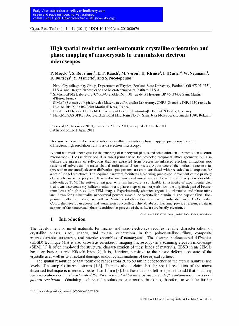
Fig. 1 Experimental set up of the ASTAR/DigiSTAR system (from NanoMEGAS) for high-resolution
crystallite orientation and phase mapping, modified after [8]. The system consists of hard- and software. The
hardware can be interfaced to any older or newer mid-voltage TEM. (No preexisting scanning facility or scanning probe
microscopy mode is required.) The bulk of the software runs on an external PC under WindowsTM. This software also
includes routines for the “straightening out” of diffraction spot patterns when the large viewing screen of the TEM is used
in its horizontal position and the patterns are recorded under some oblique angle. Courtesy of JEOL Ltd., a typical
crystallite orientation map of the distribution of copper grains in a microelectronics device structure (that was recorded at
their factory in Tokyo on a JEM-2100F field-emission microscope) and its color code are shown in the bottom-right part
of the sketch. The faint “smearing out” of the orientation contrast in the top part of this map is an unimportant artifact.
This kind of artifact can be minimized by either lowering the acquisition speed of the raw data or by using a dedicated
phosphor screen that is optimized for the high-speed recording camera. (Such a phosphor screen would need to have a
very short relaxation/“after-glow decay“ time response.) Correlation and/or reliability index thresholding during the data
processing removes this and other artifacts. (Online color at www.crt-journal.org)
Figure 1 gives an overview of the system and shows in its lower right part a typical crystallite orientation map.
Scanning PED (i.e. “off-optical-axis”) or “parallel-to-optical-axis” scanning primary electron beam (i.e. zero
precession angle) spot patterns are automatically recorded by an external digital camera (Fig. 2), while the area
of interest of the sample is scanned in a step-like fashion with a nanometer to tens of nanometer diameter
primary electron beam (as measured by its full widths at half maximum). The automated data collection step is
4 P. Moeck et al.: Orientation and phase mapping of nanocrystals
© 2011 WILEY-VCH Verlag GmbH & Co. KGaA, Weinheim www.crt-journal.org
currently followed by off-line (and prospectively also by on-line automatic) data processing. While figure 2a-c
show the new crystallite orientation and phase mapping system interfaced to two modern analytical high-
resolution TEMs, Figure 2d shows a close up view of the external CCD camera facing a TEM’s standard
fluorescent viewing screen. (Note that this optical CCD camera allows for the recording of more than 180
frames per second.)
The orientation and phase determination is performed by the matching of each experimental diffraction
pattern to a large number of templates, which are computer calculated diffraction spot patterns for all possible
orientations within the symmetry-invariant section of the stereographic projection of the corresponding crystal
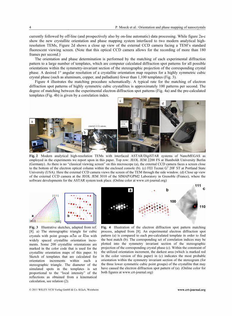
phase. A desired 1° angular resolution of a crystallite orientation map requires for a highly symmetric cubic
crystal phase (such as aluminum, copper, and palladium) fewer than 1,100 templates (Fig. 3).
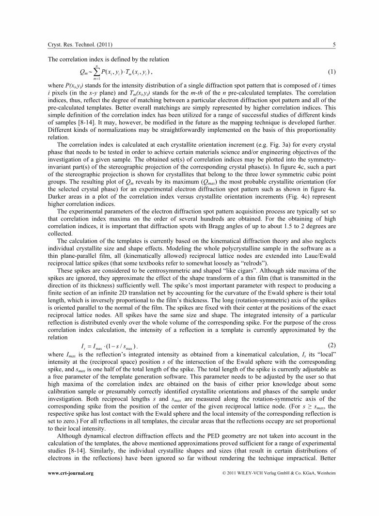
Figure 4 illustrates the matching procedure schematically. A typical rate for the matching of electron
diffraction spot patterns of highly symmetric cubic crystallites is approximately 100 patterns per second. The
degree of matching between the experimental electron diffraction spot patterns (Fig. 4a) and the pre-calculated
templates (Fig. 4b) is given by a correlation index.
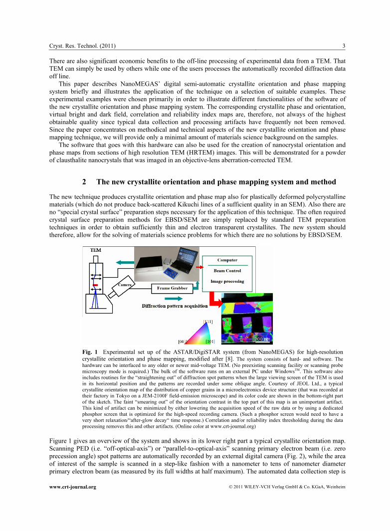
Fig. 2 Modern analytical high-resolution TEMs with interfaced ASTAR/DigiSTAR systems of NanoMEGAS as
employed in the experiments we report upon in this paper. Top row: JEOL JEM 2200 FS at Humboldt University Berlin
(Germany). As there is no “classical viewing screen” on this microscope (a), the external CCD camera faces a screen close
to the bottom of the electron optical column within the enclosed console (b). (c) FEI Tecnai G2 20F ST at Portland State
University (USA). Here the external CCD camera views the screen of the TEM through the side window. (d) Close up view
of the external CCD camera at the JEOL JEM 3010 of the SIMAP/GPM2 Laboratory in Grenoble (France), where the
software developments for the ASTAR system took place. (Online color at www.crt-journal.org)
Fig. 3 Illustrative sketches, adapted from ref.
[8]. a) The stereographic triangle for cubic
crystals with point groups m3m or 43m with
widely spaced crystallite orientation incre-
ments. Some 200 crystallite orientations are
marked in the color code that is used for the
crystallite orientation maps of this paper. b)
Sketch of templates that are calculated for
orientation increments within such a
stereographic triangle. The diameter of the
simulated spots in the templates is set
proportional to the “local intensity” of the
reflections as obtained from a kinematical
calculation, see relation (2).
Fig. 4 Illustration of the electron diffraction spot pattern matching
process, adapted from [8]. An experimental electron diffraction spot
pattern (a) is compared to each pre-calculated template in order to find
the best match (b). The corresponding set of correlation indices may be
plotted into the symmetry invariant section of the stereographic
projection of the corresponding crystal phase (c). Within the constraint of
the utilized orientation increment, the darkest area (which is marked red
in the color version of this paper) in (c) indicates the most probable
orientation within the symmetry invariant section of the stereogram (for
the three lower symmetric cubic point groups) of the crystallite that may
have caused the electron diffraction spot pattern of (a). (Online color for
both figures at www.crt-journal.org)
Cryst. Res. Technol. (2011) 5
www.crt-journal.org © 2011 WILEY-VCH Verlag GmbH & Co. KGaA, Weinheim
The correlation index is defined by the relation
Qm ∼
1
( , ) ( , )n
i i m i i
m
P x y T x y=
⋅∑ , (1)
where P(xi,yi) stands for the intensity distribution of a single diffraction spot pattern that is composed of i times
i pixels (in the x-y plane) and Tm(xi,yi) stands for the m-th of the n pre-calculated templates. The correlation
indices, thus, reflect the degree of matching between a particular electron diffraction spot pattern and all of the
pre-calculated templates. Better overall matchings are simply represented by higher correlation indices. This
simple definition of the correlation index has been utilized for a range of successful studies of different kinds
of samples [8-14]. It may, however, be modified in the future as the mapping technique is developed further.
Different kinds of normalizations may be straightforwardly implemented on the basis of this proportionality
relation.
The correlation index is calculated at each crystallite orientation increment (e.g. Fig. 3a) for every crystal
phase that needs to be tested in order to achieve certain materials science and/or engineering objectives of the
investigation of a given sample. The obtained set(s) of correlation indices may be plotted into the symmetry-
invariant part(s) of the stereographic projection of the corresponding crystal phase(s). In figure 4c, such a part
of the stereographic projection is shown for crystallites that belong to the three lower symmetric cubic point
groups. The resulting plot of Qm reveals by its maximum (Qmax) the most probable crystallite orientation (for
the selected crystal phase) for an experimental electron diffraction spot pattern such as shown in figure 4a.
Darker areas in a plot of the correlation index versus crystallite orientation increments (Fig. 4c) represent
higher correlation indices.
The experimental parameters of the electron diffraction spot pattern acquisition process are typically set so
that correlation index maxima on the order of several hundreds are obtained. For the obtaining of high
correlation indices, it is important that diffraction spots with Bragg angles of up to about 1.5 to 2 degrees are
collected.
The calculation of the templates is currently based on the kinematical diffraction theory and also neglects
individual crystallite size and shape effects. Modeling the whole polycrystalline sample in the software as a
thin plane-parallel film, all (kinematically allowed) reciprocal lattice nodes are extended into Laue/Ewald
reciprocal lattice spikes (that some textbooks refer to somewhat loosely as “relrods”).
These spikes are considered to be centrosymmetric and shaped “like cigars”. Although side maxima of the
spikes are ignored, they approximate the effect of the shape transform of a thin film (that is transmitted in the
direction of its thickness) sufficiently well. The spike’s most important parameter with respect to producing a
finite section of an infinite 2D translation net by accounting for the curvature of the Ewald sphere is their total
length, which is inversely proportional to the film’s thickness. The long (rotation-symmetric) axis of the spikes
is oriented parallel to the normal of the film. The spikes are fixed with their center at the positions of the exact
reciprocal lattice nodes. All spikes have the same size and shape. The integrated intensity of a particular
reflection is distributed evenly over the whole volume of the corresponding spike. For the purpose of the cross
correlation index calculation, the intensity of a reflection in a template is currently approximated by the
relation
max max(1 / )
sI I s s= ⋅ − , (2)
where Imax is the reflection’s integrated intensity as obtained from a kinematical calculation, Is its “local”
intensity at the (reciprocal space) position s of the intersection of the Ewald sphere with the corresponding
spike, and smax is one half of the total length of the spike. The total length of the spike is currently adjustable as
a free parameter of the template generation software. This parameter needs to be adjusted by the user so that
high maxima of the correlation index are obtained on the basis of either prior knowledge about some
calibration sample or presumably correctly identified crystallite orientations and phases of the sample under
investigation. Both reciprocal lengths s and smax are measured along the rotation-symmetric axis of the
corresponding spike from the position of the center of the given reciprocal lattice node. (For s ≥ smax, the
respective spike has lost contact with the Ewald sphere and the local intensity of the corresponding reflection is
set to zero.) For all reflections in all templates, the circular areas that the reflections occupy are set proportional
to their local intensity.
Although dynamical electron diffraction effects and the PED geometry are not taken into account in the
calculation of the templates, the above mentioned approximations proved sufficient for a range of experimental
studies [8-14]. Similarly, the individual crystallite shapes and sizes (that result in certain distributions of
electrons in the reflections) have been ignored so far without rendering the technique impractical. Better
6 P. Moeck et al.: Orientation and phase mapping of nanocrystals
© 2011 WILEY-VCH Verlag GmbH & Co. KGaA, Weinheim www.crt-journal.org
approximations for the calculation of the reflection intensities in the templates may, however, be utilized as the
technique is developed further. The Lorentz factor of the PED geometry [20] tends to enhance the intensity of
reflections in the vicinity of the primary electron beam and may also be taken into account in the future.
Since the geometry of the reflections in the templates is to a good approximation equivalent to the geometry
of experimental electron diffraction spot patterns, the success of the cross-correlation indexing procedure relies
primarily on the identification of the correct projected reciprocal lattice geometry. As the intensities of the
reflections in the templates may match to some lesser degree also the intensities in experimental electron
diffraction spot patterns, the success of the cross-correlation identification may also rely somewhat on the
reflections’ intensities.
The success of the new technique on a variety of samples [8-14] demonstrates that reasonably accurate
crystallite orientation and phase mappings are possible under highly idealized assumptions that concern the
underlying electron diffraction processes. These assumptions do, however, require not much more prior
knowledge about a sample than what is readily available in comprehensive crystallographic databases. Such
databases will, therefore, be briefly mentioned in the final section of this paper. An (crystallite orientation)
reliability index is calculated for each Qmax by the relation
2 _ _ max100 (1 / )nd highest peakR Q Q= ⋅ − , (3)
so that high reliabilities are obtained for “rather flat” Qm plots. Such a flat Qm plot is shown in figure 4c. Since
this plot has no strong second highest peak, the possibility of a mis-identification of the crystallite’s orientation
and/or phase from its electron diffraction spot pattern P(xi,yi) (Fig. 4a) is very low. Note that reliability indices
in the two digit range signify high reliabilities per definition. A reliability index in the lower one digit range, on
the other hand, indicates an ambiguous indexing. For the mapping of two crystallite phases, a “phase reliability
index”
max_ 2 _ max_1 _100 (1 / )phase nd phase st phaseR Q Q= ⋅ − (4)
needs to be utilized. When there are more than two phases to be considered, a modified phase reliability index
is used. Whenever the primary electron beam transmits two crystallites at once, e.g. adjacent grains that are
separated by a grain or phase boundary, all of the corresponding reliability indices will be low. Maps of these
indices will, therefore, ideally possess the useful feature that grain and phase boundaries will be outlined by
(what is in an image processing context know as) “tonal undershoot (dark halos)” around the corresponding
crystallites.
To produce typical crystallite orientation (see, e.g., the bottom-right part of figure 1) and phase maps,
50,000 to 250,000 experimental diffraction spot patterns are collected with an external digital camera that is
placed outside of the microscope in front of the TEM viewing screen (Figs. 1 and 2c). The diffraction spot
patterns are then stored in a dedicated file format. The acquisition frequency is synchronized with the primary
electron beam scanning and precession movements at typically 100 Hz so that less than 15 minutes to half an
hour is sufficient to acquire the required structural information from the sample for the subsequent mapping
procedures. The primary electron beam scanning and precessing movements are both controlled by the
dedicated precession hardware (add-on to the TEM) that is connected to the microscope’s sets of deflecting
coils and controlled by a dedicated remote computer. Since the scanning movement of the primary electron
beam is entirely controlled by this hard/software add-on, the microscopy itself does not need to possess a
scanning facility or a scanning probe mode†.
The data analysis, as currently performed off-line, consists of compensating for all kinds of distortions of
the experimental electron diffraction spot patterns, detecting of the location of the transmitted electron beam,
and identifying of crystallite orientations and phases through the template matching procedure as described
above. The distortions are assessed on the basis of known reference electron diffraction spot patterns for
certain sets of experimental conditions and are caused by various influences such as systematic distortion
effects of the projector lens, the inclination of the external optical camera with respect to the viewing screen,
and the uncertainty in the knowledge of the exact camera length of the TEM.
For highly symmetric small unit cell crystals, e.g. face- and body centered cubic (FCC and BCC) metals,
100 to 200 patterns may be analyzed per second. The spatial resolution limit of the mapping technique depends
on both the obtainable minimal spot size of the primary electron beam in the microscope and the freely
adjustable scanning step size. The minimal spot size depends on both the type of the electron gun used and the ____________________
† If a scanning probe facility or mode does exist on the TEM to be interfaced to a second generation (fully digital) ASTAR/DigiSTAR system or a first
generation (semi-analog) ASTAR/Spinning Star system, it will not be utilized during the recording of the experimental data and also does not interfere with
this process.

Cryst. Res. Technol. (2011) 7
www.crt-journal.org © 2011 WILEY-VCH Verlag GmbH & Co. KGaA, Weinheim
size of the aperture utilized in the second (or if present third) condenser lens. In a TEM with a field emission
electron source and a sufficiently small aperture, the minimal spot size can be on the order of 1 to 10 nm.
When nearly parallel illumination conditions can be somewhat relaxed to allow for a small primary beam
convergence, e.g. for the mapping of FCC and BCC metals, the minimal spot size might even be in the sub-
nanometer range. The scanning step size, on the other hand, is adjustable down to the order of magnitude of the
smallest obtainable spot size and can also be smaller than a nanometer.
Ideally, a nearly parallel illumination setting should be used as one wants to avoid the expansion of the
diffraction spots into disk that would result from a significant convergence of the primary electron beam. The
electron transparent area of the sample may set a limit to the size of the maps that can be obtained by the
technique. Also the specifics of the materials science and/or engineering problem that one needs to address
may impose a certain size requirement on the recorded maps.
While we usually map sample areas of less than 5 µm times 5 µm into 500 by 500 pixels, we have also
collected data for maps of up to 15 µm times 15 µm. This required comparatively large step size of 50 nm for
materials science problem adequate maps of 300 by 300 pixels.
The crystallite orientation resolution of the method depends on the angular resolution increment of the pre-
calculated templates and the precession angle. Typically this resolution is one degree or a few tenths of a
degree. The precession angle needs to be chosen judiciously in order to suppress typical thin TEM film
specimen “buckling” effects that may stem for the necessity of preparing an electron transparent film. At the
same time, higher precession angles imply lower obtainable crystallite orientation resolutions.
Experience so far has shown [8-11] that precession angles of a few tenths of a degree are often sufficient to
increase the accuracy of the method significantly while also removing thin TEM film specimen buckling
artifacts. Precession angles of up to one degree (or even somewhat larger if additional reflections from higher
order Laue zones are to be utilized) may only be beneficial for the mapping of simple inorganic materials with
very small unit cell volumes.
PED of individual crystallites results in spot patterns with more reflections‡ with partially or fully
integrated intensities. If the crystallites are not too thick and the precession angle is sufficiently large, the
intensities of PED spots may also be “less dynamical” [15,16] because “few beam” conditions [21] may have
prevailed during the precession diffraction experiments. This may result in quite effective suppressions of
dynamical diffraction effects. Few beam conditions may be approximated to two beam conditions and it is well
known that the kinematical diffraction theory is a small crystallite thickness, small electron wavelength, and
small structure factor modulus approximation to the two-beam dynamical diffraction theory when the unit cell
volumes are large [9,22,23]. For sufficiently thin crystals, PED spot intensities may, therefore, be used for
advanced structural fingerprinting in the transmission electron microscope in addition to the projected
reciprocal lattice geometry and symmetry of individual crystallites [5,9,22,23]. Since the new crystallite
orientation and phase mapping technique uses currently templates that are pre-calculated on the basis of the
kinematic diffraction theory, it is well suited to work with experimental PED data from sufficiently thin
crystallites.
For the same electron wavelength, PED brings a larger section of the Ewald sphere in contact with a
crystal’s reciprocal lattice than the conventional selected area electron diffraction technique. This is
advantageous for dealing with the so called “180° ambiguity” in the indexing of electron diffracting spot
patterns. That ambiguity arises from the fact that a particular diffraction spot in the zero order Laue zone may
be indexed as either (hkl) or )( lkh [24]. While one will obtain the same zone axis indices for both sets of
indexed reciprocal lattice vectors, an ambiguity will exist as to the azimuthal orientation of the crystal around
the zone axis. Two azimuthal orientations that differ by 180° will be equally likely. For non-centrosymmetric
cubic crystals, one may reformulate this ambiguity as being one between indexing non-symmetry equivalent
zone axes as either [uvw] or ][ wvu .
Although the 180° ambiguity is irrelevant for many applications, it becomes important for the unambiguous
determination of grain and phase boundary parameters. Methods to tackle this ambiguity are discussed in ref.
[25]. We will discuss the origin and details of this ambiguity elsewhere and also give more information there
on how we deal with it at present. Here we just mention that we have experimental evidence for the fact that
the cross correlation indexing of reflections from higher order Laue zones, as present in many precession-
enhanced electron diffraction spot patterns, is one feasible way of dealing with the 180° ambiguity. ____________________
‡ More reflections are observed experimentally in the PED mode even when the morphologies of the crystallites are highly anisotropic such as in the case of
nano-wires.

8 P. Moeck et al.: Orientation and phase mapping of nanocrystals
© 2011 WILEY-VCH Verlag GmbH & Co. KGaA, Weinheim www.crt-journal.org
With purpose written software, the second (digital) generation precession device (DigiSTAR) of NanoMEGAS
could possibly be run in a manner that emulates either the “double-rocking” technique [19] or alternative
“tilted but nearly-parallel illumination” schemes that avoid some of the shortcomings of classical precession
electron diffraction, e.g. the unavoidable simultaneous excitement of systematic rows and the need to go twice
through the Bragg condition during one precession cycle for each reflection. If the templates in the cross-
correlation procedure were to take the Lorentz factors of such tilted but nearly-parallel illumination techniques
into account, high cross correlation and reliability indices may result.
This brief introduction to the semi-automatic crystallite phase and orientation mapping technique is
complemented below by a presentation of some recent experimental results. The data for the corresponding
studies were recorded at three different microscopes, each of which equipped with PED instrumentation by
NanoMEGAS, see figures 2a,b and 2c for two of these TEMs. We show below results of our mappings of
undeformed (Figs. 5 and 6) and tensile stress deformed aluminum (Fig. 7), fine-grained palladium (Fig. 8),
polycrystalline copper (Figs. 9 and 10), and MnAs crystallites in a GaAs wafer (Figs. 11 to 13).
Fig. 5 Crystallite orientation and phase mapping of aluminum before a tensile stress deformation experiment
on the basis of ordinary (i.e. zero precession angle) electron diffraction spot patterns: (a) crystallite orientation
map, (b) correlation index map, (c) reliability index map from the same specimen area, and (d) a diffraction pattern form
the area where the scale bar is located in (a). The color code in the crystallite orientation map is the same as given (for the
crystallite orientation map of another sample) in figure 1. The arrow in (a) is discussed in the text. (Online color at
www.crt-journal.org)
Fig. 6 Crystallite orientation mapping of aluminum before a tensile stress deformation experiment on the
basis of precession-enhanced electron diffraction spot patterns (0.9° precession angle): (a) crystallite orientation
map, (b) correlation index map, (c) reliability index map from the same specimen area (as in figure 5), and (d) a diffraction
pattern from the area where the scale bar is located in (a). The color code in the crystallite orientation map is the same as in
figure 1. The arrow in (a) is discussed in the text. The higher the intensity (i.e. brightness) in (b) and (c), the higher the
numerical value of the corresponding indices. (Online color at www.crt-journal.org)
3 Experimental examples
The data for the crystallite orientation maps in figures 5 to 7b,c were collected at the Free University of
Brussels with a Philips CM20 TEM that was operated at 200 kV. This microscope features a LaB6 electron gun
and an interfaced PED device ASTAR/DigiSTAR from NanoMEGAS. Polycrystalline aluminum before (Figs.
5 and 6) and after (Fig. 7) tensile stress deformation experiments served as samples.
In order to demonstrate the effect of the PED mode on the accuracy of the technique, the analysis was
performed twice for the same ensemble of nanocrystals (Figs. 5 and 6). While the data of figure 5 were
recorded with a non-precessing primary electron beam, their counterpart data in figure 6 were recorded with a
precession angle of 0.9°. The step size was in each case 10 nm. The diameter of the primary electron beam was
Cryst. Res. Technol. (2011) 9
www.crt-journal.org © 2011 WILEY-VCH Verlag GmbH & Co. KGaA, Weinheim
approximately 8 nm. There has been no correlation index thresholding in both crystallite orientation maps
(Figs. 5a and 6a) and in the corresponding reliability index maps (Figs. 5c and 6c). This processing step has
been omitted on purpose in order to clarify its importance in removing artifacts. The “essentially black” areas
(around the figure labels in the bottom-right corners) of the correlation index maps (Figs. 5b and 6b) possess a
correlation index of essentially zero. This means that these areas represent the edge of the sample to the
vacuum within the microscope. There is again a faint and rather unimportant “smearing out” artifact in both of
these maps for the reasons discussed in the caption of figure 1. However, enforcing a suitable correlation index
threshold on the crystallite orientation and reliability maps (Figs. 5a, 6a, 5c, and 6c) would, reveal the sample
edge to the vacuum (in the bottom-right corners of these maps) as well.
Comparing the first three panels of figures 5 and 6 with each other, one can see that the crystallite
orientation map which is based on PED data is much “clearer”, that the corresponding correlation index map is
“much brighter”, and that the corresponding reliability index map is both “brighter and clearer”. “Clearness” in
the crystallite orientation and reliability index maps corresponds to pixel value homogeneity throughout some
neighboring areas. Higher brightness in both the correlation index and reliability index maps means simply that
the numerical values of the indices are higher on average.
In the sense discussed in the introduction of this paper, it is clear that the crystallite orientation map on the
basis of PED data represents “more accurately” the true orientation distribution in the sample. Note that some
crystallites show a rather significantly different color in the crystallite orientation maps of figures 5a and 6a.
One such crystallite with an orientation difference between the two crystallite orientation maps of roughly 20°
is marked in both maps by the tip of an arrow. One may, thus, say that a part of the crystallite orientation map
for the zero precession angle (Fig. 5a) is in error. The PED-data based reliability index map of Fig. 6c shows
that precession results in a significant increase of the reliability index throughout the area of this particular
crystallite so that the “interior” of the crystallite and the surrounding grain boundaries are both clearly
revealed. This is not the case for this particular crystallite in the reliability index map for zero precession angle
(Fig. 5c) so that the advantage of the PED mode for crystallite orientation mapping has been clearly illustrated.
Simulations by other authors for zero precession angle data have shown that the immediate orientation
environment of certain low indexed zone axis patterns, e.g. [112] and [013] in FCC metals (such as aluminum),
are particularly difficult to index by cross-correlation techniques, see ref. [26] for more details. While [112]
roughly corresponds to the color of the crystallite that is marked by the tip of the arrow in figure 6a, [013]
corresponds roughly to a bright shade of the color yellow. At some later stage of the development of the cross
correlation software, such predictable difficulties in obtaining high correlation indices for certain crystallite
orientations of certain structures may be corrected by some kind of a “structure dependent” normalization.
For now it is probably more than sheer coincidence that the application of the PED mode reveals an
approximately [112] oriented grain in a crystallite orientation map of a FCC metal clearly, see tip of the arrow
in figure 6a, while it seems to have been mis-indexed on the basis on data that were recorded with a (scanning)
parallel-to-optical-axis primary beam, see corresponding area in figure 5a. Also the color of the very small
crystallite underneath the “m” of the “μm” annotation in figure 5a changed from bright yellow for the scanning
parallel-to-optical-axis primary beam data to light blue in figure 6a for the PED data. The corresponding area
also appears rather dark in the reliability index map (Fig. 5c) in agreement with the above mentioned
simulations [26], while it is rather bright in the counterpart map that is based on PED data (Fig. 6c).
The comparison of the two electron diffraction spot patterns in the last panel of figures 5 and 6 from the
crystallite underneath the scale bar in figures 5a and 6a (where the arrows start) illustrates not only the main
advantage of the PED mode, i.e. more reflections, but also reveals evidence for the suppression of multiple
electron diffraction effects. Such effects resulted for this particular crystallite in the formation of Kikuchi lines
in the zero precession angle pattern of figure 5d.
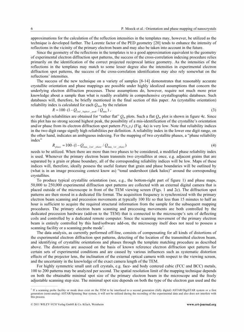
Figure 7a shows the negative of a conventional bright field TEM image of a tensile stressed aluminum
sample. The data for the crystallite orientation mapping of this sample were recorded with a precession angle
of 0.9° (Fig. 7b). The step size for the recording of this map was 10 nm. The diameter of the primary electron
beam was approximately 8 nm. Note that a larger sample area than visible on the conventional TEM negative
was scanned-precessed for this purpose. Also shown is the superposition of this crystallite orientation map with
the corresponding reliability index map (Fig. 7c). Some of the grains that are oriented close to [112] possess
again a low reliability index as marked by arrows in figure 7c. Other grains close to this orientation do,
however, possess low reliability indices only at their clearly visibly grain boundaries, i.e. do not appear dark in
their interiors in figure 7c. It might, therefore, be the case that some of the “dark grains” in figure 7c are due to
superpositions of more than one grain in the direction of the transmitted electron beam. The hole in the sample
10 P. Moeck et al.: Orientation and phase mapping of nanocrystals
© 2011 WILEY-VCH Verlag GmbH & Co. KGaA, Weinheim www.crt-journal.org
appears in a green color in figure 7b due to the above (in the caption of figure 1) mentioned slight smearing out
effect of a fast data acquisition process. Figure 7c clarifies that the orientation reliability within that particular
sample area is very low. That area may be removed from the crystallite orientation map by a suitable reliability
index thresholding.
Fig. 7 Crystallite orientation mapping of
polycrystalline aluminum after tensile stressing
(0.9° precession angle): (a) TEM bright field
image as recorded on photographic film, (b)
crystallite orientation map, (c) crystallite orientation
map overlaid with the corresponding reliability index
map (from the same specimen). Note both the
“necking” and hole in (a) that resulted from the
tensile stressing. The location of this hole is
indicated with a dotted circle in all three panels. As
one would expect, the reliability of “indexing” the
area of the hole is very low, i.e. this area appears
dark in (c). For illustrative purposes, the area of the
vacuum in the microscope has been set to appear red
in (b) and (c). (Online color at www.crt-journal.org)
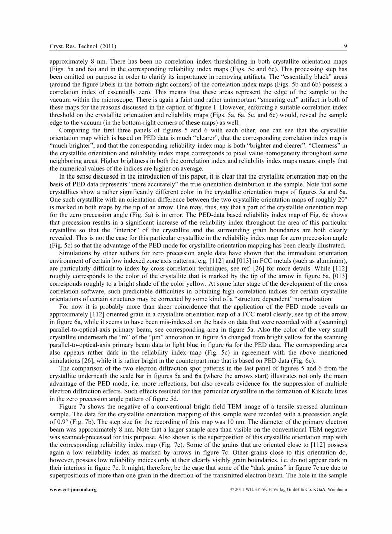
At the JEOL JEM 2200FS of Humboldt University Berlin that possesses both a field-emission gun and an in-
column Ω energy filter, the data for the maps of figure 8 were collected at 200 kV within three minutes from a
fine-grained palladium sample. A PED device ASTAR/DigiSTAR from NanoMEGAS is interfaced to this
microscope and it serves as demo site for this company for middle Europe. While the scanning-precessing step
size of the primary electron beam was for these experiments set to 0.4 nm, the full widths at half maximum of
the primary electron beam was approximately 0.5 nm. Such a small-size nearly parallel primary electron beam
is possible in this microscope due to its field emission source and a 10 μm diameter aperture in the condenser.
For the applied mapping technique, one may infer a maximal spatial resolution of approximately 1 nm from
the “crystallite mis-orientation versus line scan direction” plot in figure 8d. This inference is based of the very
faint visibility of a “partially enclosed” crystallite (of roughly that width) within a clearly visible (about 6 nm
wide) crystallite that appears blue in the crystallite orientation map (Fig. 8a) and is marked there by a thin
straight bar.
Fig. 8 Crystallite orientation mapping of fine-grained palladium (0.9° precession angle): (a) crystallite
orientation map, (b) crystallite orientation map overlaid with the corresponding reliability index map, (c) correlation index
map from the same specimen area. Note that the thin bars in all three maps that cross two crystallites are 8 nm long and
represent the x-axis in the crystallite mis-orientation versus line scan direction plot in (d). This 8 nm bar is most clearly
visible in (b) and divided into 20 sections of 0.4 nm each (that represent the utilized scanning-precession increments of the
primary electron beam) in (d). The color code in the crystallite orientation map is the same as in figures 1 and 7b. (Online
color at www.crt-journal.org)
The same crystallites/bar combination is also visible in both figure 8b and the correlation index map figure 8c.
The visibility of the partially enclosed crystallite is best in the crystallite orientation map overlaid with the
reliability index map in the second panel of figure 8, where it appears dark and the superimposed bar appears
bright. This “very narrow” crystallite could possibly be a 111 twin because the observed “almost 60° jumps”
in the crystallite mis-orientation versus line scan direction plot in figure 8d can be thought to arise from the
cross-correlation indexing of 180° twins for cubic materials with point group m3m. Note that figure 8d reveals
almost 60° jumps in the local mis-orientation profile along the 8 nm wide bar between sections 3 and 4, 9 and
10, as well as 11 and 12. This crystallite is, thus, sampled by the scanning-precessing primary electron beam at
only two spatial positions which are 0.4 nm apart. For a much clearer representation of a crystallite in a

Cryst. Res. Technol. (2011) 11
www.crt-journal.org © 2011 WILEY-VCH Verlag GmbH & Co. KGaA, Weinheim
crystallite orientation map, one would probably need a sampling at twice or thrice as many scanning-precession
increments. A maximal spatial resolution of 1 nm, thus, may correspond to a “more readily discernable” spatial
resolution of 2 to 3 nm.
Two crystallites in twin orientation in a FCC metal share a 111 plane and are mis-oriented with respect to
each other by a rotation of 180° around the normal of the twin plane. This normal is a <111> zone axis with
point symmetry 3m. Symmetry equivalent directions within a 111 plane possess, therefore, a multiplicity of
6, with mis-orientations of 60° (and multiples of 60°) around the corresponding zone axis directions.
One may, for example, consider a specific twin plane in a FCC metal, e.g. (111), viewed edge on. If one
crystallite is oriented with its [112] direction parallel to the optical axis of the TEM, its twin will be oriented
with its [112] direction with respect to this axis. The orientations [121], [211], [121], and [211] are all
symmetry equivalent to these two orientations and also lie in the (111) plane so that the cross correlation
software cannot distinguish between them.
If the (111) twin plane is not viewed edge on, the multiplicity of crystallite orientations with respect to the
twin plane is 12. This would results in “four sets” of symmetry equivalent crystallite orientations which are
mis-oriented with respect to each other by 120° (and multiples of 120°) around the [111] zone axis.
When theses basic crystallographic facts are combined with the 180° indexing ambiguity, mis-orientations
of 60° (i.e. the difference between 180° and 120°) are likely to be observed for inclined (111) twin planes as
well. In conclusions, mis-orientations of approximately 60° between two FCC crystallites that share a more or
less straight grain boundary are often associated with twinning, but there can certainly be other grain
boundaries with this characteristic that are not twin boundaries.
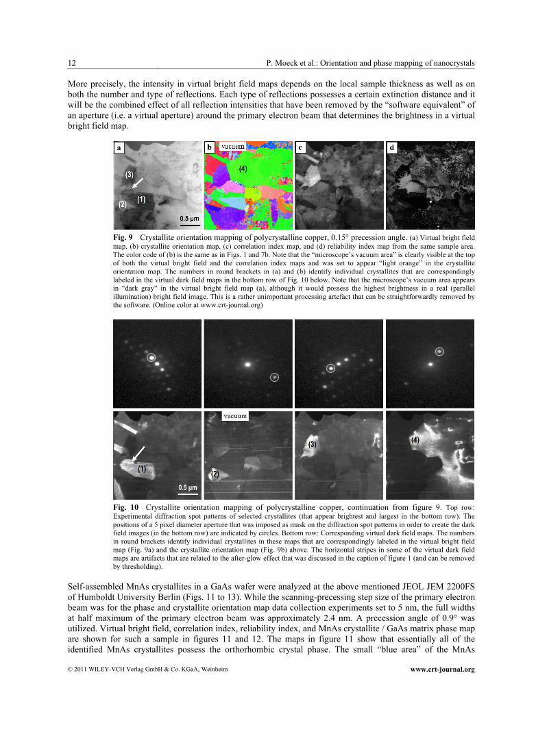
Thin polycrystalline copper films were analyzed at the FEI Tecnai G2 F20 ST analytical field-emission
microscope of Portland State University. This microscope is also equipped with an ASTAR/DigiSTAR system
of NanoMEGAS and serves as demonstration site for this company for the USA. Due to its field emission
source, nanometer sized primary electron beams with small convergence angles can be utilized in this
microscope (with a 10 μm diameter aperture in the second condenser lens) in conjunction with suitably small
step sizes.
While the step size was set to 150 nm in the analyses of the polycrystalline copper films in order to cover
wide sample areas, a primary electron beam with a diameter of approximately 20 nm was used. A low
precession angle of 0.15° was used for the analyses, although the unit cell volume of copper is smaller than that
of aluminum and palladium. The virtual bright field (Fig. 9a), crystallite orientation (Fig. 9b), correlation index
(Fig. 9c), reliability index (Fig. 9d), and virtual dark field maps in the bottom row of figure 10 may, therefore,
contain some thin film buckling artifacts. The crystallite orientation map (Fig. 9b) shows nevertheless
sufficient pixel value homogeneity throughout many of the crystallites.
Virtual dark field images of individual crystallites or crystallite areas are obtained with the ASTAR
software by a simple (computer) prompt after a suitable “virtual aperture” has been set around a particular
reflection spot in one of the automatically recorded electron diffraction patterns from that crystallite. The
corresponding dark field map then shows the crystallite or crystallite areas with bright contrast together with all
of the various sample areas that contribute to the diffracted intensity within the virtual aperture.
The experimental electron diffraction spot patterns that form the basis for the crystallite mapping process
can simply be displayed by clicking with the mouse on a crystallite in either the virtual bright field map or the
crystallite orientation map. In the top row of figure 10, four such electron diffraction patterns are shown.
Due to the comparatively small precession angle, resemblances of “dynamical diffraction contrast” should
be present in the virtual bright field map (Fig. 9a) and the virtual dark field maps, bottom row of figure 10.
This is indeed the case as marked by arrows in figure 9a and the virtual dark field image in the first column of
the bottom row of figure 10. While thickness fringes (of classical diffraction contrast) are a sequence of bright
and dark stripes at the edge of a crystallite in the virtual bright field image of the marked crystallite, the
contrast is reversed in the corresponding virtual dark field image. This kind of quasi-classical diffraction
contrast at low precession angles will have its usage in more thorough off-line analyses of polycrystalline
materials. Large precession angles, on the other hand, tend to average such contrasts out.
As a “rule of thumb”, crystallites that appear dark in a virtual bright field map are for sufficiently thin
samples often associated with electron diffraction spot patterns that possess many reflections. These crystallites
in turn tend to possess high correlation indices and appear, therefore, bright in a correlation index map. For an
illustration of these relationships, compare individual crystallites and their contrast in figures 9a and 9c, their
experimental electron diffraction spot patterns, and their contrast in the virtual dark field maps of figure 10.
12 P. Moeck et al.: Orientation and phase mapping of nanocrystals
© 2011 WILEY-VCH Verlag GmbH & Co. KGaA, Weinheim www.crt-journal.org
More precisely, the intensity in virtual bright field maps depends on the local sample thickness as well as on
both the number and type of reflections. Each type of reflections possesses a certain extinction distance and it
will be the combined effect of all reflection intensities that have been removed by the “software equivalent” of
an aperture (i.e. a virtual aperture) around the primary electron beam that determines the brightness in a virtual
bright field map.
Fig. 9 Crystallite orientation mapping of polycrystalline copper, 0.15° precession angle. (a) Virtual bright field
map, (b) crystallite orientation map, (c) correlation index map, and (d) reliability index map from the same sample area.
The color code of (b) is the same as in Figs. 1 and 7b. Note that the “microscope’s vacuum area” is clearly visible at the top
of both the virtual bright field and the correlation index maps and was set to appear “light orange” in the crystallite
orientation map. The numbers in round brackets in (a) and (b) identify individual crystallites that are correspondingly
labeled in the virtual dark field maps in the bottom row of Fig. 10 below. Note that the microscope’s vacuum area appears
in “dark gray” in the virtual bright field map (a), although it would possess the highest brightness in a real (parallel
illumination) bright field image. This is a rather unimportant processing artefact that can be straightforwardly removed by
the software. (Online color at www.crt-journal.org)
Fig. 10 Crystallite orientation mapping of polycrystalline copper, continuation from figure 9. Top row:
Experimental diffraction spot patterns of selected crystallites (that appear brightest and largest in the bottom row). The
positions of a 5 pixel diameter aperture that was imposed as mask on the diffraction spot patterns in order to create the dark
field images (in the bottom row) are indicated by circles. Bottom row: Corresponding virtual dark field maps. The numbers
in round brackets identify individual crystallites in these maps that are correspondingly labeled in the virtual bright field
map (Fig. 9a) and the crystallite orientation map (Fig. 9b) above. The horizontal stripes in some of the virtual dark field
maps are artifacts that are related to the after-glow effect that was discussed in the caption of figure 1 (and can be removed
by thresholding).
Self-assembled MnAs crystallites in a GaAs wafer were analyzed at the above mentioned JEOL JEM 2200FS
of Humboldt University Berlin (Figs. 11 to 13). While the scanning-precessing step size of the primary electron
beam was for the phase and crystallite orientation map data collection experiments set to 5 nm, the full widths
at half maximum of the primary electron beam was approximately 2.4 nm. A precession angle of 0.9° was
utilized. Virtual bright field, correlation index, reliability index, and MnAs crystallite / GaAs matrix phase map
are shown for such a sample in figures 11 and 12. The maps in figure 11 show that essentially all of the
identified MnAs crystallites possess the orthorhombic crystal phase. The small “blue area” of the MnAs
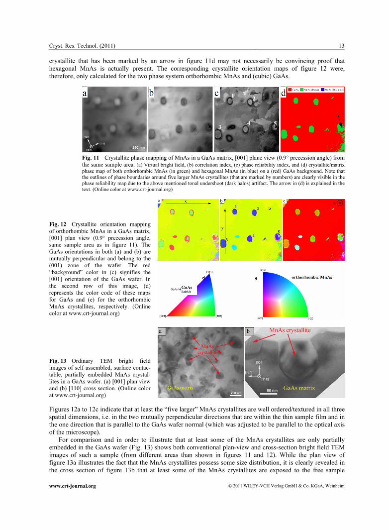
Cryst. Res. Technol. (2011) 13
www.crt-journal.org © 2011 WILEY-VCH Verlag GmbH & Co. KGaA, Weinheim
crystallite that has been marked by an arrow in figure 11d may not necessarily be convincing proof that
hexagonal MnAs is actually present. The corresponding crystallite orientation maps of figure 12 were,
therefore, only calculated for the two phase system orthorhombic MnAs and (cubic) GaAs.
Fig. 11 Crystallite phase mapping of MnAs in a GaAs matrix, [001] plane view (0.9° precession angle) from
the same sample area. (a) Virtual bright field, (b) correlation index, (c) phase reliability index, and (d) crystallite/matrix
phase map of both orthorhombic MnAs (in green) and hexagonal MnAs (in blue) on a (red) GaAs background. Note that
the outlines of phase boundaries around five larger MnAs crystallites (that are marked by numbers) are clearly visible in the
phase reliability map due to the above mentioned tonal undershoot (dark halos) artifact. The arrow in (d) is explained in the
text. (Online color at www.crt-journal.org)
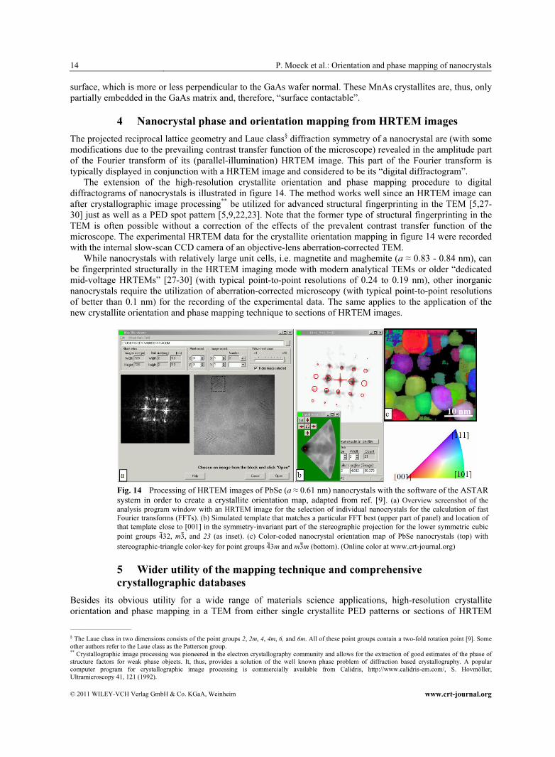
Fig. 12 Crystallite orientation mapping
of orthorhombic MnAs in a GaAs matrix,
[001] plan view (0.9° precession angle,
same sample area as in figure 11). The
GaAs orientations in both (a) and (b) are
mutually perpendicular and belong to the
(001) zone of the wafer. The red
“background” color in (c) signifies the
[001] orientation of the GaAs wafer. In
the second row of this image, (d)
represents the color code of these maps
for GaAs and (e) for the orthorhombic
MnAs crystallites, respectively. (Online
color at www.crt-journal.org)
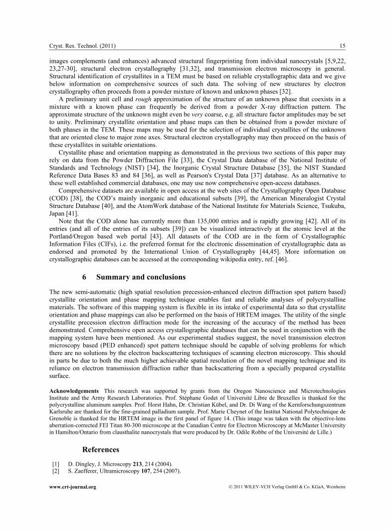
Fig. 13 Ordinary TEM bright field
images of self assembled, surface contac-
table, partially embedded MnAs crystal-
lites in a GaAs wafer. (a) [001] plan view
and (b) [110] cross section. (Online color
at www.crt-journal.org)
Figures 12a to 12c indicate that at least the “five larger” MnAs crystallites are well ordered/textured in all three
spatial dimensions, i.e. in the two mutually perpendicular directions that are within the thin sample film and in
the one direction that is parallel to the GaAs wafer normal (which was adjusted to be parallel to the optical axis
of the microscope).
For comparison and in order to illustrate that at least some of the MnAs crystallites are only partially
embedded in the GaAs wafer (Fig. 13) shows both conventional plan-view and cross-section bright field TEM
images of such a sample (from different areas than shown in figures 11 and 12). While the plan view of
figure 13a illustrates the fact that the MnAs crystallites possess some size distribution, it is clearly revealed in
the cross section of figure 13b that at least some of the MnAs crystallites are exposed to the free sample
14 P. Moeck et al.: Orientation and phase mapping of nanocrystals
© 2011 WILEY-VCH Verlag GmbH & Co. KGaA, Weinheim www.crt-journal.org
surface, which is more or less perpendicular to the GaAs wafer normal. These MnAs crystallites are, thus, only
partially embedded in the GaAs matrix and, therefore, “surface contactable”.
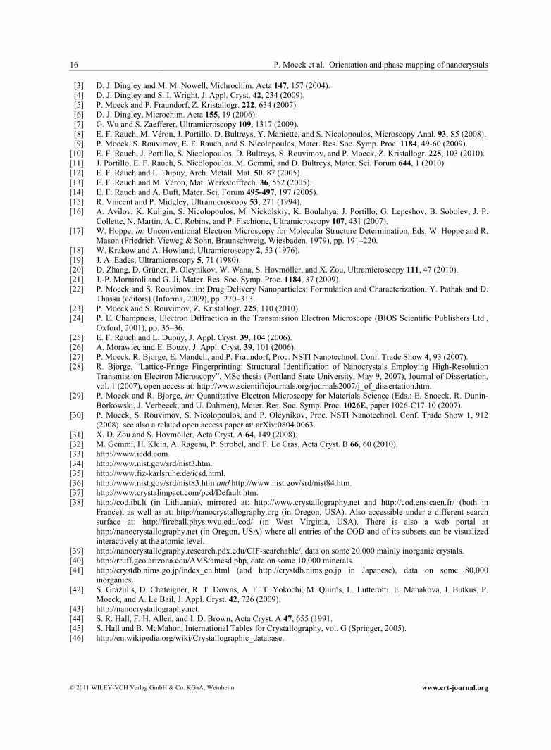
4 Nanocrystal phase and orientation mapping from HRTEM images
The projected reciprocal lattice geometry and Laue class§ diffraction symmetry of a nanocrystal are (with some
modifications due to the prevailing contrast transfer function of the microscope) revealed in the amplitude part
of the Fourier transform of its (parallel-illumination) HRTEM image. This part of the Fourier transform is
typically displayed in conjunction with a HRTEM image and considered to be its “digital diffractogram”.
The extension of the high-resolution crystallite orientation and phase mapping procedure to digital
diffractograms of nanocrystals is illustrated in figure 14. The method works well since an HRTEM image can
after crystallographic image processing** be utilized for advanced structural fingerprinting in the TEM [5,27-
30] just as well as a PED spot pattern [5,9,22,23]. Note that the former type of structural fingerprinting in the
TEM is often possible without a correction of the effects of the prevalent contrast transfer function of the
microscope. The experimental HRTEM data for the crystallite orientation mapping in figure 14 were recorded
with the internal slow-scan CCD camera of an objective-lens aberration-corrected TEM.
While nanocrystals with relatively large unit cells, i.e. magnetite and maghemite (a ≈ 0.83 - 0.84 nm), can
be fingerprinted structurally in the HRTEM imaging mode with modern analytical TEMs or older “dedicated
mid-voltage HRTEMs” [27-30] (with typical point-to-point resolutions of 0.24 to 0.19 nm), other inorganic
nanocrystals require the utilization of aberration-corrected microscopy (with typical point-to-point resolutions
of better than 0.1 nm) for the recording of the experimental data. The same applies to the application of the
new crystallite orientation and phase mapping technique to sections of HRTEM images.
Fig. 14 Processing of HRTEM images of PbSe (a ≈ 0.61 nm) nanocrystals with the software of the ASTAR
system in order to create a crystallite orientation map, adapted from ref. [9]. (a) Overview screenshot of the
analysis program window with an HRTEM image for the selection of individual nanocrystals for the calculation of fast
Fourier transforms (FFTs). (b) Simulated template that matches a particular FFT best (upper part of panel) and location of
that template close to [001] in the symmetry-invariant part of the stereographic projection for the lower symmetric cubic
point groups 432, m3, and 23 (as inset). (c) Color-coded nanocrystal orientation map of PbSe nanocrystals (top) with
stereographic-triangle color-key for point groups 43m and m3m (bottom). (Online color at www.crt-journal.org)
5 Wider utility of the mapping technique and comprehensive
crystallographic databases
Besides its obvious utility for a wide range of materials science applications, high-resolution crystallite
orientation and phase mapping in a TEM from either single crystallite PED patterns or sections of HRTEM
____________________
§ The Laue class in two dimensions consists of the point groups 2, 2m, 4, 4m, 6, and 6m. All of these point groups contain a two-fold rotation point [9]. Some
other authors refer to the Laue class as the Patterson group. ** Crystallographic image processing was pioneered in the electron crystallography community and allows for the extraction of good estimates of the phase of
structure factors for weak phase objects. It, thus, provides a solution of the well known phase problem of diffraction based crystallography. A popular
computer program for crystallographic image processing is commercially available from Calidris, http://www.calidris-em.com/, S. Hovmöller,
Ultramicroscopy 41, 121 (1992).
Cryst. Res. Technol. (2011) 15
www.crt-journal.org © 2011 WILEY-VCH Verlag GmbH & Co. KGaA, Weinheim
images complements (and enhances) advanced structural fingerprinting from individual nanocrystals [5,9,22,
23,27-30], structural electron crystallography [31,32], and transmission electron microscopy in general.
Structural identification of crystallites in a TEM must be based on reliable crystallographic data and we give
below information on comprehensive sources of such data. The solving of new structures by electron
crystallography often proceeds from a powder mixture of known and unknown phases [32].
A preliminary unit cell and rough approximation of the structure of an unknown phase that coexists in a
mixture with a known phase can frequently be derived from a powder X-ray diffraction pattern. The
approximate structure of the unknown might even be very coarse, e.g. all structure factor amplitudes may be set
to unity. Preliminary crystallite orientation and phase maps can then be obtained from a powder mixture of
both phases in the TEM. These maps may be used for the selection of individual crystallites of the unknown
that are oriented close to major zone axes. Structural electron crystallography may then proceed on the basis of
these crystallites in suitable orientations.
Crystallite phase and orientation mapping as demonstrated in the previous two sections of this paper may
rely on data from the Powder Diffraction File [33], the Crystal Data database of the National Institute of
Standards and Technology (NIST) [34], the Inorganic Crystal Structure Database [35], the NIST Standard
Reference Data Bases 83 and 84 [36], as well as Pearson's Crystal Data [37] database. As an alternative to
these well established commercial databases, one may use now comprehensive open-access databases.
Comprehensive datasets are available in open access at the web sites of the Crystallography Open Database
(COD) [38], the COD’s mainly inorganic and educational subsets [39], the American Mineralogist Crystal
Structure Database [40], and the AtomWork database of the National Institute for Materials Science, Tsukuba,
Japan [41].
Note that the COD alone has currently more than 135,000 entries and is rapidly growing [42]. All of its
entries (and all of the entries of its subsets [39]) can be visualized interactively at the atomic level at the
Portland/Oregon based web portal [43]. All datasets of the COD are in the form of Crystallographic
Information Files (CIFs), i.e. the preferred format for the electronic dissemination of crystallographic data as
endorsed and promoted by the International Union of Crystallography [44,45]. More information on
crystallographic databases can be accessed at the corresponding wikipedia entry, ref. [46].
6 Summary and conclusions
The new semi-automatic (high spatial resolution precession-enhanced electron diffraction spot pattern based)
crystallite orientation and phase mapping technique enables fast and reliable analyses of polycrystalline
materials. The software of this mapping system is flexible in its intake of experimental data so that crystallite
orientation and phase mappings can also be performed on the basis of HRTEM images. The utility of the single
crystallite precession electron diffraction mode for the increasing of the accuracy of the method has been
demonstrated. Comprehensive open access crystallographic databases that can be used in conjunction with the
mapping system have been mentioned. As our experimental studies suggest, the novel transmission electron
microscopy based (PED enhanced) spot pattern technique should be capable of solving problems for which
there are no solutions by the electron backscattering techniques of scanning electron microscopy. This should
in parts be due to both the much higher achievable spatial resolution of the novel mapping technique and its
reliance on electron transmission diffraction rather than backscattering from a specially prepared crystallite
surface.
Acknowledgements This research was supported by grants from the Oregon Nanoscience and Microtechnologies
Institute and the Army Research Laboratories. Prof. Stéphane Godet of Université Libre de Bruxelles is thanked for the
polycrystalline aluminum samples. Prof. Horst Hahn, Dr. Christian Kübel, and Dr. Di Wang of the Kernforschungszentrum
Karlsruhe are thanked for the fine-grained palladium sample. Prof. Marie Cheynet of the Institut National Polytechnique de
Grenoble is thanked for the HRTEM image in the first panel of figure 14. (This image was taken with the objective-lens
aberration-corrected FEI Titan 80-300 microscope at the Canadian Centre for Electron Microscopy at McMaster University
in Hamilton/Ontario from clausthalite nanocrystals that were produced by Dr. Odile Robbe of the Université de Lille.)
References
[1] D. Dingley, J. Microscopy 213, 214 (2004).
[2] S. Zaefferer, Ultramicroscopy 107, 254 (2007).
16 P. Moeck et al.: Orientation and phase mapping of nanocrystals
© 2011 WILEY-VCH Verlag GmbH & Co. KGaA, Weinheim www.crt-journal.org
[3] D. J. Dingley and M. M. Nowell, Michrochim. Acta 147, 157 (2004).
[4] D. J. Dingley and S. I. Wright, J. Appl. Cryst. 42, 234 (2009).
[5] P. Moeck and P. Fraundorf, Z. Kristallogr. 222, 634 (2007).
[6] D. J. Dingley, Microchim. Acta 155, 19 (2006).
[7] G. Wu and S. Zaefferer, Ultramicroscopy 109, 1317 (2009).
[8] E. F. Rauch, M. Véron, J. Portillo, D. Bultreys, Y. Maniette, and S. Nicolopoulos, Microscopy Anal. 93, S5 (2008).
[9] P. Moeck, S. Rouvimov, E. F. Rauch, and S. Nicolopoulos, Mater. Res. Soc. Symp. Proc. 1184, 49-60 (2009).
[10] E. F. Rauch, J. Portillo, S. Nicolopoulos, D. Bultreys, S. Rouvimov, and P. Moeck, Z. Kristallogr. 225, 103 (2010).
[11] J. Portillo, E. F. Rauch, S. Nicolopoulos, M. Gemmi, and D. Bultreys, Mater. Sci. Forum 644, 1 (2010).
[12] E. F. Rauch and L. Dupuy, Arch. Metall. Mat. 50, 87 (2005).
[13] E. F. Rauch and M. Véron, Mat. Werkstofftech. 36, 552 (2005).
[14] E. F. Rauch and A. Duft, Mater. Sci. Forum 495-497, 197 (2005).
[15] R. Vincent and P. Midgley, Ultramicroscopy 53, 271 (1994).
[16] A. Avilov, K. Kuligin, S. Nicolopoulos, M. Nickolskiy, K. Boulahya, J. Portillo, G. Lepeshov, B. Sobolev, J. P.
Collette, N. Martin, A. C. Robins, and P. Fischione, Ultramicroscopy 107, 431 (2007).
[17] W. Hoppe, in: Unconventional Electron Microscopy for Molecular Structure Determination, Eds. W. Hoppe and R.
Mason (Friedrich Vieweg & Sohn, Braunschweig, Wiesbaden, 1979), pp. 191–220.
[18] W. Krakow and A. Howland, Ultramicroscopy 2, 53 (1976).
[19] J. A. Eades, Ultramicroscopy 5, 71 (1980).
[20] D. Zhang, D. Grüner, P. Oleynikov, W. Wana, S. Hovmöller, and X. Zou, Ultramicroscopy 111, 47 (2010).
[21] J.-P. Morniroli and G. Ji, Mater. Res. Soc. Symp. Proc. 1184, 37 (2009).
[22] P. Moeck and S. Rouvimov, in: Drug Delivery Nanoparticles: Formulation and Characterization, Y. Pathak and D.
Thassu (editors) (Informa, 2009), pp. 270–313.
[23] P. Moeck and S. Rouvimov, Z. Kristallogr. 225, 110 (2010).
[24] P. E. Champness, Electron Diffraction in the Transmission Electron Microscope (BIOS Scientific Publishers Ltd.,
Oxford, 2001), pp. 35–36.
[25] E. F. Rauch and L. Dupuy, J. Appl. Cryst. 39, 104 (2006).
[26] A. Morawiec and E. Bouzy, J. Appl. Cryst. 39, 101 (2006).
[27] P. Moeck, R. Bjorge, E. Mandell, and P. Fraundorf, Proc. NSTI Nanotechnol. Conf. Trade Show 4, 93 (2007).
[28] R. Bjorge, “Lattice-Fringe Fingerprinting: Structural Identification of Nanocrystals Employing High-Resolution
Transmission Electron Microscopy”, MSc thesis (Portland State University, May 9, 2007), Journal of Dissertation,
vol. 1 (2007), open access at: http://www.scientificjournals.org/journals2007/j_of_dissertation.htm.
[29] P. Moeck and R. Bjorge, in: Quantitative Electron Microscopy for Materials Science (Eds.: E. Snoeck, R. Dunin-
Borkowski, J. Verbeeck, and U. Dahmen), Mater. Res. Soc. Symp. Proc. 1026E, paper 1026-C17-10 (2007).
[30] P. Moeck, S. Rouvimov, S. Nicolopoulos, and P. Oleynikov, Proc. NSTI Nanotechnol. Conf. Trade Show 1, 912
(2008). see also a related open access paper at: arXiv:0804.0063.
[31] X. D. Zou and S. Hovmöller, Acta Cryst. A 64, 149 (2008).
[32] M. Gemmi, H. Klein, A. Rageau, P. Strobel, and F. Le Cras, Acta Cryst. B 66, 60 (2010).
[33] http://www.icdd.com.
[34] http://www.nist.gov/srd/nist3.htm.
[35] http://www.fiz-karlsruhe.de/icsd.html.
[36] http://www.nist.gov/srd/nist83.htm and http://www.nist.gov/srd/nist84.htm.
[37] http://www.crystalimpact.com/pcd/Default.htm.
[38] http://cod.ibt.lt (in Lithuania), mirrored at: http://www.crystallography.net and http://cod.ensicaen.fr/ (both in
France), as well as at: http://nanocrystallography.org (in Oregon, USA). Also accessible under a different search
surface at: http://fireball.phys.wvu.edu/cod/ (in West Virginia, USA). There is also a web portal at
http://nanocrystallography.net (in Oregon, USA) where all entries of the COD and of its subsets can be visualized
interactively at the atomic level.
[39] http://nanocrystallography.research.pdx.edu/CIF-searchable/, data on some 20,000 mainly inorganic crystals.
[40] http://rruff.geo.arizona.edu/AMS/amcsd.php, data on some 10,000 minerals.
[41] http://crystdb.nims.go.jp/index_en.html (and http://crystdb.nims.go.jp in Japanese), data on some 80,000
inorganics.
[42] S. Gražulis, D. Chateigner, R. T. Downs, A. F. T. Yokochi, M. Quirós, L. Lutterotti, E. Manakova, J. Butkus, P.
Moeck, and A. Le Bail, J. Appl. Cryst. 42, 726 (2009).
[43] http://nanocrystallography.net.
[44] S. R. Hall, F. H. Allen, and I. D. Brown, Acta Cryst. A 47, 655 (1991.
[45] S. Hall and B. McMahon, International Tables for Crystallography, vol. G (Springer, 2005).
[46] http://en.wikipedia.org/wiki/Crystallographic_database.